Embed Size (px)
Citation preview
Activity reports Kobe Univ. /ICEPP Tokyo
-- MicroMEGAS with sputtering anodes --
Atsuhiko OchiKobe University
25/06/2013 New Small Wheel MicroMegas Mechanics and layout Workshop
About sputtering micromegas First operation test for sputtering
micromegas. The mechanical structure ideas for large
size production Future plan
25/04/2013A. Ochi, MMM workshop 2
Outline
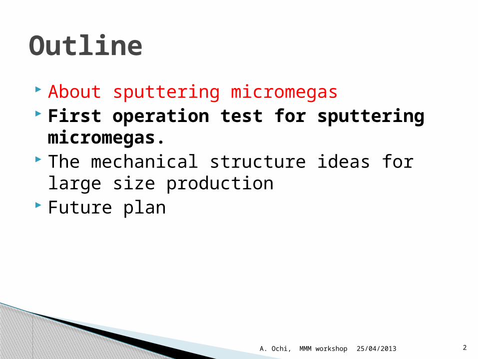
Screen printing is used for current prototypes (@ CERN and Japan)◦ 400 μm pitch was available, but less
pitch is very difficult (in our experience)
We have proposed new technique :Sputtering with lift off process◦ Less than half pitch of readout strips
can be formed We will not need to take care the
alignment between resistive strips and readouts.(We have to confirm it)
25/04/2013A. Ochi, MMM workshop 3
About sputtering MicroMEGAS
Readout strips
Resistive strips
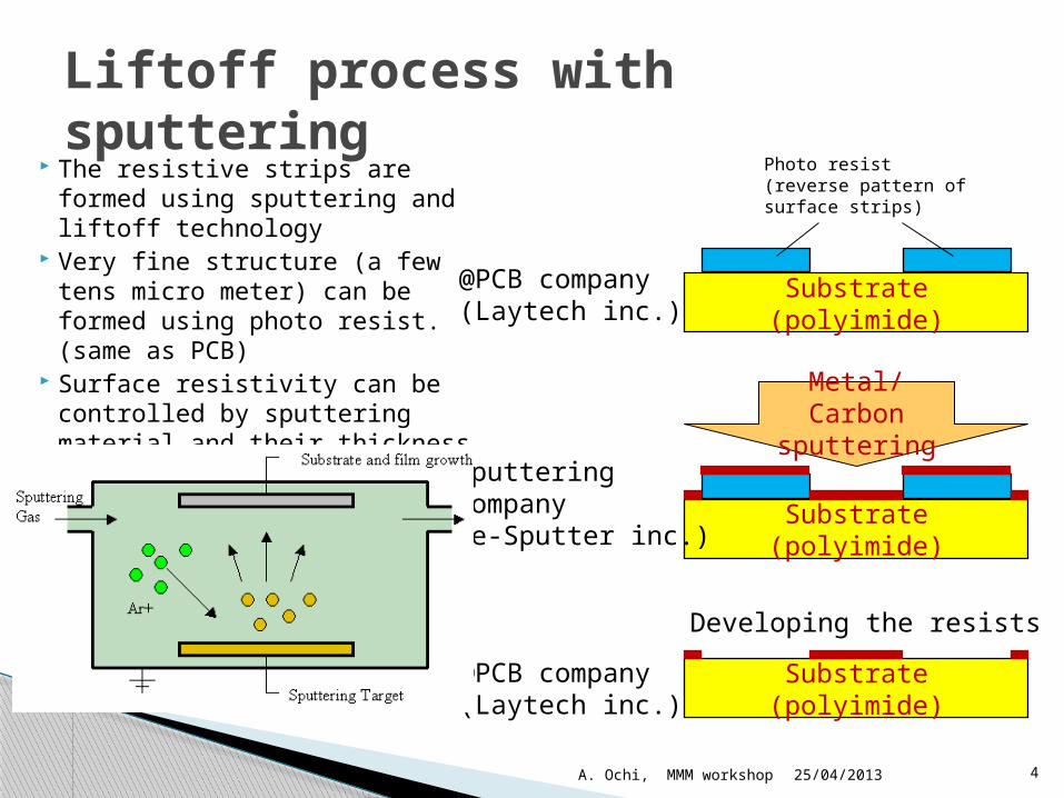
The resistive strips are formed using sputtering and liftoff technology
Very fine structure (a few tens micro meter) can be formed using photo resist. (same as PCB)
Surface resistivity can be controlled by sputtering material and their thickness
25/04/2013A. Ochi, MMM workshop 4
Liftoff process with sputtering
Substrate (polyimide)
Photo resist(reverse pattern of surface strips)
Substrate (polyimide)
Metal/Carbon
sputtering
Substrate (polyimide)
Developing the resists
@PCB company(Laytech inc.)
@Sputtering company(Be-Sputter inc.)
@PCB company(Laytech inc.)
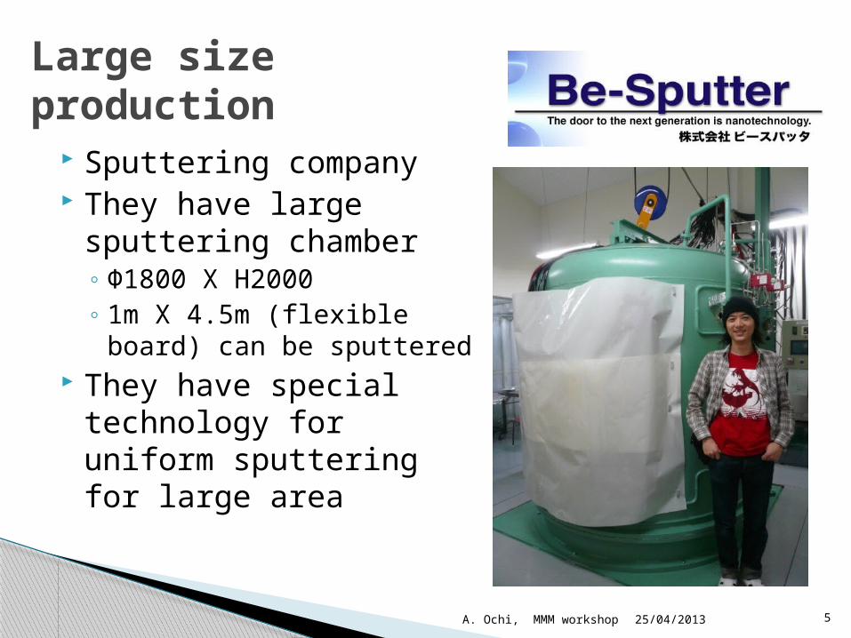
Sputtering company They have large
sputtering chamber◦ Φ1800 X H2000◦ 1m X 4.5m (flexible board)
can be sputtered They have special
technology for uniform sputtering for large area
Large size production
25/04/2013 5A. Ochi, MMM workshop
About sputtering micromegas First operation test for sputtering
micromegas. The mechanical structure ideas for large
size production Future plan
25/04/2013A. Ochi, MMM workshop 6
Outline
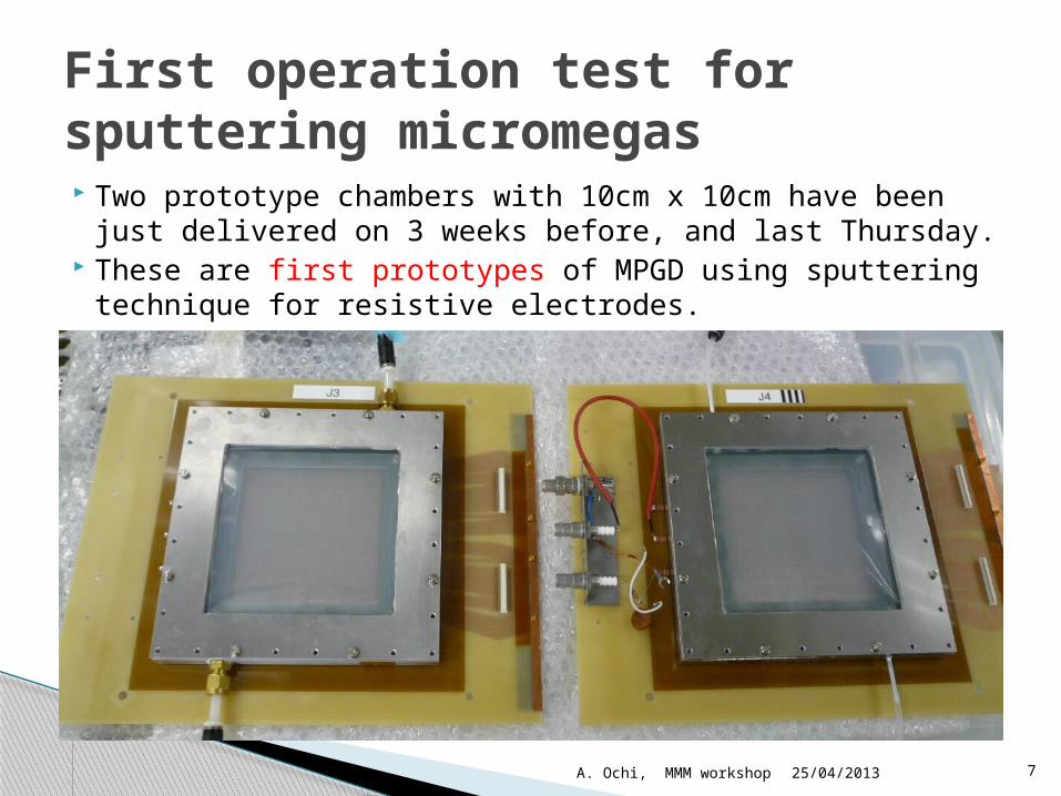
Two prototype chambers with 10cm x 10cm have been just delivered on 3 weeks before, and last Thursday.
These are first prototypes of MPGD using sputtering technique for resistive electrodes.
25/04/2013A. Ochi, MMM workshop 7
First operation test for sputtering micromegas
To confirm the detector operation using sputtering technologies◦ Most uncertain issue was, stability of ultra-thin resistive
strip (~ 300micron).◦ We should check whether small sparks and/or big pulse
destroy the electrodes or not. Using intense fast neutron, we can make big
pulses and sparks.◦ Also this condition is similar to ATLAS cavern.
The our first test for sputtering MM is the operation test under fast neutron.◦ Other properties, i.e. position/timing resolution, should be
checked. However, that stability test has top priority.
25/04/2013A. Ochi, MMM workshop 8
We should check…
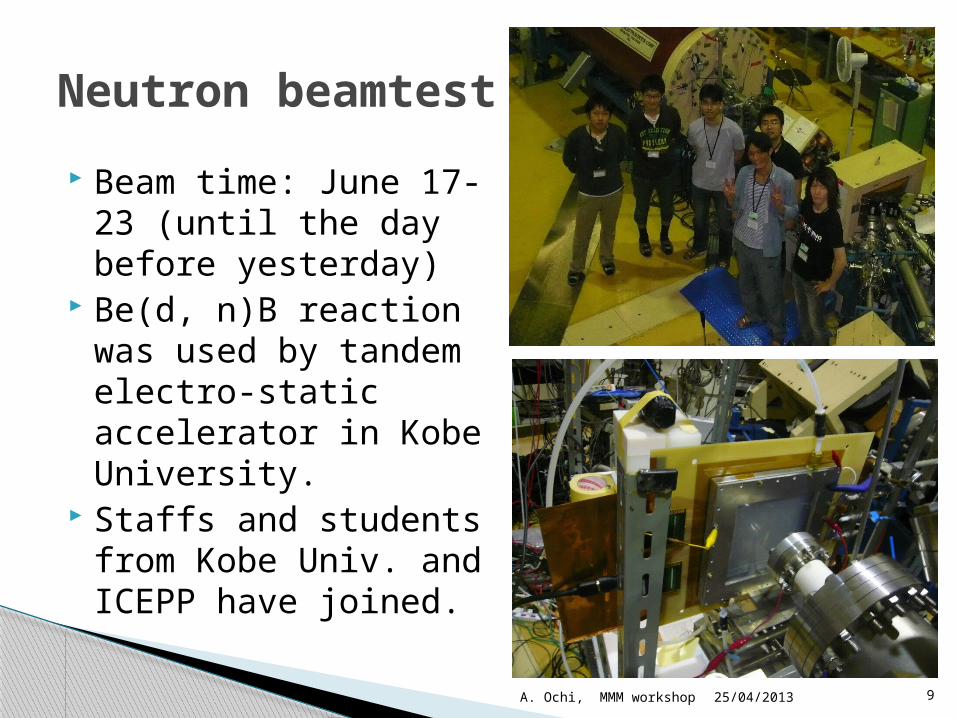
Beam time: June 17-23 (until the day before yesterday)
Be(d, n)B reaction was used by tandem electro-static accelerator in Kobe University.
Staffs and students from Kobe Univ. and ICEPP have joined.
25/04/2013A. Ochi, MMM workshop 9
Neutron beamtest
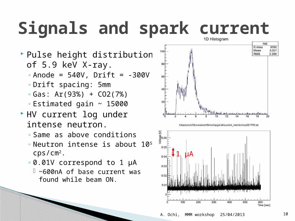
Pulse height distribution of 5.9 keV X-ray.◦ Anode = 540V, Drift = -300V◦ Drift spacing: 5mm◦ Gas: Ar(93%) + CO2(7%)◦ Estimated gain ~ 15000
HV current log under intense neutron.◦ Same as above conditions◦ Neutron intense is about 105
cps/cm2.◦ 0.01V correspond to 1 μA
~600nA of base current was found while beam ON.
25/04/2013A. Ochi, MMM workshop 10
Signals and spark current
1 μA
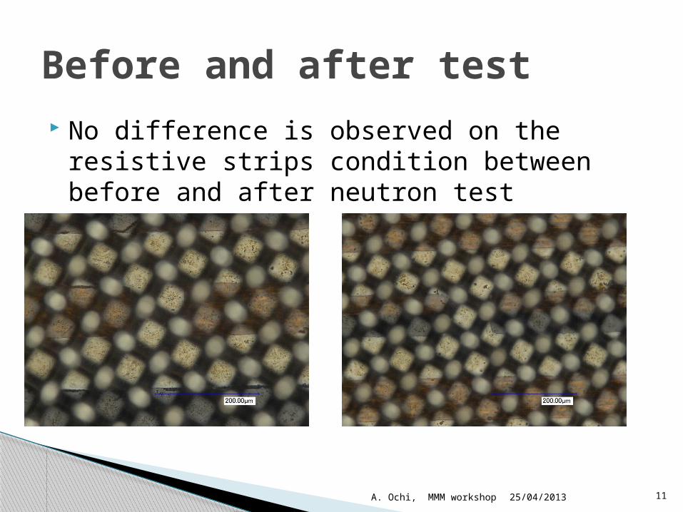
No difference is observed on the resistive strips condition between before and after neutron test
25/04/2013A. Ochi, MMM workshop 11
Before and after test
About sputtering micromegas First operation test for sputtering
micromegas. The mechanical structure ideas for large
size production Future plan
25/04/2013A. Ochi, MMM workshop 12
Outline
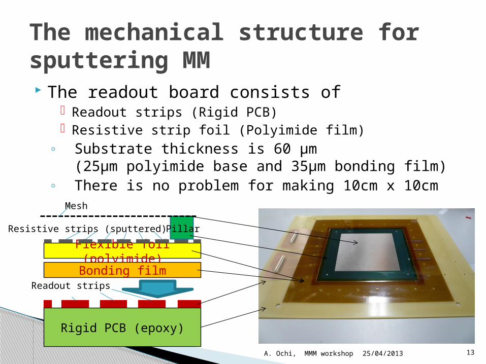
The readout board consists of Readout strips (Rigid PCB) Resistive strip foil (Polyimide film)
◦ Substrate thickness is 60 μm(25μm polyimide base and 35μm bonding film)
◦ There is no problem for making 10cm x 10cm
25/04/2013A. Ochi, MMM workshop 13
The mechanical structure for sputtering MM
Flexible foil (polyimide)
Rigid PCB (epoxy)
Resistive strips (sputtered)
Readout strips
Bonding film
Mesh
Pillar
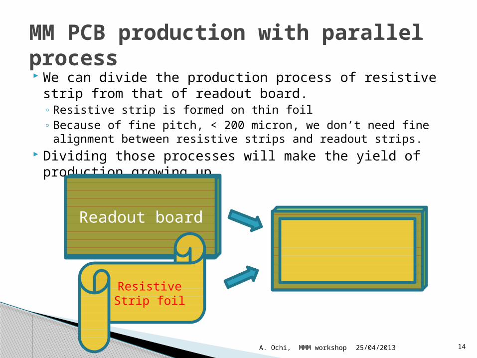
We can divide the production process of resistive strip from that of readout board.◦ Resistive strip is formed on thin foil◦ Because of fine pitch, < 200 micron, we don’t need fine
alignment between resistive strips and readout strips. Dividing those processes will make the yield of
production growing up.
25/04/2013A. Ochi, MMM workshop 14
MM PCB production with parallel process
Readout board
ResistiveStrip foil
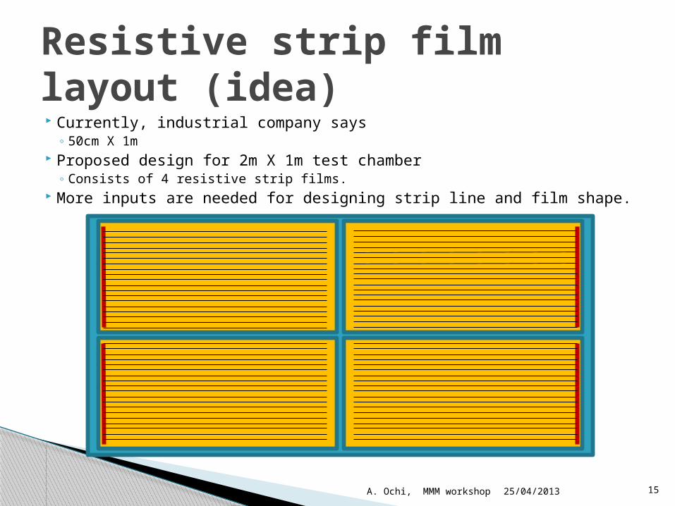
Currently, industrial company says ◦ 50cm X 1m
Proposed design for 2m X 1m test chamber◦ Consists of 4 resistive strip films.
More inputs are needed for designing strip line and film shape.
25/04/2013A. Ochi, MMM workshop 15
Resistive strip film layout (idea)
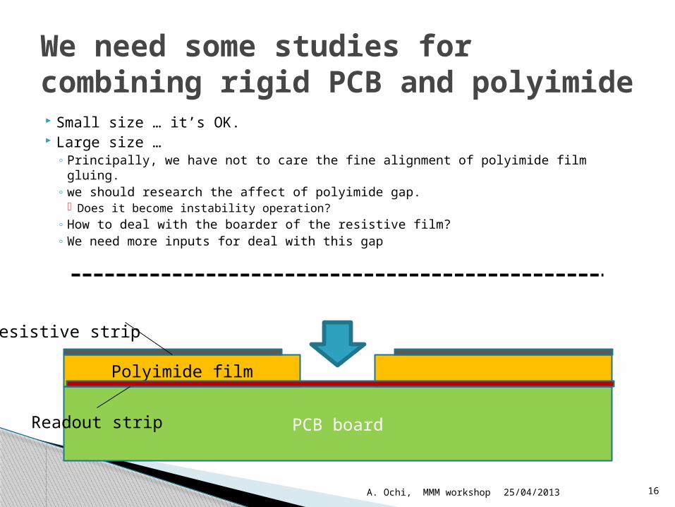
Small size … it’s OK. Large size …
◦ Principally, we have not to care the fine alignment of polyimide film gluing.◦ we should research the affect of polyimide gap.
Does it become instability operation? ◦ How to deal with the boarder of the resistive film?◦ We need more inputs for deal with this gap
25/04/2013A. Ochi, MMM workshop 16
We need some studies for combining rigid PCB and polyimide
PCB board
Polyimide film
Readout strip
Resistive strip
About sputtering micromegas First operation test for sputtering
micromegas. The mechanical structure ideas for large
size production Future plan
25/04/2013A. Ochi, MMM workshop 17
Outline
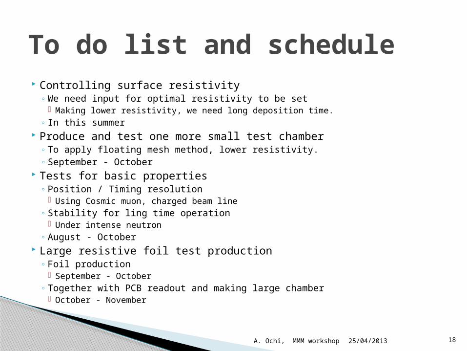
Controlling surface resistivity◦ We need input for optimal resistivity to be set
Making lower resistivity, we need long deposition time.◦ In this summer
Produce and test one more small test chamber◦ To apply floating mesh method, lower resistivity.◦ September - October
Tests for basic properties◦ Position / Timing resolution
Using Cosmic muon, charged beam line◦ Stability for ling time operation
Under intense neutron◦ August - October
Large resistive foil test production◦ Foil production
September - October◦ Together with PCB readout and making large chamber
October - November
25/04/2013A. Ochi, MMM workshop 18
To do list and schedule
We have operate sputtering MicroMEGAS successfully.
There is no defect after intense neutron operation.◦ Of course, We need more studies for longtime
operation and aging. The production process attaching rigid PCB
and polyimide film◦ For small chamber … no problem so far.◦ We need some idea for large size chamber.
25/04/2013A. Ochi, MMM workshop 19
Summary


![Dox 241 - Ochi pentru ochi [v.1.0].doc](https://img.pdfslide.net/doc/110x75/55cf885255034664618f6505/dox-241-ochi-pentru-ochi-v10doc.jpg)