Embed Size (px)
Citation preview
8-bit Microcontroller
Application Note
Rev. 2520B–AVR–07/03
AVR086: Replacing AT90S8535 by ATmega8535
Features• AT90S8535 Errata Corrected in ATmega8535• Changes to Names• Improvements to Timer/Counters and Prescalers• Improvements to the ADC• Improvements to SPI and UART• Changes to EEPROM Write Timing• Programming Interface• Fuse Settings• Oscillators and Selecting Start-up Delays• Changes to Watchdog Timer• Other Concerns• Features not Available in AT90S8535 Compatibility Mode
IntroductionThis application note is a guide to assist current AT90S8535 users in converting exist-ing designs to the ATmega8535. The ATmega8535 has two operating modes selectedthrough the fuse settings. The S8515C Fuse selects whether the AT90S8535 compat-ibility mode should be used or not. By default, the S8515C Fuse is unprogrammed andthe ATmega8535 does not operate in compatibility mode. When the compatibilitymode is used, only non-conflicting enhancements make the part different from theAT90S8535. Additionally, the electrical characteristics of the ATmega8535 are differ-ent including an increase in operating frequency because of a change in processtechnology. Check the data sheet for detailed information. When the S8515C Fuse isunprogrammed, all new features are supported, but porting the code may requiremore work.
AT90S8535 Errata Corrected in ATmega8535The following items from the Errata Sheets of the AT90S8535 do not apply to theATmega8535. Refer to the AT90S8535 Errata Sheet for a more detailed description ofthe errata.
Note: Some of these errata entries were corrected in the last revision of AT90S8535. Theyare still referred, to ease converting from any AT90S8535 design.
Releasing Reset Condition Without Clock
ATmega8535 has a new reset interface in which any External Reset Pulse exceedingthe minimum pulse width tRST causes an internal reset even though the condition dis-appears before any valid clock is present.
1

Incorrect Channel Changes in Free Running Mode
In ATmega8535, the MUXn and REFS1:0 bits in the ADMUX Register are bufferedthrough a temporary register to which the CPU has random access. This ensures thatthe channels and reference selection only takes place at a safe point during the conver-sion. Refer to the ATmega8535 data sheet for further information and advices on how tochange these registers in Free Running mode.
32 kHz Oscillator May Fail at Higher Voltages
In ATmega8535, the 32 kHz crystal Oscillator for Timer/Counter2 also works above4.0V. Refer to the ATmega8535 data sheet for electrical characteristics.
Incorrect Start-up Time The FSTRT Fuse in AT90S8535 is replaced by a more flexible system in ATmega8535,in which the fuses CKSEL3:0 and SUT1:0 selects clock source, frequency range, andStart-up times. Refer to the ATmega8535 data sheet for further information
Lock Bits at High VCC and Temperature
In ATmega8535, the Lock bits can be cleared over the full operating range.
Error in Half Carry Flag The Half Carry Flag works as expected in ATmega8535.
Error in Writing Reset Status Bits
The POR and XTRF Flag can be cleared individually in ATmega8535.
Wake-up from Sleep Executes Instructions before Interrupt is Serviced
ATmega8535 executes the Interrupt routine as the first instruction after wake-up fromPower-save mode.
If an enabled interrupt occurs while the ATmega8535 is in a sleep mode, the MCUwakes up. The MCU is then halted for four cycles, executes the interrupt routine, andresumes execution from the instruction following SLEEP.
SPI Can Send Wrong Byte In ATmega8535, a new byte can be written to the SPI Data Register on the same clockedge as the previous transfer finishes. There is no need to wait for the previous transferto complete before writing the next byte into the SPI Data Register when operating inMaster mode.
Output Compare Output Value Corrupted by Writing to Port
When OC1A and/or OC1B are used, writing to PORTD I/O location does not disturb theoperation of the compare pins.
Serial Programming at Voltages Below 3.4V
There are no restrictions on the supply voltage or system frequency as long as thedevice is operated inside the voltage and frequency range prescribed in the data sheetfor the ATmega8535.
Wake-up from Power-save without Global Interrupt Enable
Asynchronous Timer/Counter interrupts do not wake-up the part unless global interruptsare enabled in ATmega8535
UART Looses Synchronization if RXD Line is Low when UART Receive is Disabled
The UART is replaced with a USART, which does not have this problem. The startingedge of a reception is only accepted as valid if the Receive Enable bit in the USARTControl Register is set.
High Current Consumption at High VCC
ATmega8535 has the electrical characteristics described in its data sheet.
Leakage Current on Tri-stated I/O Pins
ATmega8535 has the electrical characteristics described in its data sheet.
2 AVR0862520B–AVR–07/03
AVR086
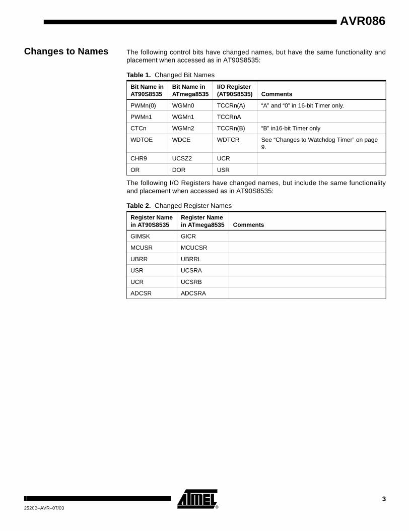
Changes to Names The following control bits have changed names, but have the same functionality andplacement when accessed as in AT90S8535:
The following I/O Registers have changed names, but include the same functionalityand placement when accessed as in AT90S8535:
Table 1. Changed Bit Names
Bit Name inAT90S8535
Bit Name inATmega8535
I/O Register(AT90S8535) Comments
PWMn(0) WGMn0 TCCRn(A) “A” and “0” in 16-bit Timer only.
PWMn1 WGMn1 TCCRnA
CTCn WGMn2 TCCRn(B) “B” in16-bit Timer only
WDTOE WDCE WDTCR See “Changes to Watchdog Timer” on page 9.
CHR9 UCSZ2 UCR
OR DOR USR
Table 2. Changed Register Names
Register Namein AT90S8535
Register Namein ATmega8535 Comments
GIMSK GICR
MCUSR MCUCSR
UBRR UBRRL
USR UCSRA
UCR UCSRB
ADCSR ADCSRA
32520B–AVR–07/03
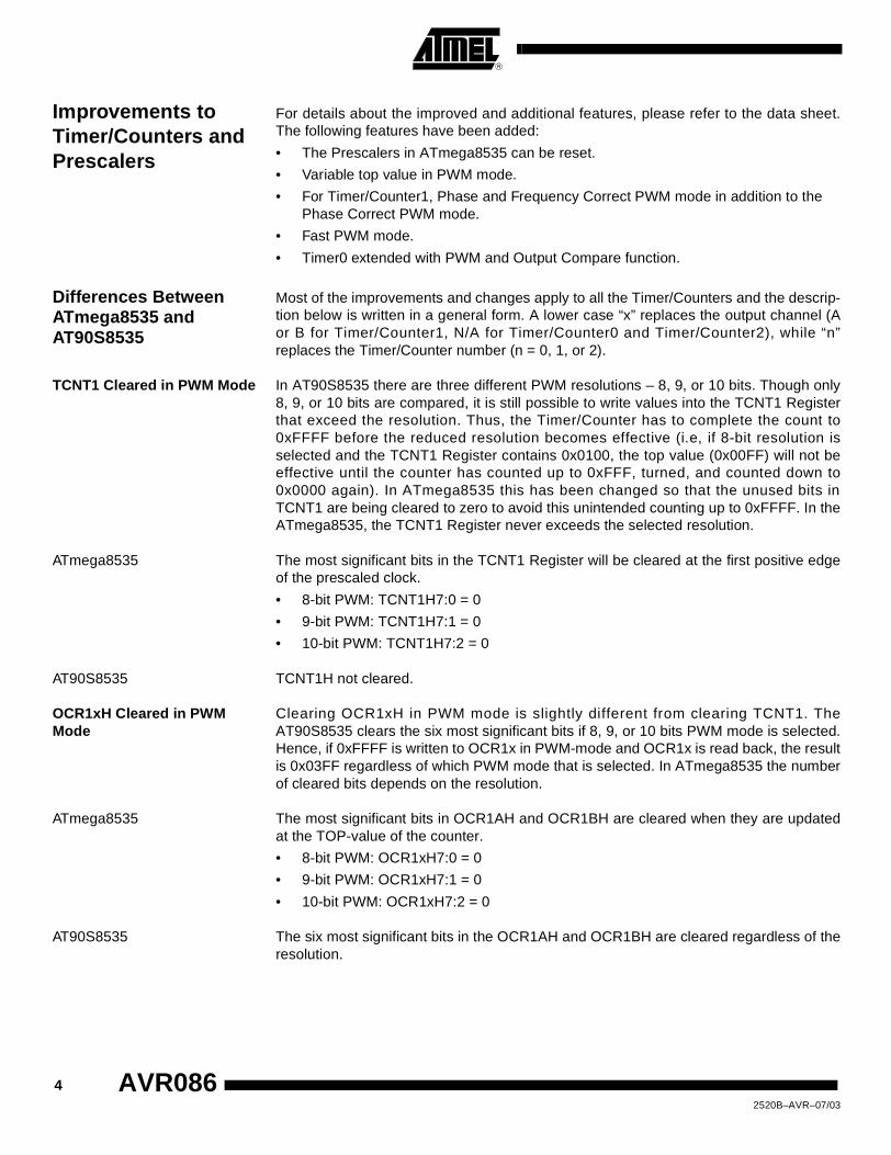
Improvements to Timer/Counters and Prescalers
For details about the improved and additional features, please refer to the data sheet.The following features have been added:
• The Prescalers in ATmega8535 can be reset.
• Variable top value in PWM mode.
• For Timer/Counter1, Phase and Frequency Correct PWM mode in addition to the Phase Correct PWM mode.
• Fast PWM mode.
• Timer0 extended with PWM and Output Compare function.
Differences Between ATmega8535 and AT90S8535
Most of the improvements and changes apply to all the Timer/Counters and the descrip-tion below is written in a general form. A lower case “x” replaces the output channel (Aor B for Timer/Counter1, N/A for Timer/Counter0 and Timer/Counter2), while “n”replaces the Timer/Counter number (n = 0, 1, or 2).
TCNT1 Cleared in PWM Mode In AT90S8535 there are three different PWM resolutions – 8, 9, or 10 bits. Though only8, 9, or 10 bits are compared, it is still possible to write values into the TCNT1 Registerthat exceed the resolution. Thus, the Timer/Counter has to complete the count to0xFFFF before the reduced resolution becomes effective (i.e, if 8-bit resolution isselected and the TCNT1 Register contains 0x0100, the top value (0x00FF) will not beeffective until the counter has counted up to 0xFFF, turned, and counted down to0x0000 again). In ATmega8535 this has been changed so that the unused bits inTCNT1 are being cleared to zero to avoid this unintended counting up to 0xFFFF. In theATmega8535, the TCNT1 Register never exceeds the selected resolution.
ATmega8535 The most significant bits in the TCNT1 Register will be cleared at the first positive edgeof the prescaled clock.
• 8-bit PWM: TCNT1H7:0 = 0
• 9-bit PWM: TCNT1H7:1 = 0
• 10-bit PWM: TCNT1H7:2 = 0
AT90S8535 TCNT1H not cleared.
OCR1xH Cleared in PWM Mode
Clearing OCR1xH in PWM mode is slightly different from clearing TCNT1. TheAT90S8535 clears the six most significant bits if 8, 9, or 10 bits PWM mode is selected.Hence, if 0xFFFF is written to OCR1x in PWM-mode and OCR1x is read back, the resultis 0x03FF regardless of which PWM mode that is selected. In ATmega8535 the numberof cleared bits depends on the resolution.
ATmega8535 The most significant bits in OCR1AH and OCR1BH are cleared when they are updatedat the TOP-value of the counter.
• 8-bit PWM: OCR1xH7:0 = 0
• 9-bit PWM: OCR1xH7:1 = 0
• 10-bit PWM: OCR1xH7:2 = 0
AT90S8535 The six most significant bits in the OCR1AH and OCR1BH are cleared regardless of theresolution.
4 AVR0862520B–AVR–07/03
AVR086
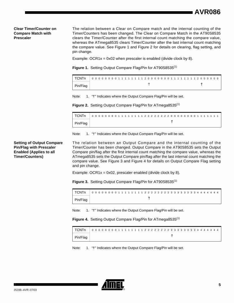
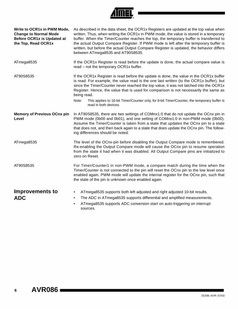
Clear Timer/Counter on Compare Match with Prescaler
The relation between a Clear on Compare match and the internal counting of theTimer/Counters has been changed. The Clear on Compare Match in the AT90S8535clears the Timer/Counter after the first internal count matching the compare value,whereas the ATmega8535 clears Timer/Counter after the last internal count matchingthe compare value. See Figure 1 and Figure 2 for details on clearing, flag setting, andpin change.
Example: OCR1x = 0x02 when prescaler is enabled (divide clock by 8).
Figure 1. Setting Output Compare Flag/Pin for AT90S8535(1)
Note: 1. “�” Indicates where the Output Compare Flag/Pin will be set.
Figure 2. Setting Output Compare Flag/Pin for ATmega8535(1)
Note: 1. “�” Indicates where the Output Compare Flag/Pin will be set.
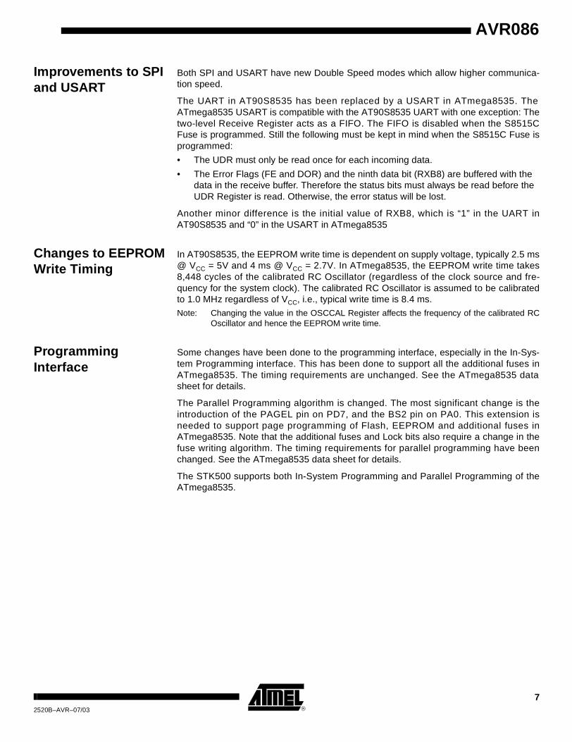
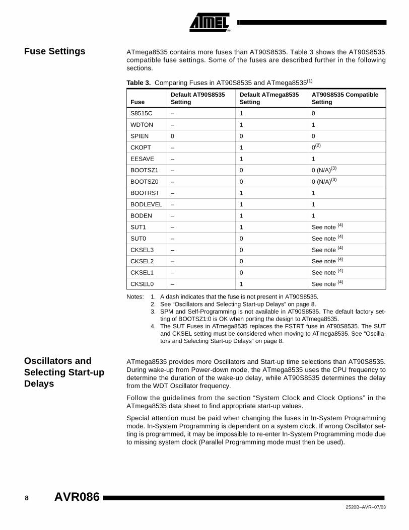
Setting of Output Compare Pin/Flag with Prescaler Enabled (Applies to all Timer/Counters)
The relation between an Output Compare and the internal counting of theTimer/Counter has been changed. Output Compare in the AT90S8535 sets the OutputCompare pin/flag after the first internal count matching the compare value, whereas theATmega8535 sets the Output Compare pin/flag after the last internal count matching thecompare value. See Figure 3 and Figure 4 for details on Output Compare Flag settingand pin change.
Example: OCR1x = 0x02, prescaler enabled (divide clock by 8).
Figure 3. Setting Output Compare Flag/Pin for AT90S8535(1)
Note: 1. “�” Indicates where the Output Compare Flag/Pin will be set.
Figure 4. Setting Output Compare Flag/Pin for ATmega8535(1)
Note: 1. “�” Indicates where the Output Compare Flag/Pin will be set.
TCNTn 0 0 0 0 0 0 0 0 1 1 1 1 1 1 1 1 2 0 0 0 0 0 0 0 1 1 1 1 1 1 1 1 2 0 0 0 0 0 0
Pin/Flag � �
TCNTn 0 0 0 0 0 0 0 0 1 1 1 1 1 1 1 1 2 2 2 2 2 2 2 2 0 0 0 0 0 0 0 0 1 1 1 1 1 1 1
Pin/Flag �
TCNTn 0 0 0 0 0 0 0 0 1 1 1 1 1 1 1 1 2 2 2 2 2 2 2 2 3 3 3 3 3 3 3 3 4 4 4 4 4 4 4
Pin/Flag �
TCNTn 0 0 0 0 0 0 0 0 1 1 1 1 1 1 1 1 2 2 2 2 2 2 2 2 3 3 3 3 3 3 3 3 4 4 4 4 4 4 4
Pin/Flag �
52520B–AVR–07/03
Write to OCR1x in PWM Mode, Change to Normal Mode Before OCR1x is Updated at the Top, Read OCR1x
As described in the data sheet, the OCR1x Registers are updated at the top value whenwritten. Thus, when writing the OCR1x in PWM mode, the value is stored in a temporarybuffer. When the Timer/Counter reaches the top, the temporary buffer is transferred tothe actual Output Compare Register. If PWM mode is left after the temporary buffer iswritten, but before the actual Output Compare Register is updated, the behavior differsbetween ATmega8535 and AT90S8535.
ATmega8535 If the OCR1x Register is read before the update is done, the actual compare value isread – not the temporary OCR1x buffer.
AT90S8535 If the OCR1x Register is read before the update is done, the value in the OCR1x bufferis read. For example, the value read is the one last written (to the OCR1x buffer), butsince the Timer/Counter never reached the top value, it was not latched into the OCR1xRegister. Hence, the value that is used for comparison is not necessarily the same asbeing read.
Note: This applies to 16-bit Timer/Counter only, for 8-bit Timer/Counter, the temporary buffer isread in both devices.
Memory of Previous OCnx pin Level
In AT90S8535, there are two settings of COMnx1:0 that do not update the OCnx pin inPWM mode (0b00 and 0b01), and one setting of COMnx1:0 in non-PWM mode (0b00).Assume the Timer/Counter is taken from a state that updates the OCnx pin to a statethat does not, and then back again to a state that does update the OCnx pin. The follow-ing differences should be noted:
ATmega8535 The level of the OCnx-pin before disabling the Output Compare mode is remembered.Re-enabling the Output Compare mode will cause the OCnx pin to resume operationfrom the state it had when it was disabled. All Output Compare pins are initialized tozero on Reset.
AT90S8535 For Timer/Counter1 in non-PWM mode, a compare match during the time when theTimer/Counter is not connected to the pin will reset the OCnx pin to the low level onceenabled again. PWM mode will update the internal register for the OCnx pin, such thatthe state of the pin is unknown once enabled again.
Improvements to ADC
• ATmega8535 supports both left adjusted and right adjusted 10-bit results.
• The ADC in ATmega8535 supports differential and amplified measurements.
• ATmega8535 supports ADC conversion start on auto-triggering on interrupt sources.
6 AVR0862520B–AVR–07/03
AVR086
Improvements to SPI and USART
Both SPI and USART have new Double Speed modes which allow higher communica-tion speed.
The UART in AT90S8535 has been replaced by a USART in ATmega8535. TheATmega8535 USART is compatible with the AT90S8535 UART with one exception: Thetwo-level Receive Register acts as a FIFO. The FIFO is disabled when the S8515CFuse is programmed. Still the following must be kept in mind when the S8515C Fuse isprogrammed:
• The UDR must only be read once for each incoming data.
• The Error Flags (FE and DOR) and the ninth data bit (RXB8) are buffered with the data in the receive buffer. Therefore the status bits must always be read before the UDR Register is read. Otherwise, the error status will be lost.
Another minor difference is the initial value of RXB8, which is “1” in the UART inAT90S8535 and “0” in the USART in ATmega8535
Changes to EEPROM Write Timing
In AT90S8535, the EEPROM write time is dependent on supply voltage, typically 2.5 ms@ VCC = 5V and 4 ms @ VCC = 2.7V. In ATmega8535, the EEPROM write time takes8,448 cycles of the calibrated RC Oscillator (regardless of the clock source and fre-quency for the system clock). The calibrated RC Oscillator is assumed to be calibratedto 1.0 MHz regardless of VCC, i.e., typical write time is 8.4 ms.
Note: Changing the value in the OSCCAL Register affects the frequency of the calibrated RCOscillator and hence the EEPROM write time.
Programming Interface
Some changes have been done to the programming interface, especially in the In-Sys-tem Programming interface. This has been done to support all the additional fuses inATmega8535. The timing requirements are unchanged. See the ATmega8535 datasheet for details.
The Parallel Programming algorithm is changed. The most significant change is theintroduction of the PAGEL pin on PD7, and the BS2 pin on PA0. This extension isneeded to support page programming of Flash, EEPROM and additional fuses inATmega8535. Note that the additional fuses and Lock bits also require a change in thefuse writing algorithm. The timing requirements for parallel programming have beenchanged. See the ATmega8535 data sheet for details.
The STK500 supports both In-System Programming and Parallel Programming of theATmega8535.
72520B–AVR–07/03
Fuse Settings ATmega8535 contains more fuses than AT90S8535. Table 3 shows the AT90S8535compatible fuse settings. Some of the fuses are described further in the followingsections.
Notes: 1. A dash indicates that the fuse is not present in AT90S8535.2. See “Oscillators and Selecting Start-up Delays” on page 8.3. SPM and Self-Programming is not available in AT90S8535. The default factory set-
ting of BOOTSZ1:0 is OK when porting the design to ATmega8535.4. The SUT Fuses in ATmega8535 replaces the FSTRT fuse in AT90S8535. The SUT
and CKSEL setting must be considered when moving to ATmega8535. See “Oscilla-tors and Selecting Start-up Delays” on page 8.
Oscillators and Selecting Start-up Delays
ATmega8535 provides more Oscillators and Start-up time selections than AT90S8535.During wake-up from Power-down mode, the ATmega8535 uses the CPU frequency todetermine the duration of the wake-up delay, while AT90S8535 determines the delayfrom the WDT Oscillator frequency.
Follow the guidelines from the section “System Clock and Clock Options” in theATmega8535 data sheet to find appropriate start-up values.
Special attention must be paid when changing the fuses in In-System Programmingmode. In-System Programming is dependent on a system clock. If wrong Oscillator set-ting is programmed, it may be impossible to re-enter In-System Programming mode dueto missing system clock (Parallel Programming mode must then be used).
Table 3. Comparing Fuses in AT90S8535 and ATmega8535(1)
FuseDefault AT90S8535 Setting
Default ATmega8535 Setting
AT90S8535 Compatible Setting
S8515C – 1 0
WDTON – 1 1
SPIEN 0 0 0
CKOPT – 1 0(2)
EESAVE – 1 1
BOOTSZ1 – 0 0 (N/A)(3)
BOOTSZ0 – 0 0 (N/A)(3)
BOOTRST – 1 1
BODLEVEL – 1 1
BODEN – 1 1
SUT1 – 1 See note (4)
SUT0 – 0 See note (4)
CKSEL3 – 0 See note (4)
CKSEL2 – 0 See note (4)
CKSEL1 – 0 See note (4)
CKSEL0 – 1 See note (4)
8 AVR0862520B–AVR–07/03
AVR086
The crystal oscillator in AT90S8535 is capable of driving an addition clock buffer fromthe XTAL2 output. In ATmega8535, this is only possible when the CKOPT Fuse is pro-grammed. In this mode the Oscillator has a rail-to-rail swing at the output, but at theexpense of higher power consumption. Hence, do only program this fuse when rail-to-rail swing is required.
Changes to Watchdog Timer
The Watchdog Timer in ATmega8535 is improved compared to the one in AT90S8535.In AT90S8535, the Watchdog Timer is either enabled or disabled, while ATmega8535supports two safety levels selected by the WDTON Fuse. See description inATmega8535 data sheet for further information.
The combination of programming the S8515C Fuse and having the WDTON Fuseunprogrammed makes the Watchdog Timer behave exactly as in AT90S8535.
The frequency of the Watchdog Oscillator in ATmega8535 is close to 1.0 MHz for allsupply voltages. The typical frequency of the Watchdog Oscillator in AT90S8535 isclose to 1.0 MHz at 5V, but the Time-out period increases with decreasing VCC. Thismeans that the selection of Time-out period for the Watchdog Timer (in terms of numberof WDT Oscil lator cycles) must be reconsidered when porting the design toATmega8535. Refer to the data sheet for ATmega8535 for further information.
Other Concerns The ATmega8535 has a Signature Byte different from the one used in AT90S8535.Make sure you are using the Signature Byte of ATmega8535 when porting the design.
Be aware that EEPROM write access must be completed before entering power-downsleep mode. Otherwise the system oscillator will continue to run, drawing additionalcurrent.
Features not Available in AT90S8535 Compatibility Mode
The cS8515C Fuse makes the ATmega8535 compatible to AT90S8535. However, withthe S8515C Fuse programmed, some of the new features in ATmega8535 becomeunavailable. The following features are not supported when the ATmega8535 is used inthe AT90S8535 compatibility mode:
• The FIFO operation of the USART.
• Access to the status bits WDRF and BORF in MCUCSR.
• A timed sequence to change Watchdog Timer prescaler settings by software.
• External Interrupt INT2. The INT2 bit in the General Interrupt Control Register – GICR – cannot be written to one, and the INT2 bit in General Interrupt Flag Register – GIRF – will always read as zero.
• Compare function of Timer/Counter0. The OCIE0 bit in the Timer Interrupt Mask Register – TIMSK – cannot be written to one, and the OCIF0 bit in the Timer Interrupt Flag Register – TIFR – will always read as zero.
If any of the features above are needed or wanted and the S8515C Fuse is unpro-grammed, this introduces some differences between ATmega8535 and AT90S8535which do not exist as long as the compatibility fuse is programmed:
• A timed sequence must be followed to change Watchdog Timer prescaler settings by software.
• In the MCUCSR Register, all RESET Flags are present in the register, not only EXTRF and PORF as in AT90S8535.
• The UART will have an extra input buffer which allows one more data byte to be received before the Data OverRun Flag (DOR) is set.
92520B–AVR–07/03
Printed on recycled paper.
Disclaimer: Atmel Corporation makes no warranty for the use of its products, other than those expressly contained in the Company’s standardwarranty which is detailed in Atmel’s Terms and Conditions located on the Company’s web site. The Company assumes no responsibility for anyerrors which may appear in this document, reserves the right to change devices or specifications detailed herein at any time without notice, anddoes not make any commitment to update the information contained herein. No licenses to patents or other intellectual property of Atmel aregranted by the Company in connection with the sale of Atmel products, expressly or by implication. Atmel’s products are not authorized for useas critical components in life support devices or systems.
Atmel Corporation Atmel Operations
2325 Orchard ParkwaySan Jose, CA 95131Tel: 1(408) 441-0311Fax: 1(408) 487-2600
Regional Headquarters
EuropeAtmel SarlRoute des Arsenaux 41Case Postale 80CH-1705 FribourgSwitzerlandTel: (41) 26-426-5555Fax: (41) 26-426-5500
AsiaRoom 1219Chinachem Golden Plaza77 Mody Road TsimshatsuiEast KowloonHong KongTel: (852) 2721-9778Fax: (852) 2722-1369
Japan9F, Tonetsu Shinkawa Bldg.1-24-8 ShinkawaChuo-ku, Tokyo 104-0033JapanTel: (81) 3-3523-3551Fax: (81) 3-3523-7581
Memory2325 Orchard ParkwaySan Jose, CA 95131Tel: 1(408) 441-0311Fax: 1(408) 436-4314
Microcontrollers2325 Orchard ParkwaySan Jose, CA 95131Tel: 1(408) 441-0311Fax: 1(408) 436-4314
La ChantrerieBP 7060244306 Nantes Cedex 3, FranceTel: (33) 2-40-18-18-18Fax: (33) 2-40-18-19-60
ASIC/ASSP/Smart CardsZone Industrielle13106 Rousset Cedex, FranceTel: (33) 4-42-53-60-00Fax: (33) 4-42-53-60-01
1150 East Cheyenne Mtn. Blvd.Colorado Springs, CO 80906Tel: 1(719) 576-3300Fax: 1(719) 540-1759
Scottish Enterprise Technology ParkMaxwell BuildingEast Kilbride G75 0QR, Scotland Tel: (44) 1355-803-000Fax: (44) 1355-242-743
RF/AutomotiveTheresienstrasse 2Postfach 353574025 Heilbronn, GermanyTel: (49) 71-31-67-0Fax: (49) 71-31-67-2340
1150 East Cheyenne Mtn. Blvd.Colorado Springs, CO 80906Tel: 1(719) 576-3300Fax: 1(719) 540-1759
Biometrics/Imaging/Hi-Rel MPU/High Speed Converters/RF Datacom
Avenue de RochepleineBP 12338521 Saint-Egreve Cedex, FranceTel: (33) 4-76-58-30-00Fax: (33) 4-76-58-34-80
Web Sitehttp://www.atmel.com
2520B–AVR–07/03 0M
© Atmel Corporation 2003. All rights reserved. Atmel® and combinations thereof, AVR® and AVR Studio®
are the registered trademarks of Atmel Corporation or its subsidiaries.
Other terms and product names may be the trademarks of others.