Embed Size (px)
Citation preview
1
Basic Processor Architecture
2
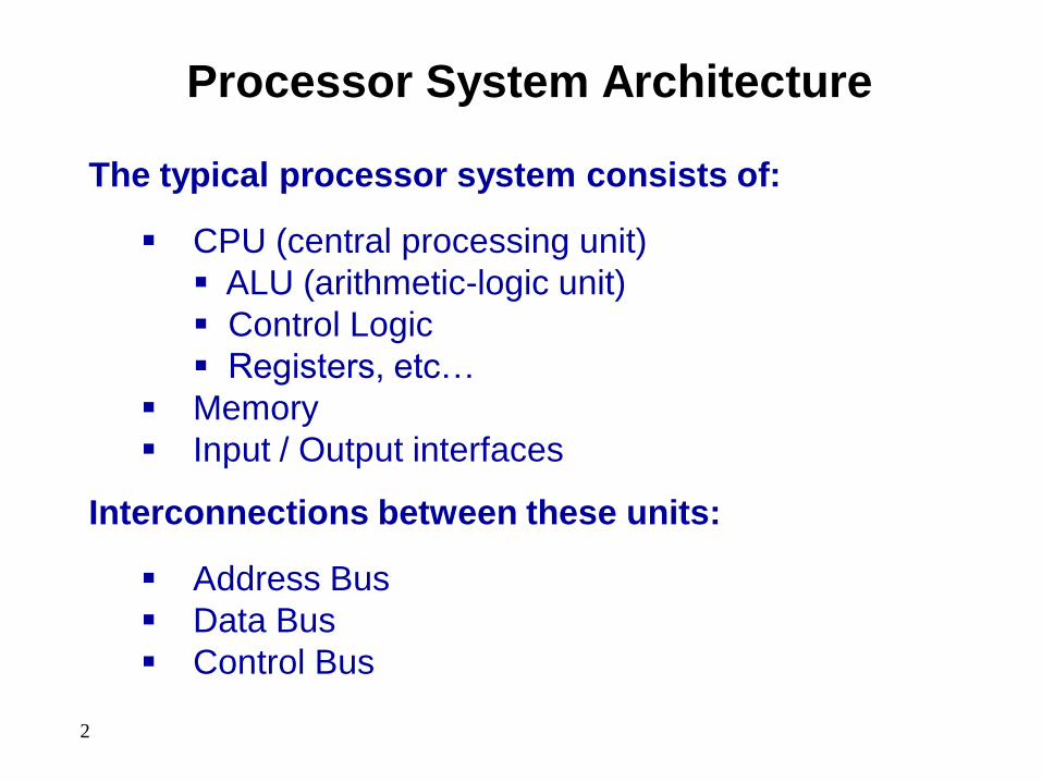
Processor System Architecture
The typical processor system consists of:
CPU (central processing unit)
ALU (arithmetic-logic unit)
Control Logic
Registers, etc…
Memory
Input / Output interfaces
Interconnections between these units:
Address Bus
Data Bus
Control Bus
3
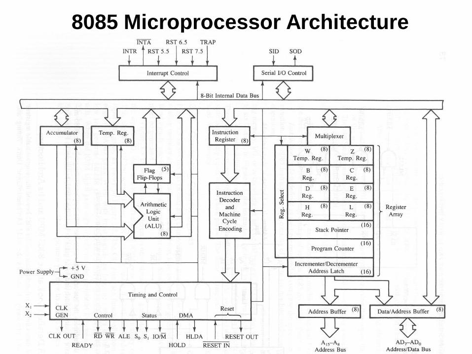
8085 Microprocessor Architecture
4
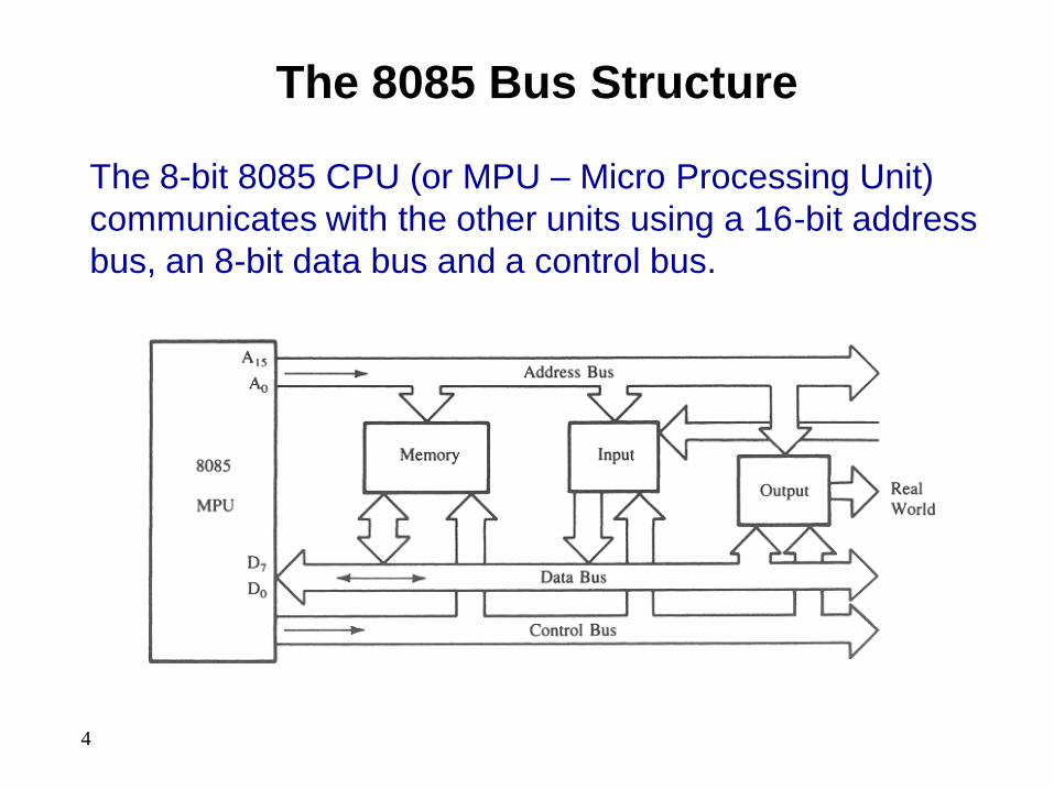
The 8085 Bus Structure
The 8-bit 8085 CPU (or MPU – Micro Processing Unit)
communicates with the other units using a 16-bit address
bus, an 8-bit data bus and a control bus.
5
The 8085 Bus Structure
Address Bus
Consists of 16 address lines: A0 – A15
Operates in unidirectional mode: The address
bits are always sent from the MPU to peripheral
devices, not reverse.
16 address lines are capable of addressing a
total of 216 = 65,536 (64k) memory locations.
Address locations: 0000 (hex) – FFFF (hex)
6
The 8085 Bus Structure
Data Bus
Consists of 8 data lines: D0 – D7
Operates in bidirectional mode: The data bits are
sent from the MPU to peripheral devices, as well
as from the peripheral devices to the MPU.
Data range: 00 (hex) – FF (hex)
Control Bus
Consists of various lines carrying the control
signals such as read / write enable, flag bits.
7
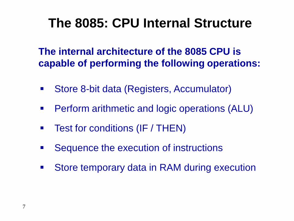
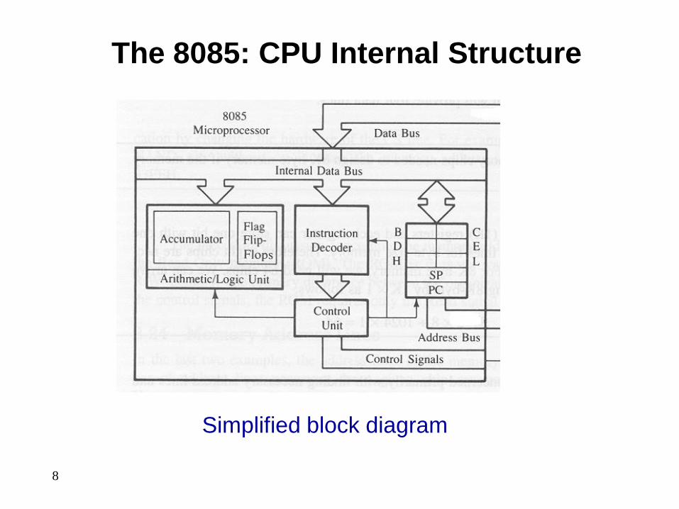
The 8085: CPU Internal Structure
The internal architecture of the 8085 CPU is
capable of performing the following operations:
Store 8-bit data (Registers, Accumulator)
Perform arithmetic and logic operations (ALU)
Test for conditions (IF / THEN)
Sequence the execution of instructions
Store temporary data in RAM during execution
8
The 8085: CPU Internal Structure
Simplified block diagram
9
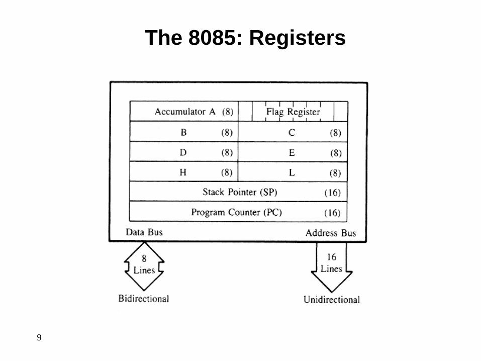
The 8085: Registers
10
The 8085: CPU Internal Structure
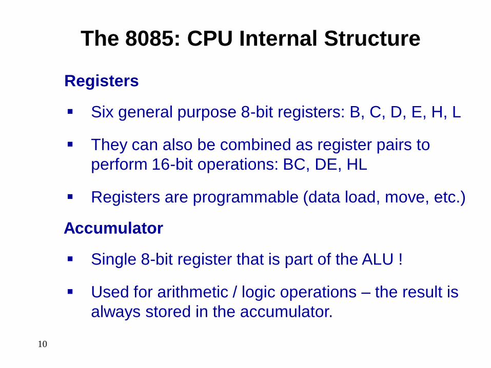
Registers
Six general purpose 8-bit registers: B, C, D, E, H, L
They can also be combined as register pairs to
perform 16-bit operations: BC, DE, HL
Registers are programmable (data load, move, etc.)
Accumulator
Single 8-bit register that is part of the ALU !
Used for arithmetic / logic operations – the result is
always stored in the accumulator.
11
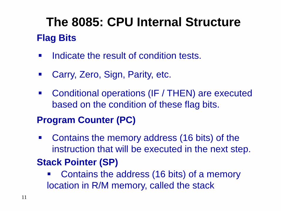
The 8085: CPU Internal Structure
Flag Bits
Indicate the result of condition tests.
Carry, Zero, Sign, Parity, etc.
Conditional operations (IF / THEN) are executed
based on the condition of these flag bits.
Program Counter (PC)
Contains the memory address (16 bits) of the
instruction that will be executed in the next step.
Stack Pointer (SP)
Contains the address (16 bits) of a memory
location in R/M memory, called the stack
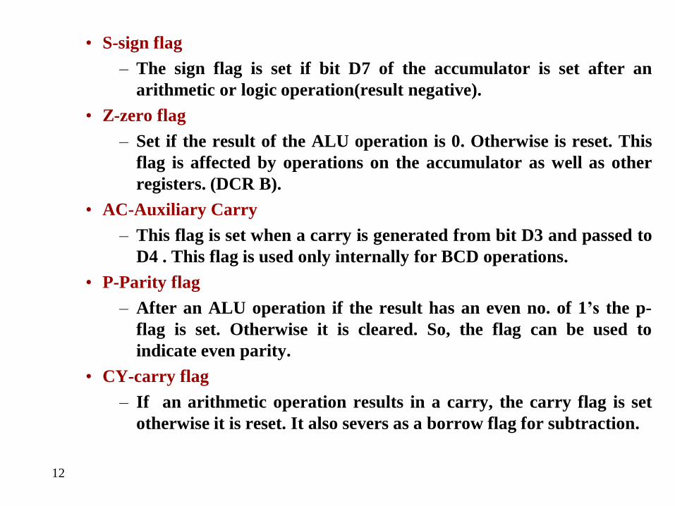
• S-sign flag
– The sign flag is set if bit D7 of the accumulator is set after an
arithmetic or logic operation(result negative).
• Z-zero flag
– Set if the result of the ALU operation is 0. Otherwise is reset. This
flag is affected by operations on the accumulator as well as other
registers. (DCR B).
• AC-Auxiliary Carry
– This flag is set when a carry is generated from bit D3 and passed to
D4 . This flag is used only internally for BCD operations.
• P-Parity flag
– After an ALU operation if the result has an even no. of 1’s the p-
flag is set. Otherwise it is cleared. So, the flag can be used to
indicate even parity.
• CY-carry flag
– If an arithmetic operation results in a carry, the carry flag is set
otherwise it is reset. It also severs as a borrow flag for subtraction.
12
13
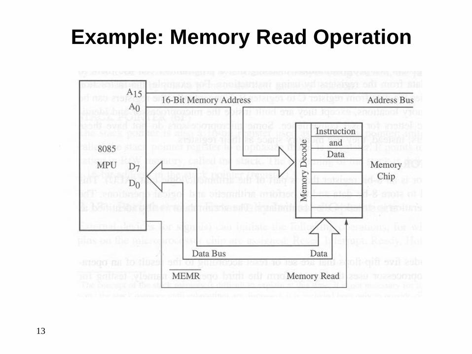
Example: Memory Read Operation
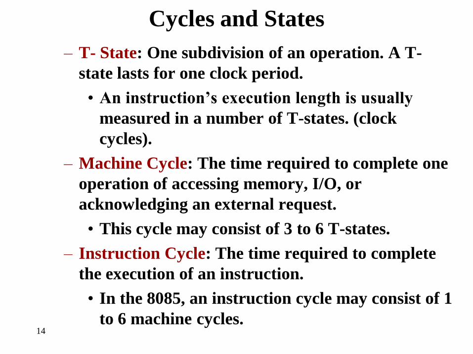
Cycles and States
– T- State: One subdivision of an operation. A T-
state lasts for one clock period.
• An instruction’s execution length is usually
measured in a number of T-states. (clock
cycles).
– Machine Cycle: The time required to complete one
operation of accessing memory, I/O, or
acknowledging an external request.
• This cycle may consist of 3 to 6 T-states.
– Instruction Cycle: The time required to complete
the execution of an instruction.
• In the 8085, an instruction cycle may consist of 1
to 6 machine cycles.14
15
• The 8085 executes several types of instructions
with each requiring a different number of
operations of different types. However, the
operations can be grouped into a small set.
• The three main types are:
• Memory Read and Write.
• I/O Read and Write.
• Request Acknowledge.
• These can be further divided into various
operations (machine cycles).
16
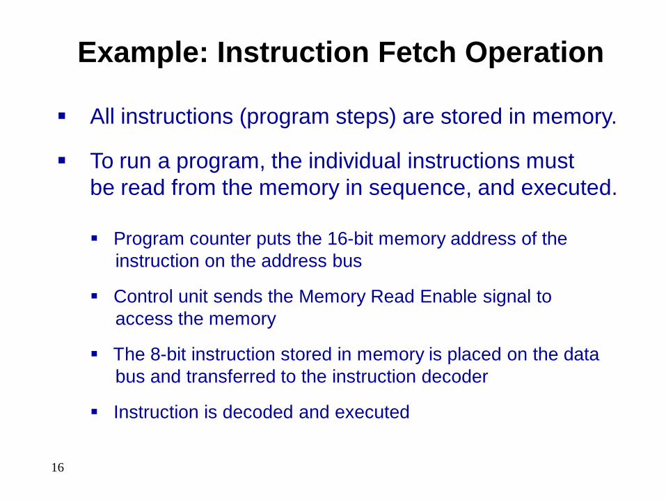
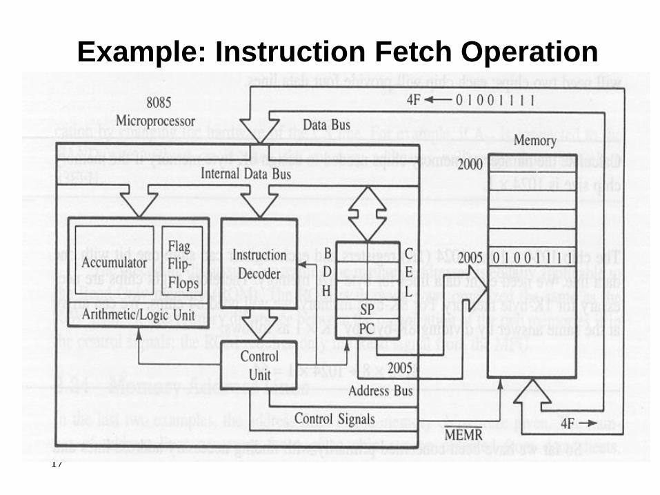
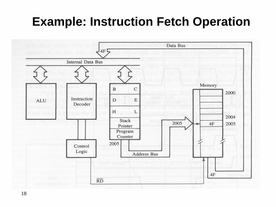
Example: Instruction Fetch Operation
All instructions (program steps) are stored in memory.
To run a program, the individual instructions must
be read from the memory in sequence, and executed.
Program counter puts the 16-bit memory address of the
instruction on the address bus
Control unit sends the Memory Read Enable signal to
access the memory
The 8-bit instruction stored in memory is placed on the data
bus and transferred to the instruction decoder
Instruction is decoded and executed
17
Example: Instruction Fetch Operation
18
Example: Instruction Fetch Operation
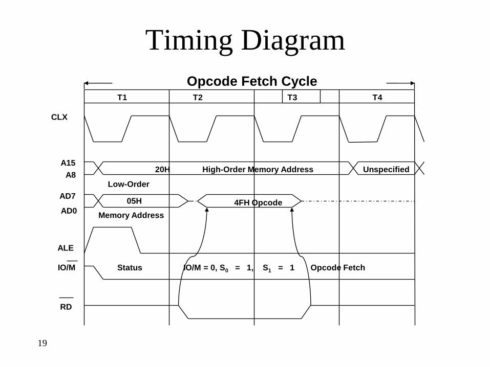
Timing Diagram
19
T1 T2 T3 T4
CLX
Opcode Fetch Cycle
A15
A8
AD7
AD0
ALE
IO/M
RD
20H High-Order Memory Address Unspecified
Low-Order
05H 4FH Opcode
Memory Address
Status IO/M = 0, S0 = 1, S1 = 1 Opcode Fetch
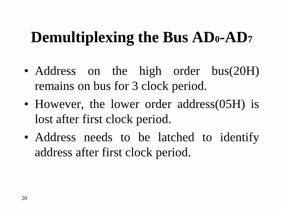
Demultiplexing the Bus AD0-AD7
• Address on the high order bus(20H)
remains on bus for 3 clock period.
• However, the lower order address(05H) is
lost after first clock period.
• Address needs to be latched to identify
address after first clock period.
20
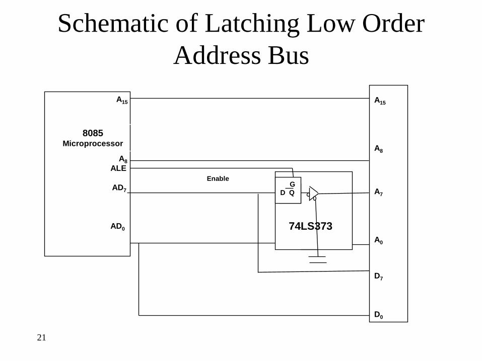
Schematic of Latching Low Order
Address Bus
21
8085 Microprocessor
A8
ALE
AD7
AD0
A15 A15
A8
A7
A0
D7
D0
Enable
74LS373
G
D Q
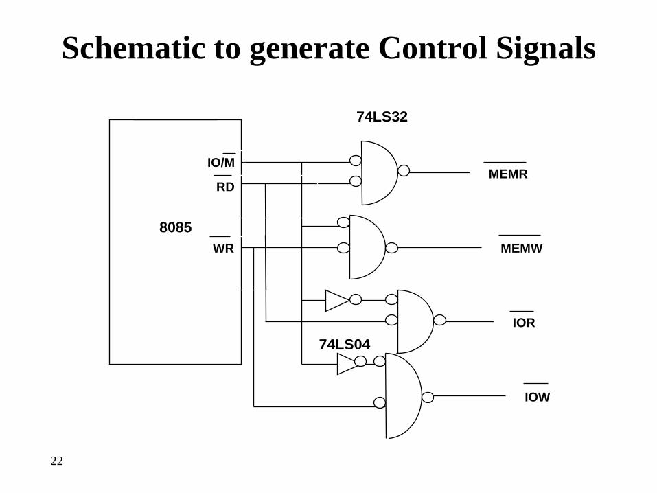
Schematic to generate Control Signals
22
8085
IO/M
RD
WR
MEMR
MEMW
IOR
IOW
74LS32
74LS04
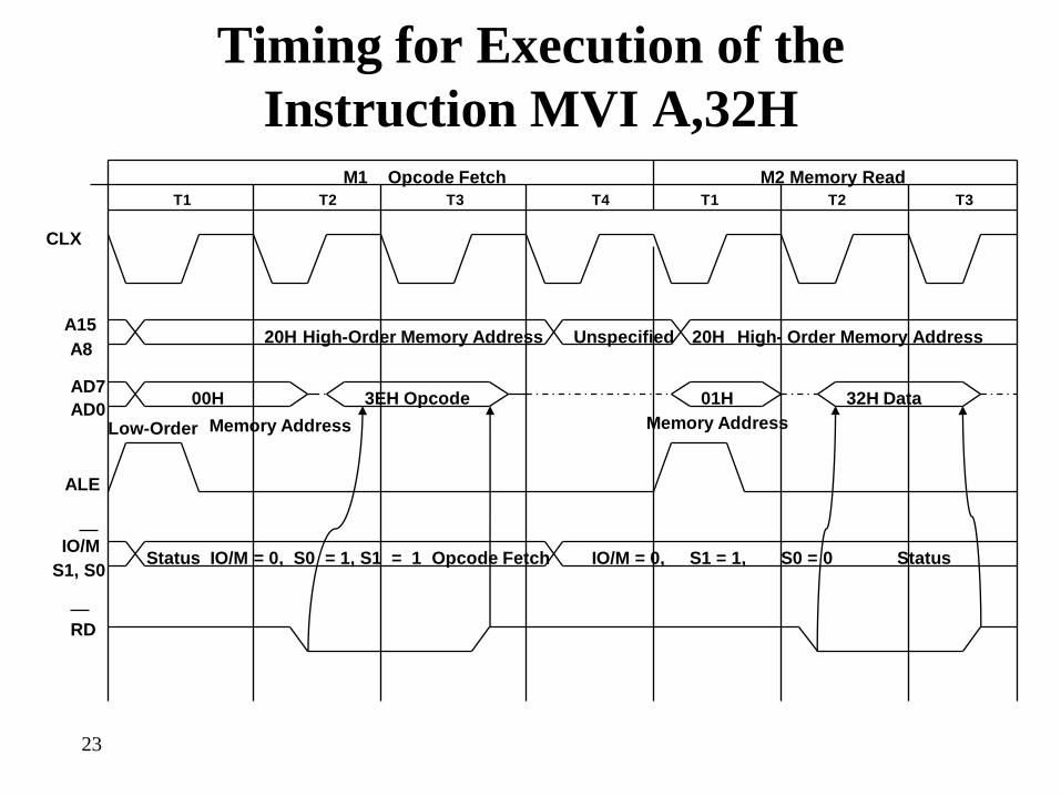
Timing for Execution of the
Instruction MVI A,32H
23
T1 T2 T3 T4
CLX
M1 Opcode Fetch
A15
A8
AD7
AD0
ALE
IO/M
RD
20H High-Order Memory Address Unspecified
Low-Order
00H 3EH Opcode
Memory Address
Status IO/M = 0, S0 = 1, S1 = 1 Opcode FetchS1, S0
M2 Memory Read
T1 T2 T3
20H High- Order Memory Address
01H 32H Data
Memory Address
IO/M = 0, S1 = 1, S0 = 0 Status