Embed Size (px)
Citation preview
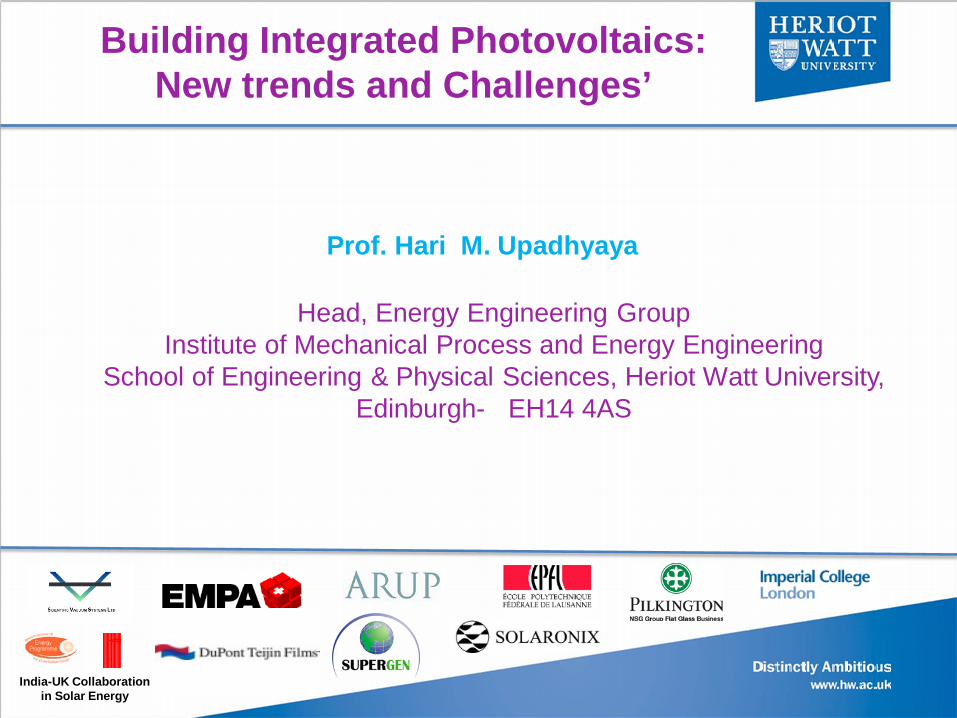
Building Integrated Photovoltaics: New trends and Challenges’
Prof. Hari M. Upadhyaya
Head, Energy Engineering Group Institute of Mechanical Process and Energy Engineering
School of Engineering & Physical Sciences, Heriot Watt University, Edinburgh- EH14 4AS
India-UK Collaboration in Solar Energy
Contents
1. Introduction: Global PV and BIPV scenario
2.PV Technologies
3.New Developments 4. Future Trends 5. Summary and Conclusion
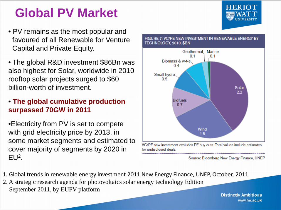
Global PV Market • PV remains as the most popular and favoured of all Renewable for Venture Capital and Private Equity.
• The global R&D investment $86Bn was also highest for Solar, worldwide in 2010 rooftop solar projects surged to $60 billion-worth of investment.
• The global cumulative production surpassed 70GW in 2011
•Electricity from PV is set to compete with grid electricity price by 2013, in some market segments and estimated to cover majority of segments by 2020 in EU2.
1. Global trends in renewable energy investment 2011 New Energy Finance, UNEP, October, 2011 2. A strategic research agenda for photovoltaics solar energy technology Edition September 2011, by EUPV platform
The built environment, although representing almost half of all EU carbon emissions, presents the ideal least impact environment, to both generate renewable energy and save energy… [HM government, Definition of zero carbon homes and non-domestic building, consultation Dec 2008]
Building Integrated Photovoltaics
• This glazing market is some 6.6bn m2 per year globally worth €51bn annually when processed
(Float glass for building 5.4 Billion m2 + 80 Million m2 for PV ) • BIPV market was1201MWp in 2011, is expected to grow annually over
the next couple of years by 56% p.a. to 11GWp by 2015 (BCC Research).
• Combining with façade glazing and all BIPV applications together this is around a £100bn, which compares very well with the current terrestrial solar PV market.
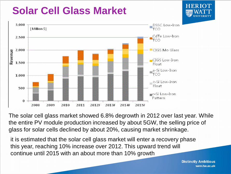
The solar cell glass market showed 6.8% degrowth in 2012 over last year. While the entire PV module production increased by about 5GW, the selling price of glass for solar cells declined by about 20%, causing market shrinkage.
it is estimated that the solar cell glass market will enter a recovery phase this year, reaching 10% increase over 2012. This upward trend will continue until 2015 with an about more than 10% growth
Solar Cell Glass Market
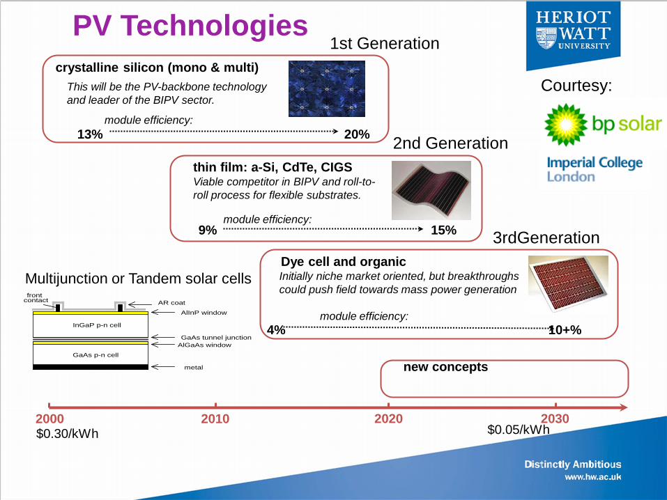
PV Technologies
2000 2030 2010 2020
crystalline silicon (mono & multi)
Dye cell and organic
thin film: a-Si, CdTe, CIGS
new concepts
This will be the PV-backbone technology and leader of the BIPV sector.
module efficiency:
Viable competitor in BIPV and roll-to-roll process for flexible substrates.
Initially niche market oriented, but breakthroughs could push field towards mass power generation module efficiency:
$0.30/kWh $0.05/kWh
13% 20%
9% 15% module efficiency:
4% 10+%
Courtesy:
metal
AlGaAs windowGaAs tunnel junction
AlInP window
AR coat
InGaP p-n cell
GaAs p-n cell
front contact
1st Generation
3rdGeneration
2nd Generation
Multijunction or Tandem solar cells
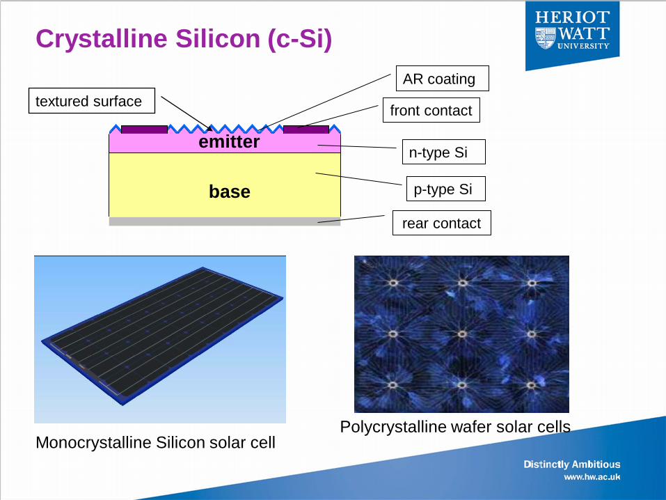
Crystalline Silicon (c-Si)
emitter
base rear contact
n-type Si
front contact textured surface AR coating
p-type Si
Monocrystalline Silicon solar cell Polycrystalline wafer solar cells
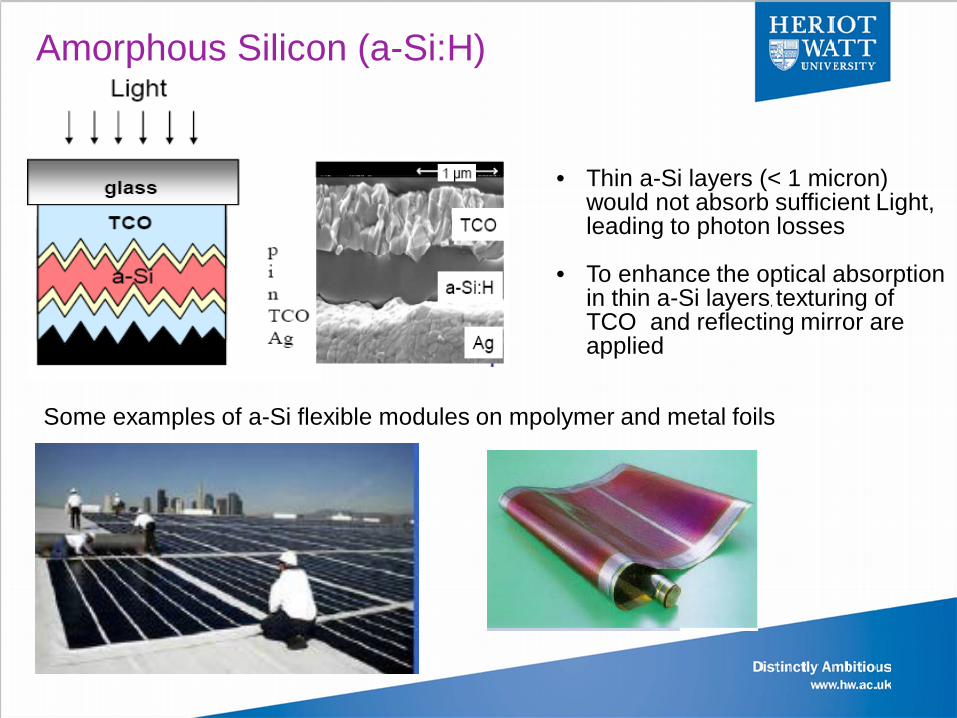
• Thin a-Si layers (< 1 micron) would not absorb sufficient Light, leading to photon losses
• To enhance the optical absorption in thin a-Si layers, texturing of TCO and reflecting mirror are applied
Amorphous Silicon (a-Si:H)
Some examples of a-Si flexible modules on mpolymer and metal foils
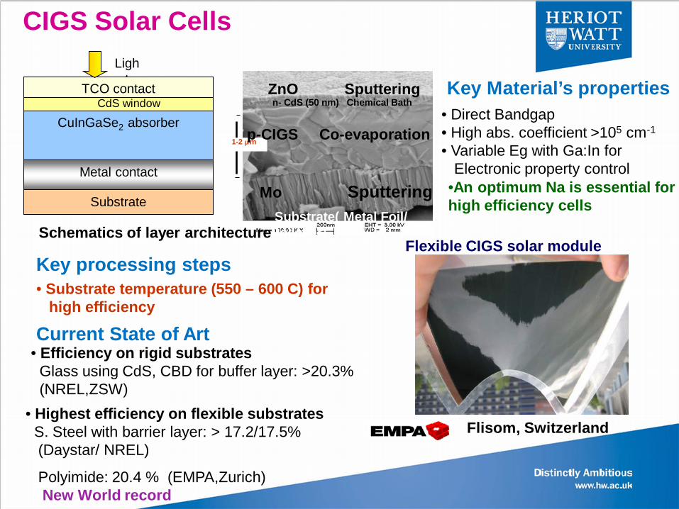
CIGS Solar Cells Ligh
t TCO contact
Substrate
Metal contact
CuInGaSe2 absorber CdS window
Sputtering
Mo Sputtering
1-2 µm
ZnO
Substrate( Metal Foil/ Polymer)
n- CdS (50 nm) Chemical Bath
p-CIGS Co-evaporation
Schematics of layer architecture
• Highest efficiency on flexible substrates S. Steel with barrier layer: > 17.2/17.5% (Daystar/ NREL)
Polyimide: 20.4 % (EMPA,Zurich) New World record
• Efficiency on rigid substrates Glass using CdS, CBD for buffer layer: >20.3% (NREL,ZSW)
Current State of Art
• Direct Bandgap • High abs. coefficient >105 cm-1 • Variable Eg with Ga:In for Electronic property control
• Substrate temperature (550 – 600 C) for high efficiency
Key Material’s properties
Key processing steps
Flisom, Switzerland
Flexible CIGS solar module
•An optimum Na is essential for high efficiency cells
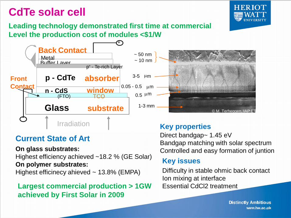
CdTe solar cell
3-5 µ m
Irradiation
- Glass
(FTO)
p - CdTe
~ 10 nm ~ 50 nm
Buffer Layer Metal
Back Contact
p + - Te-rich Layer
0.5
1-3 mm
n - CdS
+
absorber window
Front Contact
substrate © M. Terheggen, IAP ETHZ
0.05 - 0.5 µm µm TCO
Current State of Art On glass substrates: Highest efficiency achieved ~18.2 % (GE Solar) On polymer substrates: Highest efficinecy ahieved ~ 13.8% (EMPA)
Key properties Direct bandgap~ 1.45 eV Bandgap matching with solar spectrum Controlled and easy formation of juntion Key issues Difficulty in stable ohmic back contact Ion mixing at interface Essential CdCl2 treatment Largest commercial production > 1GW
achieved by First Solar in 2009
Leading technology demonstrated first time at commercial Level the production cost of modules <$1/W
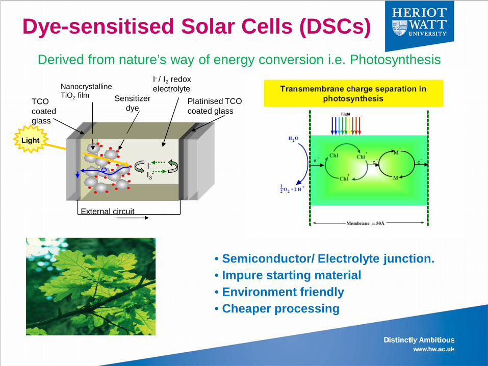
Platinised TCO coated glass
I- / I2 redox electrolyte
Light
External circuit
TCO coated glass
Nanocrystalline TiO2 film
I3- I-
Sensitizer dye
Derived from nature’s way of energy conversion i.e. Photosynthesis
Dye-sensitised Solar Cells (DSCs)
• Semiconductor/ Electrolyte junction. • Impure starting material • Environment friendly • Cheaper processing
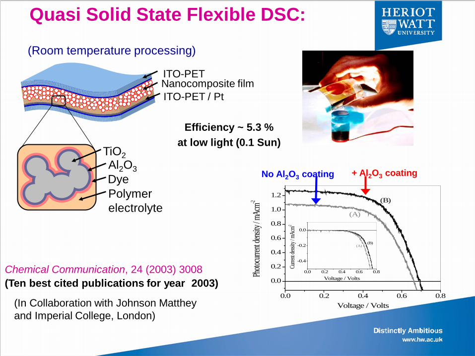
Quasi Solid State Flexible DSC:
ITO-PET Nanocomposite film ITO-PET / Pt
Dye
TiO2 Al2O3
Polymer electrolyte
Efficiency ~ 5.3 % at low light (0.1 Sun)
(Room temperature processing)
(Ten best cited publications for year 2003) Chemical Communication, 24 (2003) 3008
(In Collaboration with Johnson Matthey and Imperial College, London)
0.0 0.2 0.4 0.6 0.8
0.0
0.2
0.4
0.6
0.8
1.0
1.2
0.0 0.2 0.4 0.6 0.8
-0.4
-0.2
0.0
(B)(A)
Curre
nt den
sity / m
Acm-2
Voltage / Volts
(B)
(A)
Photo
curren
t dens
ity / m
Acm-2
Voltage / Volts
+ Al2O3 coating No Al2O3 coating
13
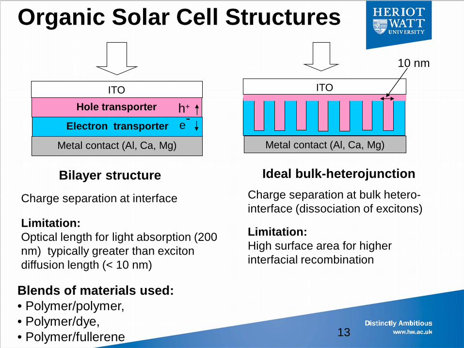
Organic Solar Cell Structures
ITO
Electron transporter
Metal contact (Al, Ca, Mg)
Hole transporter
e- h+
Charge separation at interface Limitation: Optical length for light absorption (200 nm) typically greater than exciton diffusion length (< 10 nm)
ITO
Metal contact (Al, Ca, Mg)
10 nm
Charge separation at bulk hetero- interface (dissociation of excitons) Limitation: High surface area for higher interfacial recombination
Bilayer structure Ideal bulk-heterojunction
Blends of materials used: • Polymer/polymer, • Polymer/dye, • Polymer/fullerene
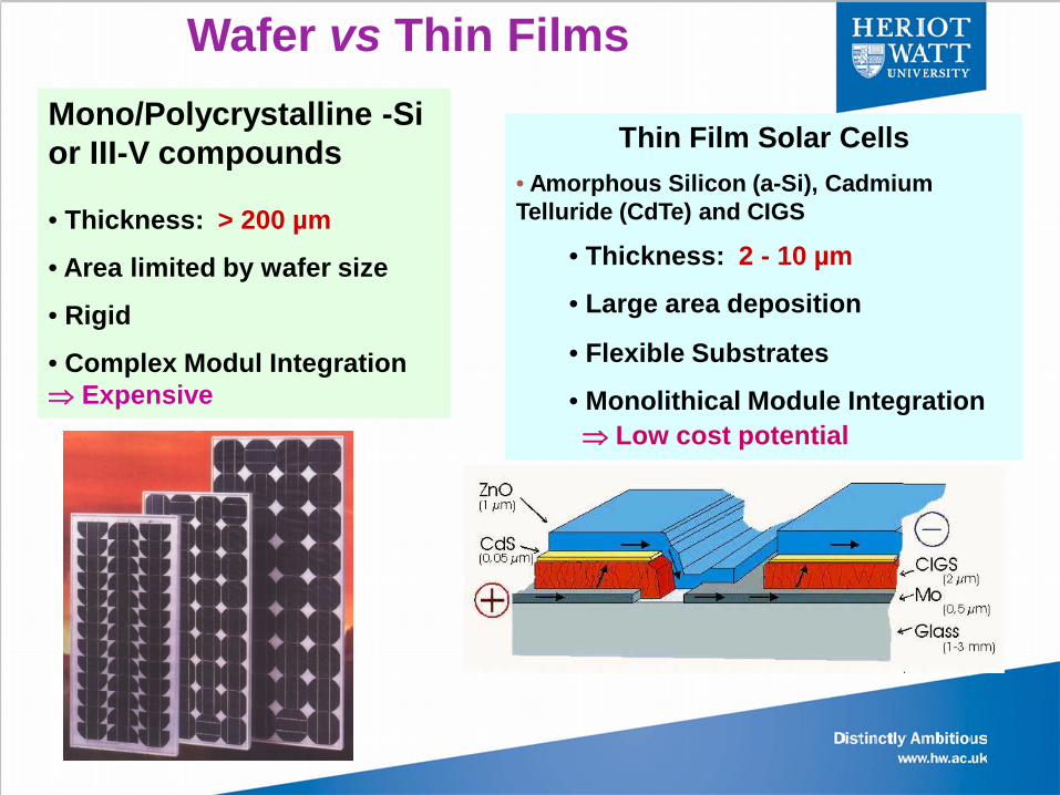
Wafer vs Thin Films Mono/Polycrystalline -Si or III-V compounds • Thickness: > 200 µm
• Area limited by wafer size
• Rigid
• Complex Modul Integration ⇒ Expensive
Thin Film Solar Cells
• Amorphous Silicon (a-Si), Cadmium Telluride (CdTe) and CIGS
• Thickness: 2 - 10 µm
• Large area deposition
• Flexible Substrates
• Monolithical Module Integration ⇒ Low cost potential
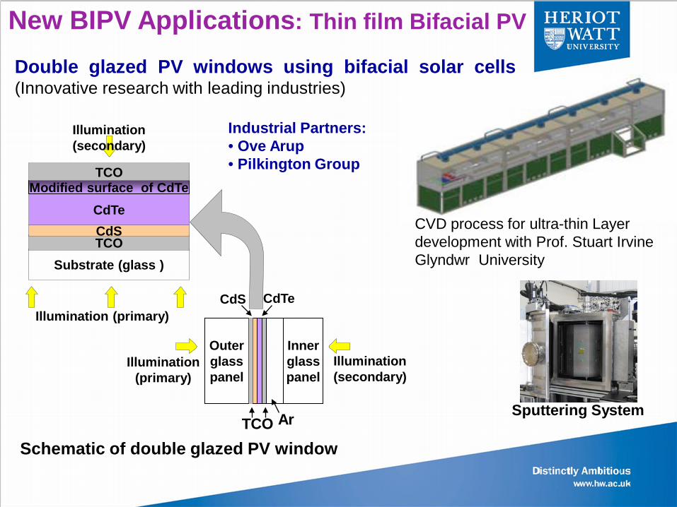
Industrial Partners: • Ove Arup • Pilkington Group
TCO
CdTe CdS
Ar
Outer glass panel
Inner glass panel
Illumination (secondary)
Illumination (primary)
Double glazed PV windows using bifacial solar cells (Innovative research with leading industries)
Schematic of double glazed PV window
Substrate (glass ) TCO CdS CdTe
Modified surface of CdTe TCO
Illumination (primary)
Illumination (secondary)
Sputtering System
CVD process for ultra-thin Layer development with Prof. Stuart Irvine Glyndwr University
New BIPV Applications: Thin film Bifacial PV
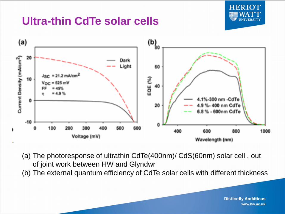
Ultra-thin CdTe solar cells
(a) The photoresponse of ultrathin CdTe(400nm)/ CdS(60nm) solar cell , out of joint work between HW and Glyndwr
(b) The external quantum efficiency of CdTe solar cells with different thickness
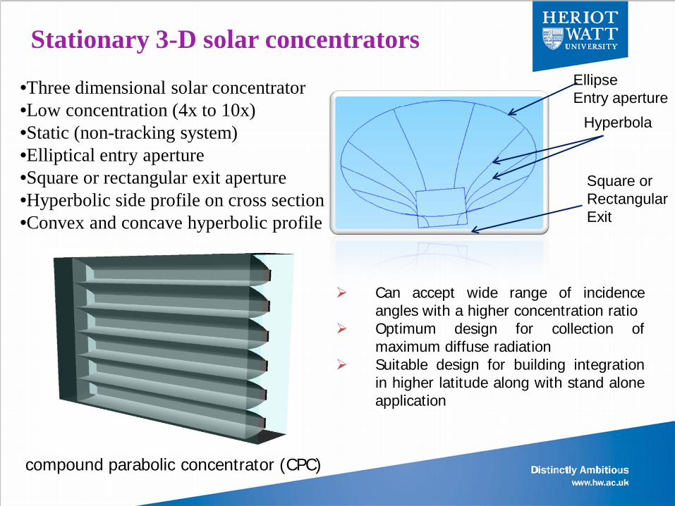
Stationary 3-D solar concentrators •Three dimensional solar concentrator •Low concentration (4x to 10x) •Static (non-tracking system) •Elliptical entry aperture •Square or rectangular exit aperture •Hyperbolic side profile on cross section •Convex and concave hyperbolic profile
Ellipse Entry aperture
Hyperbola
Square or Rectangular Exit
compound parabolic concentrator (CPC)
Can accept wide range of incidence angles with a higher concentration ratio
Optimum design for collection of maximum diffuse radiation
Suitable design for building integration in higher latitude along with stand alone application
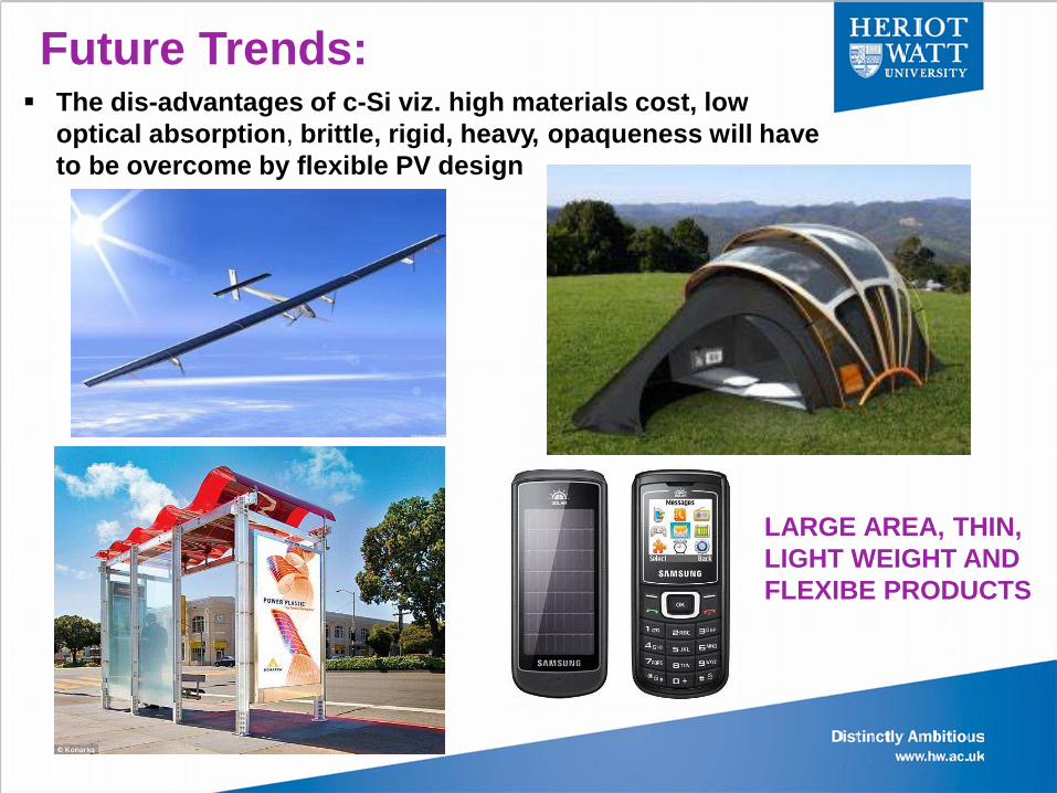
Future Trends: The dis-advantages of c-Si viz. high materials cost, low
optical absorption, brittle, rigid, heavy, opaqueness will have to be overcome by flexible PV design
LARGE AREA, THIN, LIGHT WEIGHT AND FLEXIBE PRODUCTS
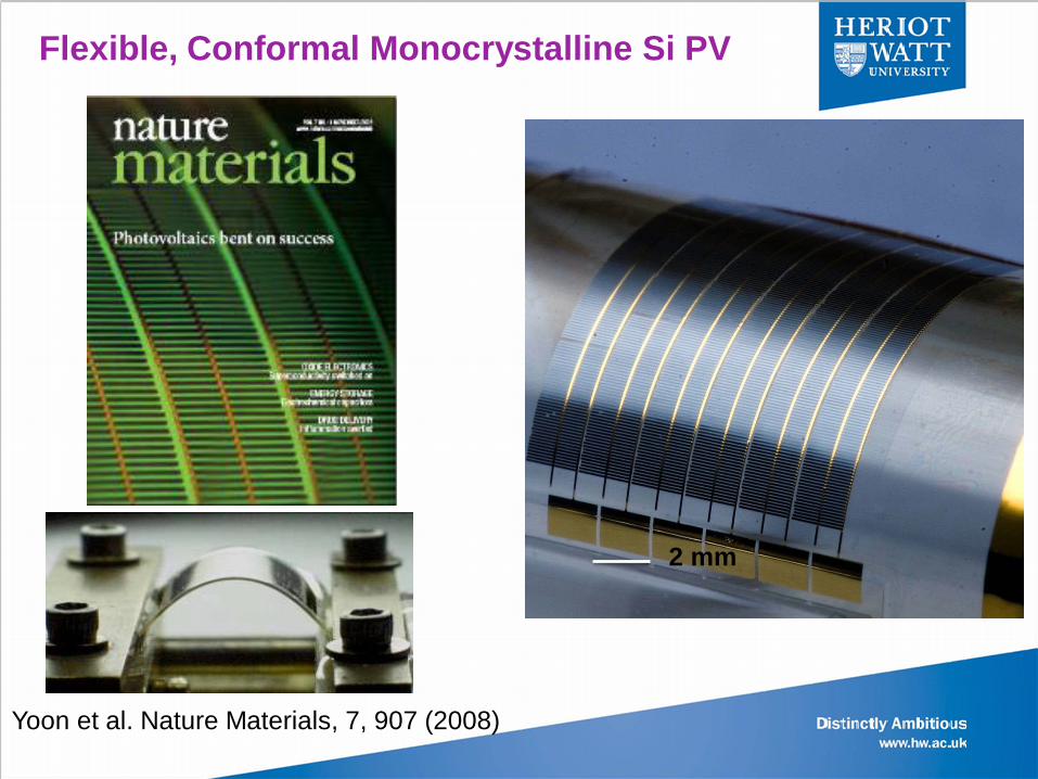
Yoon et al. Nature Materials, 7, 907 (2008)
2 mm
Flexible, Conformal Monocrystalline Si PV
The BIPV sector which is backed by an established glazing industry is set to grow over 50% rate in the future.
The dis-advantages of c-Si viz. high materials cost, low optical absorption, brittle, rigid, heavy, opaqueness will have to be overcome by flexible thin-film bifacial PV.
Thin-film modules allow greater freedom to select size and colour than c-Si module, e.g. module efficiency decreases as the temperature increases for mono and poly silicon cells but not for amorphous silicon cells.
The challenge lies with achieving the colour neutral glazing which is limited by a coloured tinge of the glass.
New concentrator PV designs combined with thermal integration will make it a viable industry in the future in a large number of countries.
Summary and Conclusions
Acknowledgements:
M. Graetzel, EPFL, Switzerland
Ayodhya Tiwari, ETH Zurich, Switzerland
Marc Kaelin, ETH Zurich, Switzerland
Prof. Tapas K. Mallick, Exeter University
Prof. Stuart Irvine, Glyndwr Univeristy

Thanks for your attention!