Embed Size (px)
Citation preview
Bulk Fermi surface coexistence with Dirac surface state in Bi2Se3: A comparison of photoemissionand Shubnikov–de Haas measurements
James G. Analytis,1,2 Jiun-Haw Chu,1,2 Yulin Chen,1,2 Felipe Corredor,1,2 Ross D. McDonald,3 Z. X. Shen,1,2 andIan R. Fisher1,2
1Stanford Institute for Materials and Energy Sciences, SLAC National Accelerator Laboratory, 2575 Sand Hill Road,Menlo Park, California 94025, USA
2Geballe Laboratory for Advanced Materials and Department of Applied Physics, Stanford University, Stanford, California 94305, USA3Los Alamos National Laboratory, Los Alamos, New Mexico 87545, USA
�Received 2 February 2010; published 5 May 2010�
Shubnikov-de Haas �SdH� oscillations and angle-resolved photoemission spectroscopy �ARPES� are used toprobe the Fermi surface of single crystals of Bi2Se3. We find that SdH and ARPES probes quantitatively agreeon measurements of the effective mass and bulk band dispersion. In high carrier density samples, the twoprobes also agree in the exact position of the Fermi level EF, but for lower carrier density samples discrepan-cies emerge in the position of EF. In particular, SdH reveals a bulk three-dimensional Fermi surface forsamples with carrier densities as low as 1017 cm−3. We suggest a simple mechanism to explain these differ-ences and discuss consequences for existing and future transport studies of topological insulators.
DOI: 10.1103/PhysRevB.81.205407 PACS number�s�: 72.20.My, 03.65.Vf, 71.70.Di, 73.25.�i
Recently, a new state of matter, known as a topologicalinsulator, has been predicted to exist in a number of materi-als: Bi1−xSbx, Bi2Se3, Bi2Te3, and Sb2Te3.1,2 This state ofmatter is characterized by a full band gap in the bulk of thematerial, but with a gapless, dissipationless surface state. Thesurface state is comprised of counter-propagating spin states,which create a dispersion of a single, massless Dirac conethat is protected by time-reversal symmetry. The experimen-tal realization of this state could mean significant advances inspintronic devices, quantum computation, and much morebesides.
As a result there has been great excitement in the last yearafter the discoveries of various angle-resolved photoemissionspectroscopy �ARPES� experiments3–5 and more recentlyfrom scanning-tunneling measurements6–8 that such a stateappears to exist in nature. Amidst this flurry of recent results,it is easy to forget that these same materials have been thesubject of careful and thorough research for much of the 20thcentury. However, common to all the unambiguous measure-ments of the Dirac cone is the use of surface-sensitiveprobes. Only recently have transport measurements emergedspecifically investigating the surface state �Refs. 9–11�, all ofwhich note the dominance of the bulk conductivity. It is thusof great interest to perform a coordinated study of these ma-terials using both bulk transport experiments and surfacesensitive ARPES experiments. Here we report results ofthese investigations. The transport experiments reveal quan-tum oscillations that indicate a bulk Fermi surface volumethat monotonically changes with carrier density. For carrierdensities in the range �1019 cm−3, the transport extractedband structure is in quantitative agreement with the bulkband structure determined by ARPES which also observesthe Dirac dispersion of the surface state. The quantitativeagreement between ARPES and SdH provides additionalsupport for the existence of novel band structure in thesematerials. For lower carrier density samples down to1017 cm−3 we observe SdH oscillations which unambigu-ously pin the Fermi level in the bulk conduction band, with a
high level of consistency across all samples measured fromthe same batch. While ARPES places EF near the SdH levelfor some samples, there are others from the same batchwhose EF is found to reside into the bulk gap. We discusspossible explanations for these discrepancies and the impli-cations for transport studies of surface Dirac fermions insamples near a metal-insulator transition.
The material Bi2Se3 can be grown without the introduc-tion of foreign dopants as either n or p type12,13 though ismore commonly found as the former because the dominantdefects tend to be Se vacancies. Quantum oscillatory phe-nomena, which provides evidence of bulk metallic behaviorhas been reported by Köhler12 on low carrier density samplesand more recently by Kulbachinskii14 on high carrier densitysamples. Below a carrier density of 7�1018 cm−3, the bandstructure is well approximated by a single parabolic band,making the interpretation of transport measurementstransparent.14 Two n-type samples with carrier densities dif-fering by 2 orders of magnitude are shown in Fig. 1. For thelow carrier density samples an upturn in the resistivity isseen, which levels off at sufficiently low temperature. Thisbehavior has been attributed to the presence of an impurityband whose thermally activated conductivity is comparableto the band conductivity until carriers freeze out at around 30K.13,14 This behavior is not apparent in the higher carrierdensity materials, where the band conductivity always domi-nates. Furthermore, the mobility increases as the carrier den-sity decreases, consistent with previous measurements.14 Thecarrier densities of our highest mobility samples are aroundan order of magnitude smaller than those of reported topo-logical insulators including Sn-doped Bi2Te3�ne�1.7�1018 cm−3� �Ref. 4� or Ca-doped Bi2Se3�ne�5�1018 cm−3� �Ref. 5� and as a result may be better candi-dates in which to observe the transport properties dominatedby the topological surface state.
Single crystals of Bi2Se3 have been grown by slow cool-ing a binary melt. Elemental Bi and Se were mixed in alu-mina crucibles in a molar ratio of 35:65 for batch S1 �ne
PHYSICAL REVIEW B 81, 205407 �2010�
1098-0121/2010/81�20�/205407�5� ©2010 The American Physical Society205407-1
=5�1017�, 34:66 for batch S2 �ne=3�1017�, 34:66 forbatch S3 �ne=2.3�1017�, and 40:60 for batch S4 �ne=2.3�1019�. The mixtures were sealed in quartz ampules andraised to 750 °C and cooled slowly to 550 °C, then an-nealed for an extended period. Crystals can be cleaved veryeasily perpendicular to the �0 0 1� axis. Measurements of theresistivity and Hall effect were measured in a 14 T PPMSusing a standard four-probe contact configuration and Hallmeasurements were performed using a six-probe configura-tion. For the latter, only data which were linear in the low-field limit were used to avoid mixing with longitudinal com-ponents. In addition to this precaution, signal from positiveand negative field sweeps was subtracted to extract the odd�Hall� components of the signal, after which the carrier den-sity is extracted in the usual way. ARPES measurementswere performed at beam line 10.0.1 of the Advanced LightSource �ALS� at Lawrence Berkeley National Laboratory.Measurement pressure was kept �3�10−11 Torr, and datawere recorded by Scienta R4000 analyzers at 15 K sampletemperature. The total convolved energy and angle resolu-tions were 16 meV and 0.2° �i.e., �0.007 �Å−1� or�0.012�1 Å−1� for photoelectrons generated by 48 eV pho-tons�, at which energy the cross-section for both surface stateand bulk bands is strong.
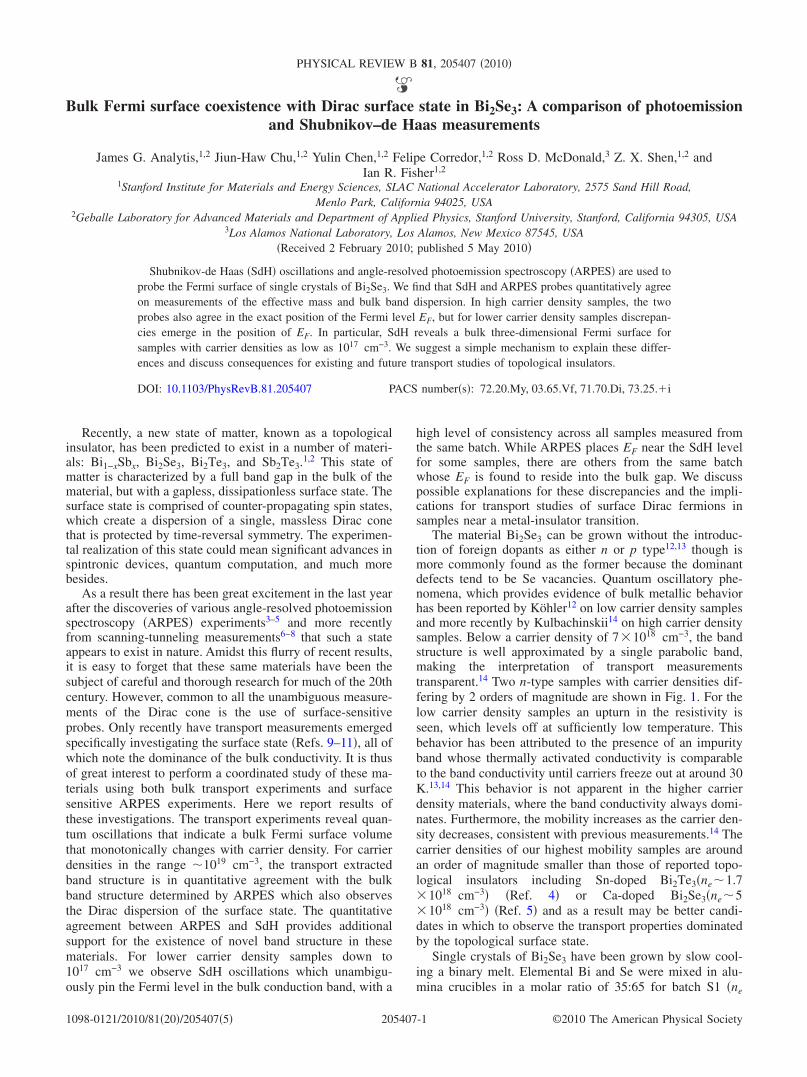
In Fig. 2 we show complimentary ARPES and SdH dataon samples from the same batch with carrier density deter-mined by the Hall effect of ne=2.3�1019 cm−3. The SdHreveals an anisotropic pocket of frequency 155 T, corre-sponding to a Fermi energy of around 155 meV above thebottom of the conduction band �the band structure is notparabolic at this filling and so we assume similar band-structure parameters as Köhler12 characterizing similar car-rier density samples of Bi2Se3�. ARPES results on samplesfrom the same batch show the Fermi level 150 meV abovethe bottom of the conduction band in good quantitativeagreement. Similarly, the effective mass �see below� ex-
tracted from SdH is in good quantitative agreement with thatmeasured by ARPES.
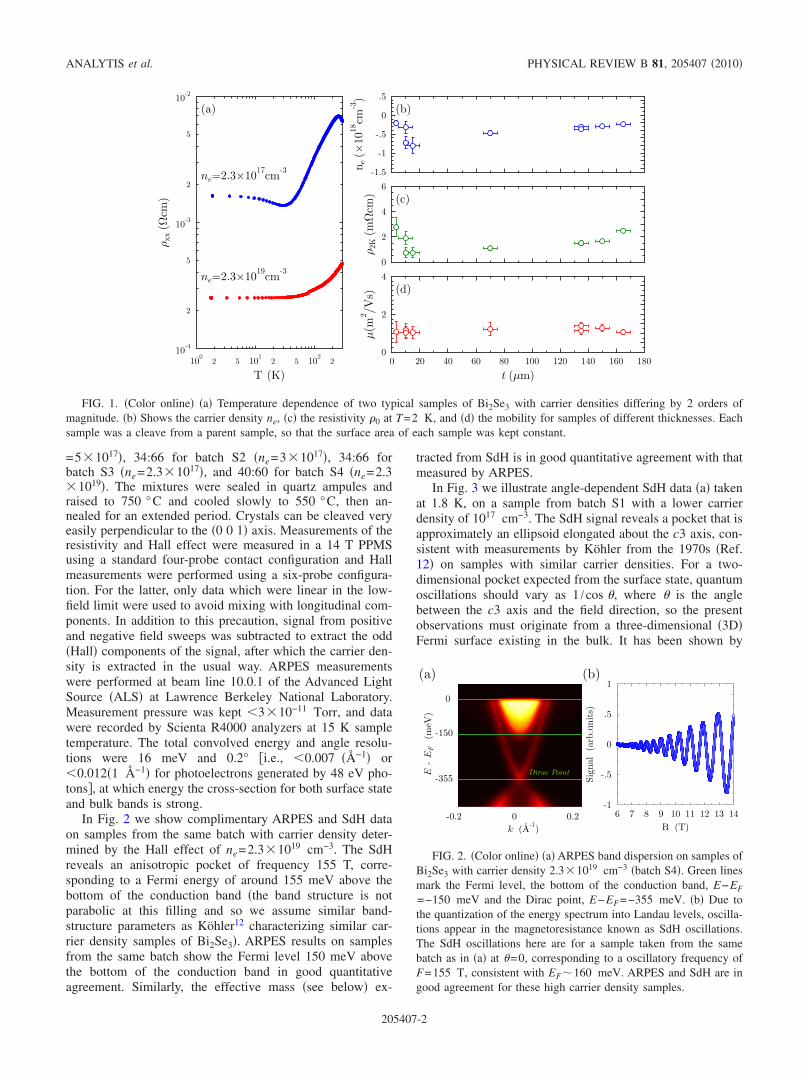
In Fig. 3 we illustrate angle-dependent SdH data �a� takenat 1.8 K, on a sample from batch S1 with a lower carrierdensity of 1017 cm−3. The SdH signal reveals a pocket that isapproximately an ellipsoid elongated about the c3 axis, con-sistent with measurements by Köhler from the 1970s �Ref.12� on samples with similar carrier densities. For a two-dimensional pocket expected from the surface state, quantumoscillations should vary as 1 /cos �, where � is the anglebetween the c3 axis and the field direction, so the presentobservations must originate from a three-dimensional �3D�Fermi surface existing in the bulk. It has been shown by
FIG. 1. �Color online� �a� Temperature dependence of two typical samples of Bi2Se3 with carrier densities differing by 2 orders ofmagnitude. �b� Shows the carrier density ne, �c� the resistivity �0 at T=2 K, and �d� the mobility for samples of different thicknesses. Eachsample was a cleave from a parent sample, so that the surface area of each sample was kept constant.
FIG. 2. �Color online� �a� ARPES band dispersion on samples ofBi2Se3 with carrier density 2.3�1019 cm−3 �batch S4�. Green linesmark the Fermi level, the bottom of the conduction band, E−EF
=−150 meV and the Dirac point, E−EF=−355 meV. �b� Due tothe quantization of the energy spectrum into Landau levels, oscilla-tions appear in the magnetoresistance known as SdH oscillations.The SdH oscillations here are for a sample taken from the samebatch as in �a� at �=0, corresponding to a oscillatory frequency ofF=155 T, consistent with EF�160 meV. ARPES and SdH are ingood agreement for these high carrier density samples.
ANALYTIS et al. PHYSICAL REVIEW B 81, 205407 �2010�
205407-2
Köhler12 and more recently by Kulbachinskii et al.14 that theconduction-band structure for these low carrier densities isapproximately parabolic, and so the band filling can be esti-
mated by EF=�2Ak
2�m� , where Ak is the area of the Fermi surfacein Fourier space. The Shubnikov-de Haas frequency is�18 T corresponding to a Fermi energy of 17 meV abovethe bottom of the conduction band.
In Fig. 3�b� we show the derivative of the longitudinalmagnetoresistance of a sample from batch S3 and a fit of theentire data set using the usual Lifshitz-Kosevich formalism,15
to extract the effective mass and Dingle temperature TD, withfit shown in Fig. 3�c�. Fitting the entire data set, which isoften more accurate than tracing the amplitude of the Fouriertransform, our fit yields m�=0.15me and TD=3.5 K, for thisfrequency �F=14 T�. Similar data for samples from batchS4 give m�=0.125me, TD=4 K, and F=155 T. The meanfree path is calculated using the orbitally averaged velocityand scattering time extracted from TD yields lS3�60 nm andlS4�220 nm. These data are wholly consistent with the verycomplete SdH studies of Köhler et al.12,13 and more recentlyby Kulbachinskii et al.14 In addition, the data were repro-duced with high consistency on a number of samples fromthe same batch, and even on samples from different batcheswith similar growth parameters.
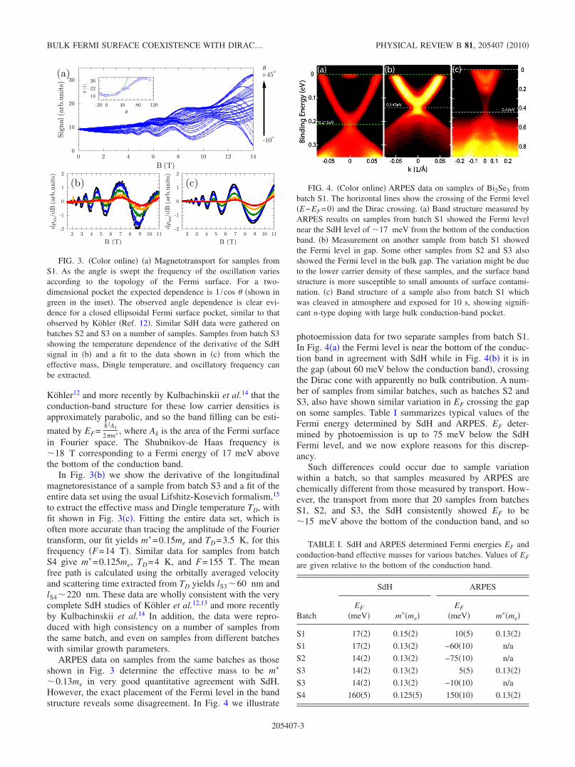
ARPES data on samples from the same batches as thoseshown in Fig. 3 determine the effective mass to be m�
�0.13me in very good quantitative agreement with SdH.However, the exact placement of the Fermi level in the bandstructure reveals some disagreement. In Fig. 4 we illustrate
photoemission data for two separate samples from batch S1.In Fig. 4�a� the Fermi level is near the bottom of the conduc-tion band in agreement with SdH while in Fig. 4�b� it is inthe gap �about 60 meV below the conduction band�, crossingthe Dirac cone with apparently no bulk contribution. A num-ber of samples from similar batches, such as batches S2 andS3, also have shown similar variation in EF crossing the gapon some samples. Table I summarizes typical values of theFermi energy determined by SdH and ARPES. EF deter-mined by photoemission is up to 75 meV below the SdHFermi level, and we now explore reasons for this discrep-ancy.
Such differences could occur due to sample variationwithin a batch, so that samples measured by ARPES arechemically different from those measured by transport. How-ever, the transport from more that 20 samples from batchesS1, S2, and S3, the SdH consistently showed EF to be�15 meV above the bottom of the conduction band, and so
FIG. 3. �Color online� �a� Magnetotransport for samples fromS1. As the angle is swept the frequency of the oscillation variesaccording to the topology of the Fermi surface. For a two-dimensional pocket the expected dependence is 1 /cos � �shown ingreen in the inset�. The observed angle dependence is clear evi-dence for a closed ellipsoidal Fermi surface pocket, similar to thatobserved by Köhler �Ref. 12�. Similar SdH data were gathered onbatches S2 and S3 on a number of samples. Samples from batch S3showing the temperature dependence of the derivative of the SdHsignal in �b� and a fit to the data shown in �c� from which theeffective mass, Dingle temperature, and oscillatory frequency canbe extracted.
FIG. 4. �Color online� ARPES data on samples of Bi2Se3 frombatch S1. The horizontal lines show the crossing of the Fermi level�E−EF=0� and the Dirac crossing. �a� Band structure measured byARPES results on samples from batch S1 showed the Fermi levelnear the SdH level of �17 meV from the bottom of the conductionband. �b� Measurement on another sample from batch S1 showedthe Fermi level in gap. Some other samples from S2 and S3 alsoshowed the Fermi level in the bulk gap. The variation might be dueto the lower carrier density of these samples, and the surface bandstructure is more susceptible to small amounts of surface contami-nation. �c� Band structure of a sample also from batch S1 whichwas cleaved in atmosphere and exposed for 10 s, showing signifi-cant n-type doping with large bulk conduction-band pocket.
TABLE I. SdH and ARPES determined Fermi energies EF andconduction-band effective masses for various batches. Values of EF
are given relative to the bottom of the conduction band.
Batch
SdH ARPES
EF
�meV� m��me�EF
�meV� m��me�
S1 17�2� 0.15�2� 10�5� 0.13�2�S1 17�2� 0.13�2� −60�10� n/a
S2 14�2� 0.13�2� −75�10� n/a
S3 14�2� 0.13�2� 5�5� 0.13�2�S3 14�2� 0.13�2� −10�10� n/a
S4 160�5� 0.125�5� 150�10� 0.13�2�
BULK FERMI SURFACE COEXISTENCE WITH DIRAC… PHYSICAL REVIEW B 81, 205407 �2010�
205407-3
sample dependence seems unlikely. Another reason for thediscrepancy may be that atmospheric exposure of transportsamples has contaminated them with an n-type dopant caus-ing them to appear bulk n type. Figure 4�c� illustrates pho-toemission data for a sample cleaved in air. The Dirac coneof the surface state remains robust and the bulk conductionband appears partially occupied. Such doping may lead to a3D Fermi surface pocket appearing in SdH oscillations if thecontamination is deep enough and allows for sufficientlylong mean free paths.
To investigate this possibility further we measure thethickness dependence of the transport by systematically thin-ning a single sample. Cleaving was achieved with tape, keep-ing the cross-sectional area of the resulting samples rela-tively constant and allowing direct comparison of data sets ofeach cleave. Though the samples are vulnerable to deforma-tions between cleaves, only data from mirrorlike flat samplesare presented. In most cases these samples still exhibitedquantum oscillatory phenomena, confirming the high qualityof the cleaved samples. Figures 1�b�–1�d� show a summaryof the low-temperature carrier density, resistivity, and mobil-ity as a function of thickness. Within our error bars, eachquantity seems to vary weakly down to 3 �m in thickness.Although the residual resistivity and carrier density varyslightly �possibly from disorder related to slight sample de-formation, despite the precautions mentioned above�, themobility remains almost constant as a function of thicknessat ��1 m2 /V s. In summary, the transport is insensitive tothe thickness, suggesting that the SdH oscillations are not aconsequence of atmospheric contamination, but originatefrom the intrinsic band conductivity of the bulk.
A final scenario for the discrepancy is that the band struc-ture is distorted near the surface due to space-charge accu-mulation. This is known to occur in many semiconductors,such as InSb or CdTe,16,17 whereby the bulk band structurebends as the surface is approached. Typically, such bendingoccurs over a surface depletion layer zd, which can be calcu-lated by solving the Poisson equation to yield zd
2
=0�V /ene,18 where is the dc dielectric permittivity �es-
timated from these samples as �113 �Ref. 19�� and �V is thedifference in energy between the surface and bulk states. Weestimate zd
S1�40 nm for the low carrier density samples andzd
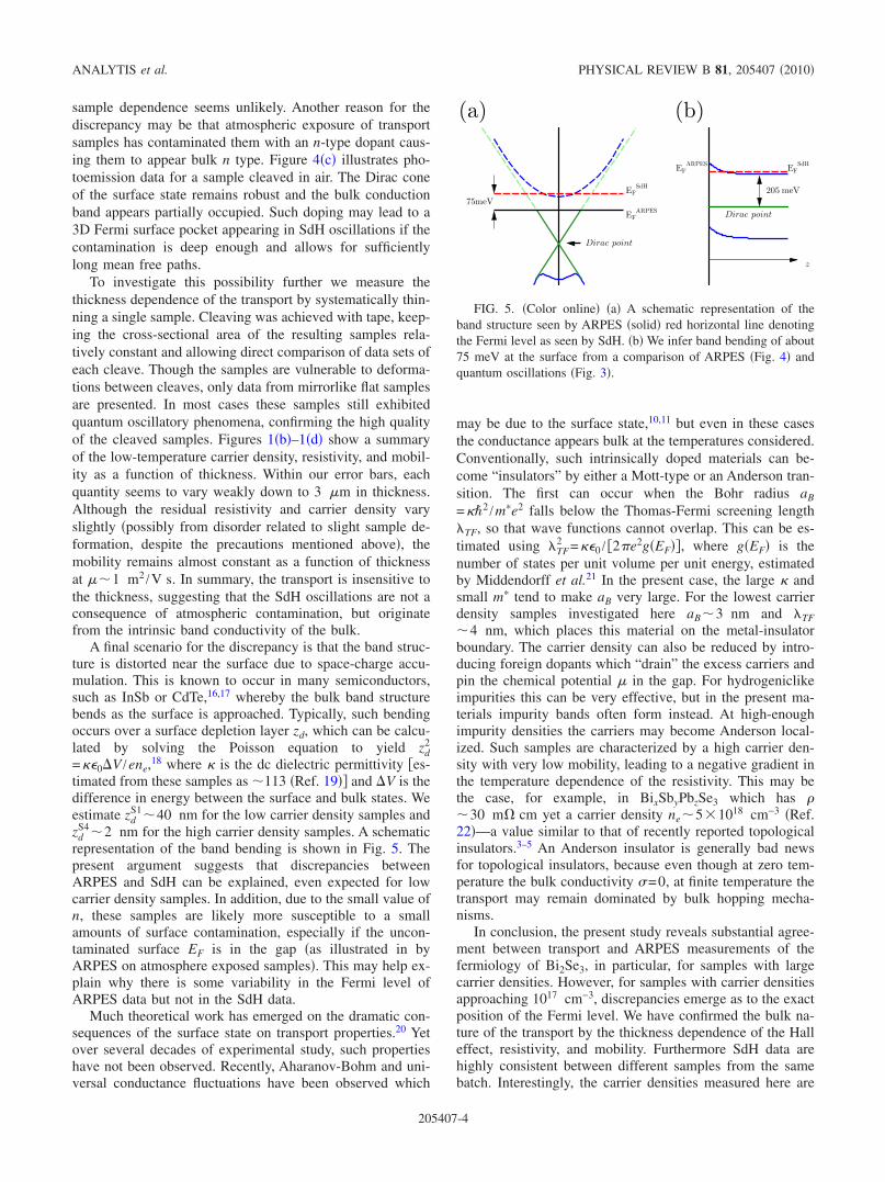
S4�2 nm for the high carrier density samples. A schematicrepresentation of the band bending is shown in Fig. 5. Thepresent argument suggests that discrepancies betweenARPES and SdH can be explained, even expected for lowcarrier density samples. In addition, due to the small value ofn, these samples are likely more susceptible to a smallamounts of surface contamination, especially if the uncon-taminated surface EF is in the gap �as illustrated in byARPES on atmosphere exposed samples�. This may help ex-plain why there is some variability in the Fermi level ofARPES data but not in the SdH data.
Much theoretical work has emerged on the dramatic con-sequences of the surface state on transport properties.20 Yetover several decades of experimental study, such propertieshave not been observed. Recently, Aharanov-Bohm and uni-versal conductance fluctuations have been observed which
may be due to the surface state,10,11 but even in these casesthe conductance appears bulk at the temperatures considered.Conventionally, such intrinsically doped materials can be-come “insulators” by either a Mott-type or an Anderson tran-sition. The first can occur when the Bohr radius aB
=�2 /m�e2 falls below the Thomas-Fermi screening length�TF, so that wave functions cannot overlap. This can be es-timated using �TF
2 =0 / �2�e2g�EF��, where g�EF� is thenumber of states per unit volume per unit energy, estimatedby Middendorff et al.21 In the present case, the large andsmall m� tend to make aB very large. For the lowest carrierdensity samples investigated here aB�3 nm and �TF�4 nm, which places this material on the metal-insulatorboundary. The carrier density can also be reduced by intro-ducing foreign dopants which “drain” the excess carriers andpin the chemical potential � in the gap. For hydrogeniclikeimpurities this can be very effective, but in the present ma-terials impurity bands often form instead. At high-enoughimpurity densities the carriers may become Anderson local-ized. Such samples are characterized by a high carrier den-sity with very low mobility, leading to a negative gradient inthe temperature dependence of the resistivity. This may bethe case, for example, in BixSbyPbzSe3 which has ��30 m cm yet a carrier density ne�5�1018 cm−3 �Ref.22�—a value similar to that of recently reported topologicalinsulators.3–5 An Anderson insulator is generally bad newsfor topological insulators, because even though at zero tem-perature the bulk conductivity �=0, at finite temperature thetransport may remain dominated by bulk hopping mecha-nisms.
In conclusion, the present study reveals substantial agree-ment between transport and ARPES measurements of thefermiology of Bi2Se3, in particular, for samples with largecarrier densities. However, for samples with carrier densitiesapproaching 1017 cm−3, discrepancies emerge as to the exactposition of the Fermi level. We have confirmed the bulk na-ture of the transport by the thickness dependence of the Halleffect, resistivity, and mobility. Furthermore SdH data arehighly consistent between different samples from the samebatch. Interestingly, the carrier densities measured here are
FIG. 5. �Color online� �a� A schematic representation of theband structure seen by ARPES �solid� red horizontal line denotingthe Fermi level as seen by SdH. �b� We infer band bending of about75 meV at the surface from a comparison of ARPES �Fig. 4� andquantum oscillations �Fig. 3�.
ANALYTIS et al. PHYSICAL REVIEW B 81, 205407 �2010�
205407-4
an order of magnitude smaller than those of the topologicalinsulators recently reported in the literature.3,4,10,11 ARPESand scanning tunneling microscope have been invaluabletools in revealing the physics of topological insulators, pro-viding compelling evidence for the presence of the topologi-cally protected Dirac surface state. The present results shouldstimulate further theoretical work as to the consequences ofthe coexistence of bulk and surface states in a single sample
as well as innovation in novel ways to fabricate these mate-rials so the bulk state can be cleanly eliminated.
We would like to thank D. Goldhaber-Gordon, J. R. Wil-liams, X. Qi, S.-C. Zhang, K. Lai, J. Koralek, J. Orenstein,and T. Geballe for useful discussions. Work was supportedby the U.S. DOE, Office of Basic Energy Sciences, underContract No. DE-AC02-76SF00515.
1 J. C. Y. Teo, L. Fu, and C. L. Kane, Phys. Rev. B 78, 045426�2008�.
2 H. Zhang, C. Liu, X. Qi, X. Dai, Z. Fang, and S. Zhang, Nat.Phys. 5, 438 �2009�.
3 D. Hsieh et al., Science 323, 919 �2009�.4 Y. L. Chen et al., Science 325, 178 �2009�.5 D. Hsieh et al., Nature �London� 460, 1101 �2009�.6 Z. Alpichshev, J. G. Analytis, J. H. Chu, I. R. Fisher, Y. L. Chen,
Z. X. Shen, A. Fang, and A. Kapitulnik, Phys. Rev. Lett. 104,016401 �2010�.
7 P. Roushan, J. Seo, C. V. Parker, Y. S. Hor, D. Hsieh, D. Qian, A.Richardella, M. Z. Hasan, R. J. Cava, and A. Yazdani, Nature�London� 460, 1106 �2009�.
8 K. Gomes, W. Ko, W. Mar, Y. Chen, Z. Shen, and H. Manoha-ran, arXiv:0909.0921 �unpublished�.
9 A. A. Taskin and Y. Ando, Phys. Rev. B 80, 085303 �2009�.10 J. G. Checkelsky, Y. S. Hor, M. H. Liu, D. X. Qu, R. J. Cava,
and N. P. Ong, Phys. Rev. Lett. 103, 246601 �2009�.11 H. Peng, K. Lai, D. Kong, S. Meister, Y. Chen, X.-L. Qi, S.-C.
Zhang, Z.-X. Shen, and Y. Cui, Nature Mater. 9, 225 �2010�.
12 H. Köhler, Phys. Status Solidi B 58, 91 �1973�.13 H. Köhler and A. Fabbicius, Phys. Status Solidi B 71, 487
�1975�.14 V. A. Kulbachinskii, N. Miura, H. Nakagawa, H. Arimoto, T.
Ikaida, P. Lostak, and C. Drasar, Phys. Rev. B 59, 15733 �1999�.15 D. Schoenberg, Magnetic Oscillations in Metals �Cambridge
University Press, London, 1984�.16 P. D. C. King, T. D. Veal, M. J. Lowe, and C. F. McConville, J.
Appl. Phys. 104, 083709 �2008�.17 R. K. Swank, Phys. Rev. 153, 844 �1967�.18 W. Monch, Semiconductor Surfaces and Interfaces �Springer,
New York, 2001�.19 U. R. O. Madelung and M. Schulz, Non-Tetrahedrally Bonded
Elements and Binary Compounds I �Springer, 1998�, pp. 1–12.20 D. H. Lee, Phys. Rev. Lett. 103, 196804 �2009�.21 A. Middendorff, H. Kohler, and G. Landwehr, Phys. Status So-
lidi B 57, 203 �1973�.22 J. Kašparová, C. Drasar, A. Krejcova, L. Benes, P. Lost’ak, W.
Chen, Z. Zhou, and C. Uher, J. Appl. Phys. 97, 103720 �2005�.
BULK FERMI SURFACE COEXISTENCE WITH DIRAC… PHYSICAL REVIEW B 81, 205407 �2010�
205407-5