Embed Size (px)
Citation preview
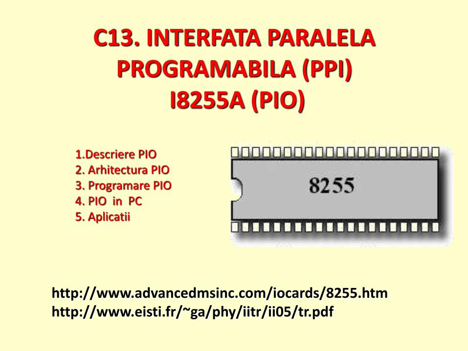
C13. INTERFATA PARALELA PROGRAMABILA (PPI)
I8255A (PIO)
1.Descriere PIO 2. Arhitectura PIO 3. Programare PIO 4. PIO in PC 5. Aplicatii
http://www.advancedmsinc.com/iocards/8255.htm http://www.eisti.fr/~ga/phy/iitr/ii05/tr.pdf
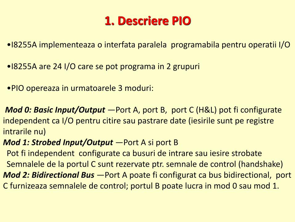
1. Descriere PIO
•I8255A implementeaza o interfata paralela programabila pentru operatii I/O •I8255A are 24 I/O care se pot programa in 2 grupuri
•PIO opereaza in urmatoarele 3 moduri:
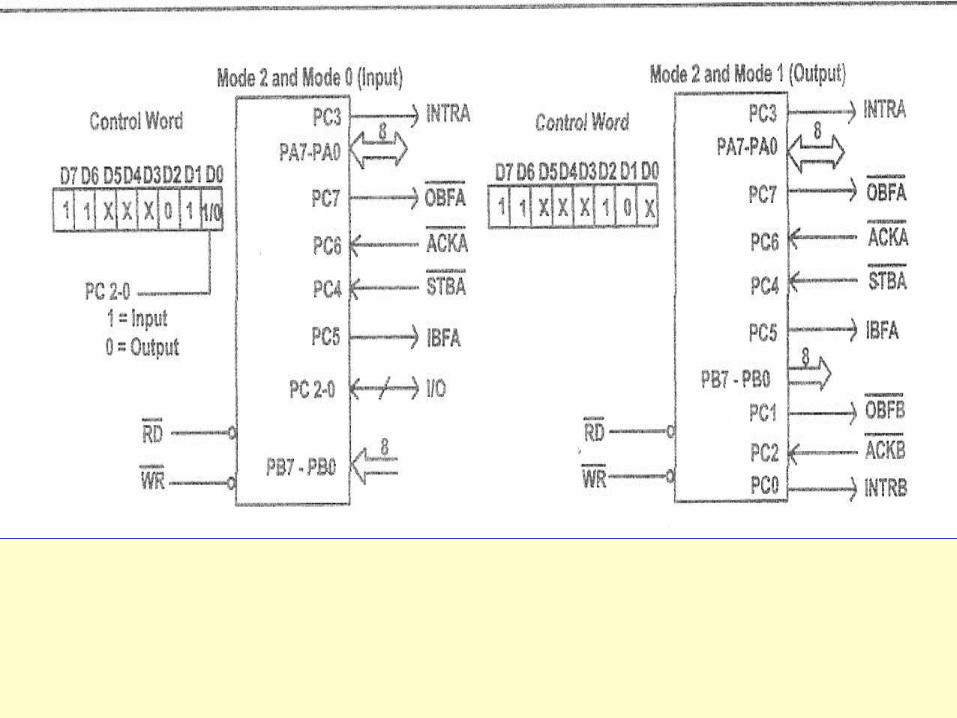
Mod 0: Basic Input/Output —Port A, port B, port C (H&L) pot fi configurate independent ca I/O pentru citire sau pastrare date (iesirile sunt pe registre intrarile nu) Mod 1: Strobed Input/Output —Port A si port B Pot fi independent configurate ca busuri de intrare sau iesire strobate Semnalele de la portul C sunt rezervate ptr. semnale de control (handshake)
Mod 2: Bidirectional Bus —Port A poate fi configurat ca bus bidirectional, port C furnizeaza semnalele de control; portul B poate lucra in mod 0 sau mod 1.
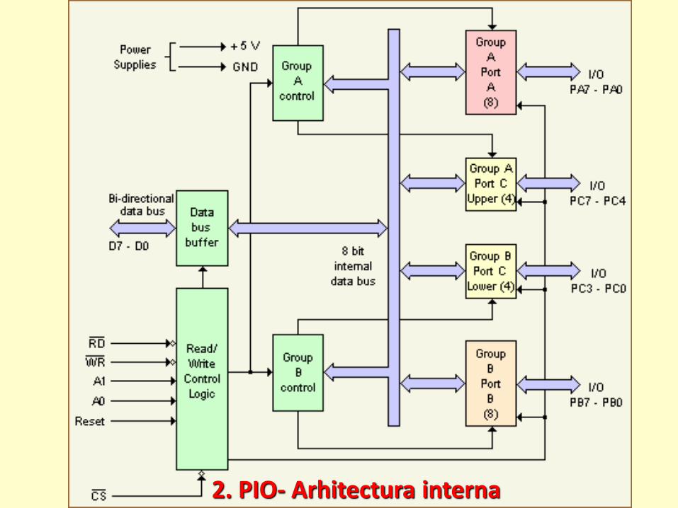
2. PIO- Arhitectura interna
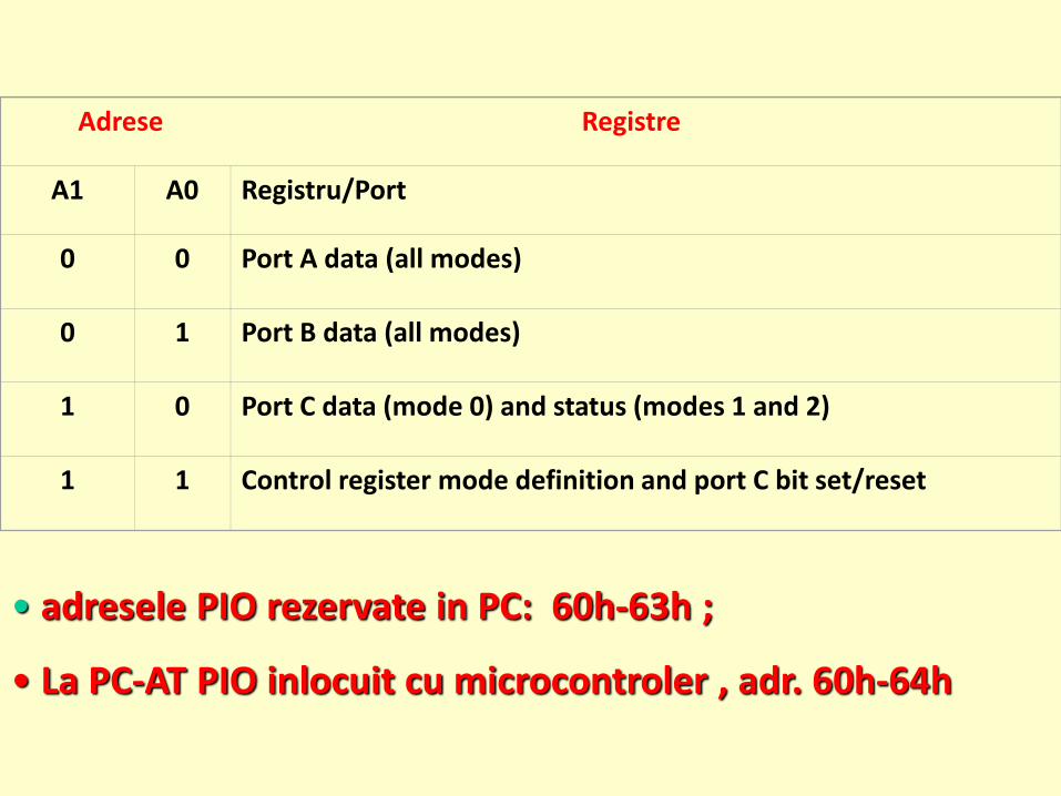
Adrese Registre
A1
A0
Registru/Port
0
0
Port A data (all modes)
0
1
Port B data (all modes)
1
0
Port C data (mode 0) and status (modes 1 and 2)
1
1
Control register mode definition and port C bit set/reset
• adresele PIO rezervate in PC: 60h-63h ;
• La PC-AT PIO inlocuit cu microcontroler , adr. 60h-64h
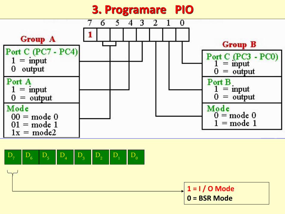
3. Programare PIO
1 = I / O Mode 0 = BSR Mode
D5 D7 D6 D3 D2 D1 D0 D4
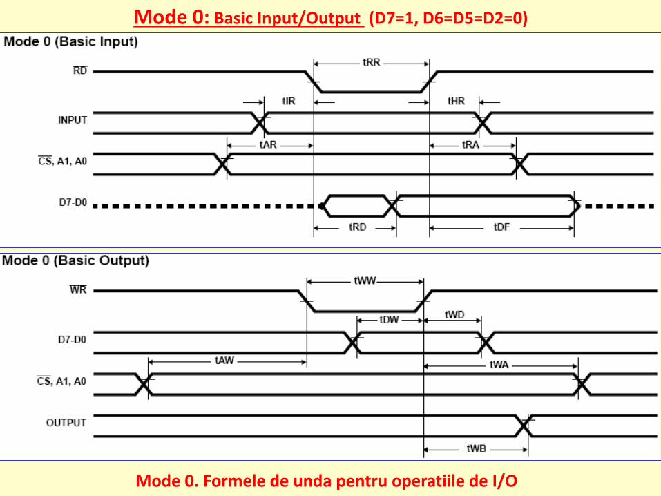
Mode 0. Formele de unda pentru operatiile de I/O
Mode 0: Basic Input/Output (D7=1, D6=D5=D2=0)
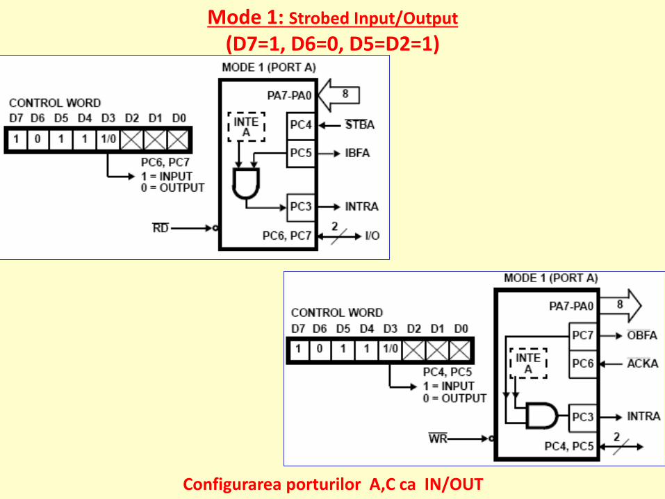
Mode 1: Strobed Input/Output
(D7=1, D6=0, D5=D2=1)
Configurarea porturilor A,C ca IN/OUT
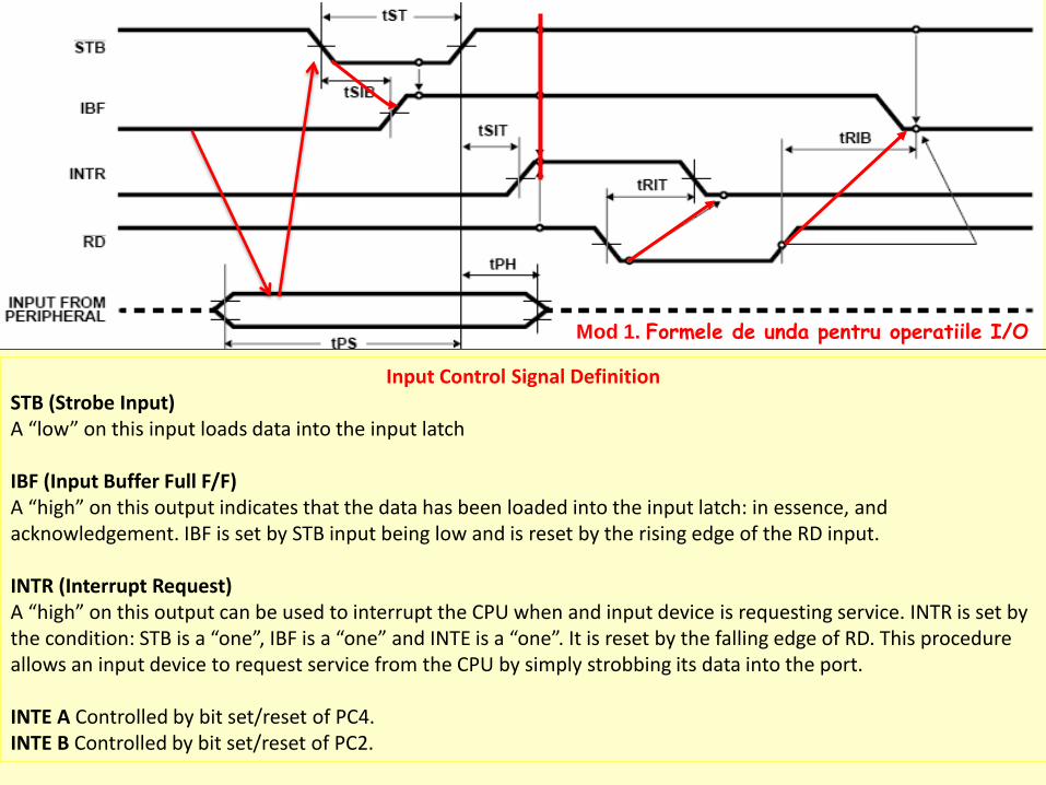
Input Control Signal Definition STB (Strobe Input) A “low” on this input loads data into the input latch IBF (Input Buffer Full F/F) A “high” on this output indicates that the data has been loaded into the input latch: in essence, and acknowledgement. IBF is set by STB input being low and is reset by the rising edge of the RD input. INTR (Interrupt Request) A “high” on this output can be used to interrupt the CPU when and input device is requesting service. INTR is set by the condition: STB is a “one”, IBF is a “one” and INTE is a “one”. It is reset by the falling edge of RD. This procedure allows an input device to request service from the CPU by simply strobbing its data into the port. INTE A Controlled by bit set/reset of PC4. INTE B Controlled by bit set/reset of PC2.
Mod 1. Formele de unda pentru operatiile I/O
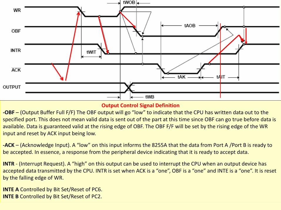
Output Control Signal Definition -OBF – (Output Buffer Full F/F) The OBF output will go “low” to indicate that the CPU has written data out to the specified port. This does not mean valid data is sent out of the part at this time since OBF can go true before data is available. Data is guaranteed valid at the rising edge of OBF. The OBF F/F will be set by the rising edge of the WR input and reset by ACK input being low.
-ACK – (Acknowledge Input). A “low” on this input informs the 8255A that the data from Port A /Port B is ready to be accepted. In essence, a response from the peripheral device indicating that it is ready to accept data.
INTR - (Interrupt Request). A “high” on this output can be used to interrupt the CPU when an output device has accepted data transmitted by the CPU. INTR is set when ACK is a “one”, OBF is a “one” and INTE is a “one”. It is reset by the falling edge of WR.
INTE A Controlled by Bit Set/Reset of PC6. INTE B Controlled by Bit Set/Reset of PC2.
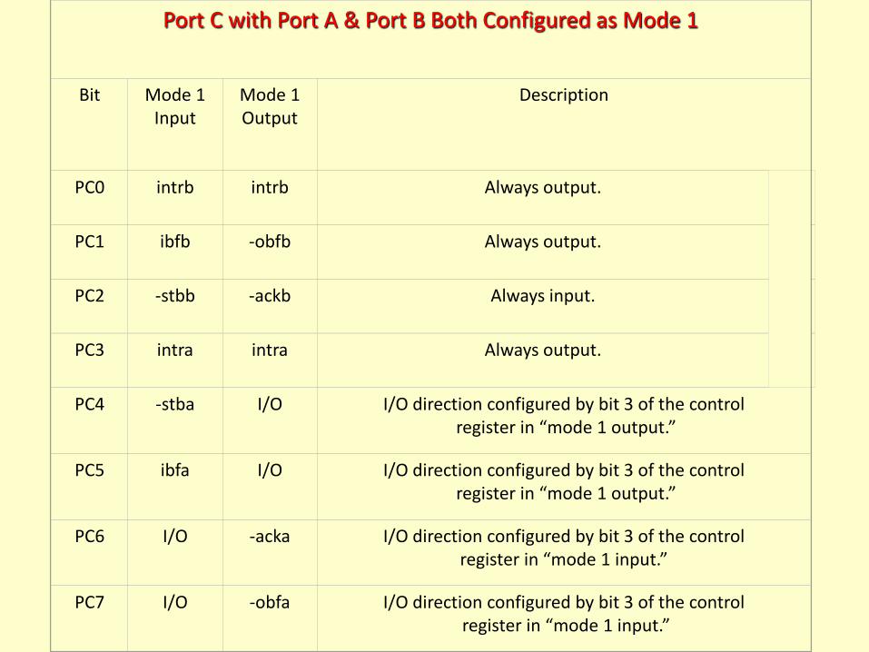
Port C with Port A & Port B Both Configured as Mode 1
Bit
Mode 1 Input
Mode 1 Output
Description
PC0
intrb
intrb
Always output.
PC1
ibfb
-obfb
Always output.
PC2
-stbb
-ackb
Always input.
PC3
intra
intra
Always output.
PC4
-stba
I/O
I/O direction configured by bit 3 of the control register in “mode 1 output.”
PC5
ibfa
I/O
I/O direction configured by bit 3 of the control
register in “mode 1 output.”
PC6
I/O
-acka
I/O direction configured by bit 3 of the control register in “mode 1 input.”
PC7
I/O
-obfa
I/O direction configured by bit 3 of the control
register in “mode 1 input.”

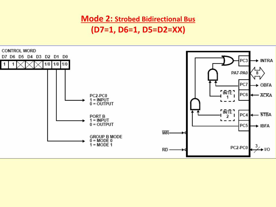
Mode 2: Strobed Bidirectional Bus
(D7=1, D6=1, D5=D2=XX)
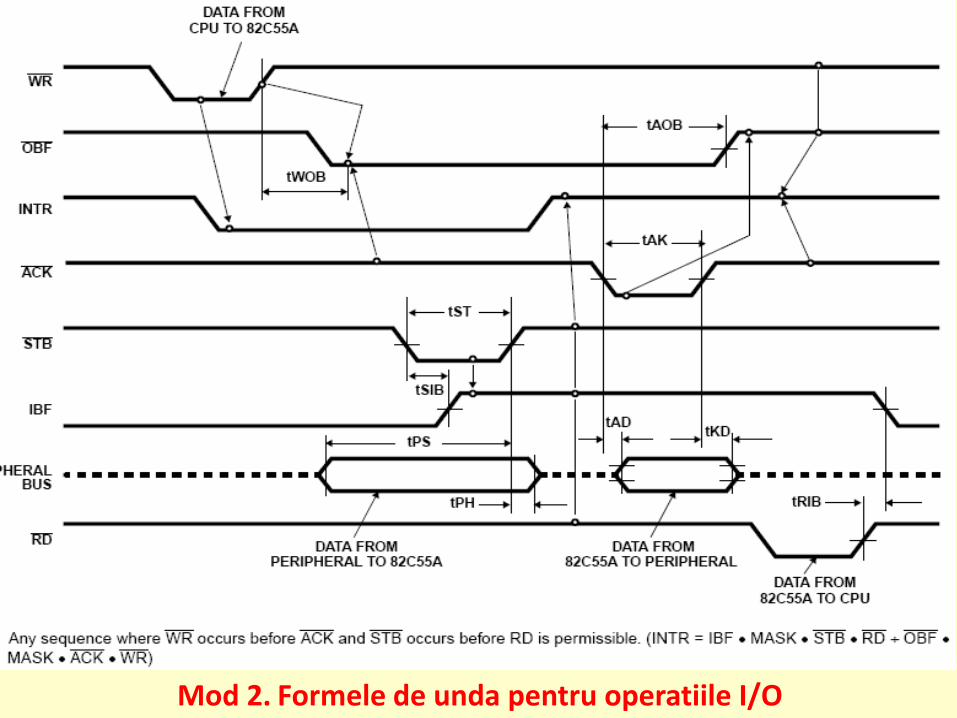
Mod 2. Formele de unda pentru operatiile I/O
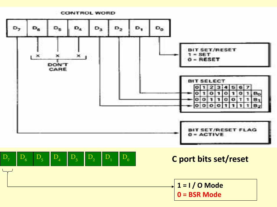
C port bits set/reset
1 = I / O Mode 0 = BSR Mode
D5 D7 D6 D3 D2 D1 D0 D4
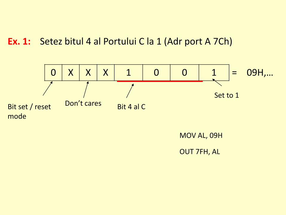
Ex. 1: Setez bitul 4 al Portului C la 1 (Adr port A 7Ch)
0 X X X 1 0 0 1 = 09H,…
Bit set / reset mode
Bit 4 al C
Set to 1
Don’t cares
MOV AL, 09H
OUT 7FH, AL
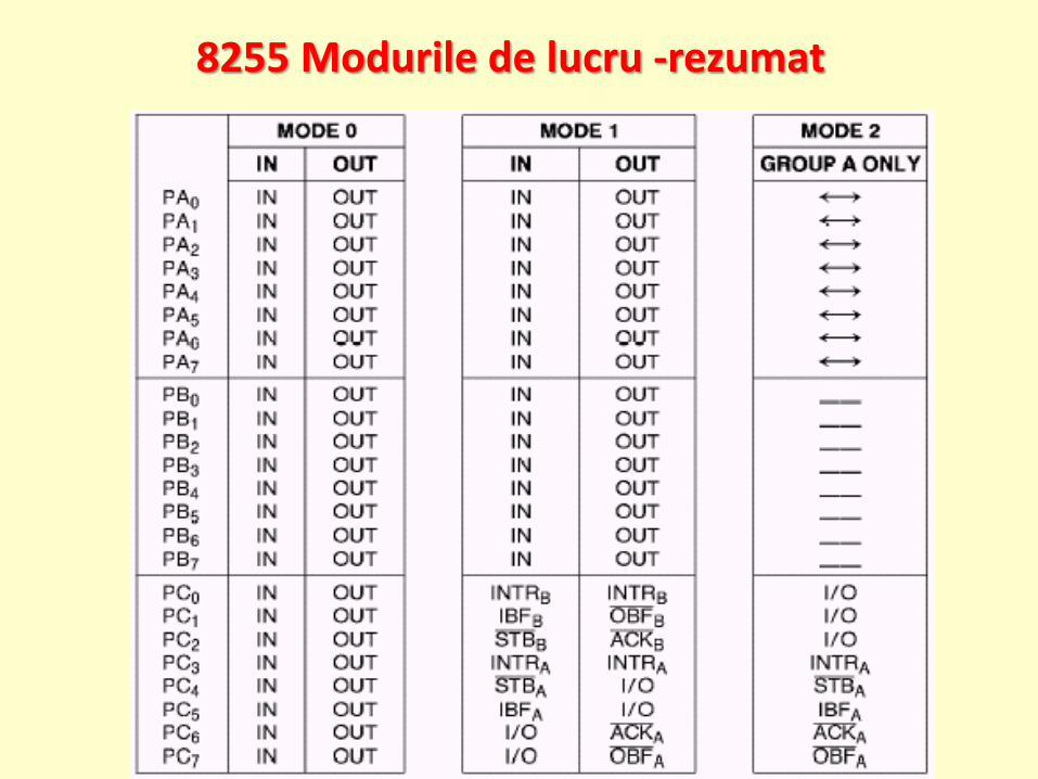
8255 Modurile de lucru -rezumat
A0
A1
D0
D7
A2 System Address Bus
IOW
A7
D0
D7
IOR
WR
RD
A0
A1
CS
A
B
CL
CH
8255A
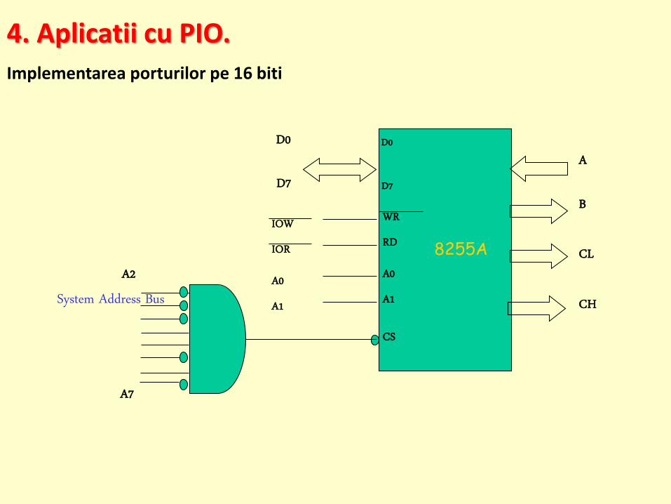
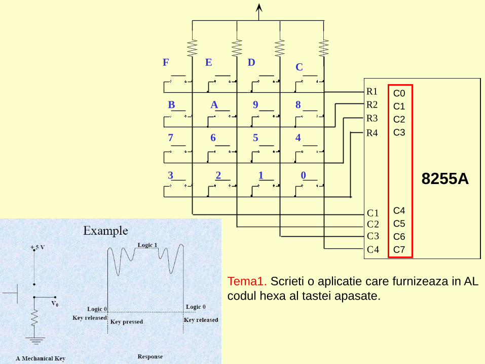
4. Aplicatii cu PIO. Implementarea porturilor pe 16 biti
19
Problema. Interfatati un port pe 16-biti cu 8255 ports la 8086. Adresa portului A este F0h. Solutie. Pentru implementarea unui port de 16biti se folosesc 2x8255. Unul pe partea L a DBUS (D0-D7) , iar celalalt pe partea H a DBUS (D8-D15). Fig. urmatoare.
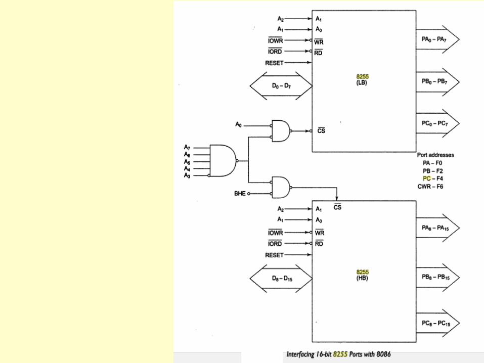
20
C1C2
C3
C4
R1
R2
R3
R4
0 1 2 3
5 6 7
D E F
9 A B
C
8
4
C0
C1
C2
C3
C4
C5
C6
C7
8255A
Tema1. Scrieti o aplicatie care furnizeaza in AL
codul hexa al tastei apasate.
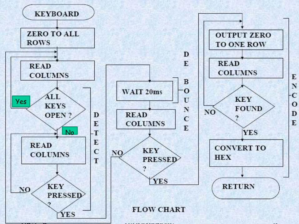
Yes
No
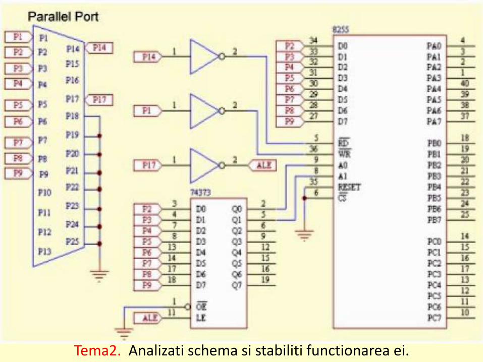
Tema2. Analizati schema si stabiliti functionarea ei.
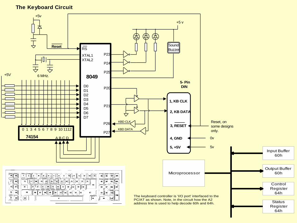
The keyboard controller is 'I/O port' interfaced to the PC/AT as shown. Note, in the circuit how the A2 address line is used to help decode 60h and 64h.
Microprocessor
Input Buffer
60h
Output Buffer
60h
Control
Register
64h
Status
Register
64h
ResetRS
8049
XTAL1
XTAL2
1, KB CLK
2, KB DATA
4, GND
5, +5V
5- Pin
DIN
KBD CLK
KBD DATA
+5v
6 MHz.
Sound
Buzzer
+5 v
0 1 3 4 5 6 7 8 9 10 1112
D0
D1
D2
D3
D4
D5
D6
D7
+5V
A B C D74154
P23
P24
P25
P20
P21
P26
P27
3, RESET
0v
5v
Reset, on
some designs
only.
The Keyboard Circuit
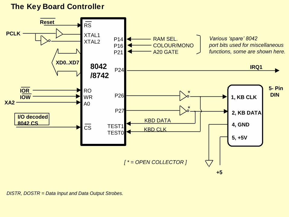
ResetRS
RO
WR
A0
DISTR, DOSTR = Data Input and Data Output Strobes.
IOR
IOW
CS
I/O decoded
8042 CS
8042
/8742
XD0..XD7
XA2
XTAL1
XTAL2
PCLK
*
*
1, KB CLK
2, KB DATA
4, GND
5, +5V
+5
5- Pin
DIN
KBD CLK
KBD DATATEST1
TEST0
P26
P27
[ * = OPEN COLLECTOR ]
P14
P16
P21
RAM SEL.
COLOUR/MONO
A20 GATE
Various ‘spare’ 8042
port bits used for miscellaneous
functions, some are shown here.
P24IRQ1
The Key Board Controller