Embed Size (px)
Citation preview
CDA 4253 FPGA System DesignModeling of Combinational Circuits
Hao ZhengDept of Comp Sci & Eng
USF
2
Reading
➜ P. Chu, FPGA Prototyping by VHDL Examples➺Chapter 3, RT-level combinational circuit➺Sections 3.1 - 3.2, 3.5 - 3.7.
➜ XST User Guide for Virtex-6, Spartan-6, and 7 Series Devices ➺ Chapter 3 and 7
3
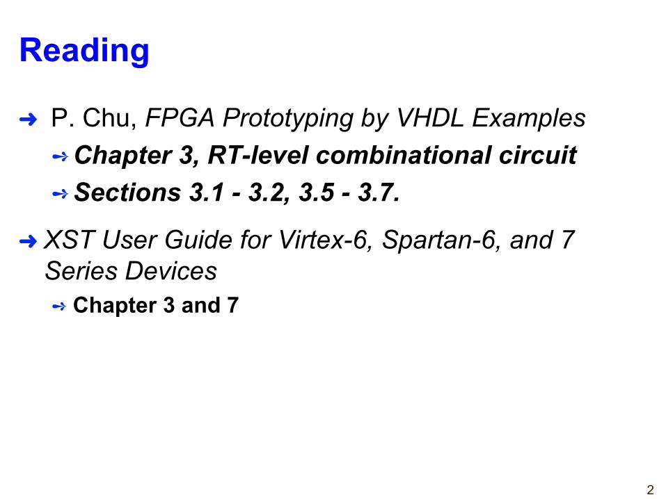
VHDLModelTemplate:Recaplibrary ieee;
use ieee.std_logic_1164.all;
entity entity_name is
port declarations
end [entity] entity_name;
ARCHITECTURE architecture_name OF entity_name IS
Signal & component declarations
BEGIN
Concurrent statements
END [ARCHITECTURE] architecture_name;
4
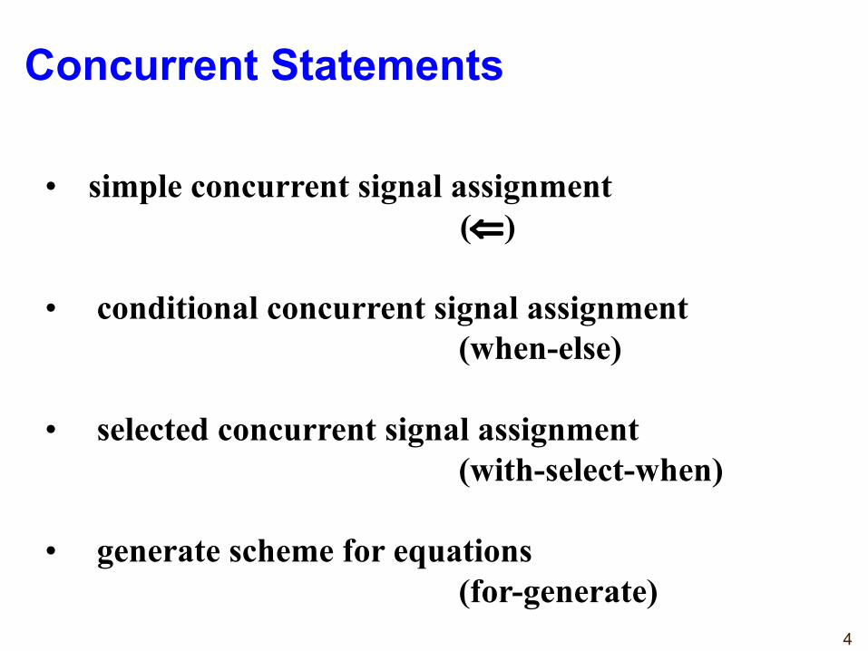
• simple concurrent signal assignment (Ü)
• conditional concurrent signal assignment(when-else)
• selected concurrent signal assignment(with-select-when)
• generate scheme for equations (for-generate)
Concurrent Statements
5
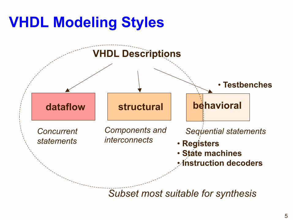
VHDL Modeling Styles
Components andinterconnects
structural
VHDL Descriptions
dataflow
Concurrent statements
behavioral
• Registers• State machines• Instruction decoders
Sequential statements
Subset most suitable for synthesis
• Testbenches
6
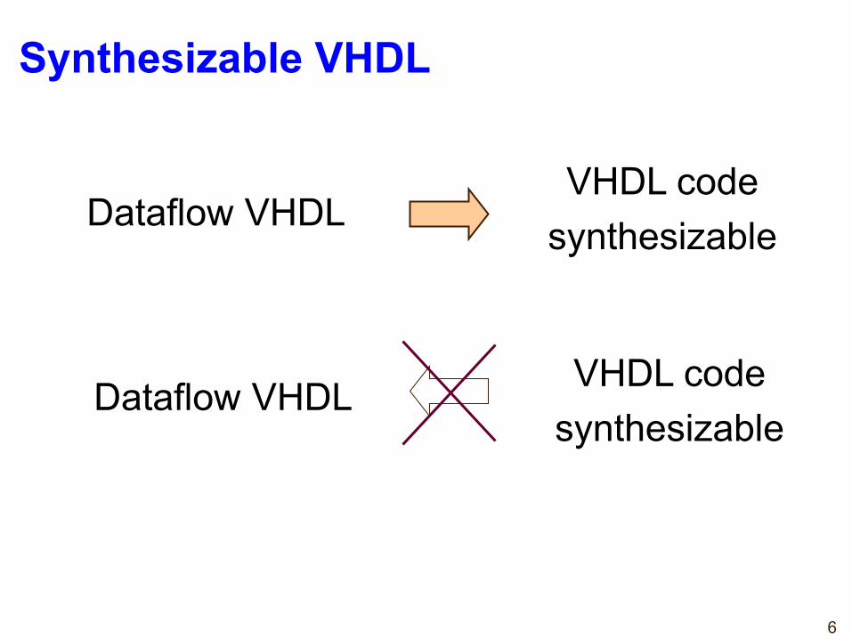
Synthesizable VHDL
Dataflow VHDLVHDL code
synthesizable
VHDL codesynthesizable
Dataflow VHDL
7
CombinationalCircuitBuildingBlocks
8
FixedShifters&Rotators
9
Fixed Logical Shift Right in VHDL
A(3) A(2) A(1) A(0)
‘0’ A(3) A(2) A(1)
A
C
4
4
A
CA srl 1
SIGNAL A : STD_LOGIC_VECTOR(3 DOWNTO 0);
SIGNAL C : STD_LOGIC_VECTOR(3 DOWNTO 0);
srl:logicshiftright C <= A srl 1
C <= ‘0’ & A(3 downto 1);
10
Fixed Arithmetic Shift Right in VHDL
A(3) A(2) A(1) A(0)
A(3) A(2) A(1)
A
C <= A sra 1
c <= A(3) & A(3 downto 1)
C
4
4
A
CA sra 1
A(3)
SIGNAL A : STD_LOGIC_VECTOR(3 DOWNTO 0);
SIGNAL C : STD_LOGIC_VECTOR(3 DOWNTO 0);
sra:arithmeticshiftleft
11
Fixed Rotation in VHDL
A(3) A(2) A(1) A(0)
A(2) A(1) A(0) A(3)
A4
4
A
CA rol 1
SIGNAL A : STD_LOGIC_VECTOR(3 DOWNTO 0);
SIGNAL C : STD_LOGIC_VECTOR(3 DOWNTO 0);
rol: rotation to left C <= A rol 1
C
12
Logic Gates
13
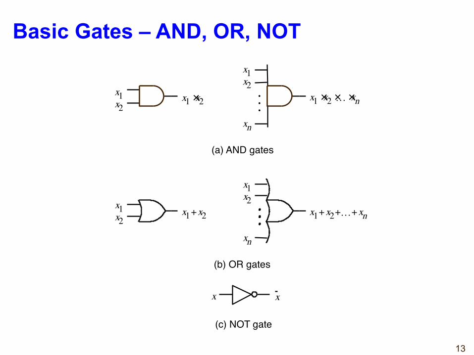
x 1 x 2
x n
x 1 x 2 … x n + + + x 1 x 2
x 1 x 2 +
x 1 x 2
x n
x 1 x 2
x 1 x 2 × x 1 x 2 … x n × × ×
(a) AND gates
(b) OR gates
x x
(c) NOT gate
Basic Gates – AND, OR, NOT
14
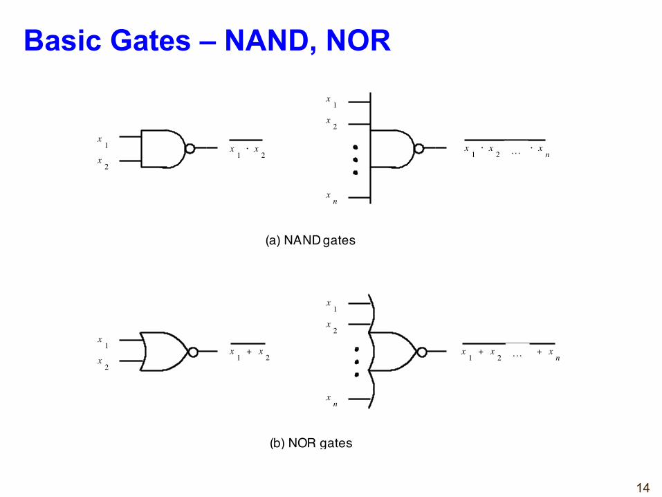
x 1
x 2
x n
x 1
x 2
… x n
+ + + x
1
x 2
x 1
x 2
+
x 1
x 2
x n
x 1
x 2
x 1
x 2
× x 1
x 2
… x n
× × ×
(a) NAND gates
(b) NOR gates
Basic Gates – NAND, NOR
…
…
15
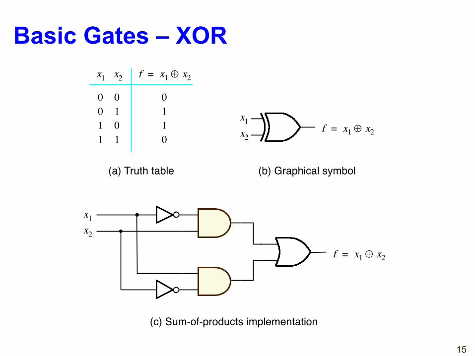
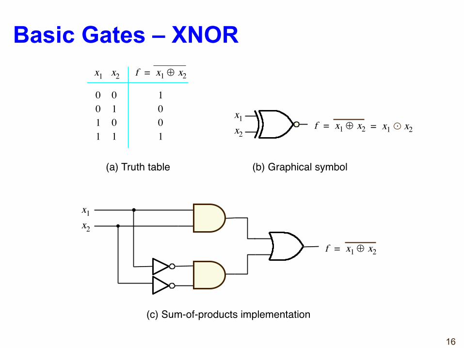
(b) Graphical symbol(a) Truth table
0 0 1 1
0 1 0 1
0 1 1 0
x 1 x 2
x 1 x 2
f x 1 x 2 Å =
f x 1 x 2 Å =
(c) Sum-of-products implementation
f x 1 x 2 Å =
x 1 x 2
Basic Gates – XOR
16
(b) Graphical symbol(a) Truth table
0 0 1 1
0 1 0 1
1 0 0 1
x 1 x 2
x 1 x 2
f x 1 x 2 Å =
f x 1 x 2 Å =
(c) Sum-of-products implementation
f x 1 x 2 Å =
x 1 x 2
x 1 x 2 = .
Basic Gates – XNOR
17
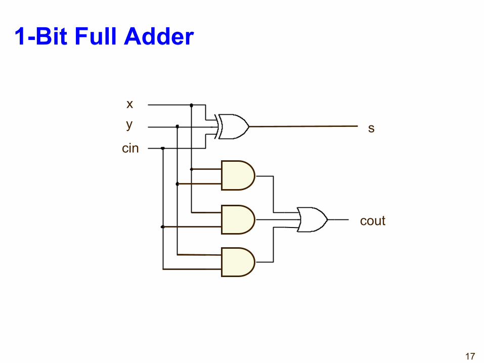
xy
cins
cout
1-Bit Full Adder
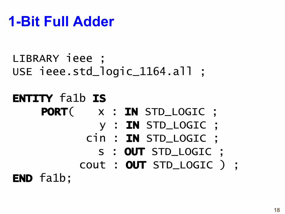
18
LIBRARY ieee ;USE ieee.std_logic_1164.all ;
ENTITY fa1b ISPORT( x : IN STD_LOGIC ;
y : IN STD_LOGIC ; cin : IN STD_LOGIC ;s : OUT STD_LOGIC ;
cout : OUT STD_LOGIC ) ;END fa1b;
1-Bit Full Adder
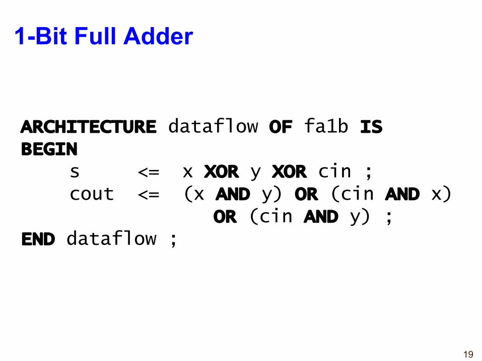
19
ARCHITECTURE dataflow OF fa1b ISBEGIN
s <= x XOR y XOR cin ;cout <= (x AND y) OR (cin AND x)
OR (cin AND y) ;END dataflow ;
1-Bit Full Adder
20
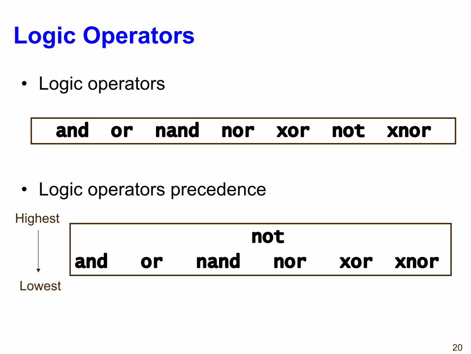
Logic Operators
• Logic operators
• Logic operators precedence
and or nand nor xor not xnor
not
and or nand nor xor xnor
Highest
Lowest
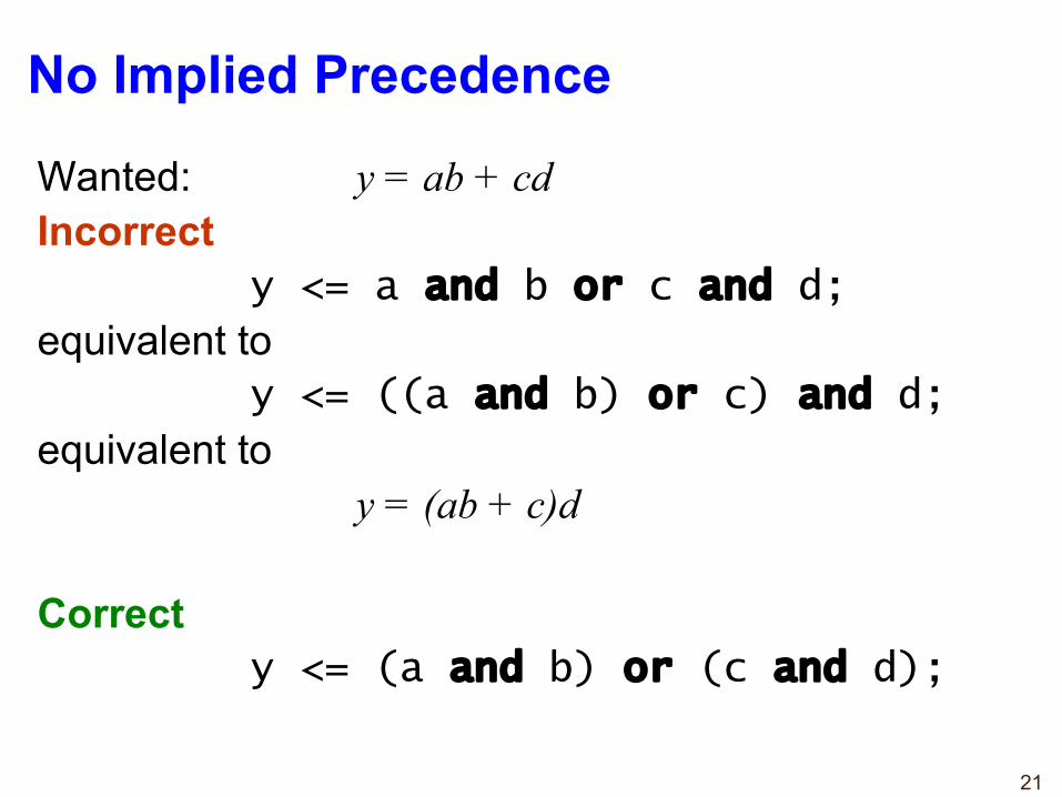
21
Wanted: y = ab + cdIncorrect
y <= a and b or c and d;
equivalent toy <= ((a and b) or c) and d;
equivalent toy = (ab + c)d
Correcty <= (a and b) or (c and d);
No Implied Precedence
22
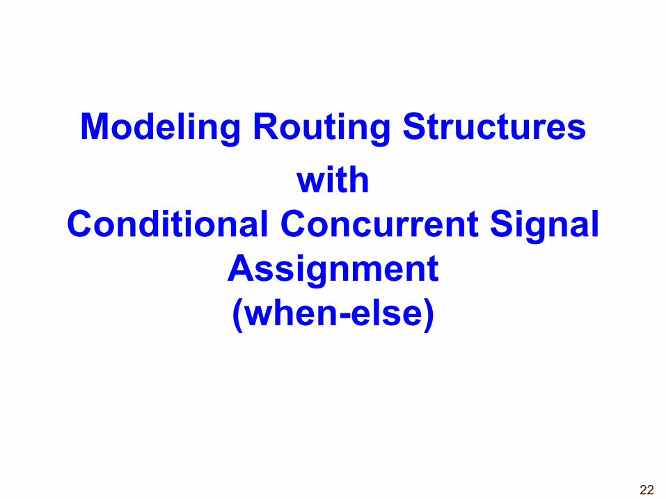
Modeling Routing Structureswith
Conditional Concurrent Signal Assignment(when-else)
23
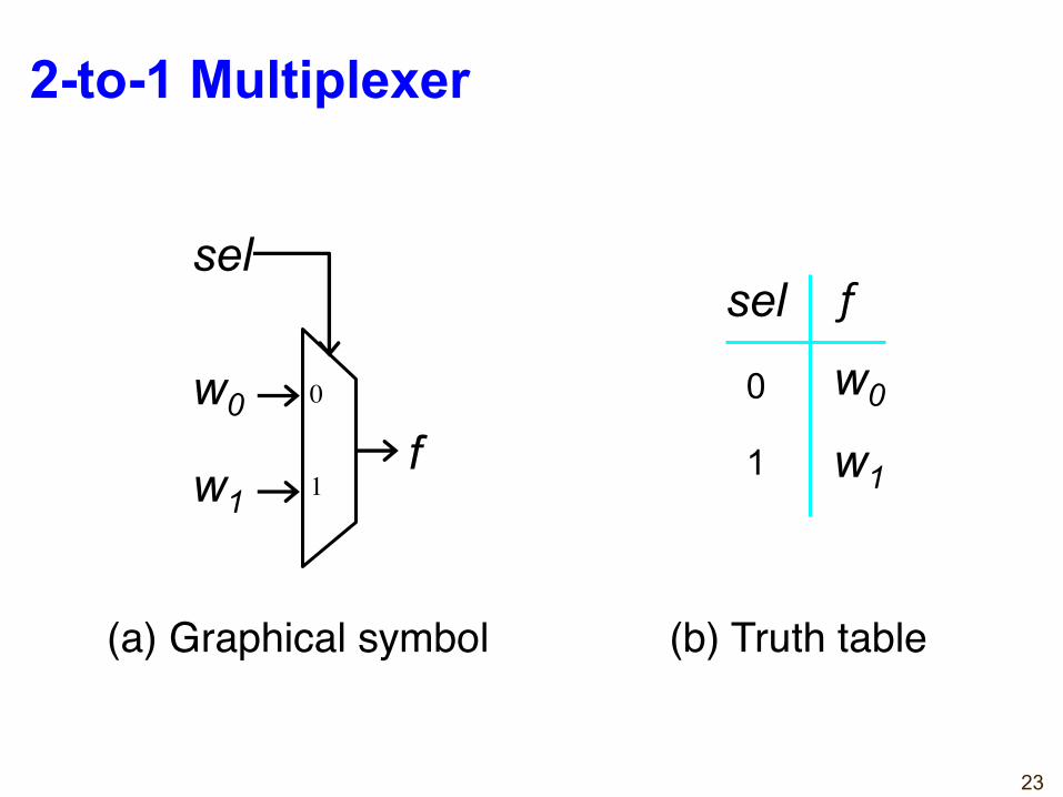
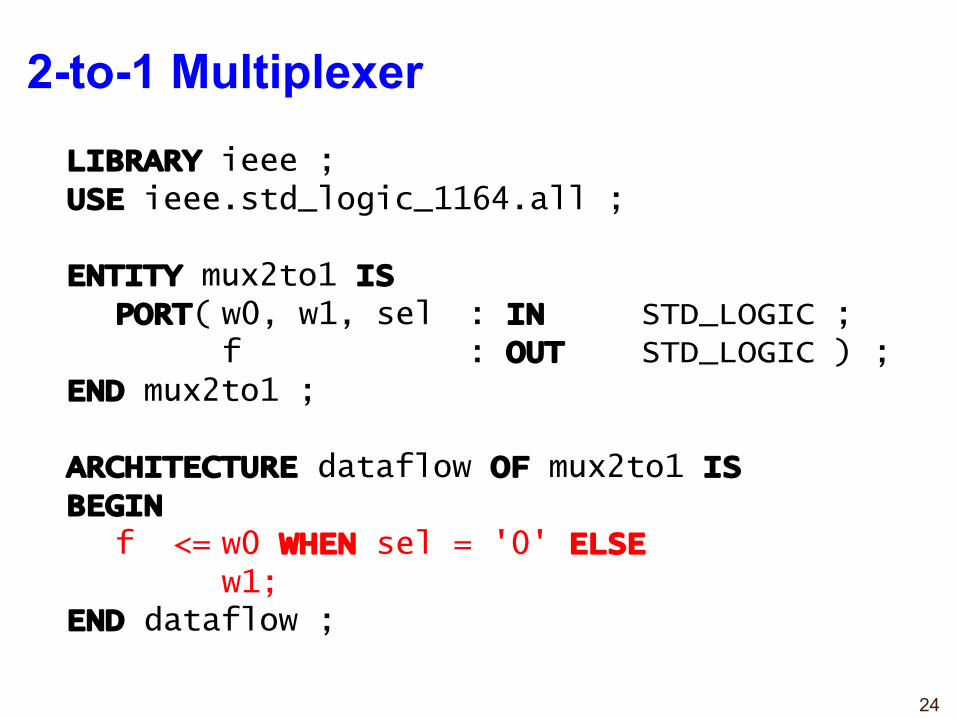
2-to-1 Multiplexer
(a) Graphical symbol (b) Truth table
fsel
f
sel
w0 0
1w1
0
1
w0
w1
24
2-to-1 MultiplexerLIBRARY ieee ;USE ieee.std_logic_1164.all ;
ENTITY mux2to1 ISPORT( w0, w1, sel : IN STD_LOGIC ;
f : OUT STD_LOGIC ) ;END mux2to1 ;
ARCHITECTURE dataflow OF mux2to1 ISBEGIN
f <= w0 WHEN sel = '0' ELSE w1;
END dataflow ;
25
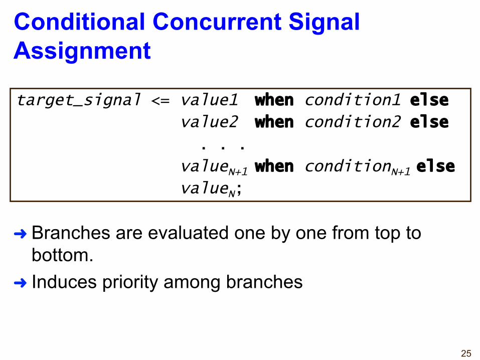
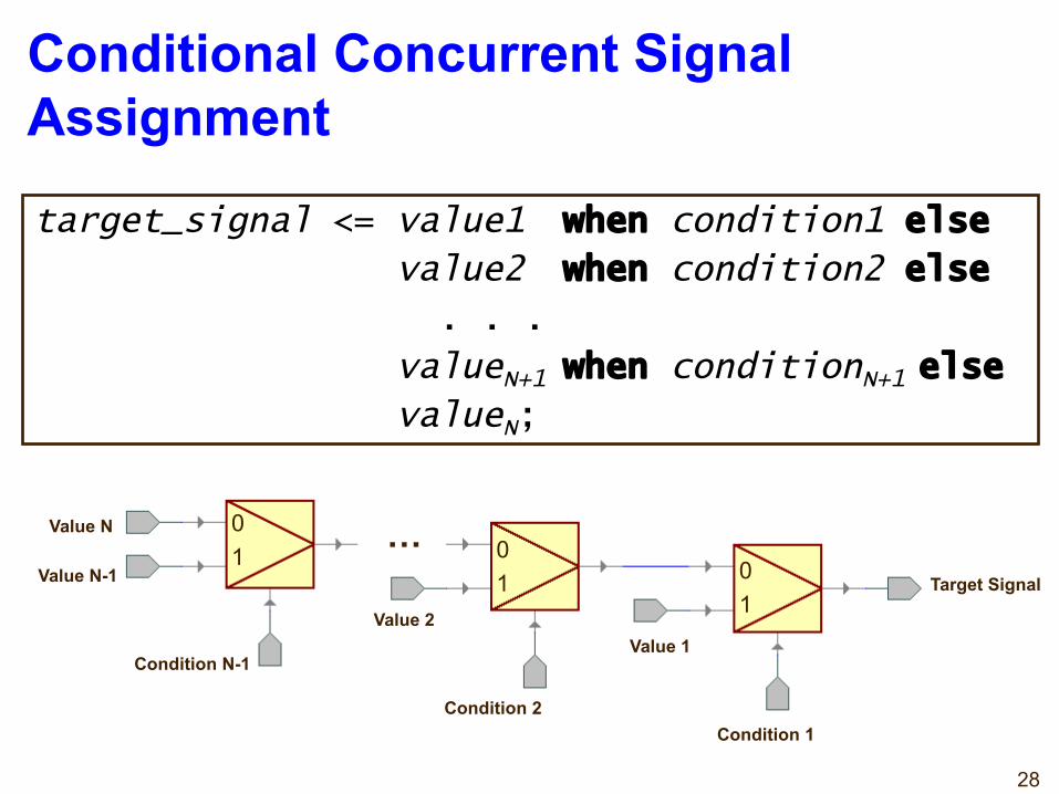
Conditional Concurrent Signal Assignment
➜ Branches are evaluated one by one from top to bottom.
➜ Induces priority among branches
target_signal <= value1 when condition1 else
value2 when condition2 else
. . .
valueN+1 when conditionN+1 else
valueN;
26
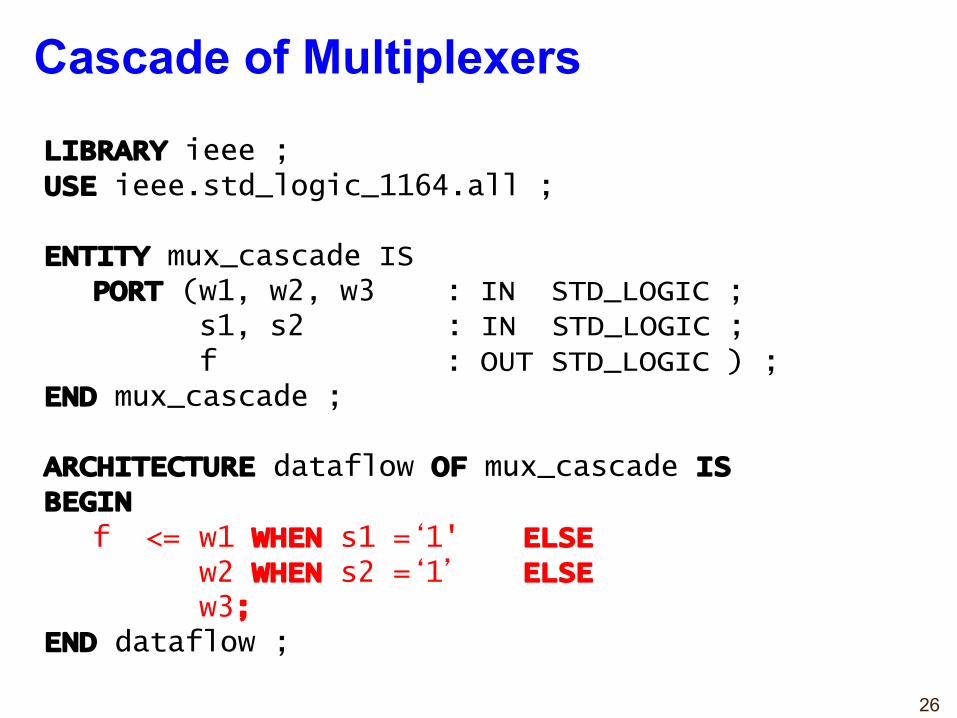
Cascade of Multiplexers
LIBRARY ieee ;USE ieee.std_logic_1164.all ;
ENTITY mux_cascade ISPORT (w1, w2, w3 : IN STD_LOGIC ;
s1, s2 : IN STD_LOGIC ;f : OUT STD_LOGIC ) ;
END mux_cascade ;
ARCHITECTURE dataflow OF mux_cascade ISBEGIN
f <= w1 WHEN s1 =‘1' ELSE w2 WHEN s2 =‘1’ ELSEw3;
END dataflow ;
27
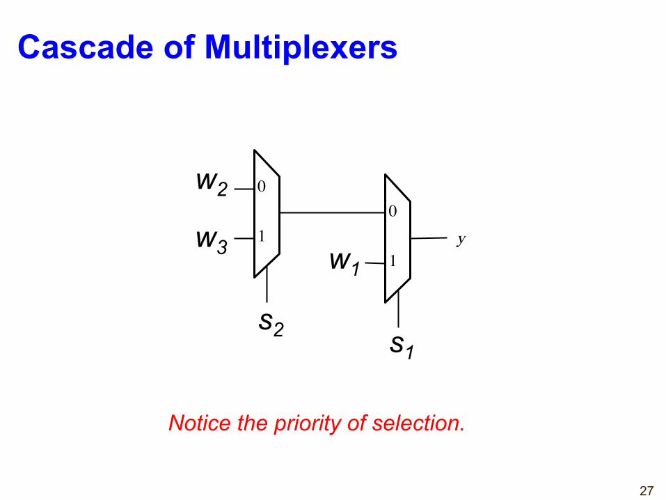
Cascade of Multiplexers
0
1
0
1 y
Notice the priority of selection.
w3
w2
w1
s1s2
28
.…Value N
Value N-1
Condition N-1
Condition 2Condition 1
Value 2Value 1
Target Signal
…01
01
01
Conditional Concurrent Signal Assignment
target_signal <= value1 when condition1 else
value2 when condition2 else
. . .
valueN+1 when conditionN+1 else
valueN;
29
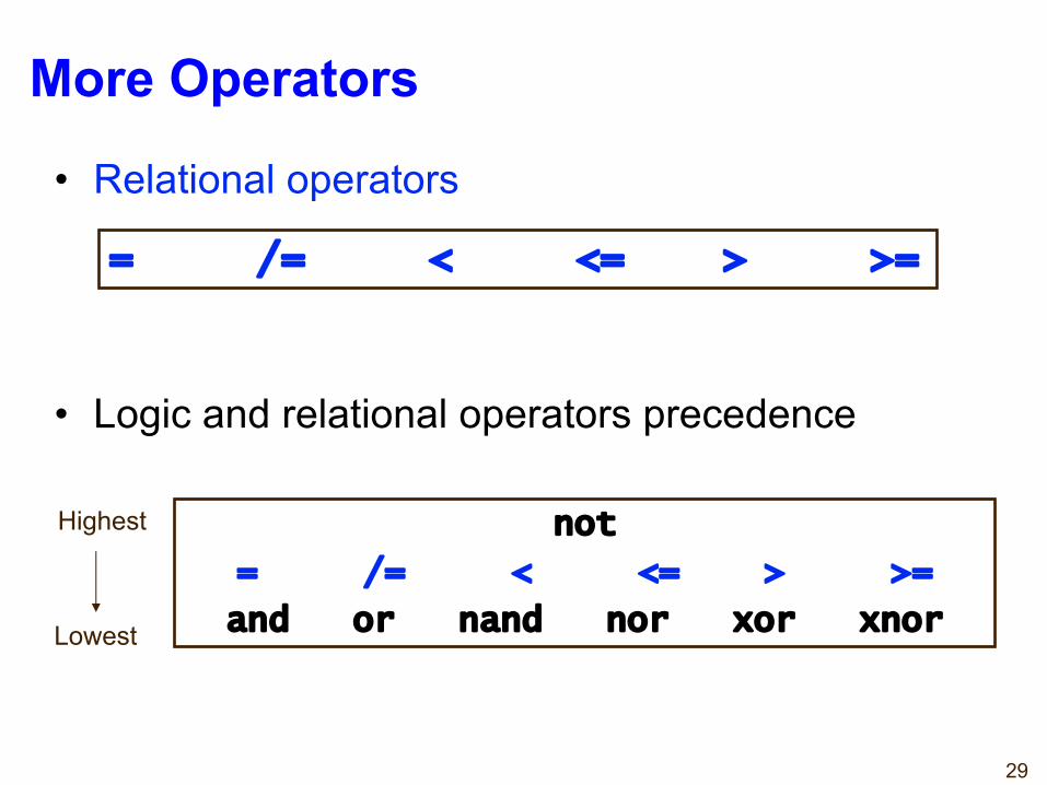
More Operators
• Relational operators
• Logic and relational operators precedence
= /= < <= > >=
not
= /= < <= > >=
and or nand nor xor xnor
Highest
Lowest
30
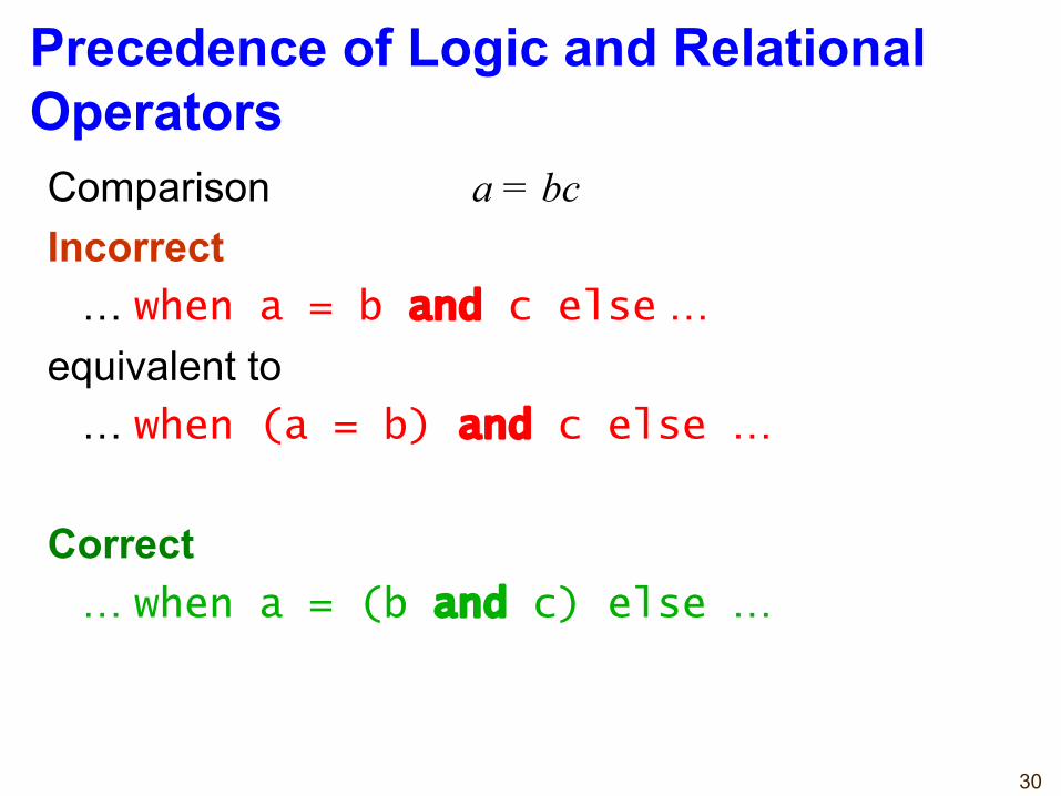
Precedence of Logic and Relational Operators Comparison a = bcIncorrect
… when a = b and c else …equivalent to
… when (a = b) and c else …
Correct… when a = (b and c) else …
31
Modeling Routing Structureswith
Selected Concurrent Signal Assignment
(with-select-when)
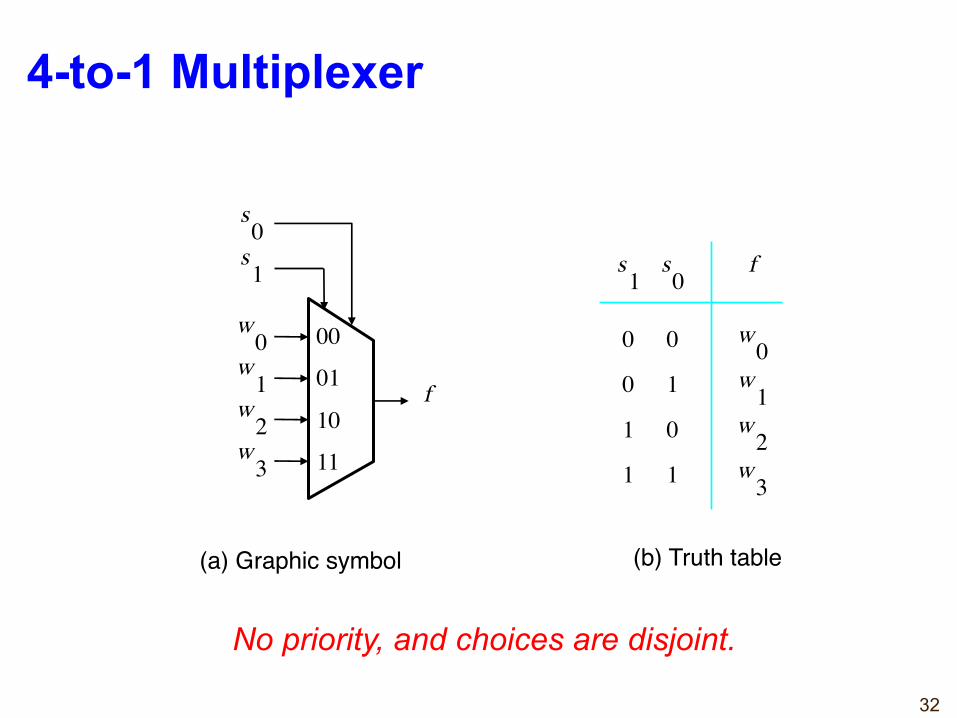
32
f
s 1
w 0
w 1
00
01
(b) Truth table
w 0
w 1
s 0
w 2
w 3
10
11
0
0
1
1
1
0
1
f s 1
0
s 0
w 2
w 3
(a) Graphic symbol
No priority, and choices are disjoint.
4-to-1 Multiplexer
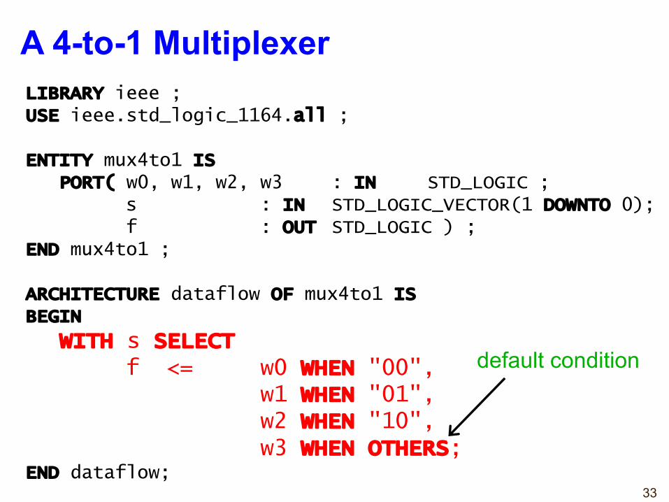
33
LIBRARY ieee ;USE ieee.std_logic_1164.all ;
ENTITY mux4to1 ISPORT( w0, w1, w2, w3 : IN STD_LOGIC ;
s : IN STD_LOGIC_VECTOR(1 DOWNTO 0);f : OUT STD_LOGIC ) ;
END mux4to1 ;
ARCHITECTURE dataflow OF mux4to1 ISBEGIN
WITH s SELECT
f <= w0 WHEN "00",w1 WHEN "01",w2 WHEN "10",w3 WHEN OTHERS;
END dataflow;
A 4-to-1 Multiplexer
default condition
34
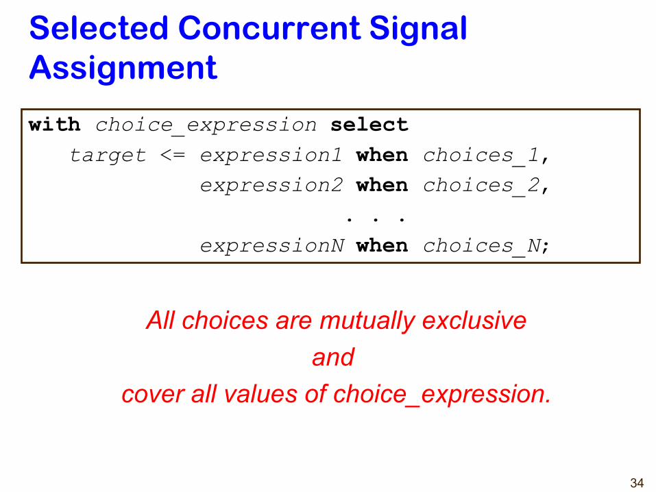
Selected Concurrent SignalAssignment
with choice_expression selecttarget <= expression1 when choices_1,
expression2 when choices_2,. . .
expressionN when choices_N;
All choices are mutually exclusiveand
cover all values of choice_expression.
35
Selected Concurrent Signal Assignmentwith choice_expression select
target <= expression1 when choices_1,expression2 when choices_2,
. . .expressionN when choices_N;
choices_1
choices_2
choices_N
expression1
target_signal
choice expression
expression2
expressionN
36
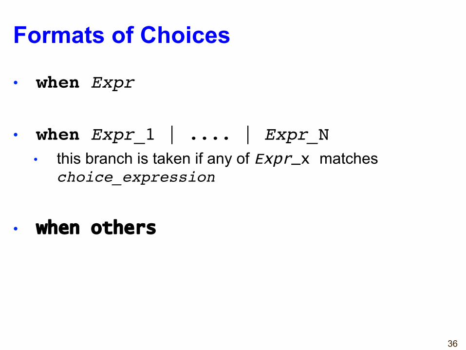
Formats of Choices
• when Expr
• when Expr_1 | .... | Expr_N• this branch is taken if any of Expr_x matches
choice_expression
• when others
37
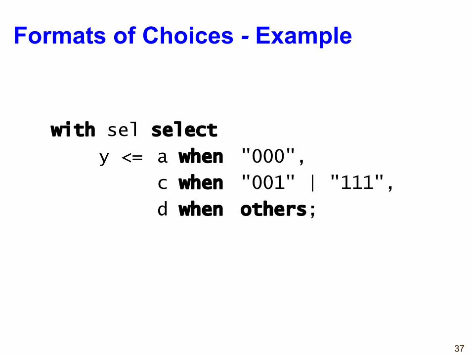
Formats of Choices - Example
with sel select
y <= a when "000",
c when "001" | "111",
d when others;
38
Decoders
39
2-to-4 Decoder
0
0
1
1
1
0
1
y 3
w 1
0
w 0
x x
1
1
0
1
1
En
0
0
1
0
0
y 2
0
1
0
0
0
y 1
1
0
0
0
0
y 0
0
0
0
1
0
w 1
En
y 3
w 0
y 2
y 1
y 0
(a) Truth table (b) Graphical symbol
40
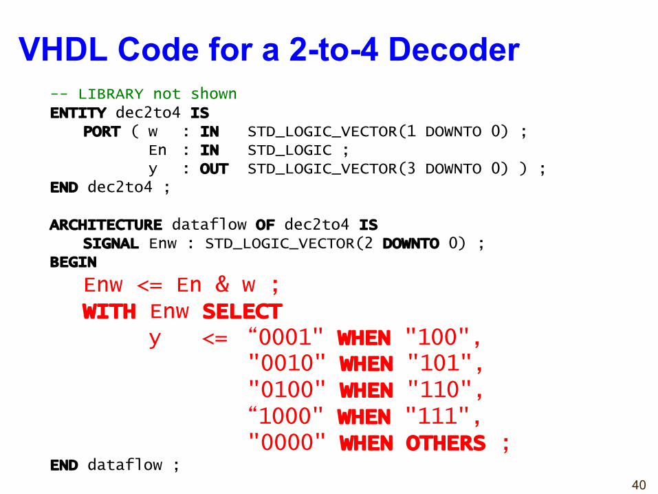
-- LIBRARY not shownENTITY dec2to4 IS
PORT ( w : IN STD_LOGIC_VECTOR(1 DOWNTO 0) ;En : IN STD_LOGIC ;y : OUT STD_LOGIC_VECTOR(3 DOWNTO 0) ) ;
END dec2to4 ;
ARCHITECTURE dataflow OF dec2to4 ISSIGNAL Enw : STD_LOGIC_VECTOR(2 DOWNTO 0) ;
BEGIN
Enw <= En & w ;WITH Enw SELECT
y <= “0001" WHEN "100","0010" WHEN "101","0100" WHEN "110",“1000" WHEN "111","0000" WHEN OTHERS ;
END dataflow ;
VHDL Code for a 2-to-4 Decoder
41
Encoders
42
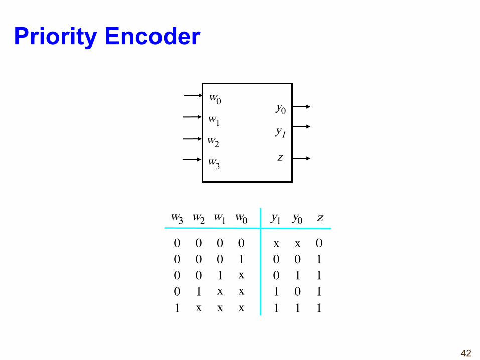
Priority Encoder
w 0
w 3
y 0
y 1
x001
010
w0 y1
x
y0
1 1
01
1
11
z
1xx
0
x
w1
01x
0
x
w2
001
0
x
w3
000
0
1
z
w 1
w 2
43
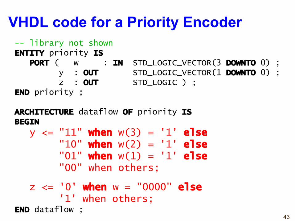
VHDL code for a Priority Encoder-- library not shownENTITY priority IS
PORT ( w : IN STD_LOGIC_VECTOR(3 DOWNTO 0) ;y : OUT STD_LOGIC_VECTOR(1 DOWNTO 0) ;z : OUT STD_LOGIC ) ;
END priority ;
ARCHITECTURE dataflow OF priority ISBEGIN
y <= "11" when w(3) = '1’ else"10" when w(2) = '1' else"01" when w(1) = '1' else"00" when others;
z <= '0' when w = "0000" else'1' when others;
END dataflow ;
44
Adders
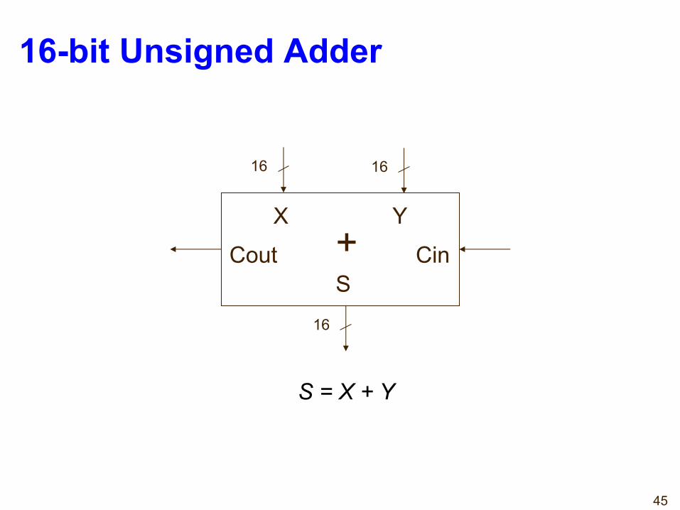
45
16-bit Unsigned Adder
16 16
X Y
16
CinCoutS+
S = X + Y
46
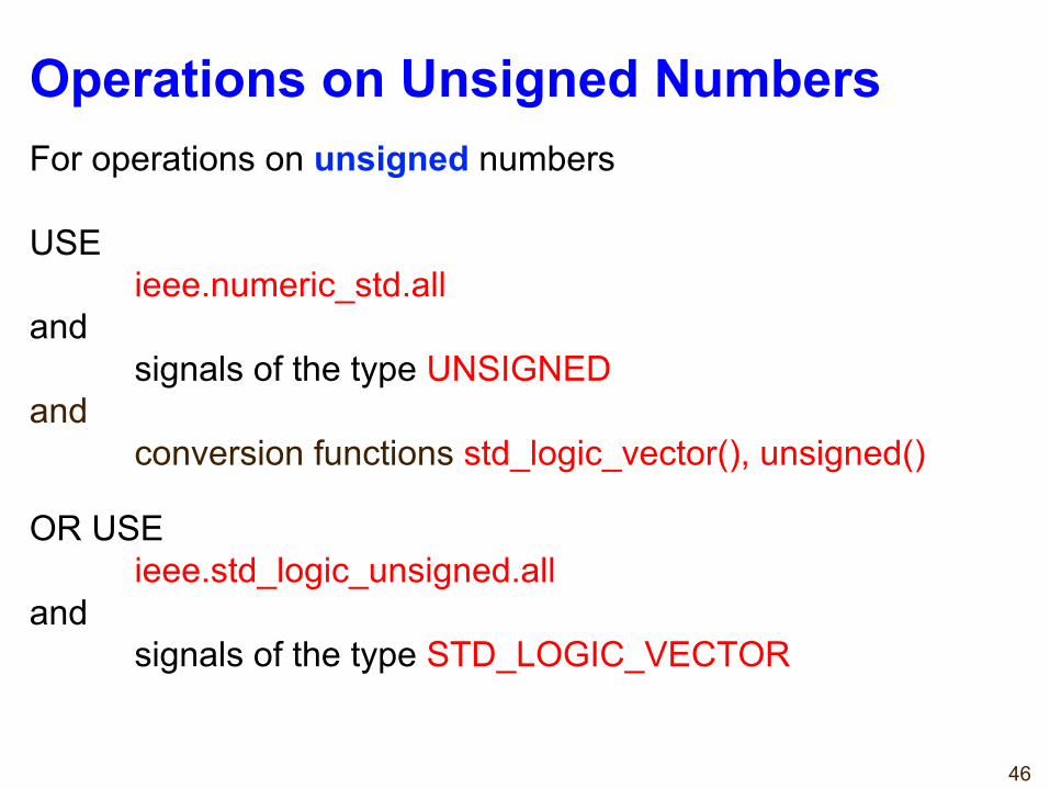
Operations on Unsigned NumbersFor operations on unsigned numbers
USEieee.numeric_std.all
and signals of the type UNSIGNED
and conversion functions std_logic_vector(), unsigned()
OR USEieee.std_logic_unsigned.all
and signals of the type STD_LOGIC_VECTOR
47
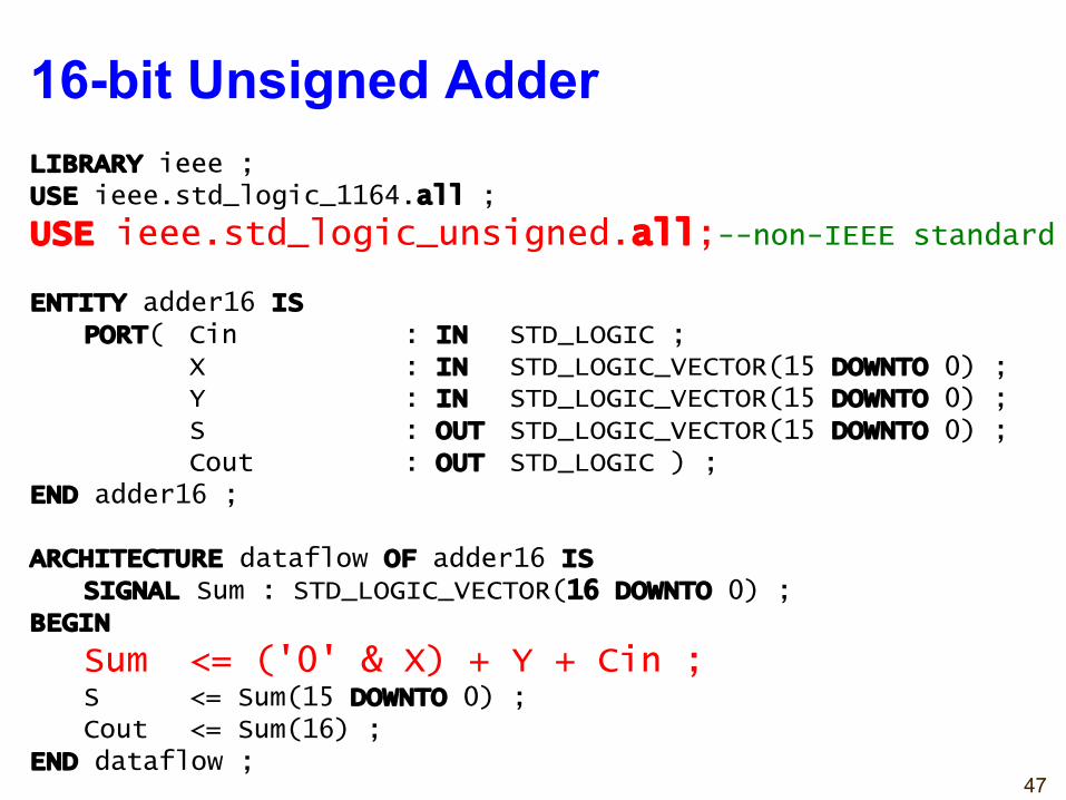
LIBRARY ieee ;USE ieee.std_logic_1164.all ;
USE ieee.std_logic_unsigned.all;--non-IEEE standard
ENTITY adder16 ISPORT( Cin : IN STD_LOGIC ;
X : IN STD_LOGIC_VECTOR(15 DOWNTO 0) ;Y : IN STD_LOGIC_VECTOR(15 DOWNTO 0) ;S : OUT STD_LOGIC_VECTOR(15 DOWNTO 0) ;Cout : OUT STD_LOGIC ) ;
END adder16 ;
ARCHITECTURE dataflow OF adder16 IS SIGNAL Sum : STD_LOGIC_VECTOR(16 DOWNTO 0) ;
BEGIN
Sum <= ('0' & X) + Y + Cin ;S <= Sum(15 DOWNTO 0) ;Cout <= Sum(16) ;
END dataflow ;
16-bit Unsigned Adder
48
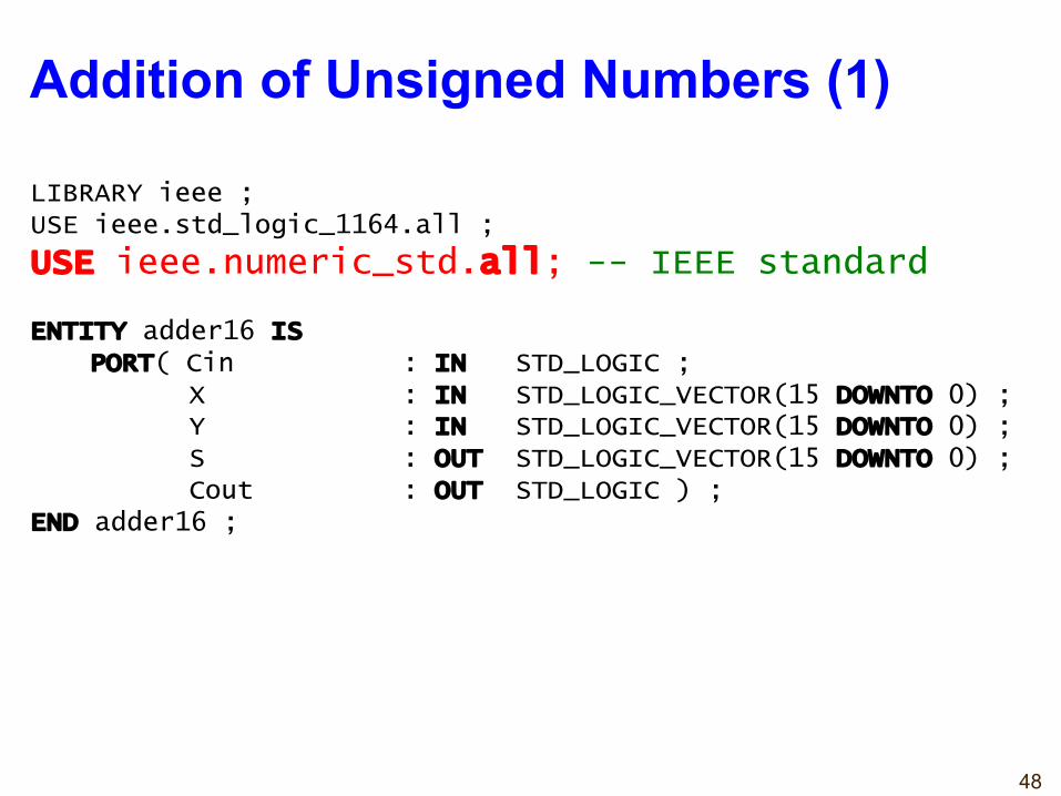
Addition of Unsigned Numbers (1)
LIBRARY ieee ;USE ieee.std_logic_1164.all ;
USE ieee.numeric_std.all; -- IEEE standard
ENTITY adder16 ISPORT( Cin : IN STD_LOGIC ;
X : IN STD_LOGIC_VECTOR(15 DOWNTO 0) ;Y : IN STD_LOGIC_VECTOR(15 DOWNTO 0) ;S : OUT STD_LOGIC_VECTOR(15 DOWNTO 0) ;Cout : OUT STD_LOGIC ) ;
END adder16 ;
49
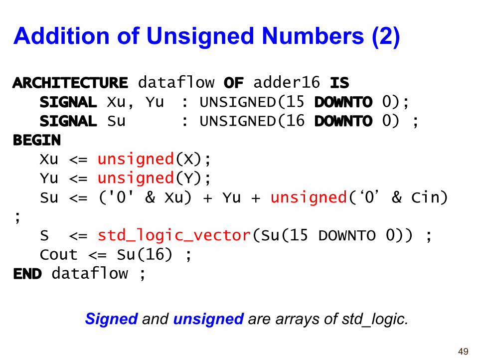
Addition of Unsigned Numbers (2)
ARCHITECTURE dataflow OF adder16 IS SIGNAL Xu, Yu : UNSIGNED(15 DOWNTO 0);SIGNAL Su : UNSIGNED(16 DOWNTO 0) ;
BEGIN
Xu <= unsigned(X);Yu <= unsigned(Y);Su <= ('0' & Xu) + Yu + unsigned(‘0’ & Cin)
;S <= std_logic_vector(Su(15 DOWNTO 0)) ;Cout <= Su(16) ;
END dataflow ;
Signed and unsigned are arrays of std_logic.
50
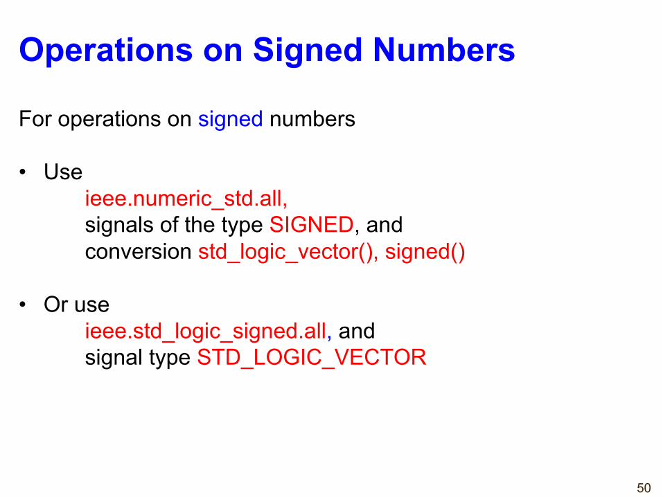
Operations on Signed Numbers
For operations on signed numbers
• Useieee.numeric_std.all,signals of the type SIGNED, andconversion std_logic_vector(), signed()
• Or useieee.std_logic_signed.all, andsignal type STD_LOGIC_VECTOR
51
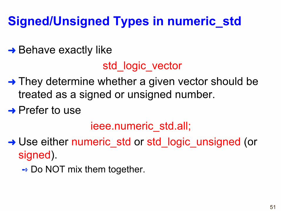
Signed/Unsigned Types in numeric_std
➜ Behave exactly like std_logic_vector
➜ They determine whether a given vector should be treated as a signed or unsigned number.
➜ Prefer to use ieee.numeric_std.all;
➜ Use either numeric_std or std_logic_unsigned (or signed).➺ Do NOT mix them together.
52
Multipliers
53
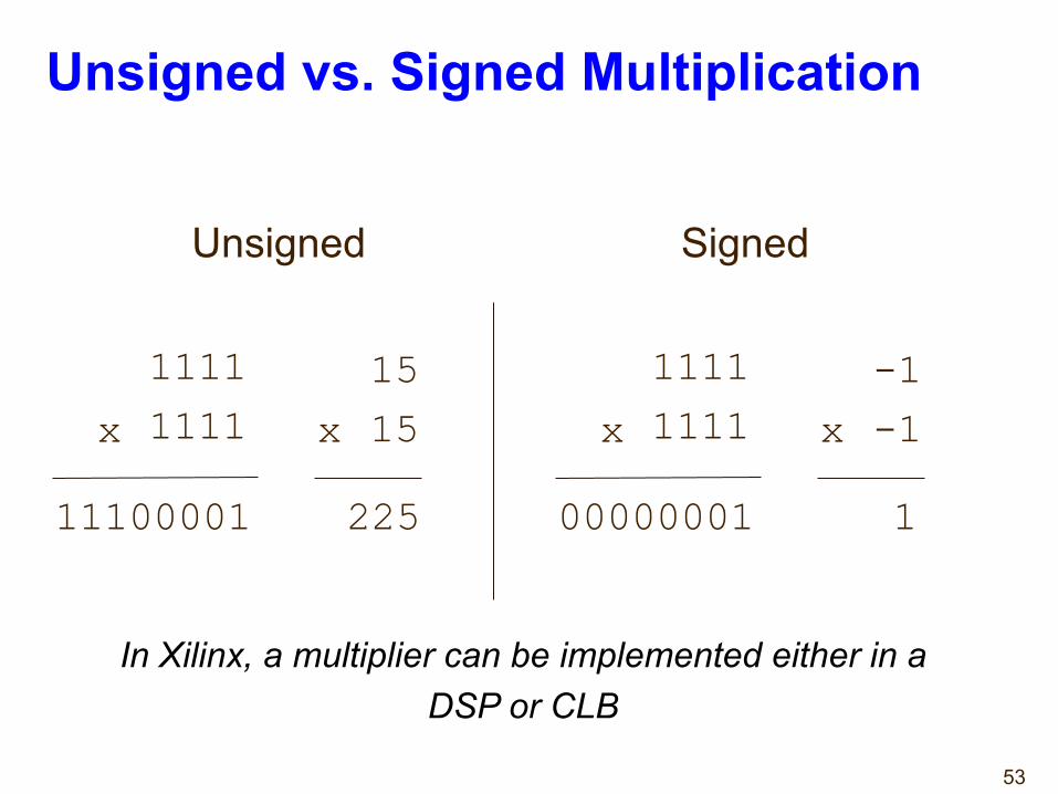
Unsigned vs. Signed Multiplication
1111
1111x
11100001
15
15x
225
1111
1111x
00000001
-1
-1x
1
Unsigned Signed
In Xilinx, a multiplier can be implemented either in a DSP or CLB
54
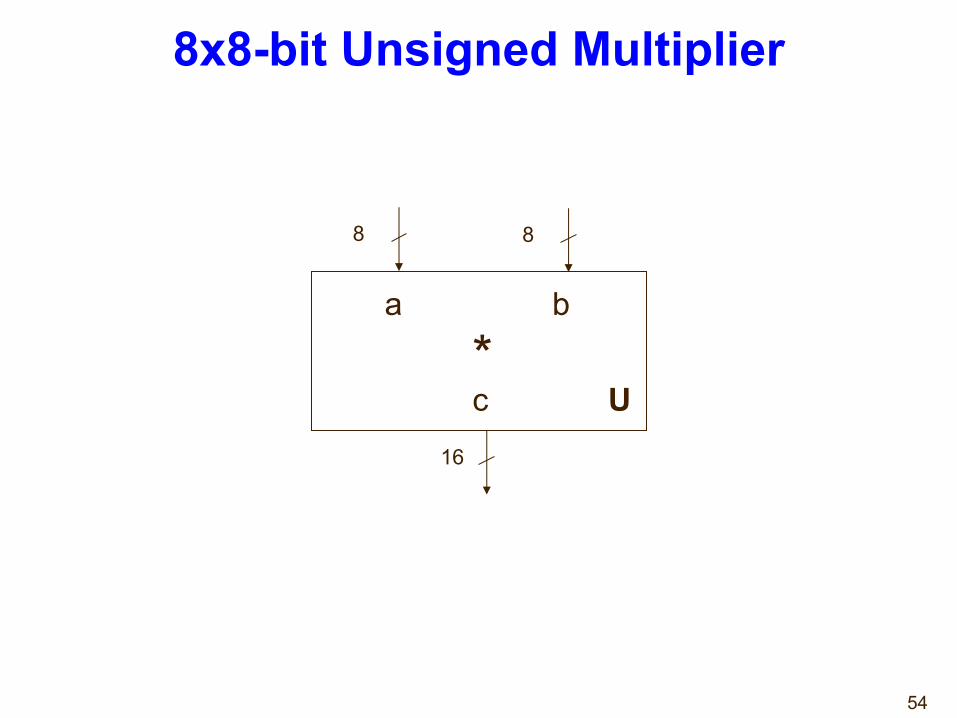
8x8-bit Unsigned Multiplier
8 8
a b
16
c U*
55
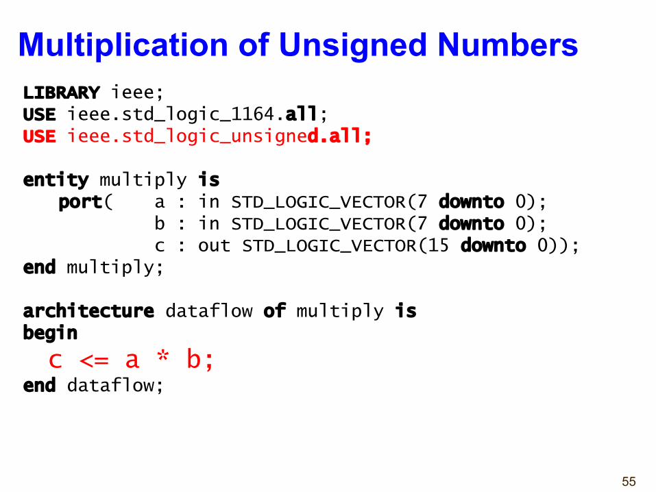
Multiplication of Unsigned NumbersLIBRARY ieee;USE ieee.std_logic_1164.all; USE ieee.std_logic_unsigned.all;
entity multiply isport( a : in STD_LOGIC_VECTOR(7 downto 0);
b : in STD_LOGIC_VECTOR(7 downto 0);c : out STD_LOGIC_VECTOR(15 downto 0));
end multiply;
architecture dataflow of multiply isbegin
c <= a * b;end dataflow;
56
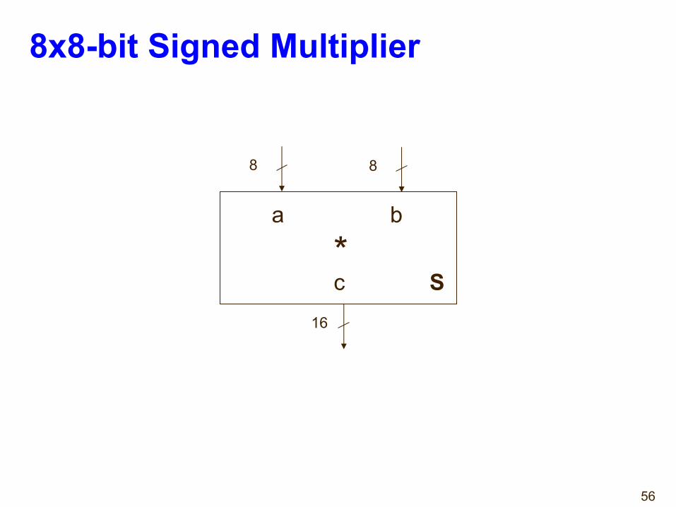
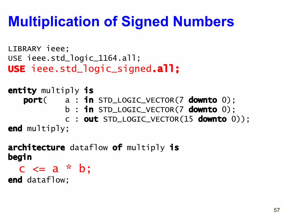
8x8-bit Signed Multiplier
8 8
a b
16
c S*
57
Multiplication of Signed NumbersLIBRARY ieee;USE ieee.std_logic_1164.all;
USE ieee.std_logic_signed.all;
entity multiply isport( a : in STD_LOGIC_VECTOR(7 downto 0);
b : in STD_LOGIC_VECTOR(7 downto 0);c : out STD_LOGIC_VECTOR(15 downto 0));
end multiply;
architecture dataflow of multiply isbegin
c <= a * b;end dataflow;
58
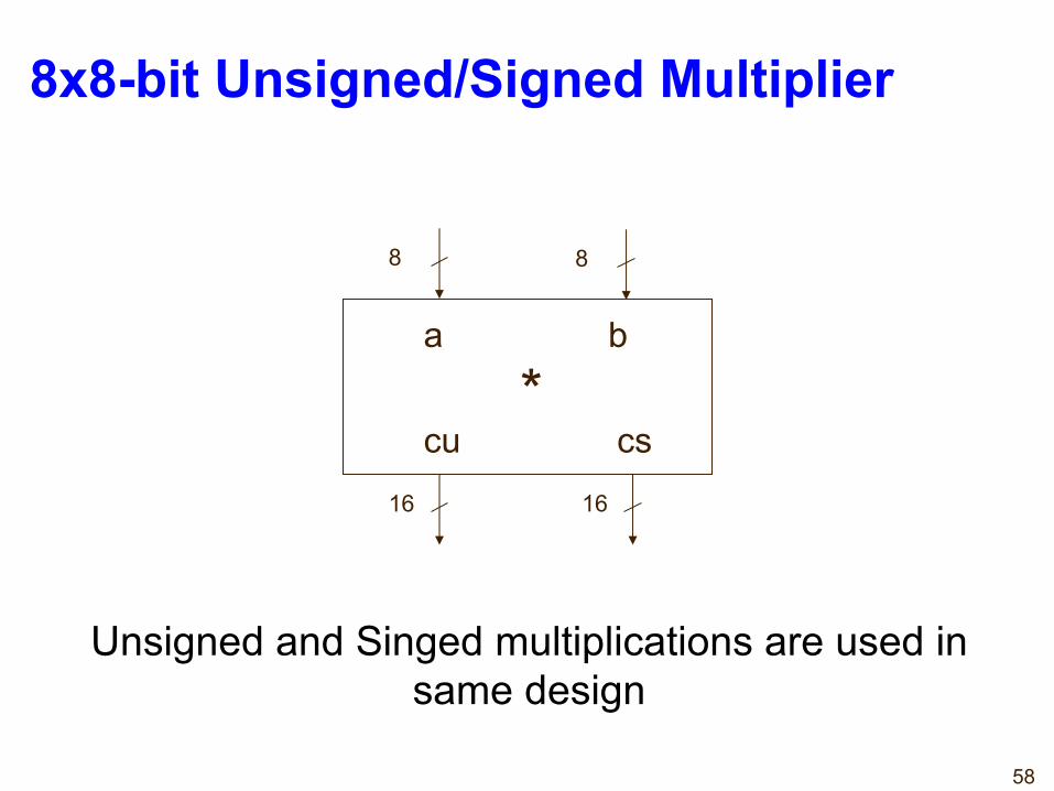
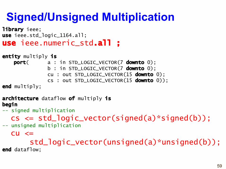
8x8-bit Unsigned/Signed Multiplier
8 8
a b
16
cu16
cs*
Unsigned and Singed multiplications are used in same design
59
Signed/Unsigned Multiplication library ieee;use ieee.std_logic_1164.all;
use ieee.numeric_std.all ;
entity multiply isport( a : in STD_LOGIC_VECTOR(7 downto 0);
b : in STD_LOGIC_VECTOR(7 downto 0);cu : out STD_LOGIC_VECTOR(15 downto 0); cs : out STD_LOGIC_VECTOR(15 downto 0));
end multiply;
architecture dataflow of multiply isbegin-- signed multiplication
cs <= std_logic_vector(signed(a)*signed(b));-- unsigned multiplication
cu <= std_logic_vector(unsigned(a)*unsigned(b));
end dataflow;
60
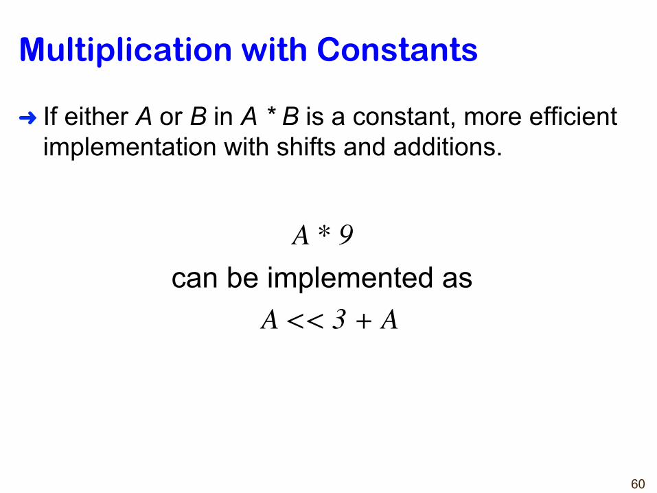
Multiplication with Constants
➜ If either A or B in A * B is a constant, more efficient implementation with shifts and additions.
A * 9 can be implemented as
A << 3 + A
61
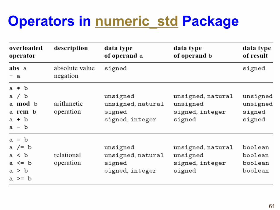
Operators in numeric_std Package
RTL Hardware Design by P. Chu
Chapter 3 47
Overloaded operators in IEEE numeric_std package
62
Parameterized Models
63
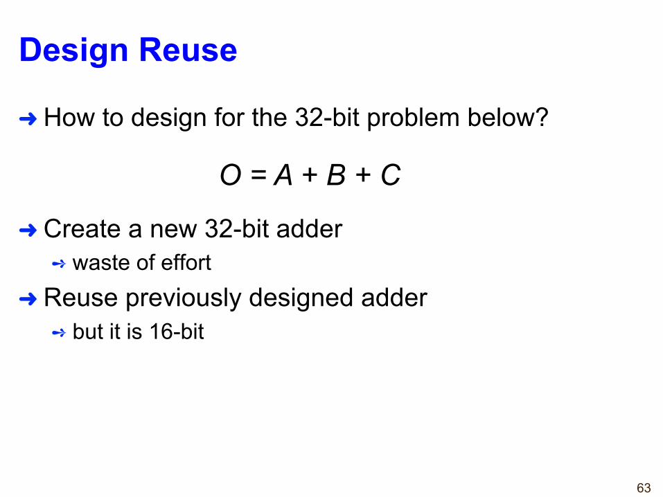
Design Reuse
➜ How to design for the 32-bit problem below?
➜ Create a new 32-bit adder➺ waste of effort
➜ Reuse previously designed adder➺ but it is 16-bit
O = A + B + C
64
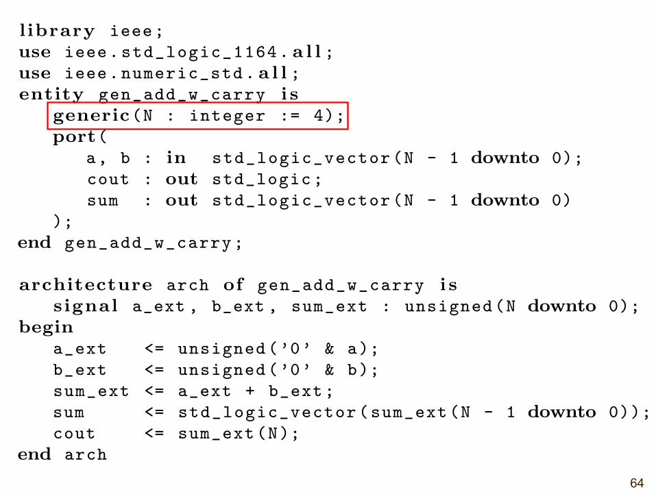
CONSTANTS AND GENERICS 43
3.5.2 Generics
VHDL provides a construct, known as a generic, to pass information into an entityand component. Since a generic cannot be modified inside the architecture, it func-tions somewhat like a constant. A generic is declared inside an entity declaration,just before the port declaration:
entity entity_name i sgeneric(
generic_name: data_type := default_value;generic_name: data_type := default_value;. . .generic_name: data_type := default_value
)port(
port_name: mode data_type;. . .
);end entity_name;
For example, the previous adder code can be modified to use the adder width as ageneric, as shown in Listing 3.11.
Listing 3.11 Adder using a generic
l ibrary ieee;use ieee.std_logic_1164. a l l ;use ieee.numeric_std. a l l ;entity gen_add_w_carry i s
generic(N : integer := 4);port(
a, b : in std_logic_vector(N - 1 downto 0);cout : out std_logic;sum : out std_logic_vector(N - 1 downto 0)
);end gen_add_w_carry;
architecture arch of gen_add_w_carry i ssignal a_ext , b_ext , sum_ext : unsigned(N downto 0);
begina_ext <= unsigned(’0’ & a);b_ext <= unsigned(’0’ & b);sum_ext <= a_ext + b_ext;sum <= std_logic_vector(sum_ext(N - 1 downto 0));cout <= sum_ext(N);
end arch
The N generic is declared in line 5 with a default value of 4. After N is declared, itcan be used in the port declaration and architecture body, just like a constant.
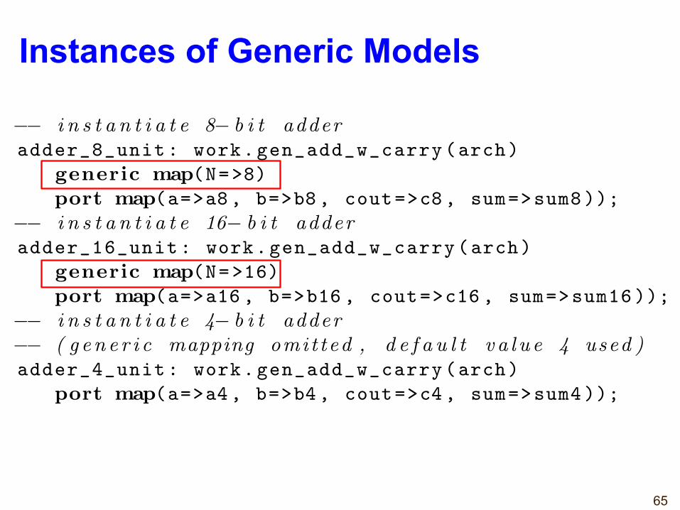
If the adder is later used as a component in other code, we can assign the desiredvalue to the generic in component instantiation. This is known as generic mapping .The default value will be used if generic mapping is omitted. Use of the generic incomponent instantiation is shown below.
s ignal a4, b4, sum4 : unsigned (3 downto 0);s ignal a8, b8, sum8 : unsigned (7 downto 0);s ignal a16 , b16 , sum16: unsigned (15 downto 0);s ignal c4, c8, c16 : std_logic;
Chu, Pong P.. FPGA Prototyping by VHDL Examples : Xilinx MicroBlaze MCS SoC, John Wiley & Sons, Incorporated, 2017. ProQuest Ebook Central, http://ebookcentral.proquest.com/lib/usf/detail.action?docID=5106967.Created from usf on 2018-05-09 06:53:33.
Cop
yrig
ht ©
201
7. J
ohn
Wile
y &
Sons
, Inc
orpo
rate
d. A
ll rig
hts
rese
rved
.
65
44 RT-LEVEL COMBINATIONAL CIRCUIT
. . .−− i n s t a n t i a t e 8− b i t adderadder_8_unit: work.gen_add_w_carry(arch)
generic map(N=>8)port map(a=>a8, b=>b8 , cout=>c8 , sum=>sum8 ));
−− i n s t a n t i a t e 16− b i t adderadder_16_unit: work.gen_add_w_carry(arch)
generic map(N=>16)port map(a=>a16 , b=>b16 , cout=>c16 , sum=>sum16 ));
−− i n s t a n t i a t e 4− b i t adder−− ( g en e r i c mapping omit ted , d e f a u l t v a l u e 4 used )adder_4_unit: work.gen_add_w_carry(arch)
port map(a=>a4, b=>b4 , cout=>c4 , sum=>sum4 ));
A generic provides a mechanism to create scalable code, in which the “width” ofa circuit can be adjusted to meet a specific need. This makes code more portableand encourages design reuse.
3.6 REPLICATED STRUCTURE
Many digital circuits exhibit a well-patterned structure, such as a one-dimensionalcascading chain or a two-dimensional mesh, and can be implemented as a repetitivecomposition of basic building blocks.
3.6.1 Loop statements
A replicated structure can be described by the VHDL for-generate and for-loopstatements. The former is a concurrent statement and the latter is a sequentialstatement.
The simplified syntax of the for-generate statement is
gen_label:for loop_index in loop_range generate
concurrent statement;concurrent statement;. . .
end generate;
The for-generate statement repeats the loop body of concurrent statements fora fixed number of iterations. The loop range term specifies a range of valuesbetween the left and right bounds. The range has to be static, which means thatit has to be determined before the time of execution (synthesis). It is normallyspecified by the width parameters. The loop index term is used to keep trackof the iteration and takes a successive value from loop range in each iteration,starting from the leftmost value. The index automatically takes the data type ofloop range’s element and does not need to be declared. The loop body contains acollection of concurrent statements and represents a stage of the iterative circuit.During synthesis, the loop is “unrolled” and flattened. The for-generate statementis frequently used in conjunction with generics to create scalable and reusable codes.
The for-loop statement is similar to the for-generate statement but is a sequentialstatement and can only be used within a process. The simplified syntax of the for-loop statement is
Chu, Pong P.. FPGA Prototyping by VHDL Examples : Xilinx MicroBlaze MCS SoC, John Wiley & Sons, Incorporated, 2017. ProQuest Ebook Central, http://ebookcentral.proquest.com/lib/usf/detail.action?docID=5106967.Created from usf on 2018-05-09 06:53:33.
Cop
yrig
ht ©
201
7. J
ohn
Wile
y &
Sons
, Inc
orpo
rate
d. A
ll rig
hts
rese
rved
.
Instances of Generic Models
66
Comparators
67
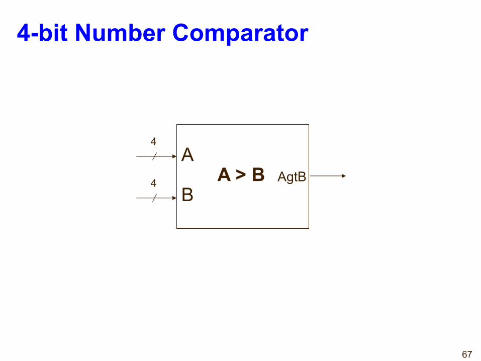
4-bit Number Comparator
4
4
A
BAgtBA > B
68
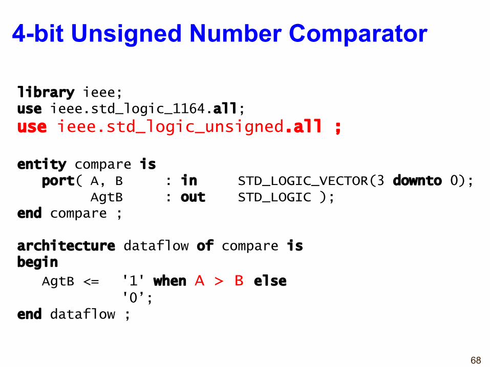
4-bit Unsigned Number Comparator
library ieee;use ieee.std_logic_1164.all;
use ieee.std_logic_unsigned.all ;
entity compare isport( A, B : in STD_LOGIC_VECTOR(3 downto 0);
AgtB : out STD_LOGIC );end compare ;
architecture dataflow of compare isbegin
AgtB <= '1' when A > B else
'0’;end dataflow ;
69
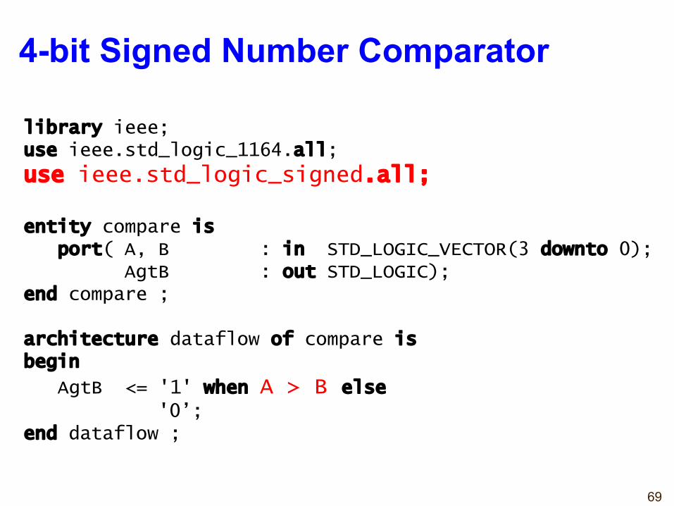
4-bit Signed Number Comparator
library ieee;use ieee.std_logic_1164.all;
use ieee.std_logic_signed.all;
entity compare isport( A, B : in STD_LOGIC_VECTOR(3 downto 0);
AgtB : out STD_LOGIC);end compare ;
architecture dataflow of compare isbegin
AgtB <= '1' when A > B else '0’;
end dataflow ;

70
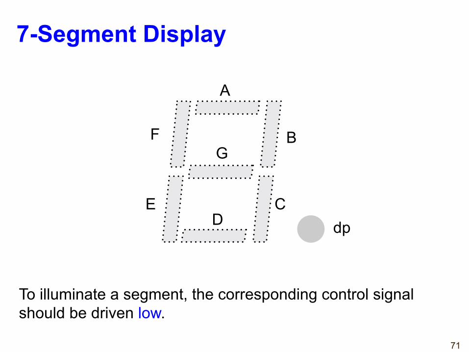
Hexadecimal to 7-Segment Display
71
7-Segment DisplayBasys3™ FPGA Board Reference Manual
Figure 17. An un-illuminated seven-segment display and nine illumination patterns corresponding to decimal digits.
The anodes of the seven LEDs forming each digit are tied together into one “common anode” circuit node, but the LED cathodes remain separate, as shown in Fig. 18. The common anode signals are available as four “digit enable” input signals to the 4-digit display. The cathodes of similar segments on all four displays are connected into seven circuit nodes labeled CA through CG (for example, the four “D” cathodes from the four digits are grouped together into a single circuit node called “CD”). These seven cathode signals are available as inputs to the 4-digit display. This signal connection scheme creates a multiplexed display, where the cathode signals are common to all digits but they can only illuminate the segments of the digit whose corresponding anode signal is asserted.
To illuminate a segment, the anode should be driven high while the cathode is driven low. However, since the Basys3 uses transistors to drive enough current into the common anode point, the anode enables are inverted. Therefore, both the AN0..3 and the CA..G/DP signals are driven low when active.
AF
E
D
C
B
G
Common anode
Individual cathodes
DP
AN3 AN2 AN1 AN0
CA CB CC CD CE CF CG DP
Four-digit Seven Segment Display
Figure 18. Common anode circuit node.
A scanning display controller circuit can be used to show a four-digit number on this display. This circuit drives the anode signals and corresponding cathode patterns of each digit in a repeating, continuous succession at an update rate that is faster than the human eye can detect. Each digit is illuminated just one-fourth of the time, but because the eye cannot perceive the darkening of a digit before it is illuminated again, the digit appears continuously illuminated. If the update, or “refresh”, rate is slowed to around 45Hz, a flicker can be noticed in the display.
For each of the four digits to appear bright and continuously illuminated, all four digits should be driven once every 1 to 16ms, for a refresh frequency of about 1 KHz to 60Hz. For example, in a 62.5Hz refresh scheme, the entire display would be refreshed once every 16ms, and each digit would be illuminated for 1/4 of the refresh cycle, or 4ms. The controller must drive the cathodes low with the correct pattern when the corresponding anode signal is driven high. To illustrate the process, if AN0 is asserted while CB and CC are asserted, then a “1” will be displayed
Copyright Digilent, Inc. All rights reserved. Other product and company names mentioned may be trademarks of their respective owners. Page 16 of 19
A
F
ED
C
BG
dp
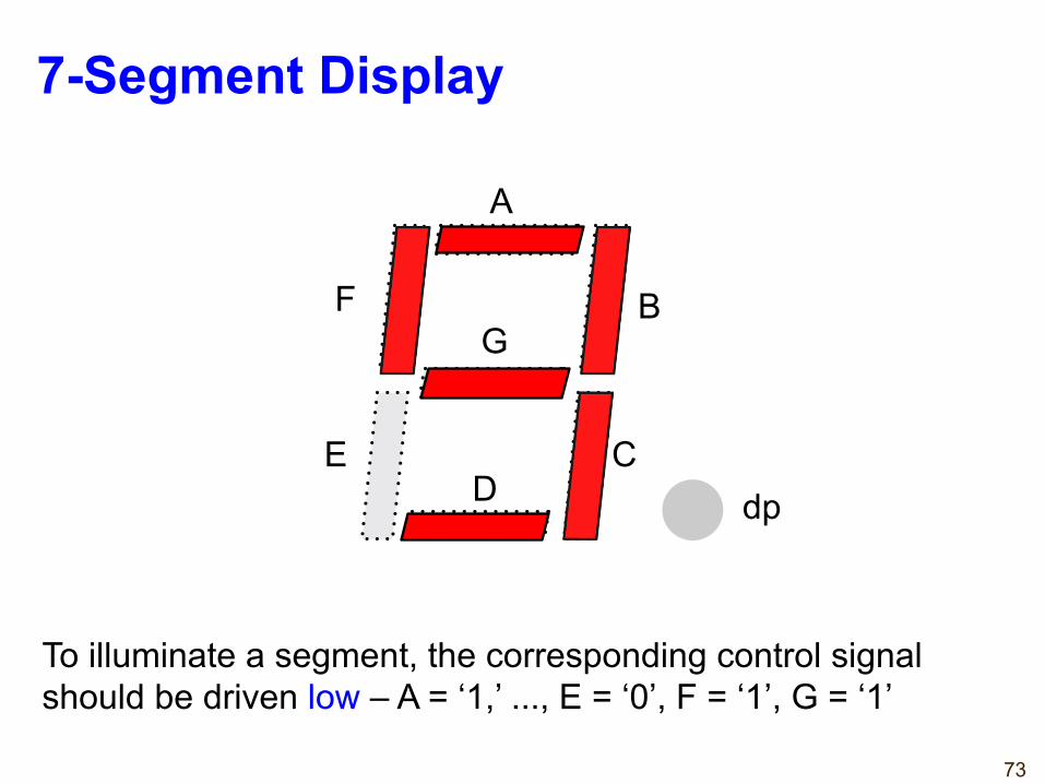
To illuminate a segment, the corresponding control signal should be driven low.
72
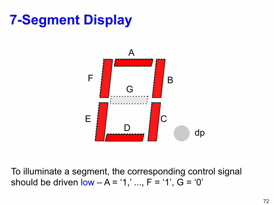
7-Segment DisplayBasys3™ FPGA Board Reference Manual
Figure 17. An un-illuminated seven-segment display and nine illumination patterns corresponding to decimal digits.
The anodes of the seven LEDs forming each digit are tied together into one “common anode” circuit node, but the LED cathodes remain separate, as shown in Fig. 18. The common anode signals are available as four “digit enable” input signals to the 4-digit display. The cathodes of similar segments on all four displays are connected into seven circuit nodes labeled CA through CG (for example, the four “D” cathodes from the four digits are grouped together into a single circuit node called “CD”). These seven cathode signals are available as inputs to the 4-digit display. This signal connection scheme creates a multiplexed display, where the cathode signals are common to all digits but they can only illuminate the segments of the digit whose corresponding anode signal is asserted.
To illuminate a segment, the anode should be driven high while the cathode is driven low. However, since the Basys3 uses transistors to drive enough current into the common anode point, the anode enables are inverted. Therefore, both the AN0..3 and the CA..G/DP signals are driven low when active.
AF
E
D
C
B
G
Common anode
Individual cathodes
DP
AN3 AN2 AN1 AN0
CA CB CC CD CE CF CG DP
Four-digit Seven Segment Display
Figure 18. Common anode circuit node.
A scanning display controller circuit can be used to show a four-digit number on this display. This circuit drives the anode signals and corresponding cathode patterns of each digit in a repeating, continuous succession at an update rate that is faster than the human eye can detect. Each digit is illuminated just one-fourth of the time, but because the eye cannot perceive the darkening of a digit before it is illuminated again, the digit appears continuously illuminated. If the update, or “refresh”, rate is slowed to around 45Hz, a flicker can be noticed in the display.
For each of the four digits to appear bright and continuously illuminated, all four digits should be driven once every 1 to 16ms, for a refresh frequency of about 1 KHz to 60Hz. For example, in a 62.5Hz refresh scheme, the entire display would be refreshed once every 16ms, and each digit would be illuminated for 1/4 of the refresh cycle, or 4ms. The controller must drive the cathodes low with the correct pattern when the corresponding anode signal is driven high. To illustrate the process, if AN0 is asserted while CB and CC are asserted, then a “1” will be displayed
Copyright Digilent, Inc. All rights reserved. Other product and company names mentioned may be trademarks of their respective owners. Page 16 of 19
A
F
ED
C
BG
dp
To illuminate a segment, the corresponding control signal should be driven low – A = ‘1,’ ..., F = ‘1’, G = ‘0’
73
7-Segment DisplayBasys3™ FPGA Board Reference Manual
Figure 17. An un-illuminated seven-segment display and nine illumination patterns corresponding to decimal digits.
The anodes of the seven LEDs forming each digit are tied together into one “common anode” circuit node, but the LED cathodes remain separate, as shown in Fig. 18. The common anode signals are available as four “digit enable” input signals to the 4-digit display. The cathodes of similar segments on all four displays are connected into seven circuit nodes labeled CA through CG (for example, the four “D” cathodes from the four digits are grouped together into a single circuit node called “CD”). These seven cathode signals are available as inputs to the 4-digit display. This signal connection scheme creates a multiplexed display, where the cathode signals are common to all digits but they can only illuminate the segments of the digit whose corresponding anode signal is asserted.
To illuminate a segment, the anode should be driven high while the cathode is driven low. However, since the Basys3 uses transistors to drive enough current into the common anode point, the anode enables are inverted. Therefore, both the AN0..3 and the CA..G/DP signals are driven low when active.
AF
E
D
C
B
G
Common anode
Individual cathodes
DP
AN3 AN2 AN1 AN0
CA CB CC CD CE CF CG DP
Four-digit Seven Segment Display
Figure 18. Common anode circuit node.
A scanning display controller circuit can be used to show a four-digit number on this display. This circuit drives the anode signals and corresponding cathode patterns of each digit in a repeating, continuous succession at an update rate that is faster than the human eye can detect. Each digit is illuminated just one-fourth of the time, but because the eye cannot perceive the darkening of a digit before it is illuminated again, the digit appears continuously illuminated. If the update, or “refresh”, rate is slowed to around 45Hz, a flicker can be noticed in the display.
For each of the four digits to appear bright and continuously illuminated, all four digits should be driven once every 1 to 16ms, for a refresh frequency of about 1 KHz to 60Hz. For example, in a 62.5Hz refresh scheme, the entire display would be refreshed once every 16ms, and each digit would be illuminated for 1/4 of the refresh cycle, or 4ms. The controller must drive the cathodes low with the correct pattern when the corresponding anode signal is driven high. To illustrate the process, if AN0 is asserted while CB and CC are asserted, then a “1” will be displayed
Copyright Digilent, Inc. All rights reserved. Other product and company names mentioned may be trademarks of their respective owners. Page 16 of 19
A
F
ED
C
BG
dp
To illuminate a segment, the corresponding control signal should be driven low – A = ‘1,’ ..., E = ‘0’, F = ‘1’, G = ‘1’
74
Hex to 7-SegmentHex Input 7-Segment Control
GFE...BCA
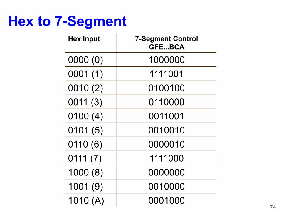
0000 (0) 10000000001 (1) 11110010010 (2) 01001000011 (3) 01100000100 (4) 00110010101 (5) 00100100110 (6) 00000100111 (7) 11110001000 (8) 00000001001 (9) 00100001010 (A) 0001000
75
7-Segment Display
Basys3™ FPGA Board Reference Manual
Figure 17. An un-illuminated seven-segment display and nine illumination patterns corresponding to decimal digits.
The anodes of the seven LEDs forming each digit are tied together into one “common anode” circuit node, but the LED cathodes remain separate, as shown in Fig. 18. The common anode signals are available as four “digit enable” input signals to the 4-digit display. The cathodes of similar segments on all four displays are connected into seven circuit nodes labeled CA through CG (for example, the four “D” cathodes from the four digits are grouped together into a single circuit node called “CD”). These seven cathode signals are available as inputs to the 4-digit display. This signal connection scheme creates a multiplexed display, where the cathode signals are common to all digits but they can only illuminate the segments of the digit whose corresponding anode signal is asserted.
To illuminate a segment, the anode should be driven high while the cathode is driven low. However, since the Basys3 uses transistors to drive enough current into the common anode point, the anode enables are inverted. Therefore, both the AN0..3 and the CA..G/DP signals are driven low when active.
AF
E
D
C
B
G
Common anode
Individual cathodes
DP
AN3 AN2 AN1 AN0
CA CB CC CD CE CF CG DP
Four-digit Seven Segment Display
Figure 18. Common anode circuit node.
A scanning display controller circuit can be used to show a four-digit number on this display. This circuit drives the anode signals and corresponding cathode patterns of each digit in a repeating, continuous succession at an update rate that is faster than the human eye can detect. Each digit is illuminated just one-fourth of the time, but because the eye cannot perceive the darkening of a digit before it is illuminated again, the digit appears continuously illuminated. If the update, or “refresh”, rate is slowed to around 45Hz, a flicker can be noticed in the display.
For each of the four digits to appear bright and continuously illuminated, all four digits should be driven once every 1 to 16ms, for a refresh frequency of about 1 KHz to 60Hz. For example, in a 62.5Hz refresh scheme, the entire display would be refreshed once every 16ms, and each digit would be illuminated for 1/4 of the refresh cycle, or 4ms. The controller must drive the cathodes low with the correct pattern when the corresponding anode signal is driven high. To illustrate the process, if AN0 is asserted while CB and CC are asserted, then a “1” will be displayed
Copyright Digilent, Inc. All rights reserved. Other product and company names mentioned may be trademarks of their respective owners. Page 16 of 19
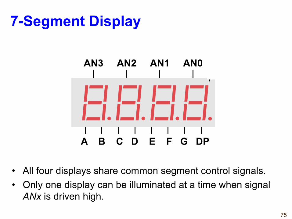
• All four displays share common segment control signals.• Only one display can be illuminated at a time when signal
ANx is driven high.
A B C D E F G DP
76
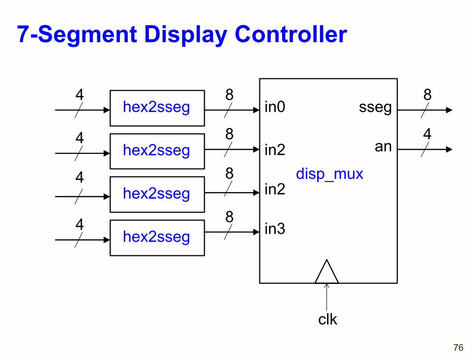
7-Segment Display Controller
disp_mux
8
8
8
8
in0
in2
in2
in3
sseg
an
8
4
hex2sseg4
hex2sseg4
hex2sseg4
hex2sseg4
clk
77
Binary to BCD Conversion
78
for(i=0; i<8; i++) {
// add 3 to a column if it is >= 5
for each column
if (column >= 5)
column += 3;
// shift binary digits left 1
Hundred << 1;
Hundreds[0] = Tens[3];
Tens << 1;
Tens[3] = Ones[3];
Ones << 1;
Ones = Binary[7];
Binary << 1;
}
Shift and Add-3 (Double-Dabble)
79
1. If the binary value in any of the BCD columns is 5 or greater, add 3 to that value in that BCD column.
2. Shift the binary number left one bit. 3. If 8 shifts have taken place, the BCD number is in the
Hundreds, Tens, and Ones column. Terminate4. Otherwise, go to 1.
Example:
Hundreds Tens Ones Binary
0000 0000 0000 11110011
Shift and Add-3 (Double-Dabble)
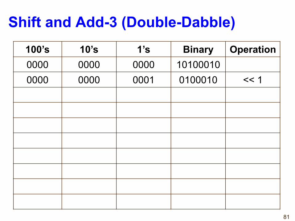
80
100’s 10’s 1’s Binary Operation0000 0000 0000 10100010
Shift and Add-3 (Double-Dabble)
81
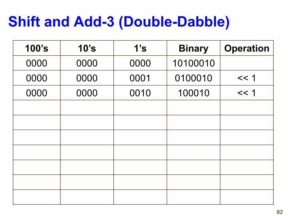
100’s 10’s 1’s Binary Operation0000 0000 0000 101000100000 0000 0001 0100010 << 1
Shift and Add-3 (Double-Dabble)
82
100’s 10’s 1’s Binary Operation0000 0000 0000 101000100000 0000 0001 0100010 << 10000 0000 0010 100010 << 1
Shift and Add-3 (Double-Dabble)
83
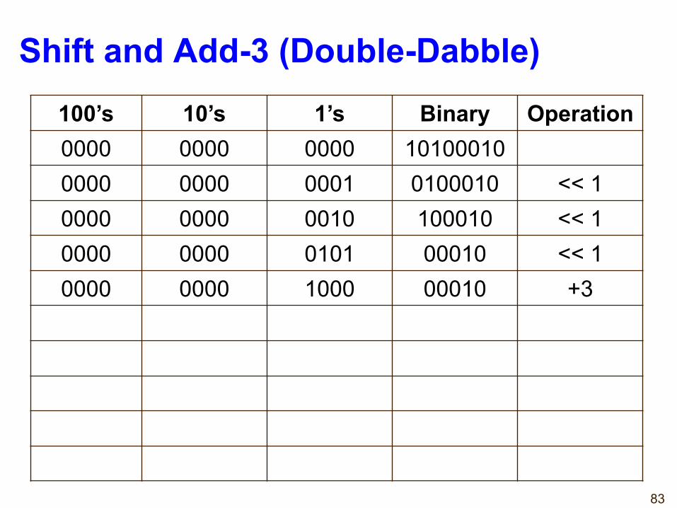
100’s 10’s 1’s Binary Operation0000 0000 0000 101000100000 0000 0001 0100010 << 10000 0000 0010 100010 << 10000 0000 0101 00010 << 10000 0000 1000 00010 +3
Shift and Add-3 (Double-Dabble)
84
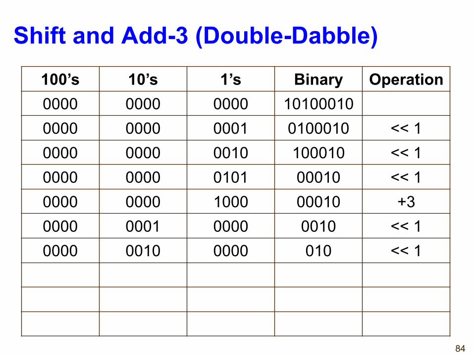
100’s 10’s 1’s Binary Operation0000 0000 0000 101000100000 0000 0001 0100010 << 10000 0000 0010 100010 << 10000 0000 0101 00010 << 10000 0000 1000 00010 +30000 0001 0000 0010 << 10000 0010 0000 010 << 1
Shift and Add-3 (Double-Dabble)
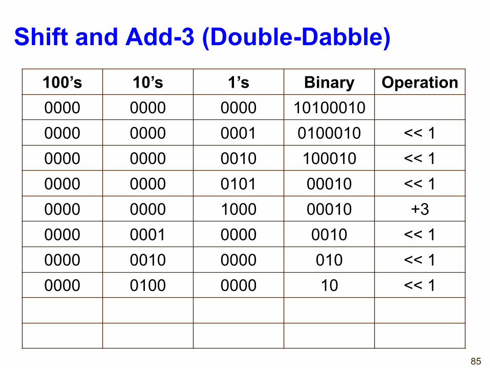
85
100’s 10’s 1’s Binary Operation0000 0000 0000 101000100000 0000 0001 0100010 << 10000 0000 0010 100010 << 10000 0000 0101 00010 << 10000 0000 1000 00010 +30000 0001 0000 0010 << 10000 0010 0000 010 << 10000 0100 0000 10 << 1
Shift and Add-3 (Double-Dabble)
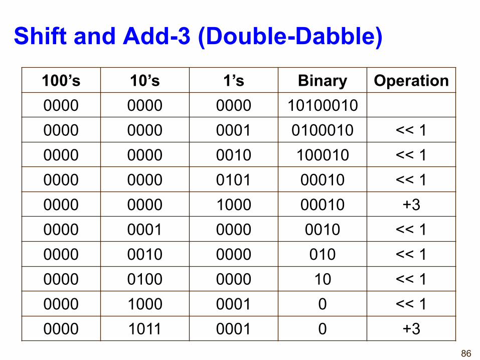
86
100’s 10’s 1’s Binary Operation0000 0000 0000 101000100000 0000 0001 0100010 << 10000 0000 0010 100010 << 10000 0000 0101 00010 << 10000 0000 1000 00010 +30000 0001 0000 0010 << 10000 0010 0000 010 << 10000 0100 0000 10 << 10000 1000 0001 0 << 10000 1011 0001 0 +3
Shift and Add-3 (Double-Dabble)
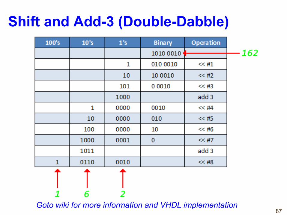
87Goto wiki for more information and VHDL implementation
Shift and Add-3 (Double-Dabble)

88
Backup
89
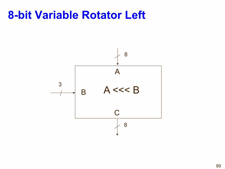
8-bit Variable Rotator Left
8
8
3
A
B
C
A <<< B
90
Tri-State Buffers
91
(b) Equivalent circuit
(c) Truth table
x f
e
(a) A tri-state buffer
0 0 1 1
0 1 0 1
Z Z 0 1
f e x
x f
e = 0
e = 1x f
Tri-State Buffers
92
x f
e
(b)
x f
e
(a)
x f
e
(c)
x f
e
(d)
Four types of Tri-state Buffers
93
Tri-state Buffer – Example (1)
LIBRARY ieee;
USE ieee.std_logic_1164.all;
entity tri_state is
port( ena, input : IN STD_LOGIC;
output : OUT STD_LOGIC);
end tri_state;
architecture dataflow of tri_state is
begin
output <= input when (ena = ‘1’) else
‘Z’;end dataflow;

94
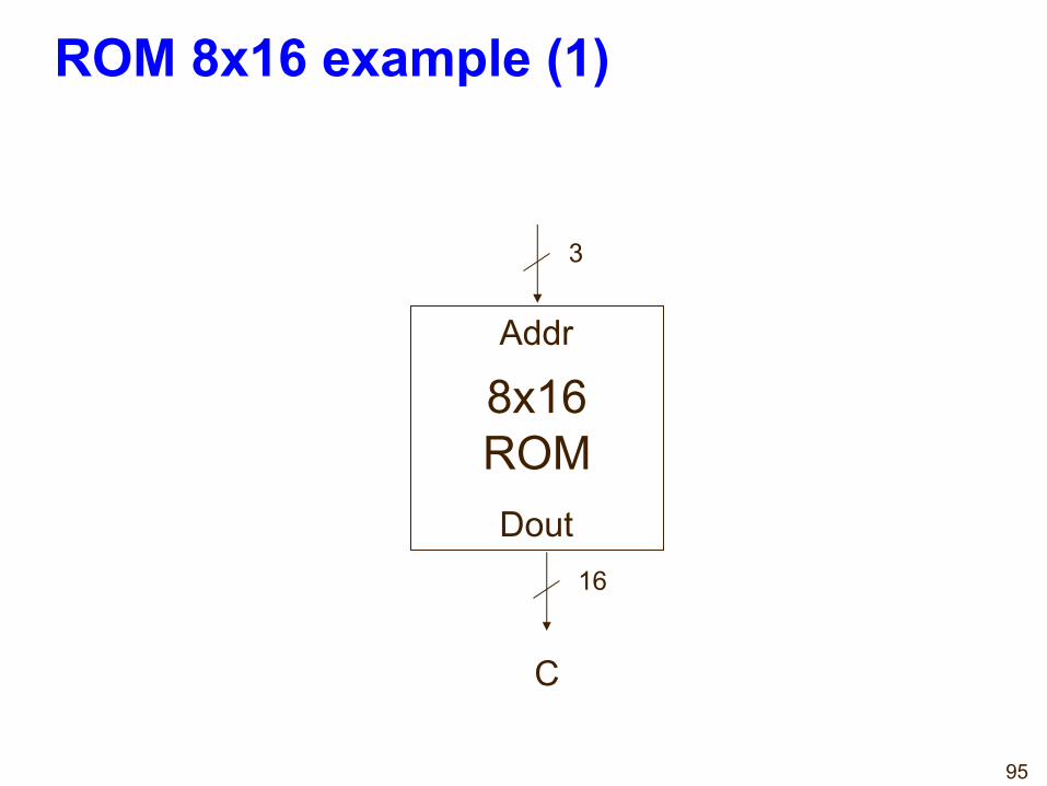
ROM
95
3
16
Addr
C
8x16ROMDout
ROM 8x16 example (1)
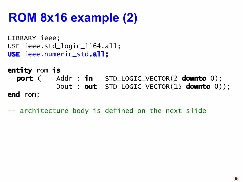
96
ROM 8x16 example (2)LIBRARY ieee;USE ieee.std_logic_1164.all;USE ieee.numeric_std.all;
entity rom isport ( Addr : in STD_LOGIC_VECTOR(2 downto 0);
Dout : out STD_LOGIC_VECTOR(15 downto 0));end rom;
-- architecture body is defined on the next slide
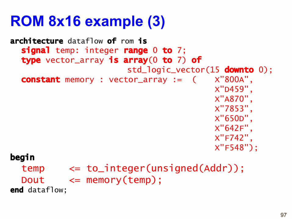
97
architecture dataflow of rom is
signal temp: integer range 0 to 7;type vector_array is array(0 to 7) of
std_logic_vector(15 downto 0);constant memory : vector_array := ( X”800A",
X"D459",X"A870",X"7853",X"650D",X"642F",X"F742",X"F548");
begin
temp <= to_integer(unsigned(Addr));Dout <= memory(temp);
end dataflow;
ROM 8x16 example (3)