Embed Size (px)
Citation preview
CdSe Colloidal Quantum Rings
Sébastien A. Lamarre,†,‡ Étienne Rochette,†,‡ Samuel Tremblay,¶,‡ and ClaudineNì. Allen∗,¶,‡
Département de chimie, Université Laval, Québec, G1V 0A6, Canada, Centre d’optique,photonique et laser (COPL), and Département de physique, de génie physique et d’optique,
Université Laval, Québec, G1V 0A6, Canada
E-mail: [email protected]
AbstractAtomically flat semiconductor nanostructures havesharp photoluminescence emission, short radiativelifetimes and a well-defined planar structure. How-ever, these nanostructures lack the optical and elec-tronic fine-tuning that justify extensive researchin colloidal quantum dots. Here, we propose aheterostructure based on CdS nanoplatelets withlaterally grown CdSe. Samples of two differentthickness and varying ring width are synthesizedby a one-pot method during which CdSe ring widthis controlled by Se precursor amount. The CdSe di-mensionality is continuously tuned from a 0D arrayof CdSe dots to a 1D CdSe quantum ring and finallya 2D CdSe nanoplatelet. Sample characterizationshows that their optical properties are tunable byboth structure thickness and CdSe ring width. Thiscontinuous tunability extends the emission rangeof nanoplatelet-based structures from 428 nm to512 nm for 3 and 4 monolayers structures.
IntroductionMesoscale rings were the object of numerous ex-
periments exploring quantum mechanical phenom-ena involving phase shifts and coherence of elec-
∗To whom correspondence should be addressed†Département de chimie, Université Laval, Québec, G1V
0A6, Canada‡Centre d’optique, photonique et laser (COPL)¶Département de physique, de génie physique et
d’optique, Université Laval, Québec, G1V 0A6, Canada
tronic wavefunctions. Among others, persistent cur-rents,1,2 one-dimensional weak localization3 andthe Aharonov-Bohm effect4 were studied. Theserings have been fabricated using various materi-als: superconductors,5 metals,6 semiconductors,7
two-dimensional free electron gas systems,8 carbonnanotubes3 and graphene.9 As an example applica-tion for these structures, Suarez et al. used epitaxialquantum rings (QRs) as gain medium for lasers.10
Until recently, these structures were not availablein colloidal form. Since 2008, freestanding quan-tum wells called nanoplatelets (NPLs), nanodisksor nanobelts are accessible using colloidal syn-thesis, enabling a larger and cheaper source ofquantum wells. Many colloidal II-VI semicon-ductor nanoplatelets having a well-defined modula-ble thickness and atomically flat surface have beendirectly prepared by solution phase methods, e.g.CdS,11–13 CdSe,13–17 CdSxSe1-x,18 CdTe13,19–21
and ZnS.22 Cation exchange methods also allowedthe preparation of ZnSe and PbSe NPLs.23
As the NPL growth originates from the directreaction of precursor at the NPL periphery,24 itis possible to grow another semiconductor later-ally around a NPL acting as a seed. One suchheterostructure, CdSe/CdS core/crown, has beensynthesized by Prudnikau et al.25 and Tessier etal.26 Also, CdSe/CdTe core/crown have been pre-pared by Pedetti et al.27 and Kelestemur et al.28
These former structures show good confinementbecause of rapid exciton transfer from the CdScrown to the CdSe core. However, their emission
1
arX
iv:1
509.
0779
3v2
[co
nd-m
at.m
trl-
sci]
28
Sep
2015
is mostly dependent on the core dimensions andis not easily modulated.26 To extend the emissionwindow of NPL based heterostructures, we proposeCdSe colloidal QRs, thereafter cQRs, grown at theperiphery of CdS NPLs. As expected from theband alignment, the emission of these heterostruc-tures originates from the excitonic recombinationin the CdSe QR. Such colloidal quantum rings haverecently been reported in parallel by Delikanli etal.29 but prepared by a different method and onlywith 4 monolayers (ML) thick CdS seed. In com-parison, the presented method is a user-friendlyone-pot synthesis and was used to prepared both3 and 4 ML heterostructures. Colloidal QRs, astheir core/crown analog, could be used in light har-vesting and charge separator for solar cells, activemedium for laser30 and light-emitting diode,31 andeven luminescent probe for biomedical imaging.Furthermore, the peculiar electronic structure ofQRs has an importance for more fundamental phys-ical studies4,8,32,33 and light matter interaction.34,35
Here, we present the synthesis and character-ization of CdSe colloidal QRs grown around 3and 4 monolayers. The samples are characterizedby elemental analysis, X-ray diffraction, transmis-sion electron microscopy, absorption, photolumi-nescence emission and photoluminescence excita-tion spectroscopy. We describe the evolution of theCdSe dimensionality with the width of the CdSeQR from 0D to 2D with an intermediate 1D state.
Experimental MethodsChemicals Cadmium acetate dihydrate(Cd(Ac)2 ·2 H2O, 98 %), technical grade 1-octadecene (ODE, 90 %) and technical grade tri-n-butylphosphine (TBP, 95 %) were purchased fromAlfa Aesar. Technical grade oleic acid (OA, 90 %)and elemental selenium (99.5 %) were purchasedfrom Sigma Aldrich. Chloroform and methanolwere purchased from BDH and elemental sulfur(99 %) from Laboratoire Mat. All chemicals wereused as purchased without further purification.
Preparation of stock solutions Sulfur stock so-lution was prepared by dissolving 32 mg of elemen-tal sulfur in 20 g of ODE by sonication at room tem-
perature. 0.1 M Se stock solution was prepared byheating, under inert atmosphere, 318 mg of elemen-tal selenium in 40 mL of ODE at 180 ◦C overnight.The resulting solution was yellow and was con-served under ambient conditions.
4 ML CdS nanoplatelet synthesis In a 250 mLreaction flask, 2 mmol of cadmium acetate, 10 gof S stock solution, 2 mmol of OA and 30 g ofODE were degassed under vacuum at 50 ◦C for30 min and purged twice with nitrogen. The mix-ture was then heated under nitrogen to 260 ◦C inabout 15 min. The mixture reacted at this tempera-ture, but not above, for 1 min before being cooleddown to ambient temperature. At the beginning ofthe cooldown, 3 mL of OA was added to improvethe purification process and the stability of the puri-fied nanoplatelets. After the cooldown, the mixturewas centrifuged at 6000 rcf for 6 min and the pre-cipitated nanoplatelets were redispersed in 20 mLof chloroform.
3 ML CdS nanoplatelet synthesis 3 ML CdSnanoplatelets were prepared in a similar manner.Instead of oleic acid, the same molar amount ofmyristic acid was used for the reaction mixture.For this synthesis, the reaction time and tempera-ture were 20 min and 180 ◦C.
CdSe ring synthesis around CdS nanoplateletsIn a typical synthesis for cQRs, 0.1 mmol of cad-mium acetate, 15 mg of oleic acid, 0.5 mL of a CdSNPL dispersion, 0.5 mL of the Se stock solutionand 15 mL of ODE were added to a 100 mL reac-tion flask, degassed at 50 ◦C and purged twice withnitrogen. The mixture was heated to 190 ◦C andkept at this temperature, never above, for 10 min.Afterward, 1 mL of oleic acid was injected and themixture was cooled to room temperature. The mix-ture was centrifuged at 11000 rcf for 8 min. Theprecipitated cQRs were redispersed in 6 mL of chlo-roform. The dispersions are colloidally stable formonths.
The ring width is controlled by the amount ofSe added. This amount can be lowered down to5 µmol to obtain a narrower ring. Above 50 µmol,the concentration of selenium was too high and
2
secondary CdSe NPL and dot nucleation hinderedring growth. To obtain the sample with more than50 µmol of Se, cQRs with 50 µmol of Se were pre-pared according to the method. After the 10 minreaction time, the remaining Se quantity, up to anadditional 50 µmol was injected in the reactionflask and the temperature was kept at 190 ◦C for10 more minutes. Multiples injections were usedfor samples above 100 µmol of Se.
Energy-dispersive X-ray spectroscopy (EDS)EDS measurements were obtained with a JEOLJSM-840-A scanning electron microscope usinga PGT Avalon EDS with a NORA detecting unit.The samples were scanned with a 15 kV electronbeam.
Powder X-ray Diffraction (XRD) Diffrac-tograms were acquired using a Siemens-BrukerX-ray diffractometer with a 2D Hi-Star XRD de-tector. The radiation source was a Kristalloflex760 with a nickel window emitting the Cu Kα
line (λ = 1.5418Å) with an accelerating volt-age and current of respectively 40 kV and 40 mA.Diffractograms were recorded from 10◦ to 60◦.Background signal was automatically subtracted bythe diffraction pattern treatment software GADDS.
Purification method for EDS and XRD cQRdispersions were centrifuged at low force to elim-inate the remaining insoluble compounds. After-ward, the cQRs were precipitated in a solution of10 % TBP in methanol and centrifuged. The pre-cipitate was dispersed with chloroform. This pre-cipitation cycle was repeated once more with theTBP solution and once again with pure methanolas precipitating solvent. Finally, the cQRs wereredispersed in a minimal amount of chloroform anddrop-casted on a Si wafer for the EDS and on aglass cover slip for XRD analysis.
Transmission electron microscope (TEM) Thepurified cQR samples morphology was character-ized with a JEOL 1230. The samples dispersedin chloroform were drop-casted on a Ni TEM gridcoated with Formvar and carbon film.
Optical spectroscopy All optical characteriza-tions were carried out on cQR dispersions in chlo-roform. Absorption spectra of the samples wererecorded at room temperature with a Varian Cary50 Conc UV-visible spectrophometer from 300to 800 nm. The steady state photoluminescence(PL) and photoluminescence excitation (PLE) spec-tra were acquired using a Jobin-Yvon Fluorologequipped with a photomultiplicator tube. The sam-ples were excited at 350 nm for PL spectra and thedetection window was set at the emission maxi-mum for PLE spectra. Excitation and emissionmonochromators slits were set at 1 nm.
Photoluminescence peak fitting PL spectrawere fitted to extract their respective photolumi-nescence maximum energy (PLmax) and full widthhalf maximum (FWHM). Depending on the Seamount added during the cQR synthesis, the PLbehaviour might correspond to either a Gaussianor Lorentzian peak shape, which correspond todifferent broadening types, as discussed in Spec-troscopic Characterization section. Thus, all PLspectra were fitted with both peak shapes on an in-terval corresponding to the exitonic peak. Then, foreach spectrum, the most representative peak shapewas determined by comparing each fit’s coefficientof determination (R2) over the whole spectrum.From this best fit, the PLmax was directly obtainedfrom the fit’s center parameter and the FHWM wascalculated from the fit’s width parameter.
Results and Discussion
Synthesis and Expected Growth Mech-anism
The synthesis of these CdSe cQRs involves twosteps. First, CdS nanoplatelets of 3 ML and 4 MLare prepared following a one-pot method reportedby M. Li et al.12 and Z. Li et al.11 Compared to con-tinuous injection methods, this approach is moreeasily implemented for various experimental con-ditions and facilitates synthesis scale up. Second,the growth of a CdSe ring around the CdS NPLperiphery is also inspired from a CdSe NPL syn-thesis.17 The one-pot method presented has theadvantage of being more user-friendly than con-
3
tinuous injection method and yields reproducibleresults as all the results were replicated by anotheruser. As with CdSe NPL synthesis, the reactionconditions are critical for the growth of atomicallyflat CdSe. The range of synthetic temperatures isbelow the solubilization temperature of the CdSand CdSe NPLs and higher than the monomer re-action temperature/sout. The reaction temperaturehas to be higher than the monomer reaction temper-ature (140 ◦C).17 At higher temperatures (240 ◦C),the NPLs are not stable and the formation of irreg-ular free CdSe nanocrystals is more favorable thanlateral growth.17 The Se precursor concentration iskept low to promote heterogeneous nucleation andgrowth of CdSe around CdS NPLs over secondaryhomogeneous CdSe nucleation.
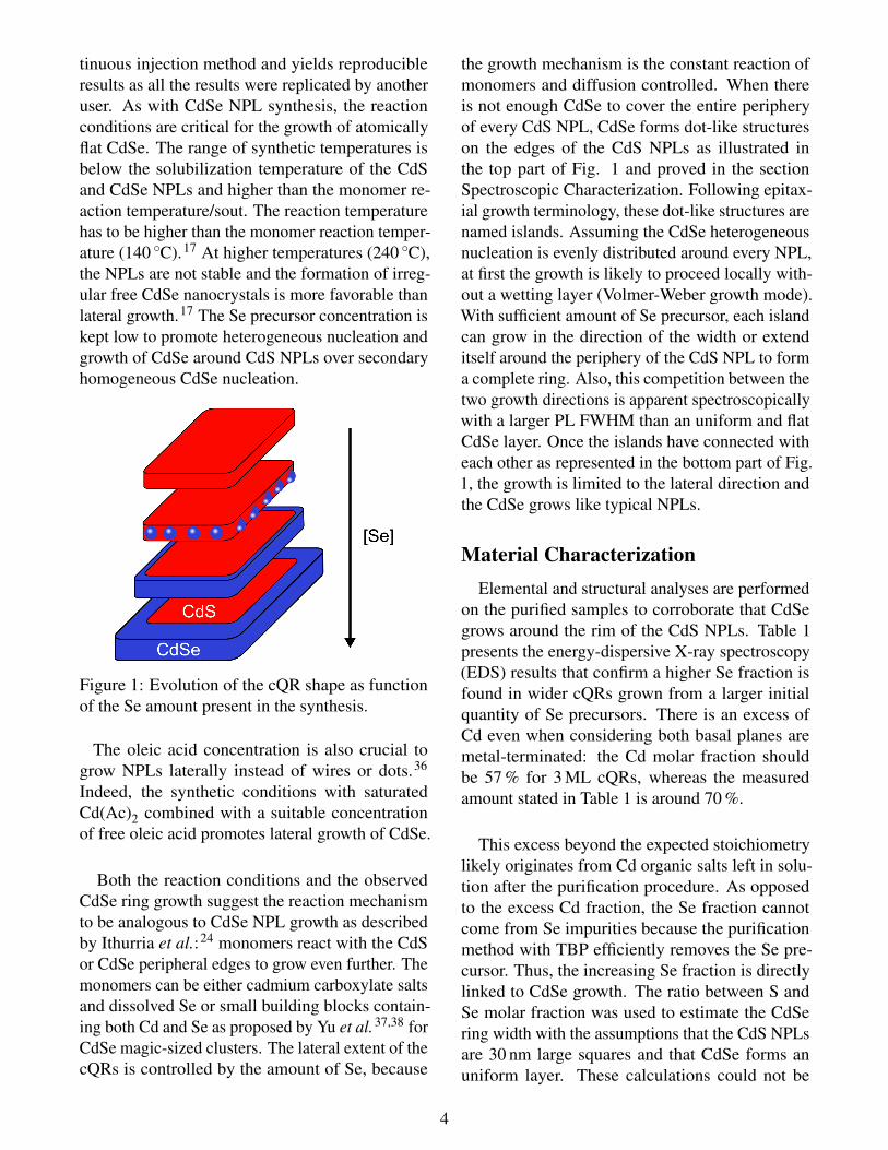
Figure 1: Evolution of the cQR shape as functionof the Se amount present in the synthesis.
The oleic acid concentration is also crucial togrow NPLs laterally instead of wires or dots.36
Indeed, the synthetic conditions with saturatedCd(Ac)2 combined with a suitable concentrationof free oleic acid promotes lateral growth of CdSe.
Both the reaction conditions and the observedCdSe ring growth suggest the reaction mechanismto be analogous to CdSe NPL growth as describedby Ithurria et al.:24 monomers react with the CdSor CdSe peripheral edges to grow even further. Themonomers can be either cadmium carboxylate saltsand dissolved Se or small building blocks contain-ing both Cd and Se as proposed by Yu et al.37,38 forCdSe magic-sized clusters. The lateral extent of thecQRs is controlled by the amount of Se, because
the growth mechanism is the constant reaction ofmonomers and diffusion controlled. When thereis not enough CdSe to cover the entire peripheryof every CdS NPL, CdSe forms dot-like structureson the edges of the CdS NPLs as illustrated inthe top part of Fig. 1 and proved in the sectionSpectroscopic Characterization. Following epitax-ial growth terminology, these dot-like structures arenamed islands. Assuming the CdSe heterogeneousnucleation is evenly distributed around every NPL,at first the growth is likely to proceed locally with-out a wetting layer (Volmer-Weber growth mode).With sufficient amount of Se precursor, each islandcan grow in the direction of the width or extenditself around the periphery of the CdS NPL to forma complete ring. Also, this competition between thetwo growth directions is apparent spectroscopicallywith a larger PL FWHM than an uniform and flatCdSe layer. Once the islands have connected witheach other as represented in the bottom part of Fig.1, the growth is limited to the lateral direction andthe CdSe grows like typical NPLs.
Material CharacterizationElemental and structural analyses are performed
on the purified samples to corroborate that CdSegrows around the rim of the CdS NPLs. Table 1presents the energy-dispersive X-ray spectroscopy(EDS) results that confirm a higher Se fraction isfound in wider cQRs grown from a larger initialquantity of Se precursors. There is an excess ofCd even when considering both basal planes aremetal-terminated: the Cd molar fraction shouldbe 57 % for 3 ML cQRs, whereas the measuredamount stated in Table 1 is around 70 %.
This excess beyond the expected stoichiometrylikely originates from Cd organic salts left in solu-tion after the purification procedure. As opposedto the excess Cd fraction, the Se fraction cannotcome from Se impurities because the purificationmethod with TBP efficiently removes the Se pre-cursor. Thus, the increasing Se fraction is directlylinked to CdSe growth. The ratio between S andSe molar fraction was used to estimate the CdSering width with the assumptions that the CdS NPLsare 30 nm large squares and that CdSe forms anuniform layer. These calculations could not be
4
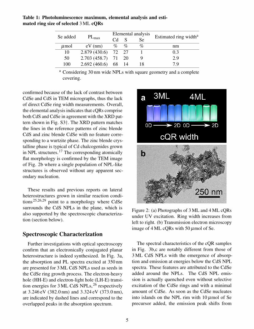
Table 1: Photoluminescence maximum, elemental analysis and esti-mated ring size of selected 3 ML cQRs
Se added PLmaxElemental analysis
Estimated ring widthaCd S Se
µmol eV (nm) % % % nm10 2.879 (430.6) 72 27 1 0.350 2.703 (458.7) 71 20 9 2.9
100 2.692 (460.6) 68 14 18 7.9a Considering 30 nm wide NPLs with square geometry and a complete
covering.
confirmed because of the lack of contrast betweenCdSe and CdS in TEM micrographs, thus the lackof direct CdSe ring width measurements. Overall,the elemental analysis indicates that cQRs compriseboth CdS and CdSe in agreement with the XRD pat-tern shown in Fig. S3†. The XRD pattern matchesthe lines in the reference patterns of zinc blendeCdS and zinc blende CdSe with no feature corre-sponding to a wurtzite phase. The zinc blende crys-talline phase is typical of Cd chalcogenides grownin NPL structures.17 The corresponding atomicallyflat morphology is confirmed by the TEM imageof Fig. 2b where a single population of NPL-likestructures is observed without any apparent sec-ondary nucleation.
These results and previous reports on lateralheterostructures grown in similar reaction condi-tions25,26,29 point to a morphology where CdSesurrounds the CdS NPLs in the plane, which isalso supported by the spectroscopic characteriza-tion (section below).
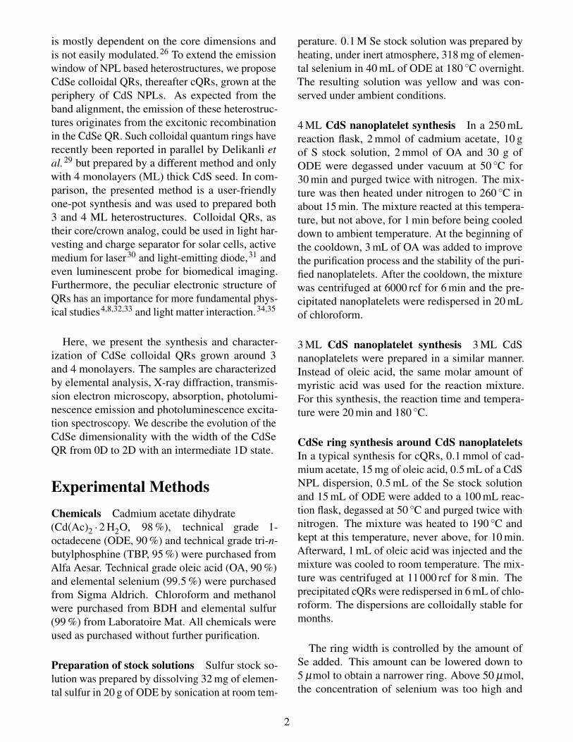
Spectroscopic CharacterizationFurther investigations with optical spectroscopy
confirm that an electronically conjugated planarheterostructure is indeed synthesized. In Fig. 3a,the absorption and PL spectra excited at 350 nmare presented for 3 ML CdS NPLs used as seeds inthe CdSe ring growth process. The electron-heavyhole (HH-E) and electron-light hole (LH-E) transi-tion energies for 3 ML CdS NPLs,26 respectivelyat 3.246 eV (382.0 nm) and 3.324 eV (373.0 nm),are indicated by dashed lines and correspond to theoverlapped peaks in the absorption spectrum.
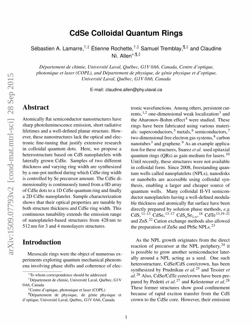
Figure 2: (a) Photographs of 3 ML and 4 ML cQRsunder UV excitation. Ring width increases fromleft to right. (b) Transmission electron microscopyimage of 4 ML cQRs with 50 µmol of Se.
The spectral characteristics of the cQR samplesin Fig. 3b,c are notably different from those of3 ML CdS NPLs with the emergence of absorp-tion and emission at energies below the CdS NPLspectra. These features are attributed to the CdSeadded around the NPLs. The CdS NPL emis-sion is actually quenched even without selectiveexcitation of the CdSe rings and with a minimalamount of CdSe. As soon as the CdSe nucleatesinto islands on the NPL rim with 10 µmol of Seprecursor added, the emission peak shifts from
5
350 400 450 500 550 600
Cd
S L
H−
E
Cd
S H
H−
E
Cd
Se
LH
−E
Cd
Se
HH
−E
a) CdS NPLs
Wavelength [nm]
b) CdS/CdSe cQRs 10 µmol of Se
Photo
lum
inescence [arb
. un.]
Extin
ctio
n [−
]
AbsPL
PLE
2.0 2.5 3.0 3.5 4.0
c) CdS/CdSe cQRs 200 µmol of Se
Energy [eV]
Figure 3: Absorption, photoluminescence and pho-toluminescence excitation spectra of (a) 3 ML CdSnanoplatelets, (b) 3 ML cQRs with 10 µmol of Seand (c) 3 ML cQRs with 200 µmol of Se. HH-E and LH-E transitions for 3 ML CdS and CdSeNPLs26 are identified with dotted lines.
3.220 eV (385.0 nm) to 2.861 eV (433.4 nm) witha final FWHM of 215 meV (32.6 nm) between Fig.3a and Fig. 3b. When the Se amount reaches200 µmol in Fig. 3c, the PL emission peak hasredshifted down to the energy of the HH-E tran-sition of CdSe NPLs at 2.67 eV (464 nm), with aFWHM of 57 meV (9.8 nm), also typical of atomi-cally flat 2D CdSe NPLs. The low energy emissiontail originating from trap states in islands with alarge surface-to-volume ratio has also disappeared.An extra peak is then observed at 2.43 eV (510 nm)and is attributed to thicker 4 ML CdSe 2D nanos-tructures either grown around thicker CdS sec-ondary nucleation or direct CdSe structure nucle-ation. For 200 µmol sample, the absorption spec-trum now features LH-E (2.863 eV, 433.1 nm) andHH-E (2.695 eV, 460.1 eV) transitions correspond-ing to isolated 3 ML CdSe NPLs and the combinedLH-E and HH-E transitions (3.29 eV, 377 nm) of3 ML CdS NPLs as labeled in Fig. 3.26 The photo-luminescence excitation spectrum with a detection
window centered on the PL maximum is also pro-vided in each panel to show its close match to theabsorption spectrum from the CdSe band edge upto 3.5 eV (350 nm).
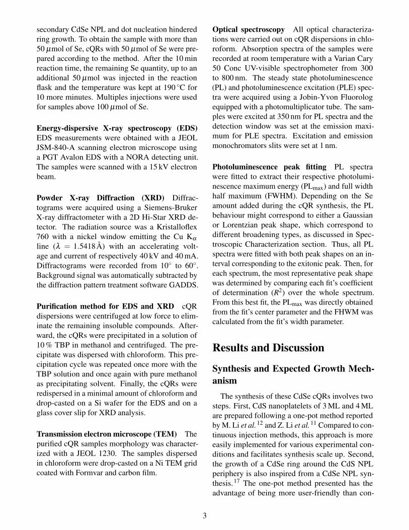
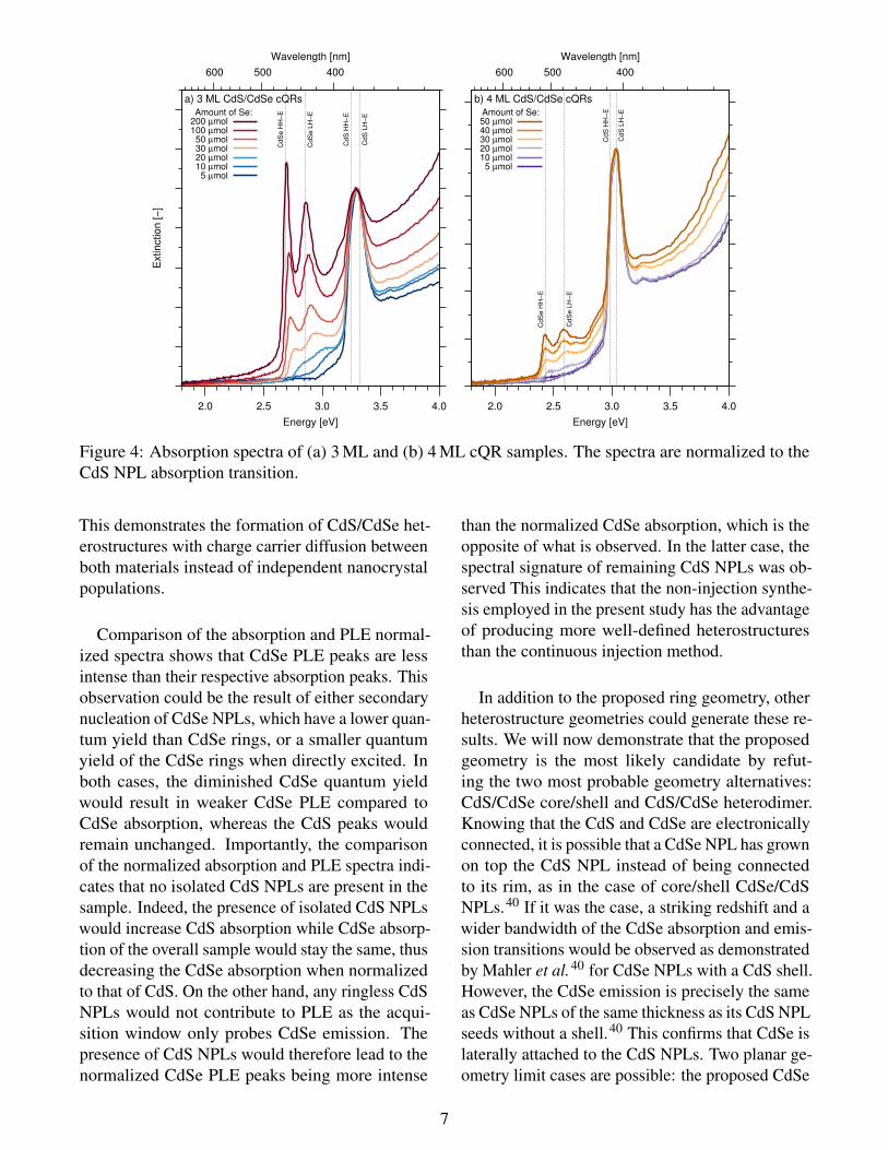
While Fig. 3b,c give an overview of the spectralcharacterizations done at both extreme Se amountsfor 3 ML CdS/CdSe heterostructures, the next Fig.4-6 show the detail of those measurements for allSe doses and heterostructure thicknesses. In Fig.4, the CdSe absorption features gradually appearas more CdSe is grown around the CdS NPLs forboth 3 ML and 4 ML CdS NPLs. The CdSe is moreapparent for 3 ML samples as the CdS NPL seedsused are smaller than the 4 ML ones. With smallSe amount, the CdSe absorption is very weak andonly one absorption peak can be seen. Starting at20 µmol, the HH-E and LH-E transitions are morevisible but they are much larger and blue-shiftedthan those expected for CdSe NPLs. At 200 µmol,the transitions have shifted back to the characteris-tic energies of CdSe NPL transitions. PLE spectrashowing equivalent behaviour are presented in Fig.S4†. PL spectra for all Se amounts and thicknessesare shown in Fig.5, in which both the PLmax andFWHM shifts are apparent. To extract quantitativeinformation about those shifts, the PL spectra werefitted as described in the Experimental Methodssection. The best fit PLmax and FWHM are shownin Fig. 6. These quantities are correlated, for boththicknesses: as the PLmax shifts to the lower en-ergy, so does the FWHM. The best fit for lower Seamount PL spectra was systematically the Gaussianpeak shape, while the Lorentzian peak shape wasmore suited to the higher Se dose PL spectra. Foreach thickness, the PLmax and FWHM shifts are re-duced after the change from Gaussian to Lorentzianpeak shape.
The equivalence between the absorption and PLEspectra is shown in Fig. 3 and can be inferredby comparing Fig. 4 and S2. This is attributedto ultrafast non-radiative relaxation bringing thephotogenerated charge carriers to the lowest ex-cited and emissive states in CdSe near the bandedge where the PLE signal is recorded,39 resultingin the CdS PL quenching. This is coherent withTessier et al.26 works with CdSe/CdS core/crown.
6
2.0 2.5 3.0 3.5 4.0
400 500 600
Cd
S L
H−
E
Cd
S H
H−
E
Cd
Se
LH
−E
Cd
Se
HH
−E
a) 3 ML CdS/CdSe cQRs
Extin
ctio
n [
−]
Energy [eV]
Wavelength [nm]
Amount of Se:
5 µmol10 µmol20 µmol30 µmol50 µmol
100 µmol200 µmol
2.0 2.5 3.0 3.5 4.0
400 500 600
b) 4 ML CdS/CdSe cQRs
Cd
S L
H−
E
Cd
S H
H−
E
Cd
Se
LH
−E
Cd
Se
HH
−E
Energy [eV]
Wavelength [nm]
Amount of Se:
5 µmol10 µmol20 µmol30 µmol40 µmol50 µmol
Figure 4: Absorption spectra of (a) 3 ML and (b) 4 ML cQR samples. The spectra are normalized to theCdS NPL absorption transition.
This demonstrates the formation of CdS/CdSe het-erostructures with charge carrier diffusion betweenboth materials instead of independent nanocrystalpopulations.
Comparison of the absorption and PLE normal-ized spectra shows that CdSe PLE peaks are lessintense than their respective absorption peaks. Thisobservation could be the result of either secondarynucleation of CdSe NPLs, which have a lower quan-tum yield than CdSe rings, or a smaller quantumyield of the CdSe rings when directly excited. Inboth cases, the diminished CdSe quantum yieldwould result in weaker CdSe PLE compared toCdSe absorption, whereas the CdS peaks wouldremain unchanged. Importantly, the comparisonof the normalized absorption and PLE spectra indi-cates that no isolated CdS NPLs are present in thesample. Indeed, the presence of isolated CdS NPLswould increase CdS absorption while CdSe absorp-tion of the overall sample would stay the same, thusdecreasing the CdSe absorption when normalizedto that of CdS. On the other hand, any ringless CdSNPLs would not contribute to PLE as the acqui-sition window only probes CdSe emission. Thepresence of CdS NPLs would therefore lead to thenormalized CdSe PLE peaks being more intense
than the normalized CdSe absorption, which is theopposite of what is observed. In the latter case, thespectral signature of remaining CdS NPLs was ob-served This indicates that the non-injection synthe-sis employed in the present study has the advantageof producing more well-defined heterostructuresthan the continuous injection method.
In addition to the proposed ring geometry, otherheterostructure geometries could generate these re-sults. We will now demonstrate that the proposedgeometry is the most likely candidate by refut-ing the two most probable geometry alternatives:CdS/CdSe core/shell and CdS/CdSe heterodimer.Knowing that the CdS and CdSe are electronicallyconnected, it is possible that a CdSe NPL has grownon top the CdS NPL instead of being connectedto its rim, as in the case of core/shell CdSe/CdSNPLs.40 If it was the case, a striking redshift and awider bandwidth of the CdSe absorption and emis-sion transitions would be observed as demonstratedby Mahler et al.40 for CdSe NPLs with a CdS shell.However, the CdSe emission is precisely the sameas CdSe NPLs of the same thickness as its CdS NPLseeds without a shell.40 This confirms that CdSe islaterally attached to the CdS NPLs. Two planar ge-ometry limit cases are possible: the proposed CdSe
7
400 450 500 550 600 650
a) 3 ML CdS/CdSe cQRsP
ho
tolu
min
esce
nce
[a
rb.
un
.]
Wavelength [nm]
Amount of Se:
5 µmol10 µmol20 µmol30 µmol40 µmol50 µmol
100 µmol
1.8 2.0 2.2 2.4 2.6 2.8 3.0 3.2 3.4
b) 4 ML CdS/CdSe cQRs
Energy [eV]
Amount of Se:
5 µmol10 µmol20 µmol30 µmol40 µmol50 µmol
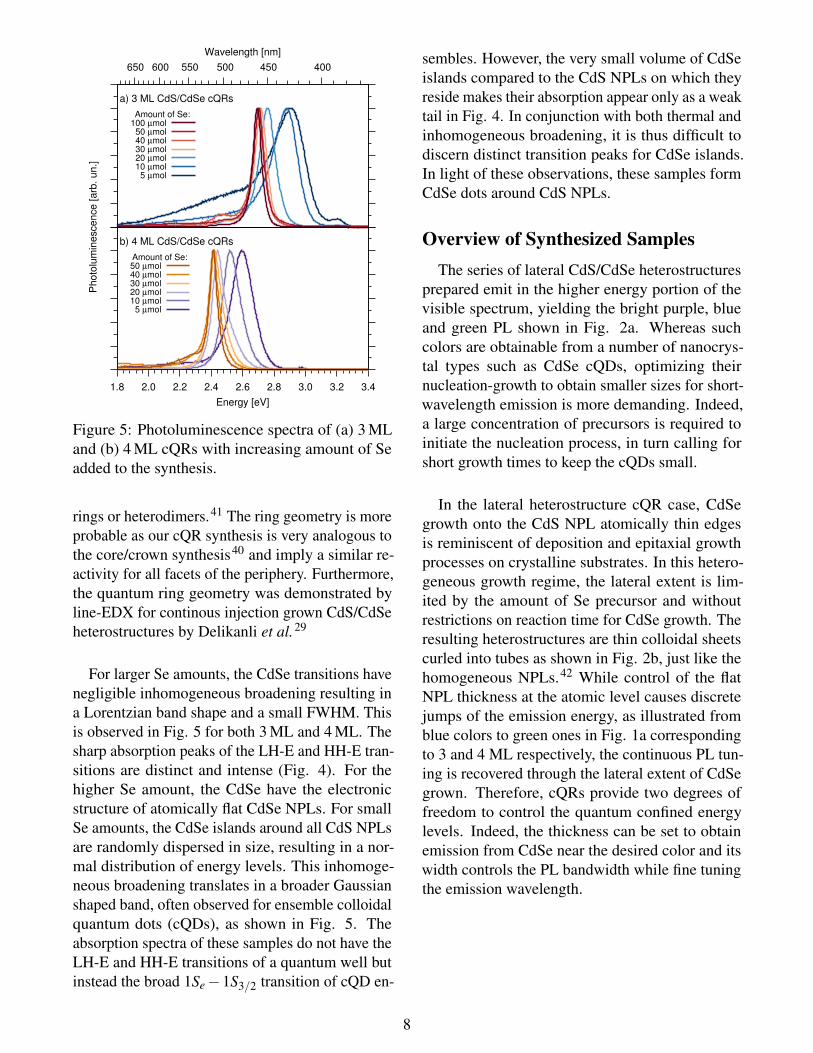
Figure 5: Photoluminescence spectra of (a) 3 MLand (b) 4 ML cQRs with increasing amount of Seadded to the synthesis.
rings or heterodimers.41 The ring geometry is moreprobable as our cQR synthesis is very analogous tothe core/crown synthesis40 and imply a similar re-activity for all facets of the periphery. Furthermore,the quantum ring geometry was demonstrated byline-EDX for continous injection grown CdS/CdSeheterostructures by Delikanli et al.29
For larger Se amounts, the CdSe transitions havenegligible inhomogeneous broadening resulting ina Lorentzian band shape and a small FWHM. Thisis observed in Fig. 5 for both 3 ML and 4 ML. Thesharp absorption peaks of the LH-E and HH-E tran-sitions are distinct and intense (Fig. 4). For thehigher Se amount, the CdSe have the electronicstructure of atomically flat CdSe NPLs. For smallSe amounts, the CdSe islands around all CdS NPLsare randomly dispersed in size, resulting in a nor-mal distribution of energy levels. This inhomoge-neous broadening translates in a broader Gaussianshaped band, often observed for ensemble colloidalquantum dots (cQDs), as shown in Fig. 5. Theabsorption spectra of these samples do not have theLH-E and HH-E transitions of a quantum well butinstead the broad 1Se−1S3/2 transition of cQD en-
sembles. However, the very small volume of CdSeislands compared to the CdS NPLs on which theyreside makes their absorption appear only as a weaktail in Fig. 4. In conjunction with both thermal andinhomogeneous broadening, it is thus difficult todiscern distinct transition peaks for CdSe islands.In light of these observations, these samples formCdSe dots around CdS NPLs.
Overview of Synthesized SamplesThe series of lateral CdS/CdSe heterostructures
prepared emit in the higher energy portion of thevisible spectrum, yielding the bright purple, blueand green PL shown in Fig. 2a. Whereas suchcolors are obtainable from a number of nanocrys-tal types such as CdSe cQDs, optimizing theirnucleation-growth to obtain smaller sizes for short-wavelength emission is more demanding. Indeed,a large concentration of precursors is required toinitiate the nucleation process, in turn calling forshort growth times to keep the cQDs small.
In the lateral heterostructure cQR case, CdSegrowth onto the CdS NPL atomically thin edgesis reminiscent of deposition and epitaxial growthprocesses on crystalline substrates. In this hetero-geneous growth regime, the lateral extent is lim-ited by the amount of Se precursor and withoutrestrictions on reaction time for CdSe growth. Theresulting heterostructures are thin colloidal sheetscurled into tubes as shown in Fig. 2b, just like thehomogeneous NPLs.42 While control of the flatNPL thickness at the atomic level causes discretejumps of the emission energy, as illustrated fromblue colors to green ones in Fig. 1a correspondingto 3 and 4 ML respectively, the continuous PL tun-ing is recovered through the lateral extent of CdSegrown. Therefore, cQRs provide two degrees offreedom to control the quantum confined energylevels. Indeed, the thickness can be set to obtainemission from CdSe near the desired color and itswidth controls the PL bandwidth while fine tuningthe emission wavelength.
8
Wavefunction Dimensionality Evolu-tion
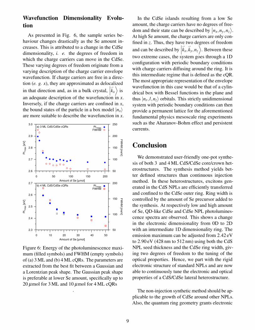
As presented in Fig. 6, the sample series be-haviour changes drastically as the Se amount in-creases. This is attributed to a change in the CdSedimensionality, i. e. the degrees of freedom inwhich the charge carriers can move in the CdSe.These varying degrees of freedom originate from avarying description of the charge carrier envelopewavefunction. If charge carriers are free in a direc-tion (e. g. x), they are approximated as delocalizedin that direction and, as in a bulk crystal,
∣∣∣⇀kx
⟩is
an adequate description of the wavefunction in x.Inversely, if the charge carriers are confined in x,the bound states of the particle in a box model |nx〉are more suitable to describe the wavefunction in x.
2.6
2.7
2.8
2.9
3.0
0 50 100 150 200
50
100
150
200
250a) 3 ML CdS/CdSe cQRs
PL
max [eV
]
FW
HM
[meV
]
Amount of Se [µmol]
PLmaxFWHM
2.3
2.4
2.5
2.6
2.7
0 10 20 30 40 50
50
100
150
200b) 4 ML CdS/CdSe cQRs
PL
max [eV
]
FW
HM
[meV
]
Amount of Se [µmol]
PLmaxFWHM
Figure 6: Energy of the photoluminescence maxi-mum (filled symbols) and FWHM (empty symbols)of (a) 3 ML and (b) 4 ML cQRs. The parameters areextracted from the best fit between a Gaussian anda Lorentzian peak shape. The Gaussian peak shapeis preferable at lower Se amount, specifically up to20 µmol for 3 ML and 10 µmol for 4 ML cQRs
.
In the CdSe islands resulting from a low Seamount, the charge carriers have no degrees of free-dom and their state can be described by
∣∣nx,ny,nz⟩.
At high Se amount, the charge carriers are only con-fined in z. Thus, they have two degrees of freedomand can be described by
∣∣∣⇀kx,⇀
ky,nz
⟩. Between these
two extreme cases, the system goes through a 1Dconfiguration with periodic boundary conditionswith charge carriers diffusing around the ring. It isthis intermediate regime that is defined as the cQR.The most appropriate representation of the envelopewavefunction in this case would be that of a cylin-drical box with Bessel functions in the plane andthus |nr, l,nz〉 orbitals. This strictly unidimensionalsystem with periodic boundary conditions can thenprovide a permanent lattice for the aforementionedfundamental physics mesoscale ring experimentssuch as the Aharanov-Bohm effect and persistentcurrents.
ConclusionWe demonstrated user-friendly one-pot synthe-
sis of both 3 and 4 ML CdS/CdSe core/crown het-erostructures. The synthesis method yields bet-ter defined structures than continuous injectionmethod. In these heterostructures, excitons gen-erated in the CdS NPLs are efficiently transferredand confined to the CdSe outer ring. Ring width iscontrolled by the amount of Se precursor added tothe synthesis. At respectively low and high amountof Se, QD-like CdSe and CdSe NPL photolumines-cence spectra are observed. This shows a changein the electronic dimensionality from 0D to 2Dwith an intermediate 1D dimensionality ring. Theemission maximum can be adjusted from 2.42 eVto 2.90 eV (428 nm to 512 nm) using both the CdSNPL seed thickness and the CdSe ring width, giv-ing two degrees of freedom to the tuning of theoptical properties. Hence, we part with the rigidelectronic structure of standard NPLs and are nowable to continuously tune the electronic and opticalproperties of a CdS/CdSe lateral heterostructure.
The non-injection synthetic method should be ap-plicable to the growth of CdSe around other NPLs.Also, the quantum ring geometry grants electronic
9
structure fine-tuning to NPLs that, despite their ad-vantages over cQDs, could only be discretely tuned.As such, this geometry could advantageously beapplied to other II-VI semiconductors than CdSe.Furthermore, quantum rings could be synthesizedwith semiconductor alloys, which would lead toan even greater control over their band alignment.While this article identified the 0D and 2D geome-tries in photoluminescence and absorption spectra,the 1D quantum ring state was only interpolated.An extensive study of these spectra with fine varia-tion of Se amount around the observed shift from0D to 2D behavior is needed to systematically syn-thesize true 1D heterostructure.
Acknowledgement The research was supportedby National Science and Engineering ResearchCouncil(NSERC). The authors thank PatrickLarochelle for technical support, Denis Boudreaufor sharing experimental equipment, and DominicLarivière as well as Anna Ritcey for their inputs onthe manuscript and interesting discussions.
Supplementary materials: Five figures: TEMmicrographs for 3 ML sample, EDS analysis ex-ample, X-ray diffractogram, PLE spectra for eachsample, and relation between PLmax and FWHM.
References(1) Gunther, L.; Imry, Y. Flux quantization with-
out off-diagonal long range order in a thinhollow cylinder. Solid State Communications1969, 7, 1391–1394.
(2) Büttiker, M.; Imry, Y.; Landauer, R.Josephson behavior in small normal one-dimensional rings. Physics Letters A 1983,96, 365–367.
(3) Shea, H.; Martel, R.; Avouris, P. Electricaltransport in rings of single-wall nanotubes:one-dimensional localization. Physical reviewletters 2000, 84, 4441.
(4) Keyser, U.; Borck, S.; Haug, R.; Bichler, M.;Abstreiter, G.; Wegscheider, W. Aharonov–Bohm oscillations of a tuneable quantum ring.Semiconductor Science and Technology 2002,17, L22.
(5) Doll, R.; Nabauer, M. Experimental proof ofmagnetic flux quantization in a superconduct-ing ring. Phys. Rev. Letters 1961, 7.
(6) Washburn, S.; Webb, R. A. Aharonov-Bohmeffect in normal metal quantum coherenceand transport. Advances in Physics 1986, 35,375–422.
(7) Granados, D.; Garcìa, J. M. In (Ga) As self-assembled quantum ring formation by molec-ular beam epitaxy. Applied physics letters2003, 82, 2401–2403.
(8) Fuhrer, A.; Lüscher, S.; Ihn, T.; Heinzel, T.;Ensslin, K.; Wegscheider, W.; Bichler, M. En-ergy spectra of quantum rings. Nature 2001,413, 822–825.
(9) Potasz, P.; Güçlü, A.; Voznyy, O.; Folk, J.;Hawrylak, P. Electronic and magnetic prop-erties of triangular graphene quantum rings.Physical Review B 2011, 83, 174441.
(10) Suárez, F.; Granados, D.; Dotor, M. L.; Gar-cia, J. M. Laser devices with stacked layers ofInGaAs/GaAs quantum rings. Nanotechnol-ogy 2004, 15, S126.
(11) Li, Z.; Qin, H.; Guzun, D.; Benamara, M.;Salamo, G.; Peng, X. Uniform thicknessand colloidal-stable CdS quantum disks withtunable thickness: Synthesis and properties.Nano Research 2012, 5, 337–351.
(12) Li, M.; Ouyang, J.; Ratcliffe, C. I.; Pietri, L.;Wu, X.; Leek, D. M.; Moudrakovski, I.;Lin, Q.; Yang, B.; Yu, K. CdS magic-sizednanocrystals exhibiting bright band gap pho-toemission via thermodynamically driven for-mation. ACS nano 2009, 3, 3832–3838.
(13) Ithurria, S.; Tessier, M.; Mahler, B.;Lobo, R.; Dubertret, B.; Efros, A. L. Col-loidal nanoplatelets with two-dimensionalelectronic structure. Nature materials 2011,10, 936–941.
(14) Ithurria, S.; Dubertret, B. Quasi 2D colloidalCdSe platelets with thicknesses controlled atthe atomic level. Journal of the AmericanChemical Society 2008, 130, 16504–16505.
10
(15) Yu, K.; Ouyang, J.; Zaman, M. B.; John-ston, D.; Yan, F. J.; Li, G.; Ratcliffe, C. I.;Leek, D. M.; Wu, X.; Stupak, J. et al. Single-sized CdSe nanocrystals with bandgap photoe-mission via a noninjection one-pot approach.The Journal of Physical Chemistry C 2009,113, 3390–3401.
(16) Ouyang, J.; Zaman, M. B.; Yan, F. J.; John-ston, D.; Li, G.; Wu, X.; Leek, D.; Rat-cliffe, C. I.; Ripmeester, J. A.; Yu, K. Multi-ple families of magic-sized CdSe nanocrystalswith strong bandgap photoluminescence vianoninjection one-pot syntheses. The Journalof Physical Chemistry C 2008, 112, 13805–13811.
(17) Li, Z.; Peng, X. Size/shape-controlled synthe-sis of colloidal CdSe quantum disks: Ligandand temperature effects. Journal of the Ameri-can Chemical Society 2011, 133, 6578–6586.
(18) Fan, F.; Kanjanaboos, P.; Saravanapavanan-tham, M.; Beauregard, E.; Ingram, G.; Yas-sitepe, E.; Adachi, M. M.; Voznyy, O.; John-ston, A. K.; Walters, G. W. et al. ColloidalCdSe1-xSx Nanoplatelets with Narrow andContinuously-Tunable Electroluminescence.Nano Letters 2015,
(19) Wang, J.; Zhai, J.; Han, S. Non-injection one-pot preparation strategy for multiple fami-lies of magic-sized CdTe quantum dots withbright bandgap photoemission. Chemical En-gineering Journal 2013, 215, 23–28.
(20) Wang, R.; Ouyang, J.; Nikolaus, S.;Brestaz, L.; Zaman, M. B.; Wu, X.; Leek, D.;Ratcliffe, C. I.; Yu, K. Single-sized colloidalCdTe nanocrystals with strong bandgap pho-toluminescence. Chemical Communications2009, 962–964.
(21) Pedetti, S.; Nadal, B.; Lhuillier, E.;Mahler, B.; Bouet, C.; Abécassis, B.; Xu, X.;Dubertret, B. Optimized Synthesis of CdTeNanoplatelets and Photoresponse of CdTeNanoplatelets Films. Chemistry of Materials2013, 25, 2455–2462.
(22) Buffard, A.; Nadal, B.; Heuclin, H.; Pa-triarche, G.; Dubertret, B. ZnS anisotropic
nanocrystals using a one-pot low temperaturesynthesis. New Journal of Chemistry 2015,39, 90–93.
(23) Bouet, C.; Laufer, D.; Mahler, B.; Nadal, B.;Heuclin, H.; Pedetti, S.; Patriarche, G.; Du-bertret, B. Synthesis of Zinc and Lead Chalco-genide Core and Core/Shell Nanoplatelets Us-ing Sequential Cation Exchange Reactions.Chemistry of Materials 2014, 26, 3002–3008.
(24) Ithurria, S.; Bousquet, G.; Dubertret, B. Con-tinuous transition from 3D to 1D confine-ment observed during the formation of CdSenanoplatelets. Journal of the American Chem-ical Society 2011, 133, 3070–3077.
(25) Prudnikau, A.; Chuvilin, A.; Artemyev, M.CdSe–CdS Nanoheteroplatelets with Effi-cient Photoexcitation of Central CdSe Regionthrough Epitaxially Grown CdS Wings. Jour-nal of the American Chemical Society 2013,135, 14476–14479.
(26) Tessier, M. D.; Spinicelli, P.; Dupont, D.; Pa-triarche, G.; Ithurria, S.; Dubertret, B. Effi-cient Exciton Concentrators Built from Col-loidal Core/Crown CdSe/CdS SemiconductorNanoplatelets. Nano letters 2013, 14, 207–213.
(27) Pedetti, S.; Ithurria, S.; Heuclin, H.; Patri-arche, G.; Dubertret, B. Type-II CdSe/CdTeCore/Crown Semiconductor Nanoplatelets.Journal of the American Chemical Society2014, 136, 16430–16438.
(28) Kelestemur, Y.; Olutas, M.; Delikanli, S.;Guzelturk, B.; Akgul, M. Z.; Demir, H. V.Type-II Colloidal Quantum Wells:CdSe/CdTe Core/Crown Heteronanoplatelets.The Journal of Physical Chemistry C 2015,119, 2177–2185.
(29) Delikanli, S.; Guzelturk, B.; Hernández-Martínez, P. L.; Erdem, T.; Kelestemur, Y.;Olutas, M.; Akgul, M. Z.; Demir, H. V.Continuously Tunable Emission in InvertedType-I CdS/CdSe Core/Crown Semiconduc-tor Nanoplatelets. Advanced Functional Ma-terials 2015,
11
(30) Guzelturk, B.; Kelestemur, Y.; Olutas, M.;Delikanli, S.; Demir, H. V. Amplified spon-taneous emission and lasing in colloidalnanoplatelets. ACS nano 2014, 8, 6599–6605.
(31) Vashchenko, A.; Vitukhnovskii, A.; Lebe-dev, V. S.; Selyukov, A.; Vasiliev, R. B.; Soko-likova, M. Organic light-emitting diode withan emitter based on a planar layer of CdSesemiconductor nanoplatelets. JETP Letters2014, 100, 86–90.
(32) Orellana, P.; De Guevara, M. L.; Pacheco, M.;Latge, A. Conductance and persistent currentof a quantum ring coupled to a quantum wireunder external fields. Physical Review B 2003,68, 195321.
(33) Bayer, M.; Korkusinski, M.; Hawrylak, P.;Gutbrod, T.; Michel, M.; Forchel, A. Opticaldetection of the Aharonov-Bohm effect on acharged particle in a nanoscale quantum ring.Physical review letters 2003, 90, 186801.
(34) Sen, S.; Das, N.; Chakravarti, A. Electronemission from a semiconductor quantum ringunder normally incident radiation. Journalof Physics: Condensed Matter 2007, 19,186205.
(35) Warburton, R. J.; Schulhauser, C.; Haft, D.;Schäflein, C.; Karrai, K.; Garcia, J. M.;Schoenfeld, W.; Petroff, P. M. Giant perma-nent dipole moments of excitons in semi-conductor nanostructures. Physical Review B2002, 65, 113303.
(36) Srivastava, B. B.; Jana, S.; Sarma, D.; Prad-han, N. Surface ligand population controlledoriented attachment: a case of CdS nanowires.The Journal of Physical Chemistry Letters2010, 1, 1932–1935.
(37) Yu, K.; Hu, M. Z.; Wang, R.; Pio-let, M. L.; Frotey, M.; Zaman, M. B.; Wu, X.;Leek, D. M.; Tao, Y.; Wilkinson, D. et al.Thermodynamic equilibrium-driven forma-tion of single-sized nanocrystals: reaction me-dia tuning CdSe magic-sized versus regularquantum dots. The Journal of Physical Chem-istry C 2010, 114, 3329–3339.
(38) Yu, K. CdSe Magic-Sized Nuclei, Magic-Sized Nanoclusters and Regular Nanocrystals:Monomer Effects on Nucleation and Growth.Advanced Materials 2012, 24, 1123–1132.
(39) Tonti, D.; Van Mourik, F.; Chergui, M. On theexcitation wavelength dependence of the lu-minescence yield of colloidal CdSe quantumdots. Nano Letters 2004, 4, 2483–2487.
(40) Mahler, B.; Nadal, B.; Bouet, C.; Patri-arche, G.; Dubertret, B. Core/Shell col-loidal semiconductor nanoplatelets. Journalof the American Chemical Society 2012, 134,18591–18598.
(41) De Trizio, L.; Figuerola, A.; Manna, L.; Gen-ovese, A.; George, C.; Brescia, R.; Saghi, Z.;Simonutti, R.; Van Huis, M.; Falqui, A.Size-Tunable, Hexagonal Plate-like Cu3P andJanus-like Cu–Cu3P Nanocrystals. ACS nano2011, 6, 32–41.
(42) Bouet, C.; Mahler, B.; Nadal, B.; Abecas-sis, B.; Tessier, M. D.; Ithurria, S.; Xu, X.;Dubertret, B. Two-dimensional growth ofCdSe nanocrystals, from nanoplatelets tonanosheets. Chemistry of Materials 2013, 25,639–645.
12