Embed Size (px)
Citation preview
Central Processing Unit General Register Organization Stack Organization Instruction Formats Addressing Modes Data Transfer and Manipulation Micro Programmed Control Reduced Instruction Set Computer Parallel Processing Pipelining Arithmetic Pipeline Instruction Pipeline RISC Pipeline Vector Processing Array Processes
�������
Central Processing Unit
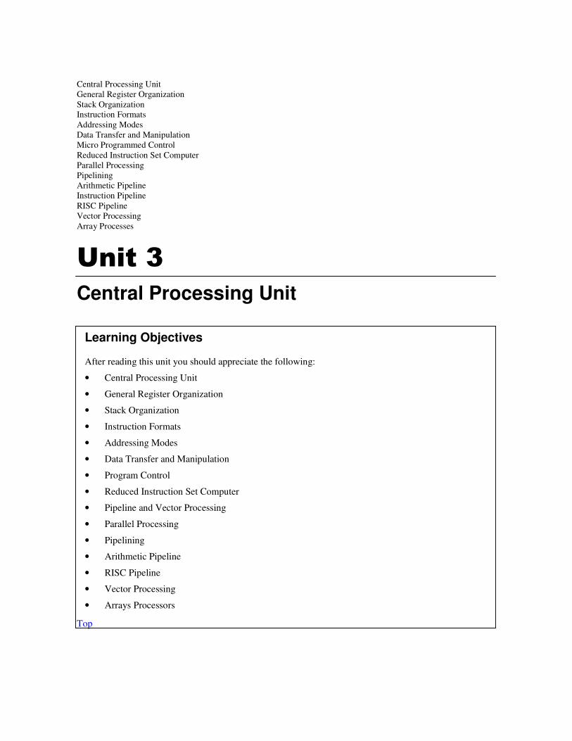
Learning Objectives
After reading this unit you should appreciate the following:
• Central Processing Unit
• General Register Organization
• Stack Organization
• Instruction Formats
• Addressing Modes
• Data Transfer and Manipulation
• Program Control
• Reduced Instruction Set Computer
• Pipeline and Vector Processing
• Parallel Processing
• Pipelining
• Arithmetic Pipeline
• RISC Pipeline
• Vector Processing
• Arrays Processors
Top
COMPUTER SYSTEM ARCHITECTURE 66
������� ��������������
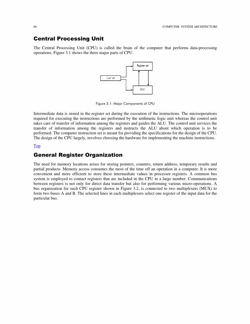
The Central Processing Unit (CPU) is called the brain of the computer that performs data-processing operations. Figure 3.1 shows the three major parts of CPU.
�
����������� ������� ���������������
Intermediate data is stored in the register set during the execution of the instructions. The microoperations required for executing the instructions are performed by the arithmetic logic unit whereas the control unit takes care of transfer of information among the registers and guides the ALU. The control unit services the transfer of information among the registers and instructs the ALU about which operation is to be performed. The computer instruction set is meant for providing the specifications for the design of the CPU. The design of the CPU largely, involves choosing the hardware for implementing the machine instructions.
Top
��������������������� ��
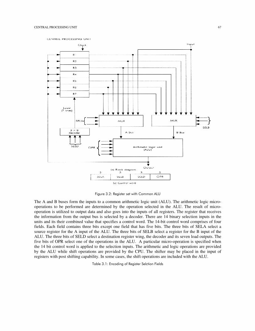
The need for memory locations arises for storing pointers, counters, return address, temporary results and partial products. Memory access consumes the most of the time off an operation in a computer. It is more convenient and more efficient to store these intermediate values in processor registers. A common bus system is employed to contact registers that are included in the CPU in a large number. Communications between registers is not only for direct data transfer but also for performing various micro-operations. A bus organization for such CPU register shown in Figure 3.2, is connected to two multiplexers (MUX) to form two buses A and B. The selected lines in each multiplexers select one register of the input data for the particular bus.
CENTRAL PROCESSING UNIT 67
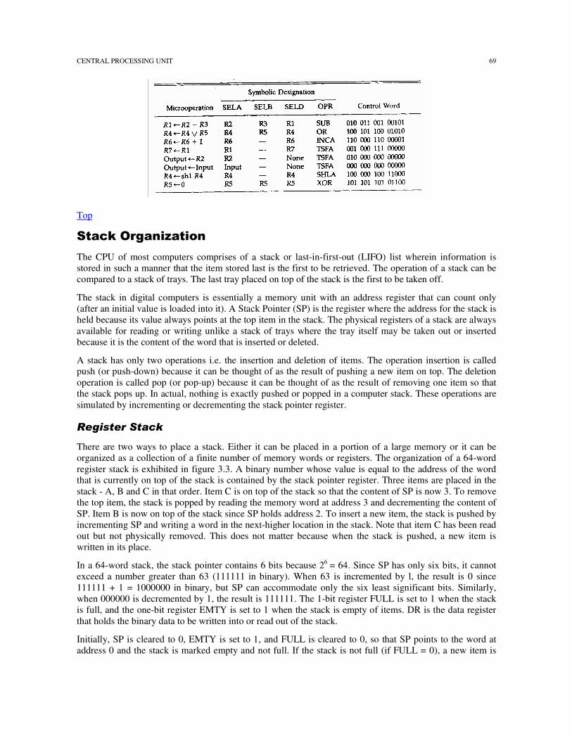
�������������������������������� � �������
The A and B buses form the inputs to a common arithmetic logic unit (ALU). The arithmetic logic micro-operations to be performed are determined by the operation selected in the ALU. The result of micro-operation is utilized to output data and also goes into the inputs of all registers. The register that receives the information from the output bus is selected by a decoder. There are 14 binary selection inputs in the units and its their combined value that specifies a control word. The 14-bit control word comprises of four fields. Each field contains three bits except one field that has five bits. The three bits of SELA select a source register for the A input of the ALU. The three bits of SELB select a register for the B input of the ALU. The three bits of SELD select a destination register wing, the decoder and its seven load outputs. The five bits of OPR select one of the operations in the ALU. A particular micro-operation is specified when the 14 bit control word is applied to the selection inputs. The arithmetic and logic operations are provided by the ALU while shift operations are provided by the CPU. The shifter may be placed in the input of registers with post shifting capability. In some cases, the shift operations are included with the ALU.
� !�����"�#�$����������������%�!#��������!$��
COMPUTER SYSTEM ARCHITECTURE 68
� !������"�#�$�����������& ��� ������
�
���������� ������� ��
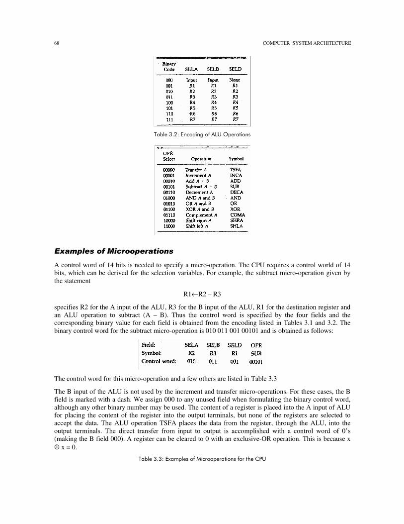
A control word of 14 bits is needed to specify a micro-operation. The CPU requires a control world of 14 bits, which can be derived for the selection variables. For example, the subtract micro-operation given by the statement
R1←R2 – R3
specifies R2 for the A input of the ALU, R3 for the B input of the ALU, R1 for the destination register and an ALU operation to subtract (A – B). Thus the control word is specified by the four fields and the corresponding binary value for each field is obtained from the encoding listed in Tables 3.1 and 3.2. The binary control word for the subtract micro-operation is 010 011 001 00101 and is obtained as follows:
The control word for this micro-operation and a few others are listed in Table 3.3
The B input of the ALU is not used by the increment and transfer micro-operations. For these cases, the B field is marked with a dash. We assign 000 to any unused field when formulating the binary control word, although any other binary number may be used. The content of a register is placed into the A input of ALU for placing the content of the register into the output terminals, but none of the registers are selected to accept the data. The ALU operation TSFA places the data from the register, through the ALU, into the output terminals. The direct transfer from input to output is accomplished with a control word of 0’s (making the B field 000). A register can be cleared to 0 with an exclusive-OR operation. This is because x ⊕ x = 0.
� !������"' � �!������� �#������ ������������������
CENTRAL PROCESSING UNIT 69
�
Top
������������ ��
The CPU of most computers comprises of a stack or last-in-first-out (LIFO) list wherein information is stored in such a manner that the item stored last is the first to be retrieved. The operation of a stack can be compared to a stack of trays. The last tray placed on top of the stack is the first to be taken off.
The stack in digital computers is essentially a memory unit with an address register that can count only (after an initial value is loaded into it). A Stack Pointer (SP) is the register where the address for the stack is held because its value always points at the top item in the stack. The physical registers of a stack are always available for reading or writing unlike a stack of trays where the tray itself may be taken out or inserted because it is the content of the word that is inserted or deleted.
A stack has only two operations i.e. the insertion and deletion of items. The operation insertion is called push (or push-down) because it can be thought of as the result of pushing a new item on top. The deletion operation is called pop (or pop-up) because it can be thought of as the result of removing one item so that the stack pops up. In actual, nothing is exactly pushed or popped in a computer stack. These operations are simulated by incrementing or decrementing the stack pointer register.
��� ���������
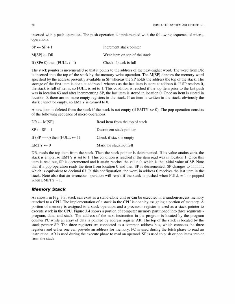
There are two ways to place a stack. Either it can be placed in a portion of a large memory or it can be organized as a collection of a finite number of memory words or registers. The organization of a 64-word register stack is exhibited in figure 3.3. A binary number whose value is equal to the address of the word that is currently on top of the stack is contained by the stack pointer register. Three items are placed in the stack - A, B and C in that order. Item C is on top of the stack so that the content of SP is now 3. To remove the top item, the stack is popped by reading the memory word at address 3 and decrementing the content of SP. Item B is now on top of the stack since SP holds address 2. To insert a new item, the stack is pushed by incrementing SP and writing a word in the next-higher location in the stack. Note that item C has been read out but not physically removed. This does not matter because when the stack is pushed, a new item is written in its place.
In a 64-word stack, the stack pointer contains 6 bits because 26 = 64. Since SP has only six bits, it cannot exceed a number greater than 63 (111111 in binary). When 63 is incremented by l, the result is 0 since 111111 + 1 = 1000000 in binary, but SP can accommodate only the six least significant bits. Similarly, when 000000 is decremented by 1, the result is 111111. The 1-bit register FULL is set to 1 when the stack is full, and the one-bit register EMTY is set to 1 when the stack is empty of items. DR is the data register that holds the binary data to be written into or read out of the stack.
Initially, SP is cleared to 0, EMTY is set to 1, and FULL is cleared to 0, so that SP points to the word at address 0 and the stack is marked empty and not full. If the stack is not full (if FULL = 0), a new item is
COMPUTER SYSTEM ARCHITECTURE 70
inserted with a push operation. The push operation is implemented with the following sequence of micro-operations:
SP ← SP + 1 Increment stack pointer
M[SP] ← DR Write item on top of the stack
If (SP= 0) then (FULL ← l) Check if stack is full
The stack pointer is incremented so that it points to the address of the next-higher word. The word from DR is inserted into the top of the stack by the memory write operation. The M[SP] denotes the memory word specified by the address presently available in SP whereas the SP holds the address the top of the stack. The storage of the first item is done at address 1 whereas as the last item is store at address 0. If SP reaches 0, the stack is full of items, so FULL is set to 1. This condition is reached if the top item prior to the last push was in location 63 and after incrementing SP, the last item is stored in location 0. Once an item is stored in location 0, there are no more empty registers in the stack. If an item is written in the stack, obviously the stack cannot be empty, so EMTY is cleared to 0.
A new item is deleted from the stack if the stack is not empty (if EMTY <> 0). The pop operation consists of the following sequence of micro-operations:
DR ← M[SP] Read item from the top of stack
SP ← SP – 1 Decrement stack pointer
If (SP == 0) then (FULL ← 1) Check if stack is empty
EMTY ← 0 Mark the stack not full
DR. reads the top item from the stack. Then the stack pointer is decremented. If its value attains zero, the stack is empty, so EMTY is set to 1. This condition is reached if the item read was in location 1. Once this item is read out, SP is decremented and it attain reaches the value 0, which is the initial value of SP. Note that if a pop operation reads the item from location 0 and then SP is decremented, SP changes to 111111, which is equivalent to decimal 63. In this configuration, the word in address 0 receives the last item in the stack. Note also that an erroneous operation will result if the stack is pushed when FULL = 1 or popped when EMPTY = 1.
����������
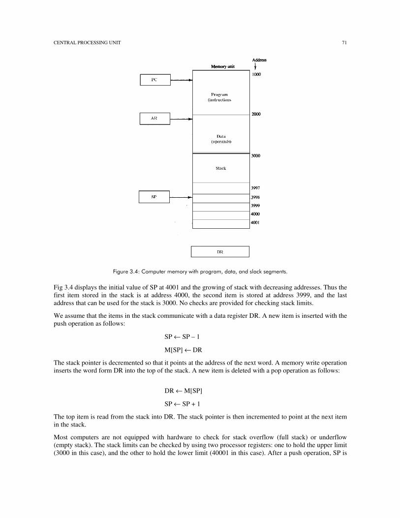
As shown in Fig. 3.3, stack can exist as a stand-alone unit or can be executed in a random-access memory attached to a CPU. The implementation of a stack in the CPU is done by assigning a portion of memory. A portion of memory is assigned to a stack operation and a processor register is used as a stack pointer to execute stack in the CPU. Figure 3.4 shows a portion of computer memory partitioned into three segments - program, data, and stack. The address of the next instruction in the program is located by the program counter PC while an array of data is pointed by address register AR. The top of the stack is located by the stack pointer SP. The three registers are connected to a common address bus, which connects the three registers and either one can provide an address for memory. PC is used during the fetch phase to read an instruction. AR is used during the execute phase to read an operand. SP is used to push or pop items into or from the stack.
CENTRAL PROCESSING UNIT 71
�
��������(����� ������� �� ��)����������� � *�$ � *� �$��! #+����� �����
Fig 3.4 displays the initial value of SP at 4001 and the growing of stack with decreasing addresses. Thus the first item stored in the stack is at address 4000, the second item is stored at address 3999, and the last address that can be used for the stack is 3000. No checks are provided for checking stack limits.
We assume that the items in the stack communicate with a data register DR. A new item is inserted with the push operation as follows:
SP ← SP – 1
M[SP] ← DR
The stack pointer is decremented so that it points at the address of the next word. A memory write operation inserts the word form DR into the top of the stack. A new item is deleted with a pop operation as follows:
DR ← M[SP]
SP ← SP + 1
The top item is read from the stack into DR. The stack pointer is then incremented to point at the next item in the stack.
Most computers are not equipped with hardware to check for stack overflow (full stack) or underflow (empty stack). The stack limits can be checked by using two processor registers: one to hold the upper limit (3000 in this case), and the other to hold the lower limit (40001 in this case). After a push operation, SP is
COMPUTER SYSTEM ARCHITECTURE 72
compared with the upper-limit register and after a pop operation, SP is compared with the lower-limit register.
Student Activity 3.1
Before you proceed with the next section, answer the following questions.
1. What are the major components of a control processing unit?
2. What do you mean by a control word? Describe the meaning of each field in a control word.
3. Describe the push and pop examples of a stack with suitable examples.
If your answers are correct, then proceed with the next section.
Top
�������� ��� � ���
The reference manuals provided with a computer system contain a description of its physical and logical structure. These manuals explain the internal construction of the CPU, including the processor registers available and their logical capabilities. All hardware-implemented instructions, their binary code format, and a precise definition of each instruction is very well described by these manuals. Given the fact that a computer has a variety of instruction code formats, it is the control unit within the CPU that interprets each instruction code and provides the necessary control functions needed to process the instruction.
The format of an instruction is usually depicted in a rectangular box symbolizing the bits of the instruction as they appear in memory words or in a control register. The bits of the instruction are divided into groups called fields. The most common fields found in instruction formats are:
1. An operation code field that specifies the operation to be performed.
2. An address field that designates a memory address or a processor register.
3. A mode field that specifies the way the operand or the effective address is determined.
At times other special fields are also employed sometimes employed as for example a field that gives the number of shifts in a shift-type instruction.
The operation code field of an instruction is referred to a group of bits that define various processor operations, such as add, subtract, complement, and shift. A variety of alternatives for choosing the operands from the given address is specified by the bits that define the mode field of the instruction code. Further ahead is the description about the address field on the instruction format and affect at including of multiple address field in instruction in the digital circuits In this section we are concerned with the address field of an instruction format and consider the effect of including multiple address fields in an instruction.
Execution of operations done by some data stored in memory or processor registers through specification received by computer instructions. A memory address specifies operands residing in memory whereas those residing in processor registers are specified by a register address. A register address is a binary number of k bits that defines one of 2k registers in the CPU. Thus a CPU with 16 processor registers R0 through R15 will have a register address field of four bits. The binary number 0101, for example, will designate register R5.
Instructions in computers can be of different lengths containing varying number of addresses. The internal organization of the registers of a computer determines the number of address fields in the instruction formats.. Most computers fall into one of three types of CPU organizations:
CENTRAL PROCESSING UNIT 73
1. Single accumulator organization.
2. General register organization.
3. Stack organization.
An example of an accumulator-type organization is the basic computer. All operations are performed with an implied accumulator register. The instruction format in this type of computer uses one address field. For example, the instruction that specifies an arithmetic addition is defined by an assembly language instruction as:
ADD X
where X is the address of the operand. The ADD instruction in this case results in the operation AC ←AC + M[X]. AC is the accumulator register and M[X] symbolizes the memory word located at address X.
An example of a general register type of organization was presented in Figure 3.2. The instruction format in this type of computer needs three register address fields. Thus, the instruction for an arithmetic addition may be written in an assembly language as:
ADD Rl, R2, R3
to denote the operation Rl ←R2 + R3. The number of address fields in the instruction can be reduced from three to two if the destination register is the same and one of the source registers. Thus, the instruction:
ADD Rl, R2
would denote the operational R1 ← R1 + R2. Only register addresses for R1 and R2 need to be specified in this instruction.
Computers with multiple processor registers use the move instruction with a mnemonic MOV to symbolize a transfer instruction. Thus the instruction:
MOV R1, R2
denotes the transfer R1 ←R2 (or R2←R1, depending on the particular computer). Thus, transfer-type instructions need two address fields to specify the source and the destination.
Usually only two or three address fields are employed general register-type computers in their instruction format. Each address field may specify a processor register or a memory word. An instruction symbolized by:
ADD R1, X
would specify the operation R1 ←R1+M[X]. It has two address fields, one for register R1 and the other for the memory address X.
Computers with stack organization would have PUSH and POP instructions which require an address field. Thus the instruction:
PUSH X
will push the word at address X to the top of the stack. The stack pointer is updated automatically. Operation-type instructions do not need an address field in stack-organized computers. This is because the operation is performed on the two items that are on top of the stack. The instruction:
ADD
COMPUTER SYSTEM ARCHITECTURE 74
in a stack computer consists of an operation code only with no address field. This operation has the effect of popping the two top numbers from the stack, adding the numbers, and pushing the sum into the stack. Since all operands are implied to be in the stack , the need for specifying operands with the address field does not arise .
Most of the computers comprise one of the three types of organizations that have just been described. Some computers combine features from more than one organizational structure. For instance, the Intel 8080 microprocessor has seven CPU registers, one of which is an accumulator register. Consequently, the processor exhibits some of the characteristics of a general register type and some of the characteristics of an accumulator type. All arithmetic and logic instructions, as well as the load and store instructions, use the accumulator register, so these instructions have only one address field. On the other hand, instructions that transfer data among the seven processor registers have a format that contains two register address fields. Moreover, the Intel 8080 processor has a stack pointer and instructions to push and pop from a memory stack. The processor, however, does not have the zero-address-type instructions which are characteristic of a stack-organized CPU.
To illustrate the influence of the number of addresses on computer programs, we will evaluate the arithmetic statement
X = (A + B)*(C + D)
using zero, one, two, or three address instructions. We will use the symbols ADD, SUB, MUL and DIV for the four arithmetic operations; MOV for the transfer-type operation; and LOAD and STORE for transfers to and from memory and AC register. We will assume that the operands are in memory addresses A, B, C, and D, and the result must be stored in memory at address X.
�������������������� ���
Computers with three-address instruction formats can use each address field to specify either a processor register or a memory operand. The program in assembly language that evaluates X = (A + B) * (C + D) is shown below, together with comments that explain the register transfer operation of each instruction.
ADD R1,A,B R1←M[A]+M[B]
ADD R2,C,D R2←M[C]+M[D]
MUL X,R1,R2 M[X] ←R1*R2
It is assumed that the computer has two processor registers, Rl and R2. The symbol M[A] denotes the operand at memory address symbolized by A.
The advantage of the three-address format is that it results in short programs when evaluating arithmetic expressions. The disadvantage is that the binary-coded instructions require too many bits to specify three addresses. An example of a commercial computer that uses three-address instructions is the Cyber 170. The instruction formats in the Cyber computer are restricted to either three register address fields or two register address fields and one memory address field.
� ���������������� ���
Two-address instructions are the most common in commercial computers. Here again each address field can specify either a processor register or memory word. The program to evaluate X = (A + B)* (C + D) is as follows:
MOV R1, A R1←M[A]
ADD R1, B R1←RI+M[B]
CENTRAL PROCESSING UNIT 75
MOV R2, C R2←M[C]
ADD R2,D R2←R2+M[D]
MUL R1,R2 R1←R1*RP
MOV X, R1 M[X] ← R1
The MOV instruction moves or transfers the operands to and from memory and processor registers. The first symbol listed in an instruction is assumed to be both a source and the destination where the result of the operation transferred.
������������������� ��
One-address instructions use an implied accumulator (AC) register for all data manipulation. For multiplication and division there is a need for a second register. However, here we will neglect the second register and assume that the AC contains the result of all operations. The program to evaluate X=(A+B)*(C+D)is:
LOAD A AC←M[A]
ADD B AC←AC+M[B]
STORE T M[T] ← AC
LOAD C AC ← M[C]
ADD D,A AC←AC+M[D]
MUL T AC←AC * M[T]
STORE X M[X] ←AC
All operations are done between the AC register and a memory operand. T is the address of a temporary memory location required for storing the intermediate result.
!� ���������������� ���
A stack-organized computer does not use an address field for the instructions ADD and MUL. The PUSH and POP instructions, however, need an address field to specify the operand that communicates with the stack. The following program shows how X = (A + B) * (C + D) will be written for a stack organized computer. (TOS stands for top of stack.)
PUSH A TOS←A
PUSH B TOS←B
ADD T TOS← (A+B)
PUSH C TOS←C
PUSH D TOS←D
ADD T TOS← (C+D)
MDL T TOS← (C+D)*(A+B)
COMPUTER SYSTEM ARCHITECTURE 76
POP X M[X] ←TOS
To evaluate arithmetic expressions in a stack computer, it is necessary to convert the expression into reverse Polish notation. The name “zero-address” is given to this type of computer because of the absence of an address field in the computational instructions.
������������� ���
The instruction set of a typical RISC processor is restricted/to the use of load and store instructions when communicating between memory and CPU. All other instructions are executed within the registers of the CPU without referring to memory. A program for a RISC-type CPU consists of LOAD and STORE instructions that have one memory and one. Register address, and computational-type instructions that have three addresses with all three specifying processor registers. The following is a program to evaluate X = (A + B)*(C + D).
LOAD R1, A R1← M[A]
LOAD R2, B R2 ← M[B]
LOAD R3, C R3 ← M[C]
LOAD R4, C R4 ← M[D]
ADD R1, R1, R2 R1 ← R1 + R2
ADD R3, R3, R2 R3 ← R3 + R4
MUL R1, R1, R3 R1 ← R1*R3
STORE X, R1 M[X] ← R1
The load instructions transfer the operands from memory to CPU registers. The add and multiply operations are executed with data in the registers without accessing memory. The result of the computations is then stored in memory with a store instruction.
Student Activity 3.2
Before you proceed with the next section, answer the following questions.
1. Write a program to evaluate the arithmetic statement?
( )
KHGEFDCBA
x×+
−××−+=
a. Using a general register computer with three address instructions.
b. Using a general register computer with for address instructions.
c. Using a accumulator type computer with on address instructions.
d. Using a stack organized computer with zero-address operation instructions.
If your answers are correct, then proceed with the next section.
Top
����������" ����
CENTRAL PROCESSING UNIT 77
As described the earlier, the operation to be performed is specified by the operation field of the instruction. The execution of the operation is performed on some data stored in computer registers or memory words. The way the operands are chosen during program. Selection of operands during program execution depends on the addressing mode of the instruction. The addressing mode specifies a rule for interpreting or modifying the address field of the instruction before the operand is actually referred. The purpose of using address mode techniques by the computer is to accommodate one or both of the following provisions:
1. To give programming versatility to the user by providing such facilities as pointers to memory, counters for loop control, indexing of data, and program relocation.
2. To reduce the number of bits in the addressing field of the instruction.
Usage of addressing modes lends programming versatility to the user and helps to write program data mode affection in terms of instruction and implementation. The basic operation cycle of the computer must be understood to have a thorough knowledge of addressing modes. The instruction cycle is executive in the control unit of the computer and is divided into three principal phases:
1. Fetch the instruction from memory.
2. Decode the instruction.
3. Execute the instruction.
The program counter or PC register in the computer hold the instruction in the program stored memory. Each time when instruction is fetched from memory the PC is incremented, for it holds the address of the instruction to be executed next. Decoding involves determination of the operation to be performed, the addressing mode of the instruction, and the returns of the operands. The computer then executes the instruction and returns to step 1 to fetch the next instruction in sequence.
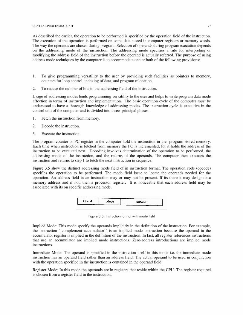
Figure 3.5 show the distinct addressing mode field of in instruction format. The operation code (opcode) specifies the operation to be performed. The mode field issue to locate the operands needed for the operation. An address field in an instruction may or may not be present. If its there it may designate a memory address and if not, then a processor register. It is noticeable that each address field may be associated with its on specific addressing mode.
�
��������,��-�����#��������� �������� �$�����!$�
Implied Mode: This mode specify the operands implicitly in the definition of the instruction. For example, the instruction ‘‘complement accumulator’’ is an implied mode instruction because the operand in the accumulator register is implied in the definition of the instruction. In fact, all register references instructions that use an accumulator are implied mode instructions. Zero-address introductions are implied mode instructions.
Immediate Mode: The operand is specified in the instruction itself in this mode i.e. the immediate mode instruction has an operand field rather than an address field. The actual operand to be used in conjunction with the operation specified in the instruction is contained in the operand field.
Register Mode: In this mode the operands are in registers that reside within the CPU. The register required is chosen from a register field in the instruction.
COMPUTER SYSTEM ARCHITECTURE 78
Register Indirect Mode: In this mode the instruction specifies a register in the CPU that contains the address of the operand and not the operand itself. Usage of register indirect mode instruction necessitates the placing of memory address of the operand in the processor register with a previous instruction.
Autoincrement or Autodecrement Mode: After execution of every instruction from the data in memory it is necessary to increment or decrement the register. This is done by using the increment or decrement instruction. Given upon its sheer necessity some computers use special mode that increments or decrements the content of the registers automatically.
Direct Address Mode: In this mode the operand resides in memory and its address is given directly by the address field of the instruction such that the affective address is equal to the address part of the instruction.
Indirect Address Mode: Unlike direct address mode, in this mode give the address field give the address where the effective address is stored in memory. The instruction from memory is fetched through control to read is address part to access memory again to read the effective address. A few addressing modes require that the address field of the instruction be added to the content of a specific register in the CPU. The effective address in these modes is obtained from the following equation:
effective address = address part of instruction + context of CPU register
The CPU Register used in the computation may be the program counter, Index Register or a base Register.
Relative Address Mode: This mode is applied often with branch type instruction where the branch address position is relative to the address of the instruction word itself. As such in the mode the content of the program counter is added to the address part of the instruction in order to obtain the effective address whose position in memory is relative to the address of the next instruction. Since the relative address can be specified with the smaller number of bits then those required the design the entire memory address, it results in a shorter address field in the instruction format.
Indexed Addressing Mode: In this mode the effective address is obtained by adding the content of an index register to the address part of the instruction. The index register is a special CPU register that contains an index value and can be incremented after its value is used to access the memory.
Base Register Addressing Mode: In this mode the affective address is obtained by adding the content of a base register to the part of the instruction like that of the indexed addressing mode though the register here is a base register and not a index register. The difference between the two modes is based on their usage rather than their computation. An index register is assumed to hold an index number that is relative to the address part of the instruction. A base register is assumed to hold a base address and the address field of the instruction, and gives a displacement relative to this base address. The base register addressing mode is handy for relocation of programs in memory to another as required in multi programming systems. The address values of instruction must reflect this change of position with a base register, the displacement values of instructions do not have to change. Only the value of the base register requires updating to reflect the beginning of a new memory segment.
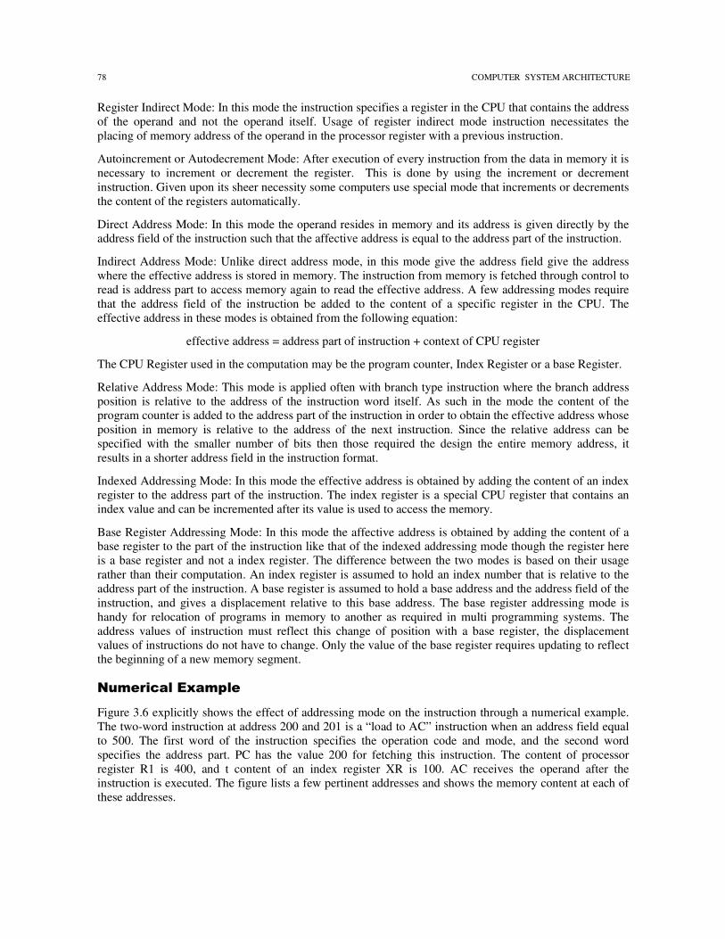
#�� �����$%� &���
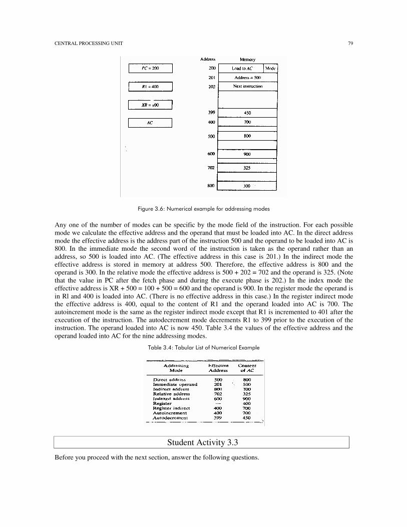
Figure 3.6 explicitly shows the effect of addressing mode on the instruction through a numerical example. The two-word instruction at address 200 and 201 is a “load to AC” instruction when an address field equal to 500. The first word of the instruction specifies the operation code and mode, and the second word specifies the address part. PC has the value 200 for fetching this instruction. The content of processor register R1 is 400, and t content of an index register XR is 100. AC receives the operand after the instruction is executed. The figure lists a few pertinent addresses and shows the memory content at each of these addresses.
CENTRAL PROCESSING UNIT 79
�
��������.��/ �� ���# !��' � �!������ $$��������� �$��������
Any one of the number of modes can be specific by the mode field of the instruction. For each possible mode we calculate the effective address and the operand that must be loaded into AC. In the direct address mode the effective address is the address part of the instruction 500 and the operand to be loaded into AC is 800. In the immediate mode the second word of the instruction is taken as the operand rather than an address, so 500 is loaded into AC. (The effective address in this case is 201.) In the indirect mode the effective address is stored in memory at address 500. Therefore, the effective address is 800 and the operand is 300. In the relative mode the effective address is 500 + 202 = 702 and the operand is 325. (Note that the value in PC after the fetch phase and during the execute phase is 202.) In the index mode the effective address is XR + 500 = 100 + 500 = 600 and the operand is 900. In the register mode the operand is in Rl and 400 is loaded into AC. (There is no effective address in this case.) In the register indirect mode the effective address is 400, equal to the content of R1 and the operand loaded into AC is 700. The autoincrement mode is the same as the register indirect mode except that R1 is incremented to 401 after the execution of the instruction. The autodecrement mode decrements R1 to 399 prior to the execution of the instruction. The operand loaded into AC is now 450. Table 3.4 the values of the effective address and the operand loaded into AC for the nine addressing modes.
� !���(��� �! ����������/ �� ���# !�"' � �!��
�
Student Activity 3.3
Before you proceed with the next section, answer the following questions.
COMPUTER SYSTEM ARCHITECTURE 80
1. What must be the address field of an indexed addressing mode instruction be to make it the same as a register indirect mode instruction?
2. An instruction is stored at location 300 with its address field at location 301. The address field has the value 400. A processor register as contains the number 200. Evaluate the effective address if the addressing mode of the instruction is
(a) Direct (b) Immediate
(c) Relative (d) Register indirect
(e) Index with R1 as the index register
If your answers are correct, then proceed with the next section.
Top
'�����(�����"��&���� ��
Computers are a boon to mankind when its come to carrying out various computational tasks, for they provide an extensive set of instructions to give the user the flexibility to perform these tasks. The basic difference between the instruction set of various computers is the way the operands are determined from the address and mode fields. But there are certain basic operations that are included in the instructions set every computer. Such a basic set of operation available in a typical computer can be classified in the three categories:
1. Data transfer instructions.
2. Data manipulation instructions.
3. Program control instructions.
'�����(���������� ���
As the name suggests data transfer instructions are meant for transfer for data from one location to another, keeping the binary information intact. The useful transfer are between memory and processing registers, between processor registers and input or output, and between the processor registers themselves. Each instruction is accompanied with the mnemonic symbol which are different in different computers for the same instruction name. Table 3.5 gives a list of eight data transfer instructions used in many computers.
The “load” instruction represent a transfer from memory to a processor register, usually an “accumulator” where as the store instruction designates a transfer from a processor register into memory. The move instruction is employed in computers with multiple CPU registers to designate a transfer from one register to another. It has also been used for data transfers between CPU registers and memory or between two memory words. Swapping of information between to registers of a register and memory word its accomplished by using the exchange instruction. The input and output instructions cause transfer of data among processor registers and input or output terminals. The push and pop instructions take care of transfer of data between processor registers and a memory stack.
To distinguish with between the various address modes, the mnemonic symbol are modified by assembly language conventions. For instance, the mnemonic for load immediate becomes LDI. Other assembly language conventions use a special character to designate the addressing mode. For example, the immediate mode is recognized from a pound sign # placed before the operand. What ever may be the case, the important thing is to realize that each instruction can occur with a variety of addressing modes.
� !���,���)��# !�0 � ��� ������-�����#������
CENTRAL PROCESSING UNIT 81
/ � ��� � ��� ���#�
������ ���
����� ���
� � �� � � ��
��������� ����
������� �� �
� ������� � ���
������ �����
�� ��� �� ��
It is imperative to be familiar with the addressing mode used, as well as the type of instructions available in the computer so as to writer assembly language programs for the computer.
'��" ��&���� ���������� ���
Data manipulation instructions are those that perform operations on data and are a help in computation done on computers provide the computational capabilities for the computer.
1. Arithmetic instructions.
2. Logical and bit manipulation instructions.
3. Shift instructions.
�� ����� ��������� ��
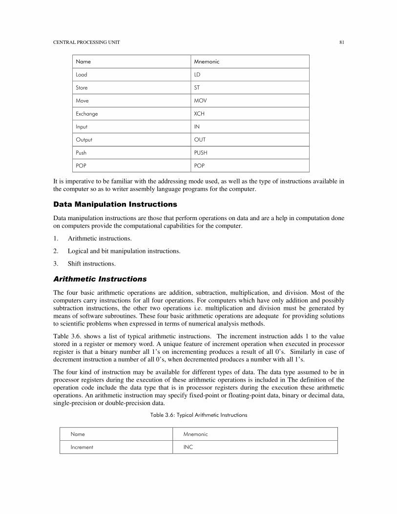
The four basic arithmetic operations are addition, subtraction, multiplication, and division. Most of the computers carry instructions for all four operations. For computers which have only addition and possibly subtraction instructions, the other two operations i.e. multiplication and division must be generated by means of software subroutines. These four basic arithmetic operations are adequate for providing solutions to scientific problems when expressed in terms of numerical analysis methods.
Table 3.6. shows a list of typical arithmetic instructions. The increment instruction adds 1 to the value stored in a register or memory word. A unique feature of increment operation when executed in processor register is that a binary number all 1’s on incrementing produces a result of all 0’s. Similarly in case of decrement instruction a number of all 0’s, when decremented produces a number with all 1’s.
The four kind of instruction may be available for different types of data. The data type assumed to be in processor registers during the execution of these arithmetic operations is included in The definition of the operation code include the data type that is in processor registers during the execution these arithmetic operations. An arithmetic instruction may specify fixed-point or floating-point data, binary or decimal data, single-precision or double-precision data.
� !���.���)��# !������� ���#�-�����#������
�� � � � ��!��
��� ��� ����
COMPUTER SYSTEM ARCHITECTURE 82
�� ��� ����
"��� "���
��#����� ��$�
� �%�!�%&� � ���
�! !�� ����
"���'!�����&� "����
��#�����'!���#��'� ��$$�
� ����()*���� �% ��+� ��, �
The instruction “add with carry” performs the addition on two operands plus the value of the carry from the previous computation. Similarly, the “subtract with borrow” instruction subtracts two words and a borrow which may have resulted from a previous subtract operation. The negate instruction forms the 2’s complement of a number, effectively reversing the sign of an integer when represented in the signed-2’s complement form.
) ��������*���"��&���� ���������� ���
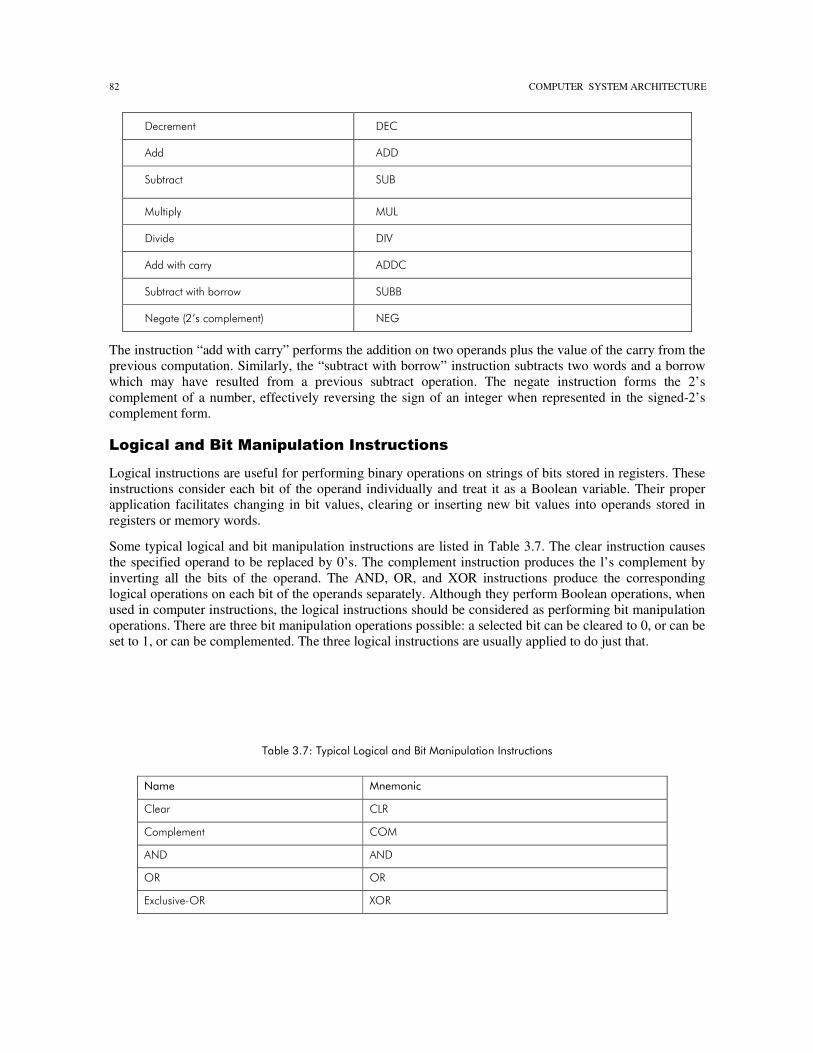
Logical instructions are useful for performing binary operations on strings of bits stored in registers. These instructions consider each bit of the operand individually and treat it as a Boolean variable. Their proper application facilitates changing in bit values, clearing or inserting new bit values into operands stored in registers or memory words.
Some typical logical and bit manipulation instructions are listed in Table 3.7. The clear instruction causes the specified operand to be replaced by 0’s. The complement instruction produces the l’s complement by inverting all the bits of the operand. The AND, OR, and XOR instructions produce the corresponding logical operations on each bit of the operands separately. Although they perform Boolean operations, when used in computer instructions, the logical instructions should be considered as performing bit manipulation operations. There are three bit manipulation operations possible: a selected bit can be cleared to 0, or can be set to 1, or can be complemented. The three logical instructions are usually applied to do just that.
�
�
� !���1���)��# !�����# !� �$�2���� ����! �����-�����#������
/ � ��� � ��� ���#�
�%�� ��-�
�� �% ��� �� � �
"��� "���
� -� � -�
���%��! .� -� �� -�
CENTRAL PROCESSING UNIT 83
�%����&� ��-��
�����&� �����
�� �% �����&� �� � ��
���#%�!������ ���
�!��#%�!������ ���
Individual bits such as a carry can be cleared, set, or complemented with appropriate instructions. Another example that can be cited is of a flip-flop that controls the interrupt facility and is either enabled or disabled by means of bit manipulation instructions.
���(���������� ���
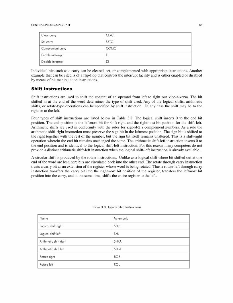
Shift instructions are used to shift the content of an operand from left to right our vice-a-versa. The bit shifted in at the end of the word determines the type of shift used. Any of the logical shifts, arithmetic shifts, or rotate-type operations can be specified by shift instruction. In any case the shift may be to the right or to the left.
Four types of shift instructions are listed below in Table 3.8. The logical shift inserts 0 to the end bit position. The end position is the leftmost bit for shift right and the rightmost bit position for the shift left. Arithmetic shifts are used in conformity with the rules for signed-2’s complement numbers. As a rule the arithmetic shift-right instruction must preserve the sign bit in the leftmost position. The sign bit is shifted to the right together with the rest of the number, but the sign bit itself remains unaltered. This is a shift-right operation wherein the end bit remains unchanged the same. The arithmetic shift-left instruction inserts 0 to the end position and is identical to the logical shift-left instruction. For this reason many computers do not provide a distinct arithmetic shift-left instruction when the logical shift-left instruction is already available.
A circular shift is produced by the rotate instructions. Unlike as a logical shift where bit shifted out at one end of the word are lost, here bits are circulated back into the other end. The rotate through carry instruction treats a carry bit as an extension of the register whose word is being rotated. Thus a rotate-left through carry instruction transfers the carry bit into the rightmost bit position of the register, transfers the leftmost bit position into the carry, and at the same time, shifts the entire register to the left.
�
�
� !���3���)��# !�%�����-�����#������
�� �� � � ��!��
���!��%���!/��!����� ��-�
���!��%���!/��%/��� ����
"!�� �!����!/��!����� ��-"�
"!�� �!����!/��%/��� ���"�
-�����!����� -� -�
-�����%/��� -� ��
COMPUTER SYSTEM ARCHITECTURE 84
-�����!�������������&�� -� -��
-�����%/�����������&�� -� ���
Student Activity 3.4
Before you proceed with the next section, answer the following questions.
1. Given the 16-bit value 10011011001101. What operation must be performed in order to clear to 0 the first eight bits?
2. Distinguish between, Arithmetic shift, logical shift and circular shift operations.
If your answers are correct, then proceed with the next section.
Top
" �� �� �� � ���� �� ��
Memory locations are storage house for instructions. When processed in the CPU, the instructions are fetched from consecutive memory locations and implemented. Each time an instruction is fetched from memory, the program counter is simultaneously incremented with the address of the next instruction in sequence. Once a data transfer or data manipulation instruction is executed, control returns to the fetch cycle with the program counter containing the address of the instruction next in sequence. In case of a program control type of instruction execution of instruction may change the address value in the program counter and cause the flow of control to be altered.
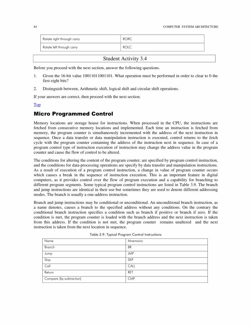
The conditions for altering the content of the program counter, are specified by program control instruction, and the conditions for data-processing operations are specify by data transfer and manipulation instructions. As a result of execution of a program control instruction, a change in value of program counter occurs which causes a break in the sequence of instruction execution. This is an important feature in digital computers, as it provides control over the flow of program execution and a capability for branching to different program segments. Some typical program control instructions are listed in Table 3.9. The branch and jump instructions are identical in their use but sometimes they are used to denote different addressing modes. The branch is usually a one-address instruction.
Branch and jump instructions may be conditional or unconditional. An unconditional branch instruction, as a name denotes, causes a branch to the specified address without any conditions. On the contrary the conditional branch instruction specifies a condition such as branch if positive or branch if zero. If the condition is met, the program counter is loaded with the branch address and the next instruction is taken from this address. If the condition is not met, the program counter remains unaltered and the next instruction is taken from the next location in sequence.
� !���4���)��# !������ � �������!�-�����#�����
�� �� � � ��!��
$������ $-�
0� ��� 0� ��
�1!��� �2��
��%%�� �"���
-����� -���
�� ���(#&���#����!��+�� �� ��
CENTRAL PROCESSING UNIT 85
����(#&�"��!��+�� ����
The skip instruction does not require an address field and is, therefore, a zero-address instruction. A conditional skip instruction will skip the next instruction if the condition is met. This is achieved by incrementing the program counter during the execute phase in addition to its being incremented during the fetch phase. If the condition is not met, control proceeds with the next instruction in sequence where the programmer inserts an unconditional branch instruction. Thus, a skip-branch pair of instructions causes a branch if the condition is not met, while a single conditional branch instruction causes a branch if the condition is met.
The call and return instructions are used in conjunction with subroutines. The compare instruction performs a subtraction between two operands, but the result of the operation is not retained. However, certain status bit conditions are set as a result of the operation. In a similar fashion the test instruction performs the logical AND of two operands and updates certain status bits without retaining the result or changing the operands. The status bits of interest are the carry bit, the sign bit, a zero indication, and an overflow condition.
The four status bits are symbolized by C, S, Z, and V. The bits are set or cleared as a result of an operation performed in the ALU.
1. Bit C (carry) is set to 1 if the end carry C8 is 1 .It is cleared to 0 if the carry is 0.
2. Bit S (sign) is set to 1 if the highest-order bit F7 is 1. It is set to 0 if the bit is 0.
3. Bit Z (zero) is set to 1 if the output of the ALU contains all 0’s. It is cleared to 0 otherwise. In other words, Z = 1 if the output is zero and Z = 0 if the output is not zero.
4. Bit V (overflow) is set to 1 if the exclusive-OR of the last two carries is equal to 1, and cleared to 0 otherwise. This is the condition for an overflow when negative numbers are in 2’s complement. For the 8-bit ALU, V = 1 if the output is greater than +127 or less than -128.
��������1��%� �������������2�����
The status bits can be checked after an ALU operation to determine certain relationships that exist between the values of A and B. If bit V is set after the addition of two signed numbers, it indicates an overflow condition. If Z is set after an exclusive-OR operation, it indicates that A = B. This is so because x � x = 0,
COMPUTER SYSTEM ARCHITECTURE 86
and the exclusive-OR of two equal operands gives an all-0’s result which sets the Z bit. A single bit in A can be checked to determine if it is 0 or 1 by masking all bits except the bit in question and then checking the Z status bit. For example, let A = 101x1100, where x is the bit to be checked. The AND operation of A with B = 00010000 produces a result 000x0000. If x = 0, the Z status bit is set, but if x = I, the Z bit is cleared since the result is not zero.
� ����� ���*������������ ���
The commonly used branch instructions are listed below in Table 3.10. Each mnemonic is constructed with the letter B (for branch) and an abbreviation of the condition name. When the opposite condition state is used, the letter N (for no) is inserted to define the 0 state. Thus BC is Branch on Carry, and BNC is Branch on No Carry. If the stated condition is met, the address specified by the instruction receives program control. If not, control continues with the instruction that follows. The conditional instructions can be associated also with the jump, skip, call, or return type of program control instructions. The zero status bit is employed for testing if the result of an ALU operation is equal to zero or not. The carry bit is employed to check if there is a carry out of the most significant bit position of the ALU. It is also used in conjunction with the rotate instructions to check the bit shifted from the end position of a register into the carry position. The sign bit reflects the state of the most significant bit of the output from the ALU. S = 0 denotes a positive sign and S = 1, a negative sign. Therefore, a branch on plus checks for a sign bit of 0 and a branch on minus checks for a sign bit of 1. It is worth noticeable that these two conditional branch instructions can be used to check the value of the most significant bit whether it represents a sign or not. The overflow bit is used in conjunction with arithmetic operations done on signed numbers in 2's complement representation.
�
�
� !���5�����$����� !�2� �#��-�����#������
�
It has been discussed earlier that the compare instruction performs a subtraction of two operands, say A - B. The result of the operation is not transferred into a destination register, but the status bits are affected. The status register provides Information about the relative magnitude of A and B. Some computers provide
CENTRAL PROCESSING UNIT 87
conditional branch instructions that can be applied right after the execution of a compare instruction. The specific conditions to be tested depend on whether the two numbers A and B are considered to be unsigned or signed numbers.
Consider an 8-bit ALU as shown in Fig. 3.7. The largest unsigned number that can be accommodated in 8 bits is 255. The range of signed numbers is between +127 and -128. The subtraction of two numbers is the same whether they are unsigned or in signed-2's complement representation. Let A = 11110000 and B = 00010100. To perform A -B, the ALU takes the 2's complement of B and adds it to A.
0Z����������0���������V1S����������1���C����������11011100�:BA11101100:1B
11110000��:�����A
====−++
The compare instruction updates the status bits as shown. C = 1 because there is a carry out of the last stage. S = I because the leftmost bit is 1. V = 0 because the last two carries are both equal to 1, and Z = 0 because the result is not equal to 0.
If we assume unsigned numbers, the decimal equivalent of A is 240 and that of B is 20. The subtraction in decimal is 240-20 = 220. The binary result 11011100 is indeed the equivalent of decimal 220. Since 240 > 20, we have that A > B and A f B. These two relations can also be derived from the fact that status bit C is equal to I and bit Z is equal to 0. The instructions that will cause a branch after this comparison are BHI (branch if higher), BHE (branch if higher or equal), and BNE (branch if not equal).
If we assume signed numbers, the decimal equivalent of A is-16. This is because the sign of A is negative and 11110000 is the 2's complement of 00010000, which is the decimal equivalent of +16. The decimal equivalent of B is +20. The subtraction in decimal is (-16) - (+20) = -36. The binary result 11011100 (the 2's complement of 00100100) is indeed the equivalent of decimal -36. Since (-16)< (+20) we have that A< B and A ≠ B. These two relations can also be derived from the fact that status bits S = 1 (negative), V = 0 (no overflow), and Z = 0 (not zero). The instructions that will cause a branch after this comparison are BLT (branch if less than), BLE (branch if less or equal), and BNE (branch if not equal).
It should be noted that the instruction BNE and BNZ (branch if not zero) are identical. Similarly, the two instructions BE (branch if equal) and BZ (branch if zero) are also identical.
��+ �������������������
A subroutine is a self-contained sequence of instructions that does away the computational tasks. A subroutine is employed a number of times during the execution of a program. Wherever a subroutine is called to perform its function, a branch is executed to the beginning of the subroutine to start executing its set of instructions. After the subroutine has been executed, a branch is reverted to the main program.
Various names are assigned to the instruction that transfers program control to a subroutine. For example, call subroutine, jump to subroutine, branch to subroutine do. A call subroutine instruction comprises of an operation code with an address that specifies the beginning of the subroutine. As such two operations are included for execution of instruction (1) storage of the address of next instruction available in the program counter (the return address) in a temporary location so that the subroutine knows where to return, and (2) transfer of control to the beginning of the subroutine. The last instruction of every subroutine, referred as return from subroutine, causes transfer of returns address from the temporary location into the program counter. Consequently, program control is transferred to the instruction whose address was originally stored in the temporary location.
The temporary location for storing the return address differs from one computer to another. Some store it in a fixed location in memory, some store it in the first memory location of the subroutine, some store it in a
COMPUTER SYSTEM ARCHITECTURE 88
processor rights and some store it in a memory stack. However, the best way is to store the return address in a memory stack. This is advantageous when successive subroutines are called because the sequential return addresses can be pushed into the stack. The return from subroutine instruction causes the stack to pop and the contents of the top of the stack are transferred to the program counter.
When a subroutine stack is employed, all return addresses are automatically stored by the hardware in one unit. This does away the problem of recalling where the return address was stored.
� �� ������&��
Program interrupt can be described as a transfer of program control from a currently running program to another service program on a request generated externally or internally. After the service program is executed, the control returns to the original program.
The interrupt procedure is identical to a subroutine call except for three variations: (1) The interrupt is usually generated by an internal or external signal rather than from the execution of an instruction (except for software interrupt); (2) the address of the interrupt service program is determined by the hardware rather than from the address field of an instruction; and (3) an interrupt procedure usually stores all the information necessary to define the state of the CPU rather than storing only the program counter.
It is imperative for the CPU to return to the same state that it was when interrupt occurred after the program interrupted and the service routine has been executed. The state of the CPU at the end of the execute cycle (when the interrupt is recognized) is determined from:
1. The content of the program counter.
2. The content of all processor registers.
3. The content of certain status conditions.
The collection of all status bit conditions in the CPU is referred as a program status word or PSW. The PSW is stored in a separate hardware register and contains the status information that characterizes the state of the CPU. It is inclusive of the status bits from the last ALU operation and specifies the interrupts that are allowed to occur and whether the CPU is operating in a supervisor or user mode. Most of the computers have a resident operating system that controls and supervises all other programs in the computer. When the CPU is executives a program that is part of the operating system, it is referred to be in the supervisor or system mode. Certain instructions are executed in this mode only. The CPU is normally in the user mode when user programs are executed. Special status bits in the PSW determine the mode advantage the CPU is operating at any given time.
In certain computers only the program counter is stored when responding to an interrupt. The service program must then include instructions to store status and register content before these resources are used. Very few computers store both program counter and all status and register content in response to an interrupt. Most computers store the program counter and the PSW only. Some computers may have two sets of processor registers within the computer, one for each CPU mode. In this way, when the program switches from the user to the supervisor mode (or vice versa) in response to an interrupt, storing the contents of processor registers is not required as each mode uses its own set of registers.
The hardware procedure for processing an interrupt is very similar to the execution of a subroutine call instruction.
�,&��� (������&���
CENTRAL PROCESSING UNIT 89
Interrupts can be classified into the major types as given below:
1. External interrupts
2. Internal interrupts
3. Software interrupts
External interrupts come from input-output (I/O) devices, from a timing device, from a circuit monitoring the power supply, or from any other external source. Various examples that cause external interrupts are I/O device requesting transfer of data, I/O device finished transfer of data, elapsed time of an event, or power failure. Time-out interrupt may result from a program that is in an endless loop and thus consumes more time its time allocation. Power failure interrupt may have as its service routine a program that transfers the complete state of the CPU into a nondestructive memory in the few milliseconds before power ceases.
Internal interrupts arise when an instruction or data is used illegally or erroneously. These interrupts are also known as traps. Examples of interrupts caused by internal error conditions are register overflow, attempt to divide by zero, an invalid operation code, stack overflow, and protection violation. Occurrence of internal errors is usually a resultant of a premature termination of the instruction execution. Remedial majors to be taken are again determine by service program that processors the internal interrupts.
To distinguish between internal and external interrupts, the internal interrupt is generated by some exceptional condition caused by the program itself rather than by an external event. Internal interrupts are synchronous with the program while external interrupts are asynchronous. On rerunning of the program, the internal interrupts will occur in exactly same place each time. On the contrary external interrupts being dependent on external conditions, are independent of the program being executed at the time.
External and internal interrupts are generated from signals that occur in the hardware of the CPU. On the contrary, a software interrupt is initiated during execution of an instruction. In precise terms, software interrupt is a special call instruction that behaves like an interrupt rather than a subroutine call. It can be called to function by the programmer to initiate an interrupt procedure at any desired point in the program. Usages of software interrupt is mostly associated with a supervisor call instruction. This instruction is meant for switching from a CPU user mode to the supervisor mode. Certain operations in the computer are privileged to be assigned to the supervisor mode only, as for example, a complex input or output transfer procedure. A program written by a user must run in the user mode. When an input or output transfer is required, the request for the supervisor mode is sent by means of a supervisor call instruction. This instruction causes a software interrupt that stores the old CPU state and brings in a new PSW that belongs to the supervisor mode. This information must be passed to the operating system from the calling program so as to specify the particular task requested.
Student Activity 3.5
Before you proceed with the next section, answer the following questions.
1. What are the differences between a branch instructions, a call subroutine instruction, and program interrupt?
2. Give five examples of external interrupts and five examples of internal interrupts.
3. What is the difference between a software interrupt and a subroutine call?
If your answers are correct, then proceed with the next section.
Top
���������������� ������� � &����
COMPUTER SYSTEM ARCHITECTURE 90
The design of the instruction set for the processor is very important in terms of computer architecture. It’s the instruction set of a particular computer that determines the way that machine language programs are constructed. Computer hardware is improvised by various factors, such as upgrading existing models to provide more customer applications adding instructions that facilitate the translation from high-level language into machine language programs and striving to develop machines that move functions from software implementation into hardware implementation. A computer with a large number of instructions is classified as a complex instruction set computer, abbreviated as CISC.
In the developing years, computers designer felt the needs of computers that use fewer instructions with simple constructs so they can be executed much faster within the CPU without having to use memory as often. This type of computer is classified as a reduced instruction set computer or RISC. The design of an instruction set for a computer depends on not only machine language constructs, but also on the requirements imposed on the use of high-level programming languages. A compiler program translate high level languages to machine language programs. The basic reason to a design a complex instruction set is the need to simplify the compilation and enhance the overall computer efficiency. The essential goal of a CISC architecture is to attempt to provide a single machine instruction for each statement that is written in a high-level language.
�����������������
The essential goal of RISC architecture involves an attempt to reduce execution time by simplifying the instruction set of the computer. The major characteristics of a RISC processor are:
� Relatively few instructions.
� Relatively few addressing modes.
� Memory access limited to load and store instructions.
� All operations done within the registers of the CPU.
� Fixed length easily decoded instruction format.
� Single-cycle instruction execution.
� Hardwired rather than microprogrammed control.
A typical RISC processor architecture includes register-to-register operations, with only simple load and store operations for memory access. Thus the operand is code into a processor register with a load instruction. All computational tasks are performed among the data stored in processor registers and with the help of store instructions results are transferred to the memory. This architectural feature simplifies the instruction set and encourages the optimization of register manipulation. Almost all instructions have simple register addressing so only a few addressing modes are utilised. Other addressing modes may be included, such as immediate operands and relative mode. An advantage of RISC instruction format is that it is easy to decode.
An important feature of RISC processor is its ability to execute one instruction per clock cycle. This is done by a procedure referred to as pipelining. A load or store instruction may need two clock cycles because access to memory consumes more time than register operations. Other characteristics attributed to RISC architecture are:
� A relatively large number of register in the processor unit.
� Use of overlapped register windows to speed-up procedure call and return.
� Efficient instruction pipeline.
CENTRAL PROCESSING UNIT 91
� Compiler support for efficient translation of high-level language programs into machine language programs.
Student Activity 3.6
Before you proceed with the next section, answer the following questions.
1. What does RISC stand for?
2. What does CISC stand for?
3. What are the characteristics of RISC?
4. What are the characteristics of CISC?
If your answers are correct, then proceed with the next section.
Top
������� ��������
Parallel processing denotes a large class of techniques that are used to deliver simultaneous data-processing tasks to enhance the computational speed of a computer system. A parallel processing system performs concurrent data processing to achieve faster execution time unlike the conventional computer where in each instruction is processed sequentially. For example, while an instruction is being executed in the ALU, the next instruction can execute two or more instructions at the same time. Furthermore, the system may have two or more processors operating concurrently. The goal of parallel processing is anciently to speed up the computer processing capability and increase it throughout, that is, the amount of processing that can be achieved during a given interval of time. Parallel processing, demands for an increase in hardware and that raises the cost of the system. However, technological developments have cut down hardware costs to the level where parallel processing techniques have become economical.
Complexity of parallel processing can be separated at various levels. At the lowest level, we distinguish between parallel and serial operations by the type of registers used. Shift registers operate serially one bit at a time, while registers with parallel load operate with all the bits of the word simultaneously. Parallel processing at a higher level of complexity can be achieved by having multiple functional units that perform identical or different operations at the same time. Parallel processing is established by distributing the data among the multiple functional units. For example, the arithmetic logic, and shift operations can be separated into three units and the operands diverted to each unit under the supervision of a control unit.
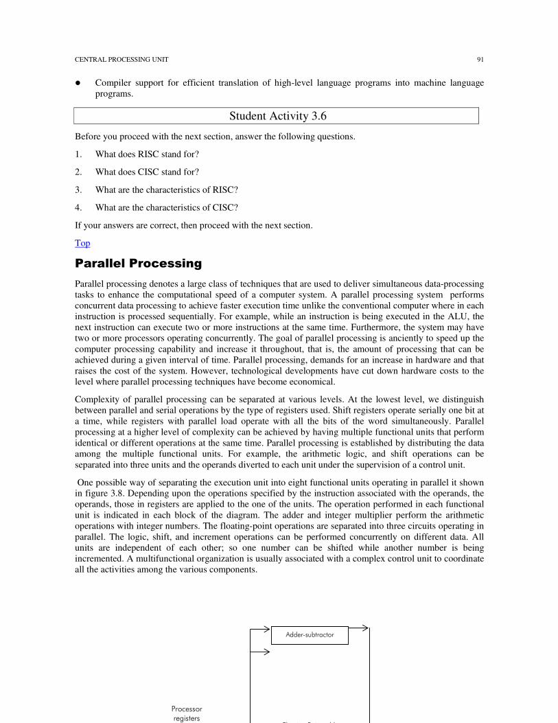
One possible way of separating the execution unit into eight functional units operating in parallel it shown in figure 3.8. Depending upon the operations specified by the instruction associated with the operands, the operands, those in registers are applied to the one of the units. The operation performed in each functional unit is indicated in each block of the diagram. The adder and integer multiplier perform the arithmetic operations with integer numbers. The floating-point operations are separated into three circuits operating in parallel. The logic, shift, and increment operations can be performed concurrently on different data. All units are independent of each other; so one number can be shifted while another number is being incremented. A multifunctional organization is usually associated with a complex control unit to coordinate all the activities among the various components.
�
�
�
� "��.��#������
3%���!�����!������.
��������!����
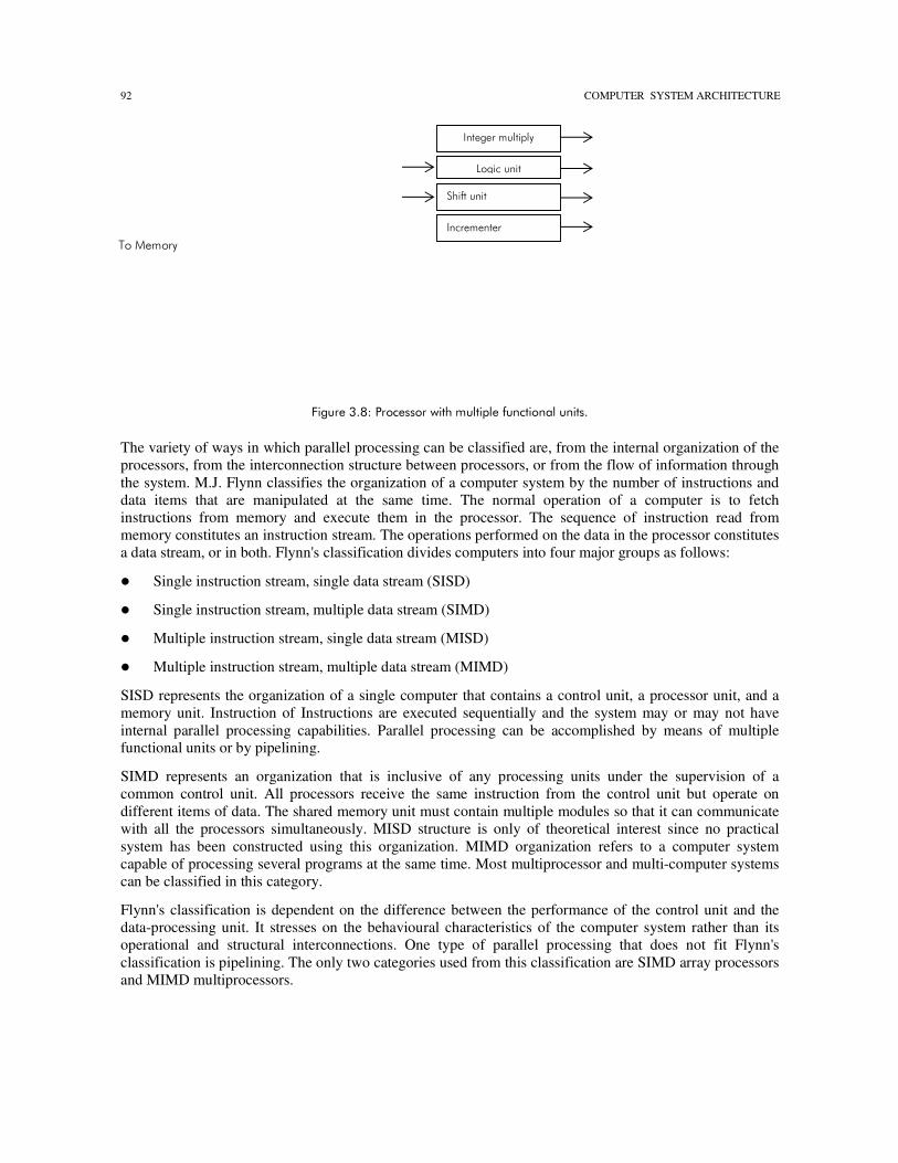
COMPUTER SYSTEM ARCHITECTURE 92
��������3�����#������������ �!���!�����#���� !�������
The variety of ways in which parallel processing can be classified are, from the internal organization of the processors, from the interconnection structure between processors, or from the flow of information through the system. M.J. Flynn classifies the organization of a computer system by the number of instructions and data items that are manipulated at the same time. The normal operation of a computer is to fetch instructions from memory and execute them in the processor. The sequence of instruction read from memory constitutes an instruction stream. The operations performed on the data in the processor constitutes a data stream, or in both. Flynn's classification divides computers into four major groups as follows:
� Single instruction stream, single data stream (SISD)
� Single instruction stream, multiple data stream (SIMD)
� Multiple instruction stream, single data stream (MISD)
� Multiple instruction stream, multiple data stream (MIMD)
SISD represents the organization of a single computer that contains a control unit, a processor unit, and a memory unit. Instruction of Instructions are executed sequentially and the system may or may not have internal parallel processing capabilities. Parallel processing can be accomplished by means of multiple functional units or by pipelining.
SIMD represents an organization that is inclusive of any processing units under the supervision of a common control unit. All processors receive the same instruction from the control unit but operate on different items of data. The shared memory unit must contain multiple modules so that it can communicate with all the processors simultaneously. MISD structure is only of theoretical interest since no practical system has been constructed using this organization. MIMD organization refers to a computer system capable of processing several programs at the same time. Most multiprocessor and multi-computer systems can be classified in this category.
Flynn's classification is dependent on the difference between the performance of the control unit and the data-processing unit. It stresses on the behavioural characteristics of the computer system rather than its operational and structural interconnections. One type of parallel processing that does not fit Flynn's classification is pipelining. The only two categories used from this classification are SIMD array processors and MIMD multiprocessors.
����� �%�!�%&�
���!����!��
��!/����!��
��� ���
���� �&�
CENTRAL PROCESSING UNIT 93
A parallel processing system performs concurrent data processing to reduce execution time. For instance, while an instruction is being executed in the ALU, the next instruction can be read from memory. The system can execute two or more instructions simultaneous by dent of two or more ALUs in the system. Furthermore, the system may have two or more processors operating concurrently.
There are a numerous ways that parallel processing can be performed. We consider parallel processing under the following main topics:
1. Pipeline processing
2. Vector processing
3. Array processing
Top
��&��������
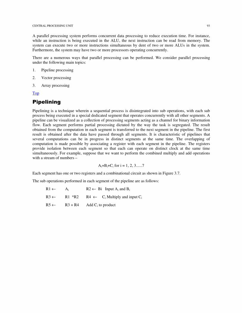
Pipelining is a technique wherein a sequential process is disintegrated into sub operations, with each sub process being executed in a special dedicated segment that operates concurrently with all other segments. A pipeline can be visualized as a collection of processing segments acting as a channel for binary information flow. Each segment performs partial processing dictated by the way the task is segregated. The result obtained from the computation in each segment is transferred to the next segment in the pipeline. The first result is obtained after the data have passed through all segments. It is characteristic of pipelines that several computations can be in progress in distinct segments at the same time. The overlapping of computation is made possible by associating a register with each segment in the pipeline. The registers provide isolation between each segment so that each can operate on distinct clock at the same time simultaneously. For example, suppose that we want to perform the combined multiply and add operations with a stream of numbers –
Ai+Bi+Ci for i = 1, 2, 3......7
Each segment has one or two registers and a combinational circuit as shown in Figure 3.7.
The sub operations performed in each segment of the pipeline are as follows:
R1 ← Ai R2 ← Bi Input Ai and Bi
R3 ← R1 *R2 R4 ← Ci Multiply and input Ci
R5 ← R3 + R4 Add Ci to product
COMPUTER SYSTEM ARCHITECTURE 94
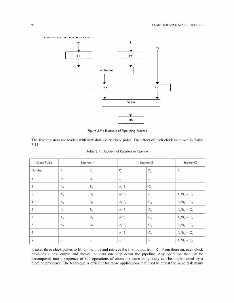
��������4���"' � �!���������!���������#�����
The five registers are loaded with new data every clock pulse. The effect of each clock is shown in Table 3.11.
� !���������������������������������!����
�%��1���%�� �� ���4� �� ��)� �� ��5�
�� #� -4� -
)�-5� -
6� -
7�
4� "4� $4� 8� 8� 8�
)� ")� $)� "49$4� �4� �
5� "5� $5� ")9$)� ��� "49$4�: ��4�
6� "6� $6� "59$5� �5� ")9$)�: ��)�
7� "7� $7� "69$6� �6� "59$5�: ��5�
;� ";� $;� "79$7� �7� "69$6�: ��6�
<� "<� $<� ";9$;� �;� "79$;�: ��7�
=� 8� 8� "<9$<� �<� ";9$;�: ��;�
>� 8� 8� 8� 8� "<9$<�: ��<�
It takes three clock pulses to fill up the pipe and retrieve the first output from R5. From there on, each clock produces a new output and moves the data one step down the pipeline. Any operation that can be decomposed into a sequence of sub operations of about the same complexity can be implemented by a pipeline processor. The technique is efficient for those applications that need to repeat the same task many
CENTRAL PROCESSING UNIT 95
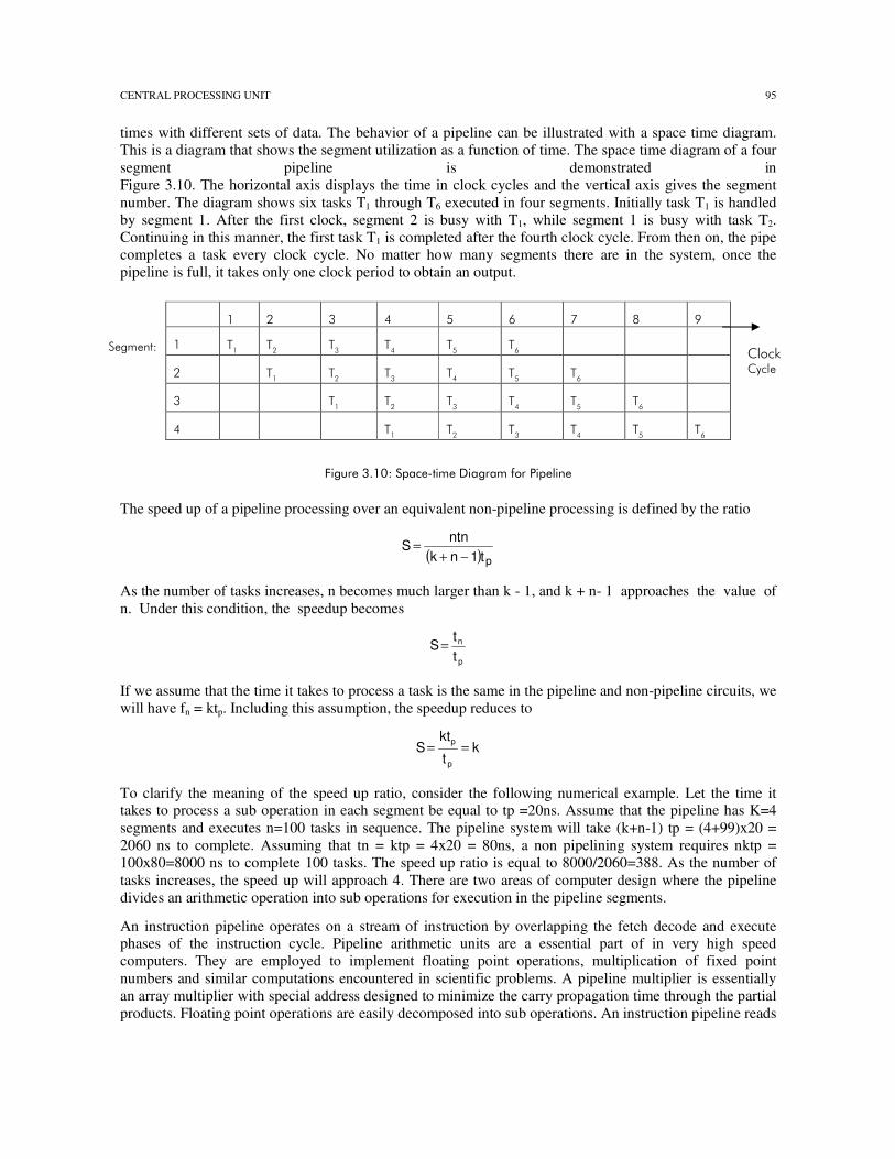
times with different sets of data. The behavior of a pipeline can be illustrated with a space time diagram. This is a diagram that shows the segment utilization as a function of time. The space time diagram of a four segment pipeline is demonstrated in Figure 3.10. The horizontal axis displays the time in clock cycles and the vertical axis gives the segment number. The diagram shows six tasks T1 through T6 executed in four segments. Initially task T1 is handled by segment 1. After the first clock, segment 2 is busy with T1, while segment 1 is busy with task T2. Continuing in this manner, the first task T1 is completed after the fourth clock cycle. From then on, the pipe completes a task every clock cycle. No matter how many segments there are in the system, once the pipeline is full, it takes only one clock period to obtain an output.
� 4� )� 5� 6� 7� ;� <� =� >�
4� �4� �
)� �
5� �
6� �
7� �
;� � � �
)� � �4� �
)� �
5� �
6� �
7� �
;� � �
5� � � �4� �
)� �
5� �
6� �
7� �
;� �
6� � � � �4� �
)� �
5� �
6� �
7� �
;�
��������5��%� #�6��� ��0� �� � ���������!�����
The speed up of a pipeline processing over an equivalent non-pipeline processing is defined by the ratio
( ) pt1nkntn
S−+
=
As the number of tasks increases, n becomes much larger than k - 1, and k + n- 1 approaches the value of n. Under this condition, the speedup becomes
p
n
tt
S =
If we assume that the time it takes to process a task is the same in the pipeline and non-pipeline circuits, we will have fn = ktp. Including this assumption, the speedup reduces to
kt
ktS
p
p ==
To clarify the meaning of the speed up ratio, consider the following numerical example. Let the time it takes to process a sub operation in each segment be equal to tp =20ns. Assume that the pipeline has K=4 segments and executes n=100 tasks in sequence. The pipeline system will take (k+n-1) tp = (4+99)x20 = 2060 ns to complete. Assuming that tn = ktp = 4x20 = 80ns, a non pipelining system requires nktp = 100x80=8000 ns to complete 100 tasks. The speed up ratio is equal to 8000/2060=388. As the number of tasks increases, the speed up will approach 4. There are two areas of computer design where the pipeline divides an arithmetic operation into sub operations for execution in the pipeline segments.
An instruction pipeline operates on a stream of instruction by overlapping the fetch decode and execute phases of the instruction cycle. Pipeline arithmetic units are a essential part of in very high speed computers. They are employed to implement floating point operations, multiplication of fixed point numbers and similar computations encountered in scientific problems. A pipeline multiplier is essentially an array multiplier with special address designed to minimize the carry propagation time through the partial products. Floating point operations are easily decomposed into sub operations. An instruction pipeline reads
�%��1��&�%�
�� ��?�
COMPUTER SYSTEM ARCHITECTURE 96
consecutive instruction from the memory while previous instructions are being executed in other segments. This causes the instruction and execute phases to overlap and perform simultaneous operations. One possible digression associated with such a scheme is that an instruction may cause a branch out of sequence. In that case the pipeline must be emptied and all the instructions that have been read from memory after the branch instruction must be discarded. The instruction fetch segment can be implemented by means of a first-in first-out (FIFO) buffer. This is a type of unit that forms a queue rather than a stack. The design of an instruction pipeline will be most efficient if the instruction cycle is divided into segments of equal duration. The time that each step takes to fulfil its function depends on the instruction and the way it is executed.
Top
����� �������&������
As describe in the previous passage arithmetic pipelines are employed to implement floating-point operations, multiplication of fixed-point numbers, and similar computations encountered in scientific problems. A pipeline multiplier is essentially an array multiplier with special adders designed to minimize the carry propagation time through the partial products. Floating-point operations are easily decomposed into suboperations. We will now show an example of a pipeline unit for floating-point addition and subtraction.
The inputs to the floating-point adder pipeline are two normalized floating-point binary numbers.
X = A × 2a
Y = B × 2b
A and B are two fractions that represent the mantissas and a and b are the exponents. The floating-point addition and subtraction can be performed in four segments, as shown in Fig. 3.11. The registers labeled R are placed between the segments to store intermediate results. The suboperations that are performed in the four segments are:
1. Compare the exponents.
2. Align the mantissas.
3. Add or subtract the mantissas.
4. Normalize the result.
The following numerical example may clarify the suboperations performed in each segment. For simplicity, we use decimal numbers, although Fig. 3.11 refers to binary numbers. Consider the two normalized floating-point numbers:
X = 0.9504 × 10³
Y = 0.8200 × 10³
The two exponents are subtracted in the first segment to obtain 3 -2 = 1. The larger exponent 3 is chosen as the exponent of the result. The next segment shifts the mantissa of Y to the right to obtain
X = 0.9504 × 10³
y = 0.0820 × 10³
This aligns the two mantissas under the same exponent. The addition of the two mantissas in segment 3 produces the sum
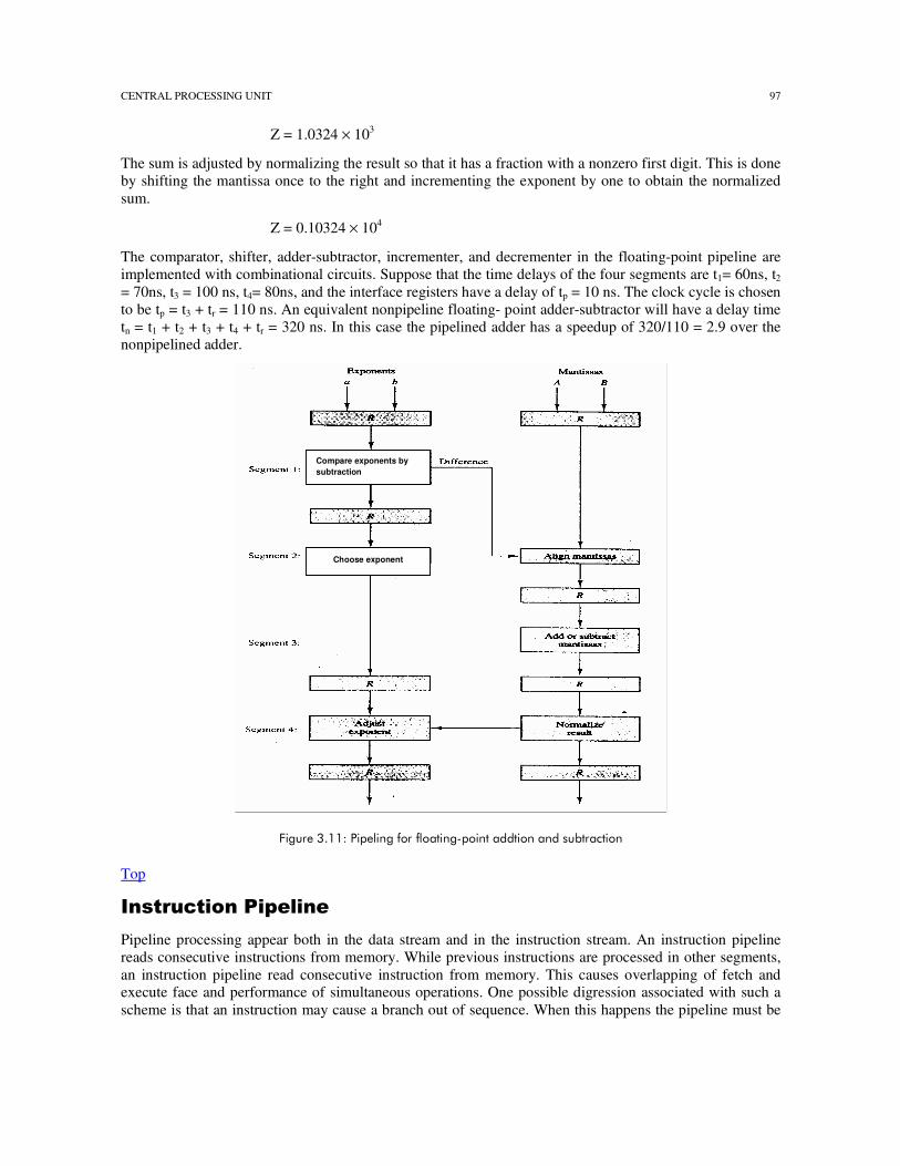
CENTRAL PROCESSING UNIT 97
Z = 1.0324 × 10³
The sum is adjusted by normalizing the result so that it has a fraction with a nonzero first digit. This is done by shifting the mantissa once to the right and incrementing the exponent by one to obtain the normalized sum.
Z = 0.10324 × 10⁴
The comparator, shifter, adder-subtractor, incrementer, and decrementer in the floating-point pipeline are implemented with combinational circuits. Suppose that the time delays of the four segments are t1= 60ns, t2 = 70ns, t3 = 100 ns, t4= 80ns, and the interface registers have a delay of tp = 10 ns. The clock cycle is chosen to be tp = t3 + tr = 110 ns. An equivalent nonpipeline floating- point adder-subtractor will have a delay time tn = t1 + t2 + t3 + t4 + tr = 320 ns. In this case the pipelined adder has a speedup of 320/110 = 2.9 over the nonpipelined adder.
�
��������������!���������!� ����6������ $$����� �$��� �� #�����
Top
�������� ����&������
Pipeline processing appear both in the data stream and in the instruction stream. An instruction pipeline reads consecutive instructions from memory. While previous instructions are processed in other segments, an instruction pipeline read consecutive instruction from memory. This causes overlapping of fetch and execute face and performance of simultaneous operations. One possible digression associated with such a scheme is that an instruction may cause a branch out of sequence. When this happens the pipeline must be
Compare exponents by subtraction
Choose exponent
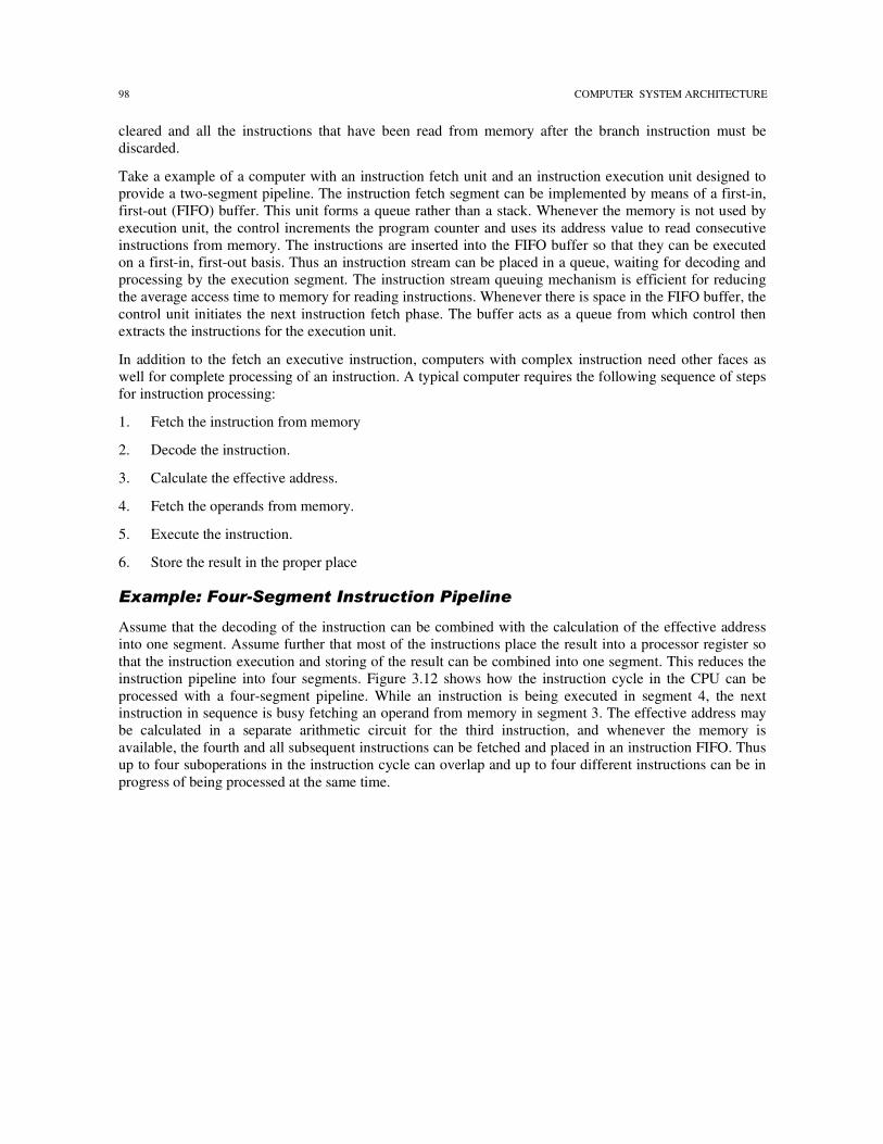
COMPUTER SYSTEM ARCHITECTURE 98
cleared and all the instructions that have been read from memory after the branch instruction must be discarded.
Take a example of a computer with an instruction fetch unit and an instruction execution unit designed to provide a two-segment pipeline. The instruction fetch segment can be implemented by means of a first-in, first-out (FIFO) buffer. This unit forms a queue rather than a stack. Whenever the memory is not used by execution unit, the control increments the program counter and uses its address value to read consecutive instructions from memory. The instructions are inserted into the FIFO buffer so that they can be executed on a first-in, first-out basis. Thus an instruction stream can be placed in a queue, waiting for decoding and processing by the execution segment. The instruction stream queuing mechanism is efficient for reducing the average access time to memory for reading instructions. Whenever there is space in the FIFO buffer, the control unit initiates the next instruction fetch phase. The buffer acts as a queue from which control then extracts the instructions for the execution unit.
In addition to the fetch an executive instruction, computers with complex instruction need other faces as well for complete processing of an instruction. A typical computer requires the following sequence of steps for instruction processing:
1. Fetch the instruction from memory
2. Decode the instruction.
3. Calculate the effective address.
4. Fetch the operands from memory.
5. Execute the instruction.
6. Store the result in the proper place
��������������������������� � ��� ��
Assume that the decoding of the instruction can be combined with the calculation of the effective address into one segment. Assume further that most of the instructions place the result into a processor register so that the instruction execution and storing of the result can be combined into one segment. This reduces the instruction pipeline into four segments. Figure 3.12 shows how the instruction cycle in the CPU can be processed with a four-segment pipeline. While an instruction is being executed in segment 4, the next instruction in sequence is busy fetching an operand from memory in segment 3. The effective address may be calculated in a separate arithmetic circuit for the third instruction, and whenever the memory is available, the fourth and all subsequent instructions can be fetched and placed in an instruction FIFO. Thus up to four suboperations in the instruction cycle can overlap and up to four different instructions can be in progress of being processed at the same time.
CENTRAL PROCESSING UNIT 99
�
����������
Sometimes an instruction in the sequence may be a program control type that causes a branch out of normal sequence. In that case the pending operations in the last two segments are completed and all information stored in the instruction buffer is discards. The pipeline then initiates from the new address stored in the program counter. Similarly, an interrupt request, when acknowledged, will cause the pipeline to empty and start again from a new address value.
Top
�������&������
The reduced instruction set computer (RISC) was introduced earlier in this unit. One of the unique features of risk RISC is its ability to implement an instruction pipeline using a small number of suboperations, with each being executed in one clock cycle. Because of the fixed-length instruction format, the decoding of the operation can occur with the register selection simultaneously. All data manipulation instructions have register-to-register operations. Since all operands are in registers, the need for calculating an effective address or fetching of operands from memory does not arise. The instruction pipeline can be implemented with two or three segments. One segment fetches the instruction from program memory, and the other segment executes the instruction in the ALU. A third segment may be used to store the result of the ALU operation in a destination register.
The data transfer instructions in RISC are limited to load and store instructions. These instructions use register indirect addressing and required three or four stages in the pipeline. To prevent conflicts between a memory access to fetch an instruction and to load or store an operand, Most RISC machines use two separate buses with two memories: one for storing the instructions and the other for storing the data to avoid conflict between memory access to fetch instruction and to load or store an operand. The two memories can have operational speed as that of a CPU clock and are referred to as cache memories.
COMPUTER SYSTEM ARCHITECTURE 100
RISC system is of great benefits in terms of its ability to execute instructions at the rate of one per clock cycle. Practically it does not happen that every instruction can be fetched from memory and executed in one clock cycle. What is done, in effect, is to start each instruction with each clock cycle and to pipeline the processor to achieve the goal of single-cycle instruction execution. The advantage of RISC over CISC (complex instruction set computer) is that RISC can achieve pipeline segments, requiring just one clock cycle, while CISC uses many segments in its pipeline, with the longest segment requiring two or more clock cycles.
RISC system also has a advantage of the support given by the compiler that interprets the high-level language program into machine language program. RISC processors rely heavily on the efficiency of the compiler to detect and minimize the delays encountered with problems associated with data complex and branch penalties .
The following examples show how a compiler can optimize the machine language program to compensate for pipeline conflicts.
��������!�������������������� � ��� ��
The data manipulation instructions operate on data in processor registers. The data transfer instructions are load and store instructions that use an effective address obtained from the addition of the contents of two registers or a register and a displacement constant provided in the instruction. The program control instructions use register values and a constant to evaluate the branch address, which is transferred to a register or the program counter PC.
Now consider the hardware operation for such a computer. The control section fetches the instruction from program memory into an instruction register. The instruction is decoded with the simultaneous selection of registers required for the executive of the instruction. The processor unit consists of a number of registers and an arithmetic logic unit (ALU) that performs the necessary arithmetic, logic, and shift operations. A data memory is used to load or store the data from a selected register in the register file. The instruction cycle can be divided into three suboperations and implemented in three segments:
I: Instruction fetch
A: ALU operation
E: Execute instruction
The I segment fetches the instruction from program memory. The instruction is decoded and an ALU operation is performed in the A segment. The ALU is used for three different functions, depending on the decoded instruction.
It performs an operation for a data manipulation instruction, it evaluates the effective address for a load or store instruction, or it calculates the branch address for a program control instruction. The E segment directs the output of the ALU to one of three destinations, depending on the decoded instruction. It transfers the result of the ALU operation into a destination register in the register file, it transfers the effective address to a data memory for loading or storing, or it transfers the branch address to the program counter.
"������#��
Consider now the operation of the following four instructions:
1. LOAD: R1 ← M[address1]
CENTRAL PROCESSING UNIT 101
2. LOAD: R2 ← M[address2]
3. ADD: R3 ← R1+R2
4. STORE: M[address3] ← R3
�
����������������6���� ��������!������� ����
If the three-segment pipeline proceeds without interruptions, there will be a data conflict in instruction 3 because the operand in R2 is not yet available in the A segment. This can be seen from the timing of the pipeline shown in Fig. 3.13(a). The E segment in clock cycle 4 is in a process of placing the memory data into R2. The A segment in clock cycle 4 is using the data from R2, but the value in R2 will not be the correct value since it has not yet been transferred from memory. It is up to the compiler to make sure that the instruction following the load instruction uses the data fetched from memory. If the compiler cannot find a useful instruction to put after the load, it inserts a no-op (no-operation) instruction. This is a type of instruction that is fetched from memory but has no operation, thus wastes a clock cycle. This concept of delaying thereof the data loaded from memory is referred to as delayed load.
Figure 3.13(b) shows the same program with a no-op instruction inserted after the load to R2 instruction. The data is loaded into R2 in clock cycle 4. The add instruction uses the value of R2 in step 5. Thus the no-op instruction is used to advance one clock cycle in order to compensate for the data conflict in the pipeline. (Note that no operation is performed in segment A during clock cycle 4 or segment E during clock cycle 5.) The advantage of the delayed load approach is that the data dependency is taken care of by the compiler rather than the hardware. This results in a simpler hardware segment since the segment does not have to check if the content of the register being accessed is currently valid or not.
"������$�����
Fig. 3.12 explicitly shows that a branch instruction delays the pipeline operation until the instruction at the branch address is fetched. Several techniques for reducing branch penalties were discussed in the preceding section. The method used in most RISC processors is to rely on the compiler to redefine the branches so that they take effect at the proper time in the pipeline. This method is known as delayed branch.
Top
COMPUTER SYSTEM ARCHITECTURE 102
-��� �� ��������
There are certain computational problems that can not be resolved by a are beyond the capabilities of a conventional computer on the basis of the fact that they require a vast number of computations that will take a conventional computer days or even weeks to complete. In many science and engineering applications, the problems can be formulated in terms of vectors and matrices that tend themselves to vector processing. Computers with vector processing capabilities are very much required in specialized applications. The following are representative application areas where vector processing is of the utmost importance:
� Long-range weather forecasting
� Petroleum explorations
� Seismic data analysis
� Medical diagnosis
� Aerodynamics and space flight simulations
� Artificial intelligence and expert systems
� Mapping the human genome
� Image processing
Vector and parallel processing techniques should be applied to achieve result of high performance in case of unavailability of complex computers to speed up the execution time of instructions.
Many scientific problems require arithmetic operations on large arrays of numbers. These numbers are usually formulated as vectors and matrices of relating point numbers. To examine the difference between a conventional scalar processor and a vector processor, consider the following Fortan Do loop:
DO 20 I = 1, 100
20: C (I) = B(I) + A (I)
This is a program for adding two vectors A and B of length 100 produces a vector C.
This is implemented in machine language by the following sequence of operations:
Initialize I = 0
20 Read A (I)
Read B (I)
Store C (I) = A(I) +B (I)
Increment I = I +1
If I < 100 go to 20 continue
This constitutes a program loop that reaches a pair of operations from arrays A and B and perform a floating point addition. The loop control variable is then updated and the steps repeat 100 times.
A computer capable of vector processing eliminates the overheads associated with the time it takes to fetch and execute the instruction in the program loop. It allows operations to be specified with a single vector instructions of the form
CENTRAL PROCESSING UNIT 103
C (1:100) = A (1: 100) +B (1: 100)
The vector instructions include the initial address of the operands, the length of the vectors and the operation to be performed, all in one composite instruction. The addition is done with a pipelined floating point adder. A possible instruction format for a vector instructions is shown Figure 3.14.
�
��� ���!�������������
�
$��������������4�
�
$��������������)�
�
$������������!���!���
�
�����%�����
��������(�
This is essentially a three address instruction with three fields specifying the base address of the operands and an additional field that gives the length of the data items in the vectors.
�������
Matrix Multiplication
Matrix multiplication is one of the most computational intensive operations performed in computers with vector processors. The multiplication of two n x n matrices consists of n2 inner products or n3 multiply-add operations. An n x m matrix of numbers has n rows and m columns and may be considered as constituting a set of n row vectors or a set of m column vectors. Consider, for example, the multiplication of two 3 x 3 matrices A and B.
The product matrix C is a 3 x 3 matrix whose elements are related to the elements of A and B by the inner product:
kj
3
1kikij baC �
=×=
For example, the number in the first row and first column of matrix C is calculated by letting i = 1, j = 1, to obtain
C11 = a11 b11 + a12 b21 + a13 b31
This requires three multiplications and (after initializing c11 to 0) three additions. The total number of multiplications or additions required to compute the matrix product is 9 x 3= 27. If we consider the linked multiply-add operation c = a x b as a cumulative operation, the product of two n x n matrices requires n2 multiply-add operations. The computation consists of n2 inner products, with each inner product requiring n multiply-add operations, assuming that c is initialized to zero before computing each element in the product matrix.
In general, the inner product consists of the sum of k product terms of the form
C = A1B1 + A2 B2 + A3 + B3 + A4 + B4 + … + Ak Bk
COMPUTER SYSTEM ARCHITECTURE 104
In a typical application k may be equal to 100 or even 1000. The inner product calculation on a pipeline vector processor is shown in Fig. 3.15. The values of A and B are either in memory or in processor registers. The floating-point multiplier pipeline and the floating-point adder pipeline are assumed to have four segments each. All segment registers in the multiplier and adder are initialized to 0. Therefore, the output of the adder is 0 for the first eight cycles until both pipes are full. Ai and Bi pairs are brought in and-multiplied at a rate of one pair per cycle. After the first four cycles, the products begin to be added to the output of the adder. During the next four cycles 0 is added to the products entering the adder pipeline. At the end of the eighth cycle, the first four products A1 B1 through A4 B4 are in the four adder segments, and the next four products, A5B5 through A8 E8 are in the multiplier segments. At the beginning of the ninth cycle, the output of the adder is A1B1 and the output of the multiplier is A5 B5. Thus the ninth cycle starts the addition A1 B1 + A5 B5 in the adder pipeline. The tenth cycle starts the addition A2 B2 + A6 B6, and so on. This pattern breaks down the summation into four sections as follows:
�
��������,������!��������# !#�! ����� �����������$�#��
Top
�,�� �������
An array processor is a processor that is employed to compute on large arrays of data. The term is used to refer to two different types of processors. An attached array processor is an auxiliary processor attached to a general purpose computer with the sole purpose of an hence performance of the host computer in specific numerical computation tasks.
Majority of the Processor arrays are based on same principles though their complexity and flexibility may differ. Process arras support a particular kind of parallelism often referred to as data-level parallelism, in which instructions are executed in sequence, but each instruction is applied to large number of data objects in parallel. The type of hardware arrangement which can be used to implement such parallelism has already been sketched out. In introducing SIMD systems, it is made cleared that processors based on this principle are not viable in a stand-alone mode and are usually attached to a conventional scalar computer acting as a host, rather like a sophisticated attached processor.
The efficiency of such an arrangement depends crucially upon two aspects of communication:
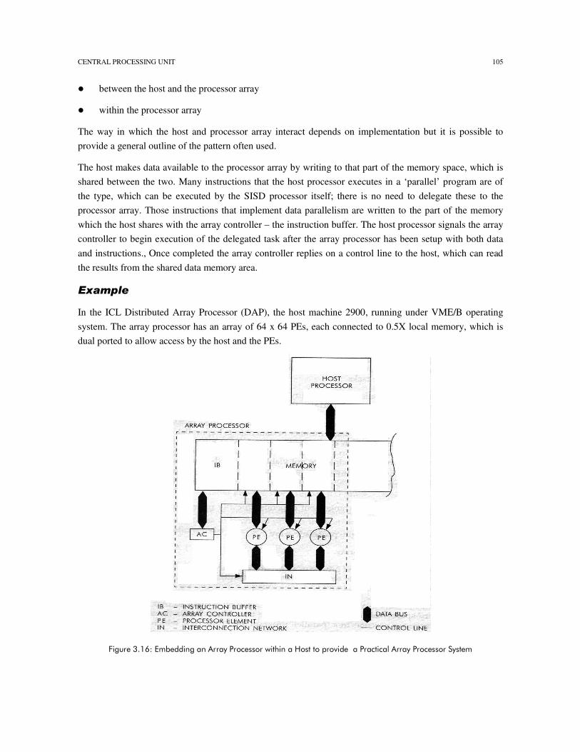
CENTRAL PROCESSING UNIT 105
� between the host and the processor array
� within the processor array
The way in which the host and processor array interact depends on implementation but it is possible to provide a general outline of the pattern often used.
The host makes data available to the processor array by writing to that part of the memory space, which is shared between the two. Many instructions that the host processor executes in a ‘parallel’ program are of the type, which can be executed by the SISD processor itself; there is no need to delegate these to the processor array. Those instructions that implement data parallelism are written to the part of the memory which the host shares with the array controller – the instruction buffer. The host processor signals the array controller to begin execution of the delegated task after the array processor has been setup with both data and instructions., Once completed the array controller replies on a control line to the host, which can read the results from the shared data memory area.
�������
In the ICL Distributed Array Processor (DAP), the host machine 2900, running under VME/B operating system. The array processor has an array of 64 x 64 PEs, each connected to 0.5X local memory, which is dual ported to allow access by the host and the PEs.
�
��������.��"� �$$���� ����� )����#������������� �7����������8�$��� ��� #��# !���� )����#������%)���� ��
COMPUTER SYSTEM ARCHITECTURE 106
The host processor of the Boroughs Scientific Processor (BSP) is the Boroughs B7821. The array processor consists of 16 PEs with a shared-memory of up to 64KB. The interconnection network is a full 16 x 17 crossbar switch. The scalar processor is within the BSP rather that the host, as in the DAP.
Within the processor array, the control strategy again depends on the detailed implementation, particularly:
� sophistication and number of the PEs
� flexibility of the interconnection network
The operation of all processor arrays are based on some common principles: a central controller fetches each instruction from the instruction buffer and broadcasts control signals to all PEs simultaneously. The PEs interpret these signals to operate on local data synchronously. Each PE has access to local memory from which it obtains the data to operate on and to which it returns the result when it has completed the operation. This provision of memory for each PE is a significant difference between the systolic array and this type of processor array. However, there is a fundamental similarity in terms of the method used to synchronize PE operation and the relationship between the PEs and the array controller.
The controller and the PEs share the processing control, each making a contribution within a framework of two control mechanisms:
� Global control: This is a two-way process, with the array controller not only sending out control information (broadcasting instructions), but also receiving status information from each PE. Such information is the equivalent of the flag register in a simple processor system and is necessary for the implementation of conditional branches within the ‘main’ program. There are a number of ways in which the controller can acquire this information but both require the PE to maintain what is effectively a status flag. These are either read selectively by the controller, or they are all attached via a hardwired AND/OR to a control line connected directly to the controller.
� Local control: Each PE receives the broadcasted instruction and decides whether to execute it or not. Again, each PE must make use of a status flag to make this decision. In more complex systems, each PE may be given more than this simple binary control over its own operations, by providing it with a microprogrammable controller. Then, although the same instruction is received by every PE, it is interpreted differently, depending upon the micro-code resident in the local control unit. To implement this flexibility, the array controller must download the appropriate micro code to each PE at the beginning of a run. There are also synchronization problems. Since each micro-operation sequence may be of a different length, the system must have a more sophisticated method of telling when each PE has completed the execution.
Student Activity 3.7
Answer the following questions.
1. Draw a space-time diagram for a six-segment pipeline showing the time it takes to process eight tasks.
2. Determine the number of clock cycles that it takes to process 20 tasks in a six-segment pipeline.
��� � ,�
� Data manipulation instructions perform operations on data and provide the computational capabilities for the computer.
�� A stack is storage device that stores information in such a manner that the item stored last is the first item retrieved LIFO.
�� Program interrupt is used to handle a variety of problems that arise out of normal program sequence.

CENTRAL PROCESSING UNIT 107
�� A parallel processing system is able to perform concurrent data processing to achieve faster execution time.
�� A pipeline can be visualized as a collection of processing segments through which binary information flows.
�� In engineering applications the problems can be formulated in terms of vectors and matrices that tend themselves to vector processing.
�
�
���(������� ����.����� ���
� �� ����%�����&��'��(
1. SIMD stands for ___________ instruction stream, multiple data stream.
2. ____________ control is faster than microprogrammed control.
���)���
1. single
2. Hardwired
!���������&��'��(
1. Indexing is one of the addressing mode.
2. MOV X is used to upload instruction in the processor.
���)���
1. True
2. False
� �� ����%�����&*���'��(
1. In stack the values are stored in ________ form.
2. __________ is a visualisation of processing segments collection.
!���������&*���'��(
1. Stack organized processor does not use address field for instructor ADD or MUL.
2. PSW stands for program stack word.
'�������.����� ���
1. A relative mode branch type of instruction is stored in memory at an address equivalent to decimal 750. The branch is made to an address equivalent to decimal 500.

COMPUTER SYSTEM ARCHITECTURE 108
(a) What should be the value of the relative address field of the instruction in decimal?
(b) Determine the relative address value in binary using 12 bits.
2. Write a program to evaluate the arithmetic statement
(a) Using a general purpose register with three address instructions.
(b) Using an accumulator type computer with one address instruction.
3. Perform the logic AND, OR , and XOR with the two binary strings 11011101 and 11001111.