Embed Size (px)
Citation preview
Chapter 1 Microcomputers and Microprocessors
Microprocessor Evolution and Performance
Contents
Introduction to microcomputer systemMicroprocessor evolution
the INTEL processor family
Microprocessor performance
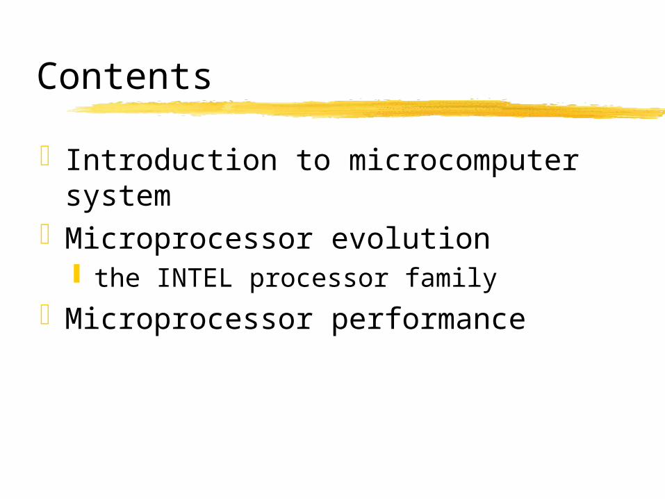
Introduction to Microcomputer
An microcomputer can be interpreted as a machine with: I/O devices for Input/Output, microprocessor for processing, memory units for storage Buses for connecting the above components
In 1970, a microcomputer was normally interpreted as a computer considerably smaller than a mini-computer, possibly using ROM for program storage
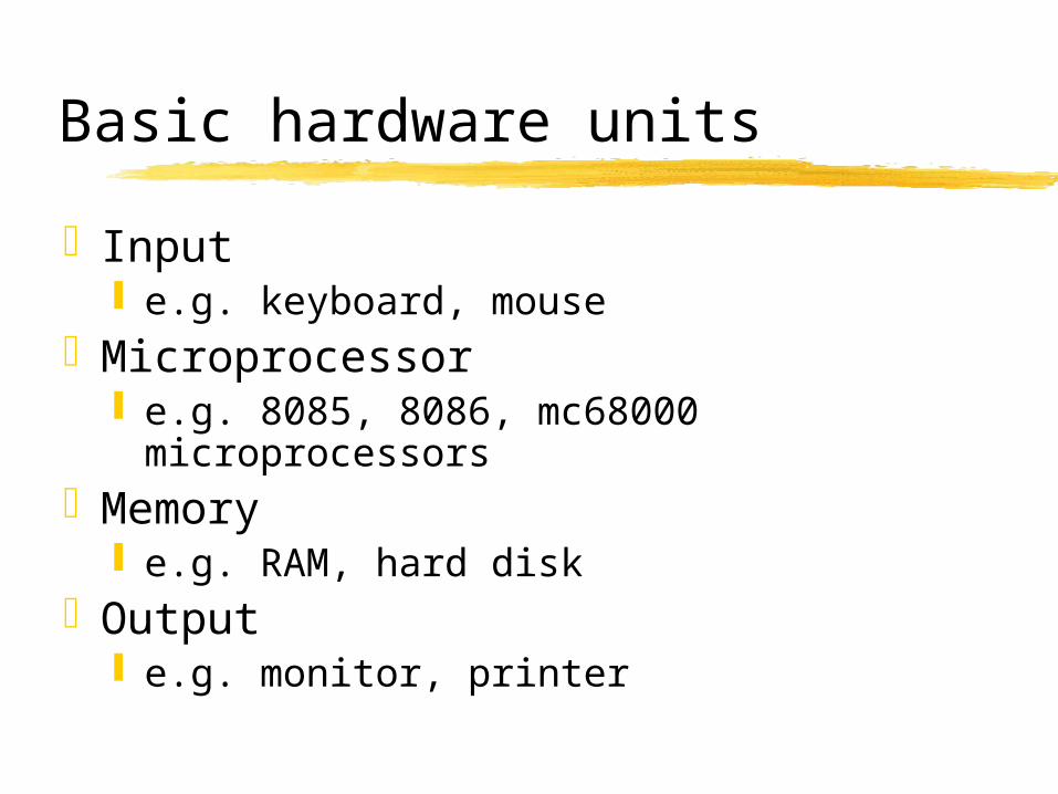
Basic hardware units
Input e.g. keyboard, mouse
Microprocessor e.g. 8085, 8086, mc68000 microprocessors
Memory e.g. RAM, hard disk
Output e.g. monitor, printer
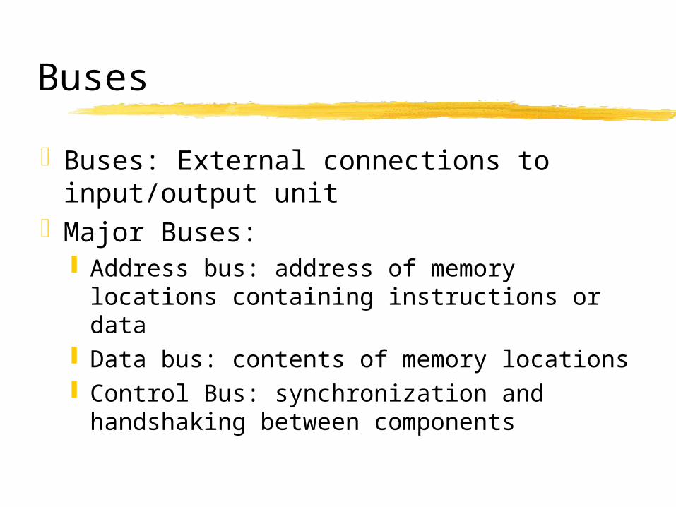
Buses
Buses: External connections to input/output unit
Major Buses: Address bus: address of memory locations
containing instructions or data Data bus: contents of memory locations Control Bus: synchronization and handshaking
between components
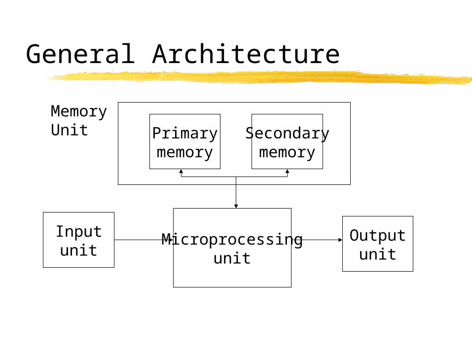
General Architecture
Inputunit
Microprocessingunit
Outputunit
Secondarymemory
Primarymemory
MemoryUnit
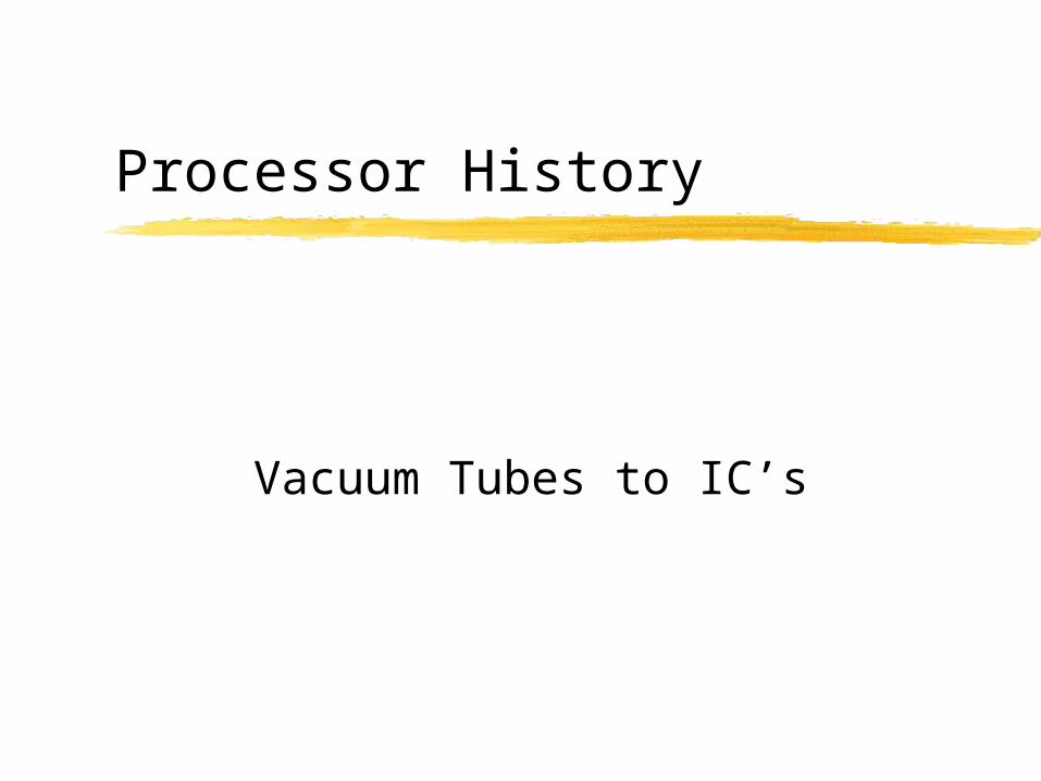
Processor History
Vacuum Tubes to IC’s
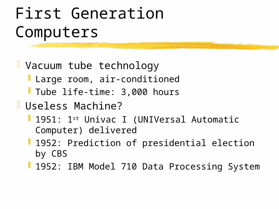
First Generation Computers
Vacuum tube technology Large room, air-conditioned Tube life-time: 3,000 hours
Useless Machine? 1951: 1st Univac I (UNIVersal Automatic
Computer) delivered 1952: Prediction of presidential election by CBS 1952: IBM Model 710 Data Processing System
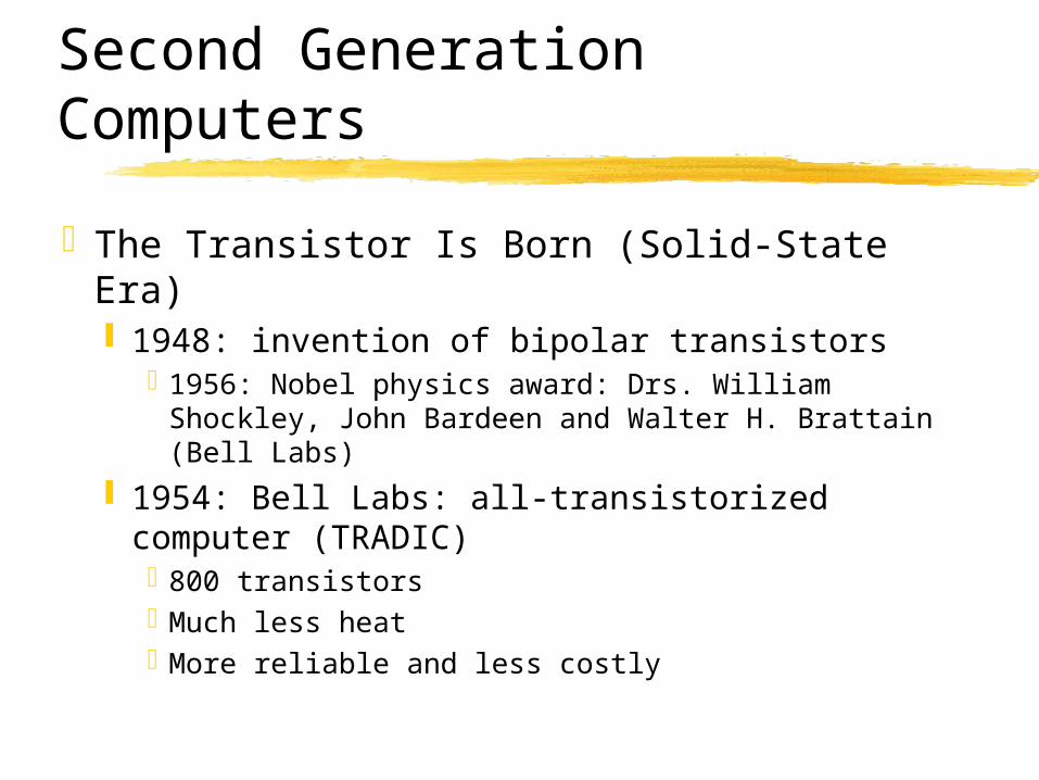
Second Generation Computers
The Transistor Is Born (Solid-State Era) 1948: invention of bipolar transistors
1956: Nobel physics award: Drs. William Shockley, John Bardeen and Walter H. Brattain (Bell Labs)
1954: Bell Labs: all-transistorized computer (TRADIC)800 transistorsMuch less heatMore reliable and less costly
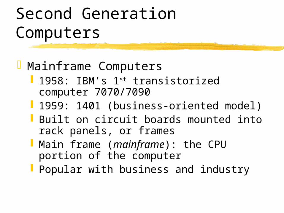
Second Generation Computers
Mainframe Computers 1958: IBM’s 1st transistorized computer
7070/7090 1959: 1401 (business-oriented model) Built on circuit boards mounted into rack panels,
or frames Main frame (mainframe): the CPU portion of the
computer Popular with business and industry
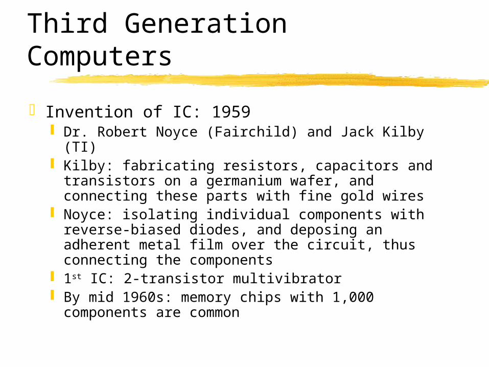
Third Generation Computers
Invention of IC: 1959 Dr. Robert Noyce (Fairchild) and Jack Kilby (TI) Kilby: fabricating resistors, capacitors and transistors on a
germanium wafer, and connecting these parts with fine gold wires
Noyce: isolating individual components with reverse-biased diodes, and deposing an adherent metal film over the circuit, thus connecting the components
1st IC: 2-transistor multivibrator By mid 1960s: memory chips with 1,000 components are
common
Third Generation Computers
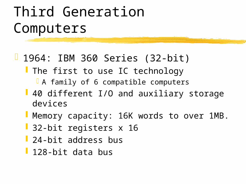
1964: IBM 360 Series (32-bit) The first to use IC technology
A family of 6 compatible computers
40 different I/O and auxiliary storage devices Memory capacity: 16K words to over 1MB. 32-bit registers x 16 24-bit address bus 128-bit data bus
Third Generation Computers
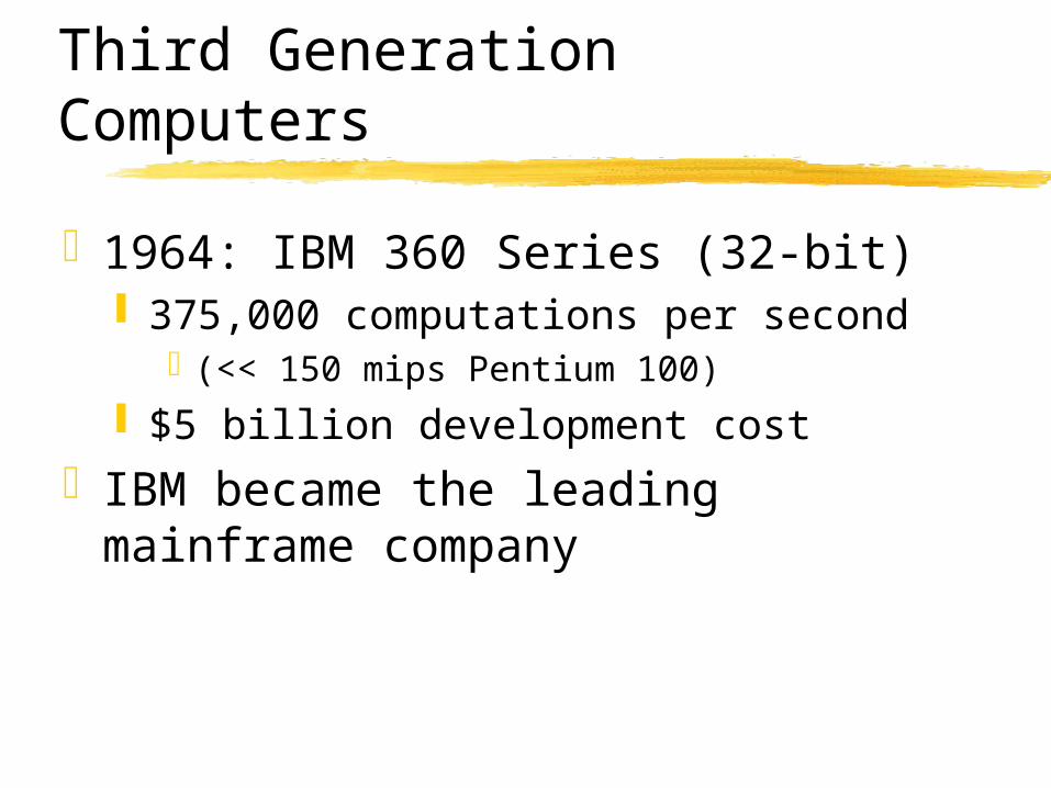
1964: IBM 360 Series (32-bit) 375,000 computations per second
(<< 150 mips Pentium 100)
$5 billion development cost
IBM became the leading mainframe company
Minicomputer
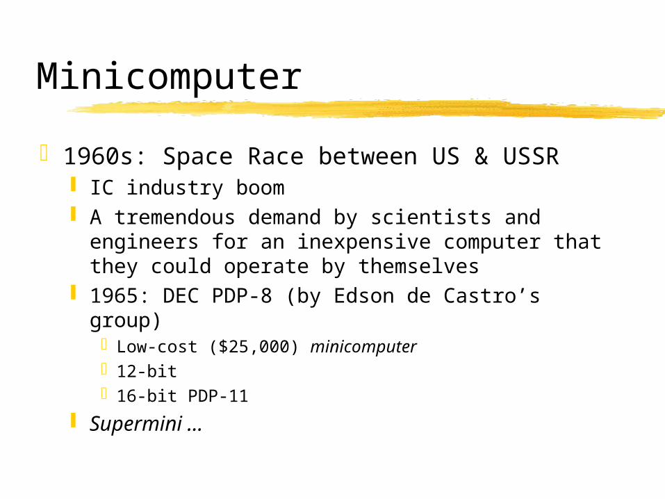
1960s: Space Race between US & USSR IC industry boom A tremendous demand by scientists and engineers for an
inexpensive computer that they could operate by themselves
1965: DEC PDP-8 (by Edson de Castro’s group)Low-cost ($25,000) minicomputer12-bit16-bit PDP-11
Supermini …
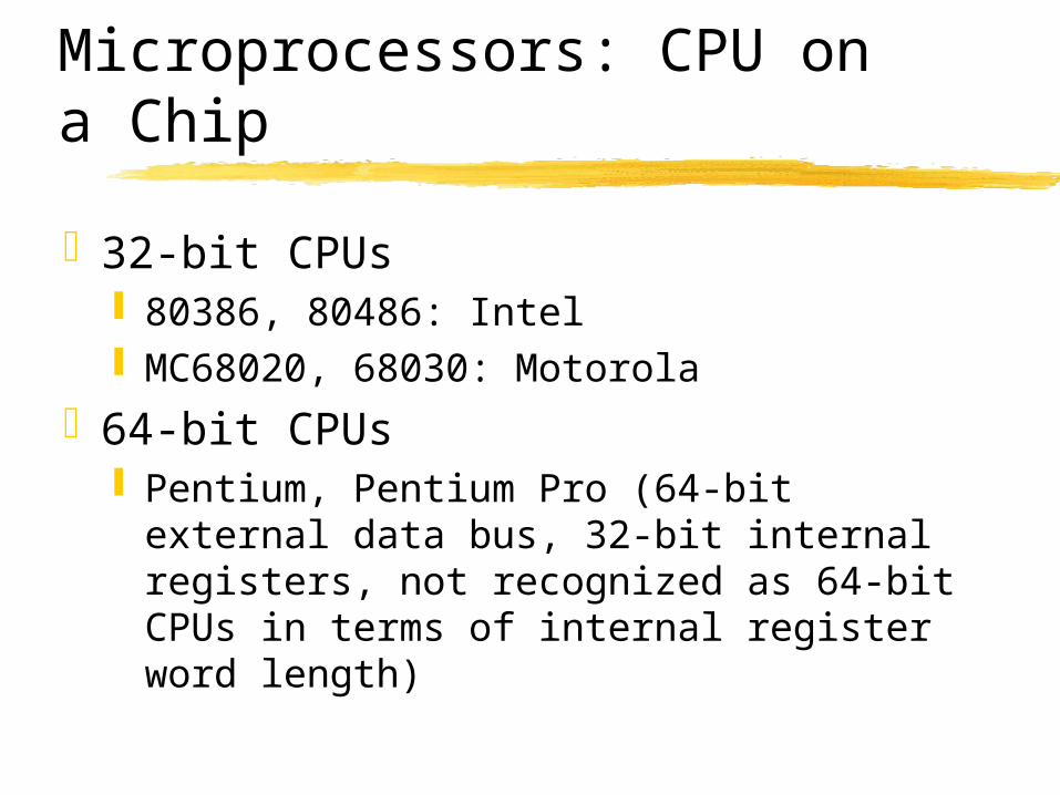
Microprocessors: CPU on a Chip
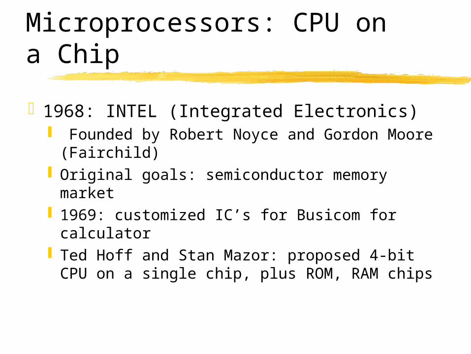
1968: INTEL (Integrated Electronics) Founded by Robert Noyce and Gordon Moore
(Fairchild) Original goals: semiconductor memory market 1969: customized IC’s for Busicom for calculator Ted Hoff and Stan Mazor: proposed 4-bit CPU on
a single chip, plus ROM, RAM chips
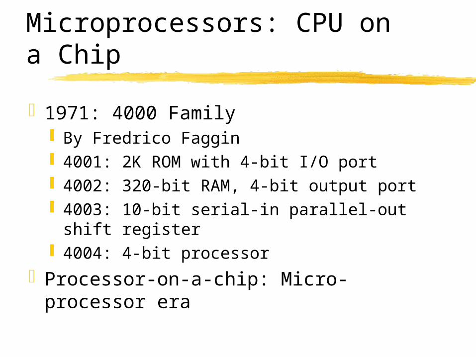
Microprocessors: CPU on a Chip
1971: 4000 Family By Fredrico Faggin 4001: 2K ROM with 4-bit I/O port 4002: 320-bit RAM, 4-bit output port 4003: 10-bit serial-in parallel-out shift register 4004: 4-bit processor
Processor-on-a-chip: Micro-processor era
Microprocessors: CPU on a Chip
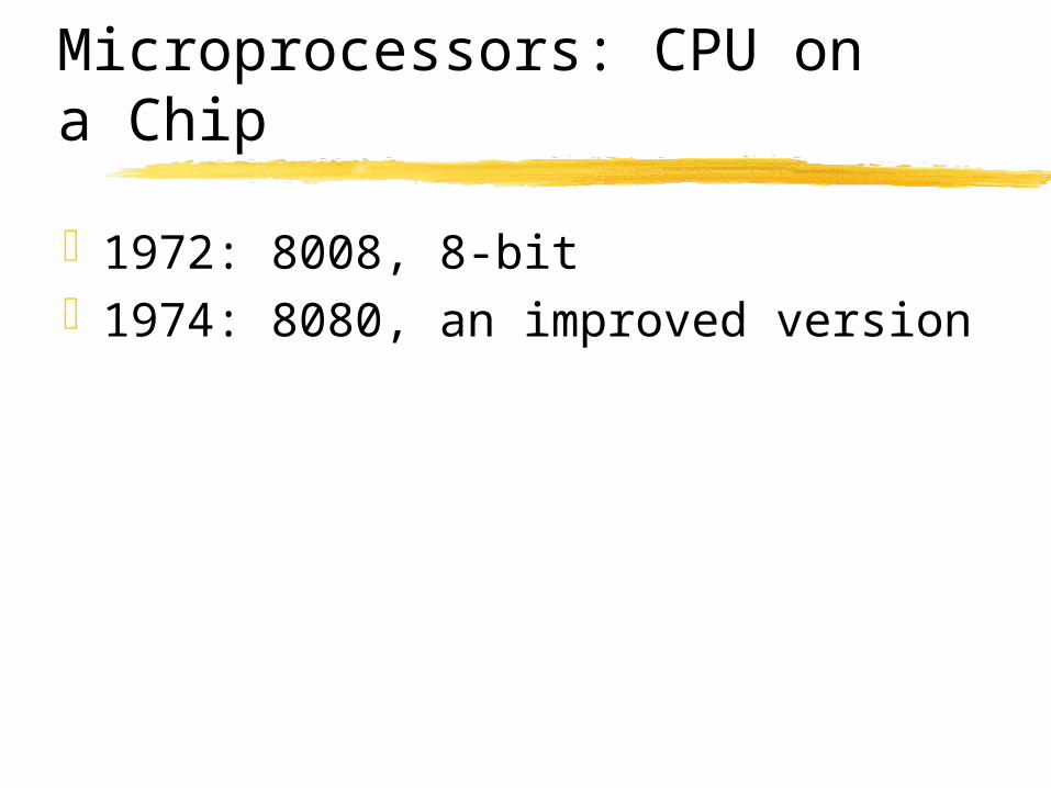
1972: 8008, 8-bit1974: 8080, an improved version
Microprocessors: CPU on a Chip
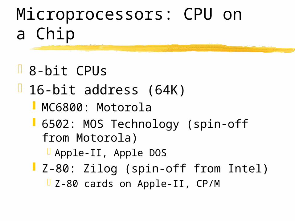
8-bit CPUs16-bit address (64K)
MC6800: Motorola 6502: MOS Technology (spin-off from Motorola)
Apple-II, Apple DOS
Z-80: Zilog (spin-off from Intel)Z-80 cards on Apple-II, CP/M
Microprocessors: CPU on a Chip
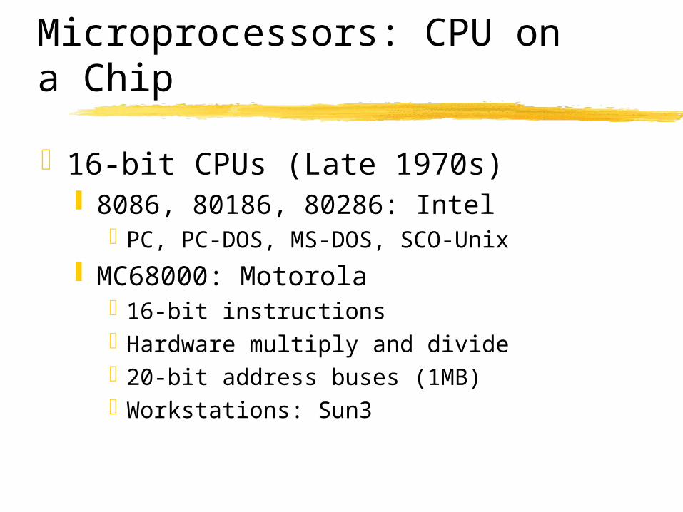
16-bit CPUs (Late 1970s) 8086, 80186, 80286: Intel
PC, PC-DOS, MS-DOS, SCO-Unix
MC68000: Motorola16-bit instructionsHardware multiply and divide20-bit address buses (1MB)Workstations: Sun3
Microprocessors: CPU on a Chip
32-bit CPUs 80386, 80486: Intel MC68020, 68030: Motorola
64-bit CPUs Pentium, Pentium Pro (64-bit external data bus,
32-bit internal registers, not recognized as 64-bit CPUs in terms of internal register word length)
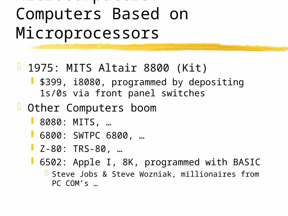
Microcomputers: Computers Based on Microprocessors
1975: MITS Altair 8800 (Kit) $399, i8080, programmed by depositing 1s/0s via front
panel switches
Other Computers boom 8080: MITS, … 6800: SWTPC 6800, … Z-80: TRS-80, … 6502: Apple I, 8K, programmed with BASIC
Steve Jobs & Steve Wozniak, millionaires from PC COM’s …
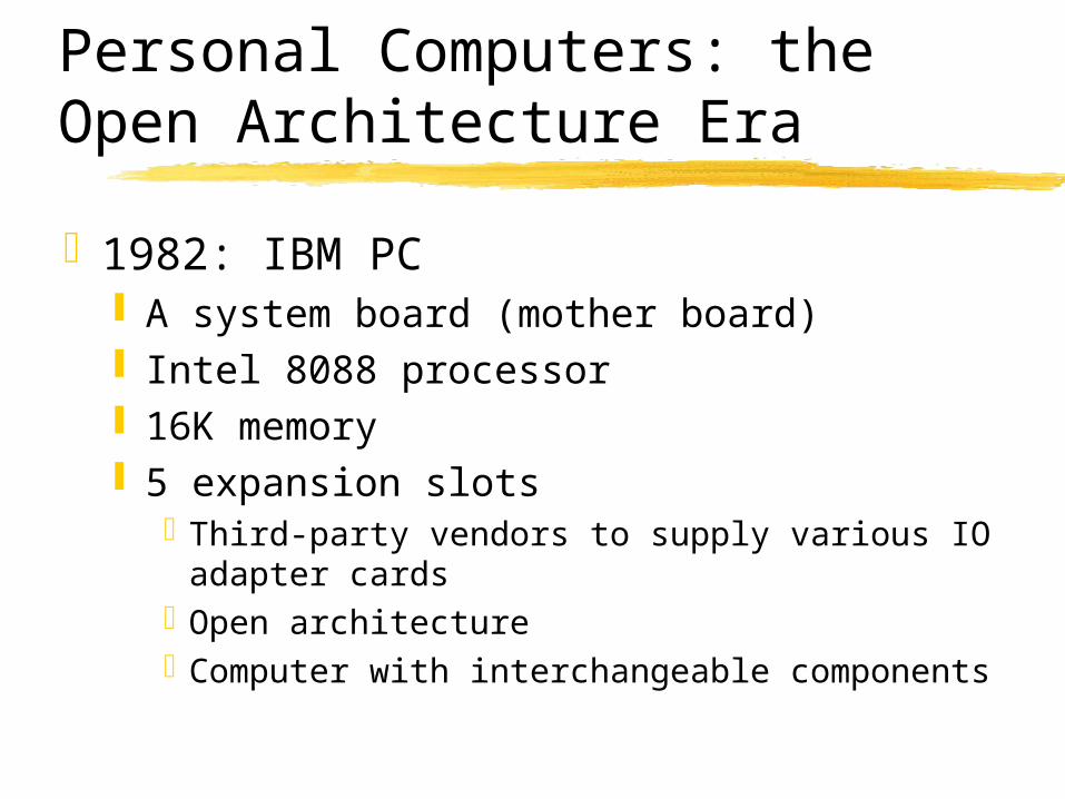
Personal Computers: the Open Architecture Era
1982: IBM PC A system board (mother board) Intel 8088 processor 16K memory 5 expansion slots
Third-party vendors to supply various IO adapter cardsOpen architectureComputer with interchangeable components
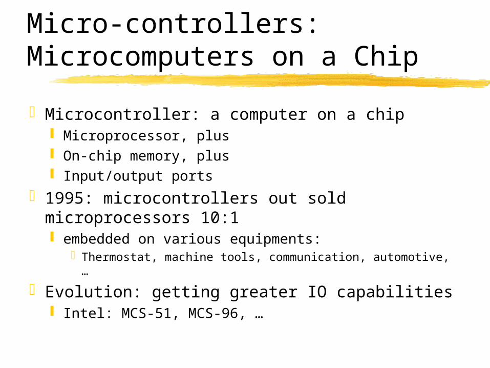
Micro-controllers: Microcomputers on a Chip
Microcontroller: a computer on a chip Microprocessor, plus On-chip memory, plus Input/output ports
1995: microcontrollers out sold microprocessors 10:1 embedded on various equipments:
Thermostat, machine tools, communication, automotive, …
Evolution: getting greater IO capabilities Intel: MCS-51, MCS-96, …
High-Performance Processors
Supercomputers Aircraft design, global climate modeling, oil-
bearing formation, molecular design of new drugs, financial behavior
CDC6600, 7600: Seymour Cray Cray-1: 1976, the first true supercomputer
ECL, 128 KW power consumption130 MFLOPS (Pentium 100: 150 MFLOPS)$5.1 million
High-Performance Processors
Parallel Processors Tens of gigaflops Multi-processors wired by a common bus Each is given a portion of the problem to solve Hypercube: early 1980s
Cosmic Cube, iPSC (with i860/RISC chips)
2D rectangular Mesh architecture: multiple processor at each node
Intel: teraflops computer with 4500 nodes, each powered by 2 Pentium Pro 200.
RISC vs. CISC
RISC: Reduced Instruction Set Computer (1980s) A small number of fixed-length instructions Simple addressing modes A large number of registers Instructions executed in one clock cycle
Intel i860 (“Cray on a Chip”) 82 instructions, 32-bit long each Four addressing modes 32 general-purpose registers
RISC vs. CISC
CISC: Complex Instruction Set Computer A large number of variable length instructions Multiple addressing modes A small number of registers Multiple number of clock cycles to execute
Intel 8086 Over 3000 instruction forms, 1-6 bytes 9 addressing modes 8 general-purpose registers Execution from 2 to 80+ cycles
RISC vs. CISC
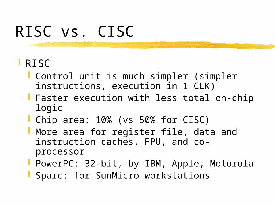
RISC Control unit is much simpler (simpler instructions,
execution in 1 CLK) Faster execution with less total on-chip logic Chip area: 10% (vs 50% for CISC) More area for register file, data and instruction
caches, FPU, and co-processor PowerPC: 32-bit, by IBM, Apple, Motorola Sparc: for SunMicro workstations
Application-Specific Processors
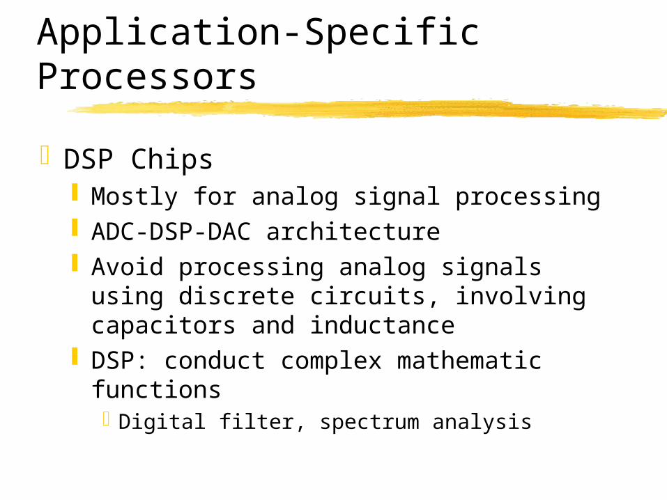
DSP Chips Mostly for analog signal processing ADC-DSP-DAC architecture Avoid processing analog signals using discrete
circuits, involving capacitors and inductance DSP: conduct complex mathematic functions
Digital filter, spectrum analysis
Application-Specific Processors
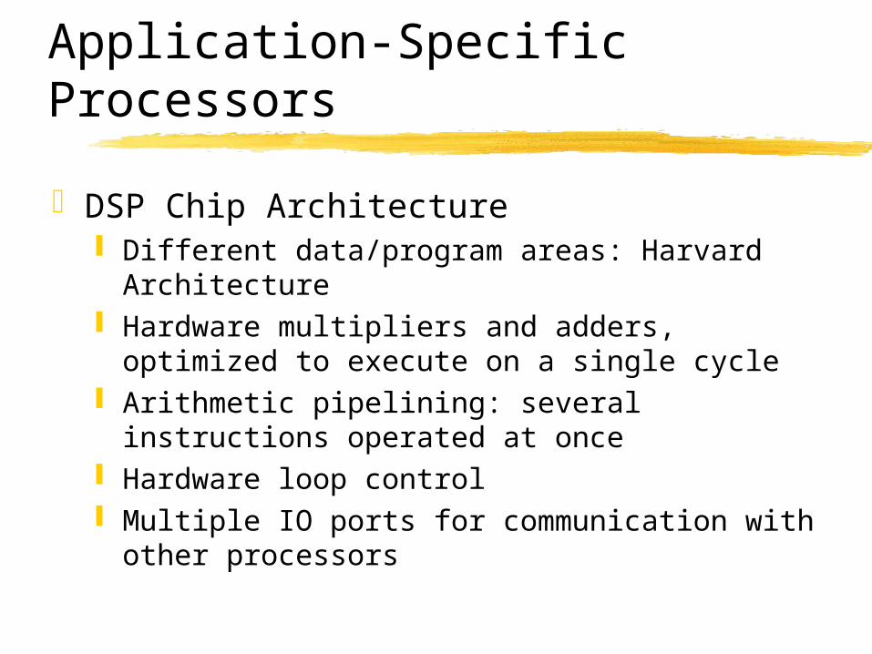
DSP Chip Architecture Different data/program areas: Harvard Architecture Hardware multipliers and adders, optimized to execute on
a single cycle Arithmetic pipelining: several instructions operated at once Hardware loop control Multiple IO ports for communication with other processors
Summary of Processor History
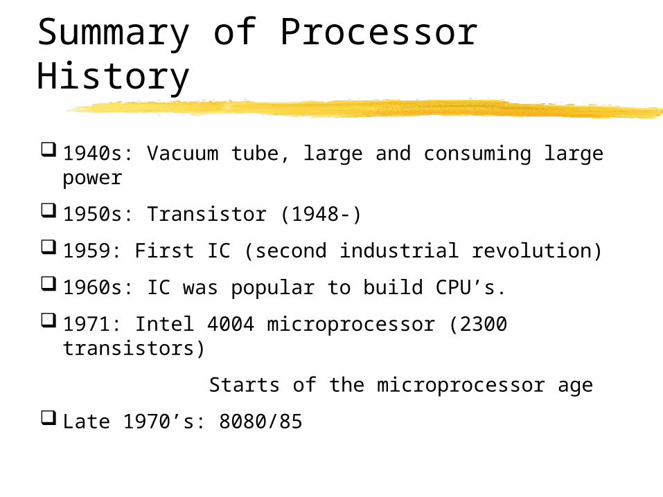
1940s: Vacuum tube, large and consuming large power
1950s: Transistor (1948-)
1959: First IC (second industrial revolution)
1960s: IC was popular to build CPU’s.
1971: Intel 4004 microprocessor (2300 transistors)
Starts of the microprocessor age
Late 1970’s: 8080/85
Summary of Processor History
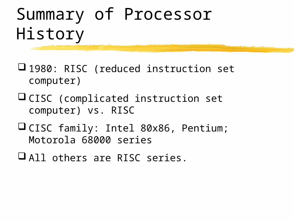
1980: RISC (reduced instruction set computer)
CISC (complicated instruction set computer) vs. RISC
CISC family: Intel 80x86, Pentium; Motorola 68000 series
All others are RISC series.
Evolution of INTEL Processors
4004 (’71)-Pentium Pro (’93-)
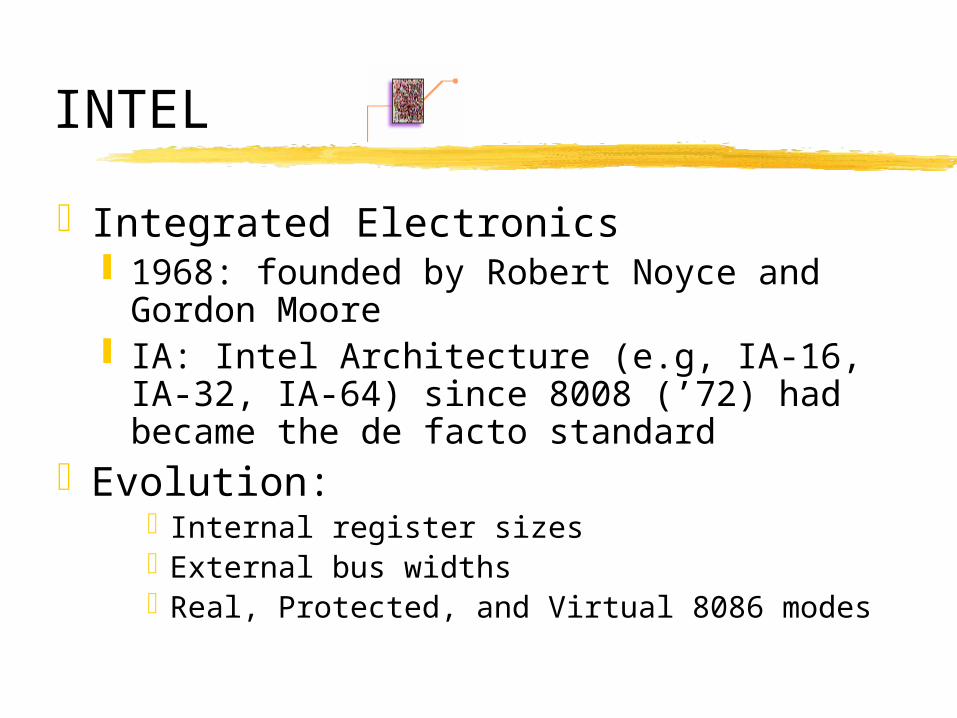
INTEL
Integrated Electronics 1968: founded by Robert Noyce and Gordon
Moore IA: Intel Architecture (e.g, IA-16, IA-32, IA-64)
since 8008 (’72) had became the de facto standardEvolution:
Internal register sizesExternal bus widthsReal, Protected, and Virtual 8086 modes
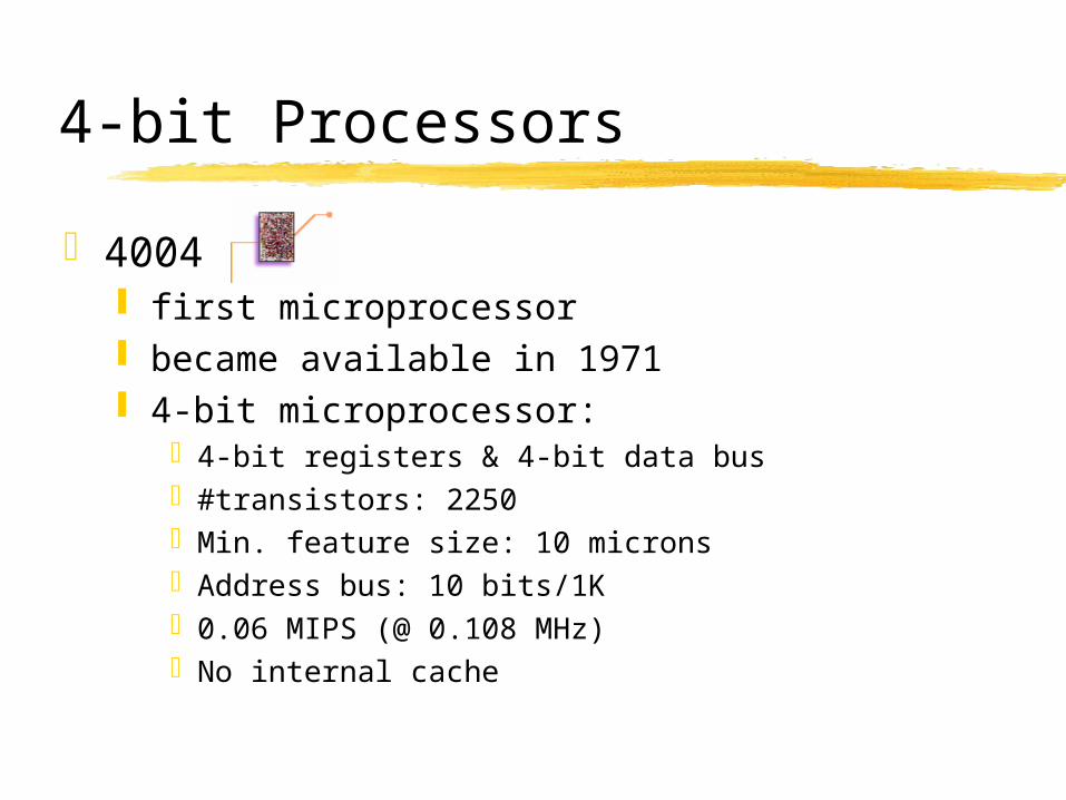
4-bit Processors
4004 first microprocessor became available in 1971 4-bit microprocessor:
4-bit registers & 4-bit data bus#transistors: 2250Min. feature size: 10 micronsAddress bus: 10 bits/1K0.06 MIPS (@ 0.108 MHz)No internal cache
8-bit Processors
8008, 8080, 8085 became available in 1974 8-bit microprocessor
8080

8086: IA standard
Became available in 1978 16-bit data bus 20-bit address bus (was 16-bit for 8080) memory organization: 16 segments of 64KB (1 MB limit)
Re-organize CPU into BIU (bus interface unit) and EU (execution unit) Allow fetch and execution simultaneously
Internal register expanded to 16-bit Allow access of low/high byte separately
8086
Hardware multiply and divide instructionsExternal math co-processorInstruction set compatible with 8080/80858086: defined the 80x86 architecture
8086
Not quite successful 16-bit data bus: Requires two separate 8-bit memory
banks Memory chips were expensive
8088: PC standard
Became available in 1979, almost identical to 80868-bit data bus: for hardware compatibility with 808016-bit internal registers and data bus (same as 8086)20-bit address bus (was 16-bit for 8080)
BIU re-designedmemory organization: 16 segments of 64KB (1 MB limit)
Two memory accesses for 16-bit data (less efficient) But less cost
8088: used by IBM PC (1982), 16K-64K, 4.77MHz
80186, 80188: High Integration CPU
PC system: 8088 CPU + various supporting chips
Clock generator8251: serial IO (RS232)8253: timer/counter8255: PPI (programmable periphial interface)8257: DMA controller8259: interrupt controller
80186/80188: 8086/8088 + supporting functions Compatible instruction set (+ 9 new instructions)
80286
Became available in 1982used in IBM AT computer (1984)16-bit data busclock speed 25% faster than 8088, throughput
5 times greater than 808824-bit address bus (16 MB) (vs. 20-bit/1M
8086)

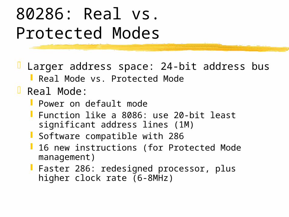
80286: Real vs. Protected Modes
Larger address space: 24-bit address bus Real Mode vs. Protected Mode
Real Mode: Power on default mode Function like a 8086: use 20-bit least significant address
lines (1M) Software compatible with 286 16 new instructions (for Protected Mode management) Faster 286: redesigned processor, plus higher clock rate (6-
8MHz)

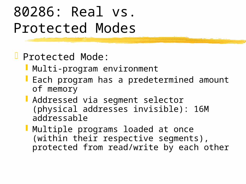
80286: Real vs. Protected Modes
Protected Mode: Multi-program environment Each program has a predetermined amount of
memory Addressed via segment selector (physical
addresses invisible): 16M addressable Multiple programs loaded at once (within their
respective segments), protected from read/write by each other
80286: Real vs. Protected Modes
Protected Mode: Cannot be switch back to real mode to avoid
illegal access by switching back and forth between modes
A faster 8086 only? MS-DOS requires that all programs be run in Real
Mode
Clock Speed
Electrical signals cannot change instantaneously (transition period required)
System clock provides timing signal for synchronization
Cannot be used to compare the performance of microprocessors with different instruction sets e.g., a 66 MHz Pentium is twice as fast as a 66 MHz
80486

80386DX (aka. 80386)
available in 1985, a major redesign of 86/286 Compatibility commitment through 2000
32-bit data and address buses (4 GB memory) Real Address Mode: 1M visible, 286 real mode Protected Virtual Address Mode:
On board MMUSegmented tasks of 1byte to 4G bytes
• Segment base, limit, attributes defined by a descriptor register
Page swapping: 4K pages, up to 64TB virtual memory spaceWindows, OS/2, Unix/Linux

80386DX (aka. 80386)
Virtual 8086 mode (a special Protected mode feature): permitted multiple 8086 virtual machines-multitasking (similar to real mode) Windows (multiple MSDOS’s)
Clock rate: max. 40MHz, 2 pulses per R/W bus cycle External memory cache to avoid wait
Fast SRAM93% hit rate with 64K cache
Compatible instructions (14 new)
80386SX
80386SX: (for transition to 32-bit) 16-bit data bus/32-bit register 24-bit address bus
80486DX
1989: a polished 386, 6 new OS level instructionsvirtually identical to 386 in terms of compatibilityRISC design concepts
fewer clock cycles per operation, a single clock cycle for most frequently used instructions
Max 50MHz 5 stage execution pipeline
Portions of 5 instructions execute at once
80486DX
Highly Integrated: On board 8K memory cache FPP (equivalent to external 80387 co-processor)
Twice as fast as 386 at any given clock rate 20Mhz 486 ~= 40Mhz 386

80486SX
80486SX NOT a 16-bit version for transition purpose no coprocessor No internal cache For low-end applications Max. 33Mhz only

80486DX2/DX4: Overdrive Chips
Processor speed increased too fast Redesign of microcomputer for compatibility
becomes harder Solution: Separating internal speed with external
speed, improve performance independently
80486DX2/DX4 – internal clock twice/three times (NOT four times) the external clock: runs faster internally

80486DX2/DX4: Overdrive Chips
System board design is independent of processor upgrade (less expensive components are allowed)
Processor operate at maximum speed data rate internally Only slow access to external data operates at system board rate Internal cache offset the speed gap
486DX2 66: 66 internal, 33 external486DX4 100: 100 internal, 33 external (3x)Overdrive sockets: for upgrading 486dx/sx to
486dx2/dx4 (with overdrive socket pin-outs)

Pentium: Superscaler Processor
available in 199232-bit architectureSuperscaler architecture
Scaling: scaling down etchable feature size to increase complexity of IC (e.g., DRAM)
10 microns/4004 to 0.13 microns (2001) Superscaler: go beyond simply scaling down Two instruction pipelines: each with own ALU, address
generation circuitry, data cache interface Execute two different instructions simultaneously
Pentium: Superscaler Processor
Onboard cache Separate 8K data and code caches to avoid access
conflictsFPPInstruction pipeline: 8 stageOptimized floating point functions
5x-10x FLOP’s of 486 2x performance of 486 at any clock rate
Pentium: Superscaler Processor
Compatibility with 386/486: Internal 32-bit registers and address bus Data bus expanded to 64-bits for higher data
transfer rateCompare 8088 to 386sx transition
Pentium: Superscaler Processor
non-clone competition from AMD, Cyrixdevelopment of brand identity by Intel
Pentium Pro: Two Chips in One
Became available in 1995Superscaler of degree 3
Can execute 3 instructions simultaneously
Optimized for 32-bit operating systems (e.g., Windows NT, OS2/Warp)
Two separate silicon die on the same package Processor: 0.35 u, 5.5 million transistors 256KB(/512K) Level 2 cache included on chip, 15.5
million transistors in smaller area
Pentium Pro: Two Chips in One
On Board Level 2 cache Simplifies system board design Requires less space Gains faster communication with processor
Internal (level 1) cache: 8KPentium Pro 133 ~= 2x Pentium 66 ~= 4x
486DX2 66

Pentium Pro:Dynamic Execution
Dynamic execution: reduce idle processor time by predicting instruction behaviors Multiple Branch Prediction: look as far as 30 instructions
ahead to anticipate program branches Data Flow Analysis: looks at upcoming instructions and
determine if they are available for processing, depending on other instructions. Determine optimal execution sequences.
Speculative Execution: execute instructions in different order as entered. Speculative results are stored until final states can be determined.

Processor Future
What’s More from Moore’s Law?
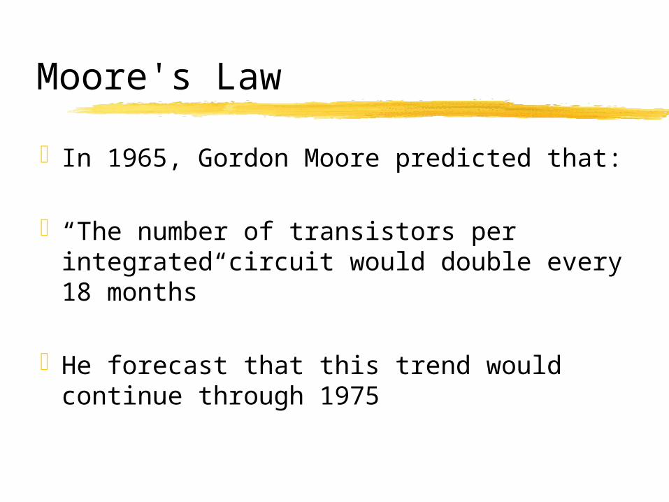
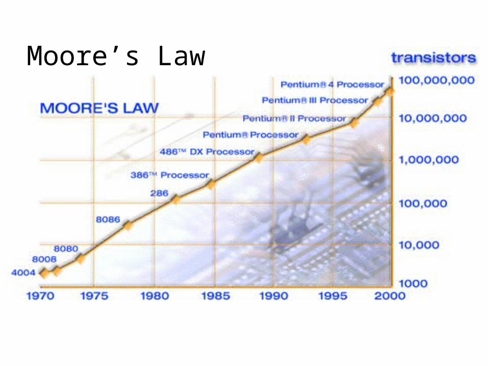
Moore's Law
In 1965, Gordon Moore predicted that:
“The number of transistors per integrated circuit would double every 18 months”
He forecast that this trend would continue through 1975
Moore’s Law
Other Microprocessors
Motorola family from 6809 (Apple II) through 68040
PowerPC joint venture between Apple, IBM, and Motorola
RISC Processors DEC Alpha, MIPS, Sun SPARC, etc.
CISC vs. RISC
CISC (Complex Instruction Set Computer) CISC processors have a large versatile instruction
set that supports many complex addressing modes move complexity from software to hardware
RISC (Reduced Instruction Set Computer) RISC processors have a small instruction set move complexity from hardware to software
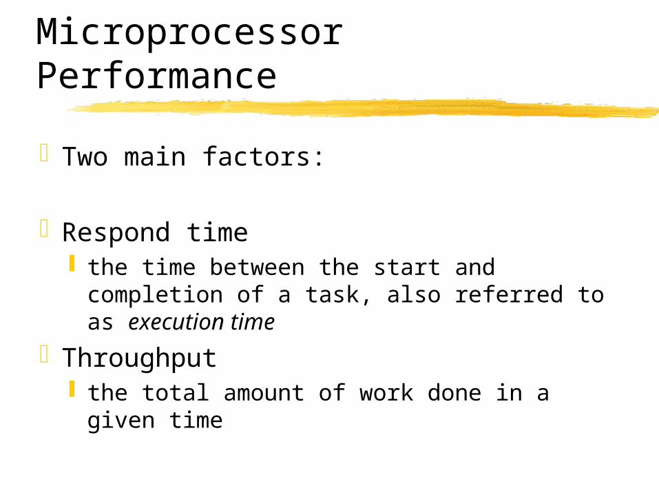
Microprocessor Performance
Two main factors:
Respond time the time between the start and completion of a
task, also referred to as execution time
Throughput the total amount of work done in a given time
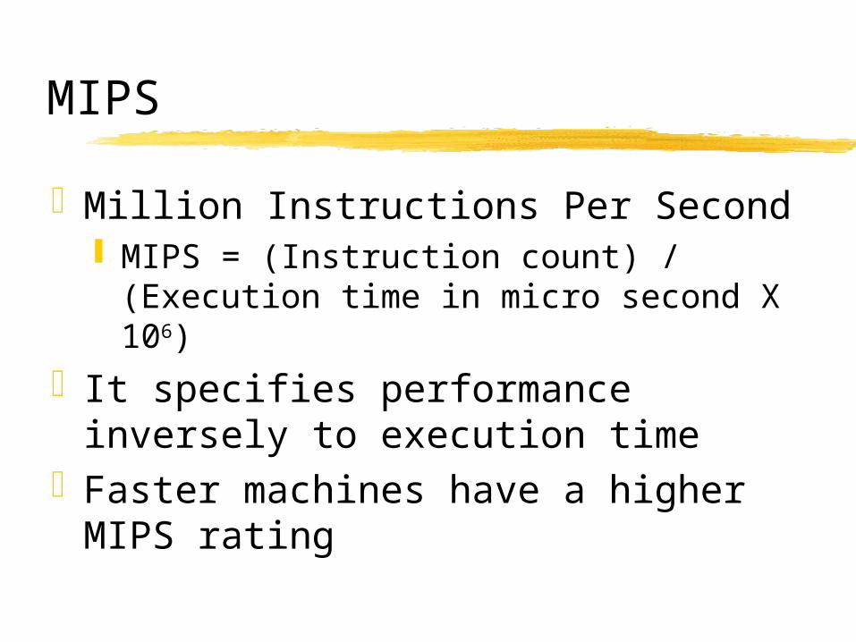
MIPS
Million Instructions Per Second MIPS = (Instruction count) / (Execution time in micro
second X 106)
It specifies performance inversely to execution time
Faster machines have a higher MIPS rating
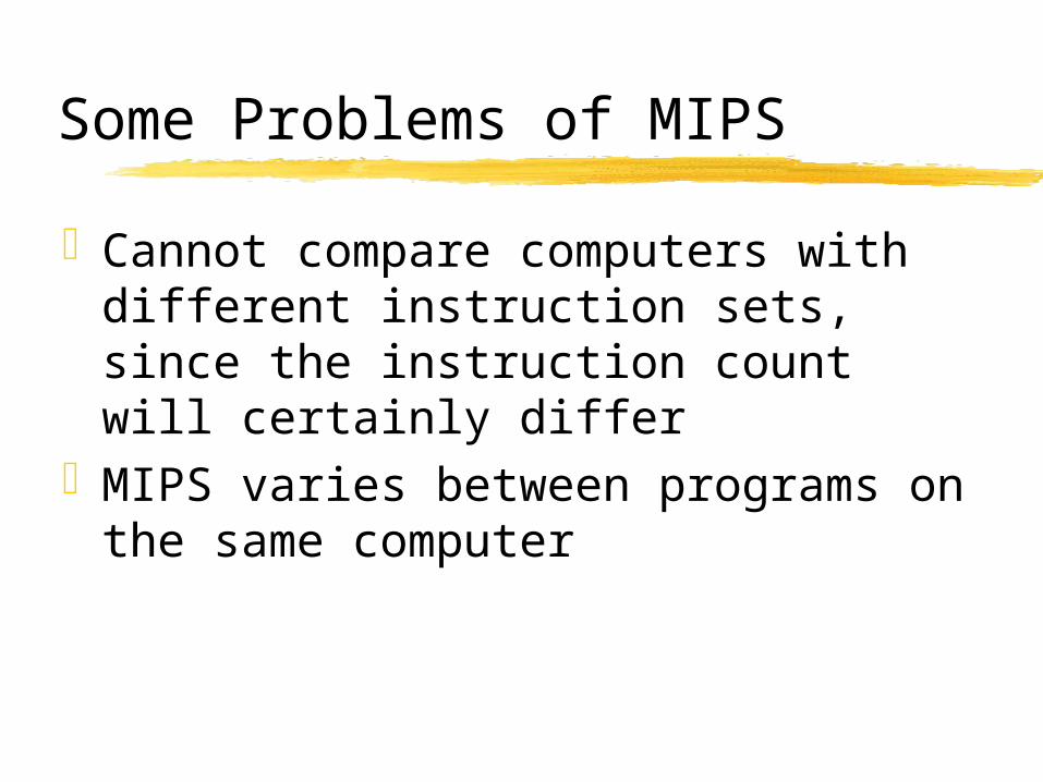
Some Problems of MIPS
Cannot compare computers with different instruction sets, since the instruction count will certainly differ
MIPS varies between programs on the same computer
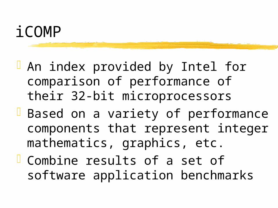
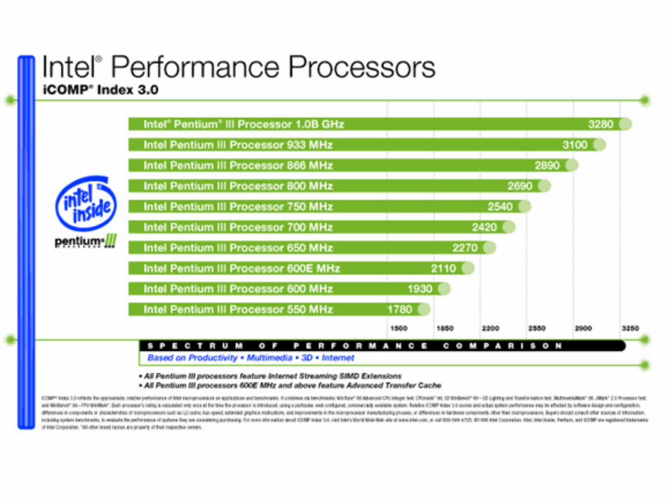
iCOMP
An index provided by Intel for comparison of performance of their 32-bit microprocessors
Based on a variety of performance components that represent integer mathematics, graphics, etc.
Combine results of a set of software application benchmarks
Chapter 2Computer Codes, Programming, and Operating Systems
Number SystemsComputer CodesProgrammingOperating Systems
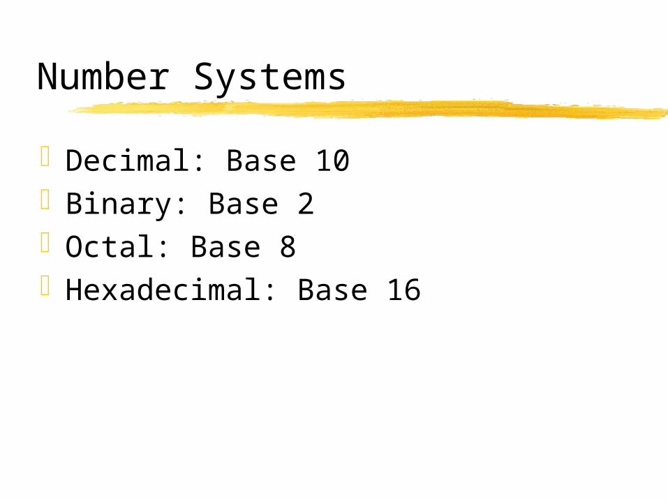
Number Systems
Decimal: Base 10Binary: Base 2Octal: Base 8Hexadecimal: Base 16
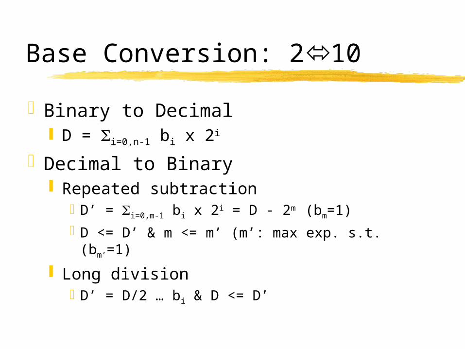
Base Conversion: 210
Binary to Decimal D = i=0,n-1 bi x 2i
Decimal to Binary Repeated subtraction
D’ = i=0,m-1 bi x 2i = D - 2m (bm=1)
D <= D’ & m <= m’ (m’: max exp. s.t. (bm’=1)
Long divisionD’ = D/2 … bi & D <= D’

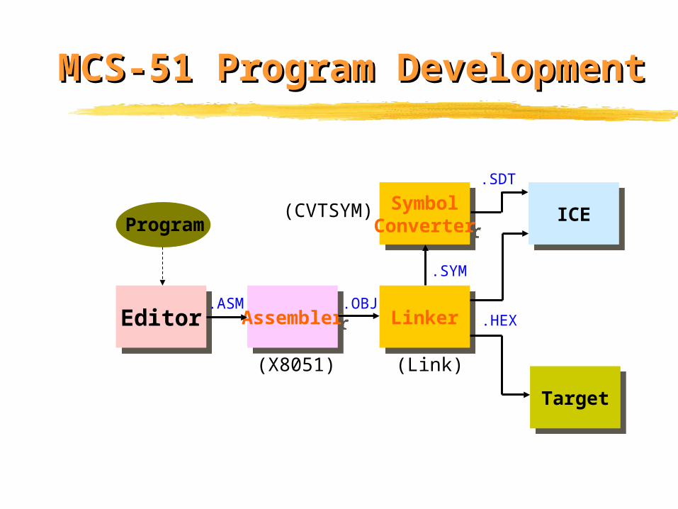
MCS-51 Program DevelopmentMCS-51 Program Development
EditorEditor AssemblerAssembler LinkerLinker
SymbolConverter
SymbolConverter ICEICE
TargetTarget
Program
.ASM .OBJ.HEX
.SYM
.SDT
(X8051) (Link)
(CVTSYM)
Chapter 380x86 Processor Architecture
8086/88Segmented Memory8038680486PentiumPentium Pro
The 8086 and 8088
Processor ModelProgramming Model
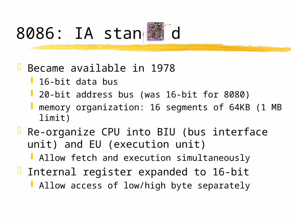
8086: IA standard
Became available in 1978 16-bit data bus 20-bit address bus (was 16-bit for 8080) memory organization: 16 segments of 64KB (1 MB limit)
Re-organize CPU into BIU (bus interface unit) and EU (execution unit) Allow fetch and execution simultaneously
Internal register expanded to 16-bit Allow access of low/high byte separately

8088: PC standard
Became available in 1979, almost identical to 80868-bit data bus: for hardware compatibility with 808016-bit internal registers and data bus (same as 8086)20-bit address bus (was 16-bit for 8080)
BIU re-designedmemory organization: 16 segments of 64KB (1 MB limit)
Two memory accesses for 16-bit data (less efficient) But less cost
8088: used by IBM PC (1982), 16K-64K, 4.77MHz

80186, 80188: High Integration CPU
PC system: 8088 CPU + various supporting chips
Clock generator8251: serial IO (RS232)8253: timer/counter8255: PPI (programmable periphial interface)8257: DMA controller8259: interrupt controller
80186/80188: 8086/8088 + supporting functions Compatible instruction set (+ 9 new instructions)
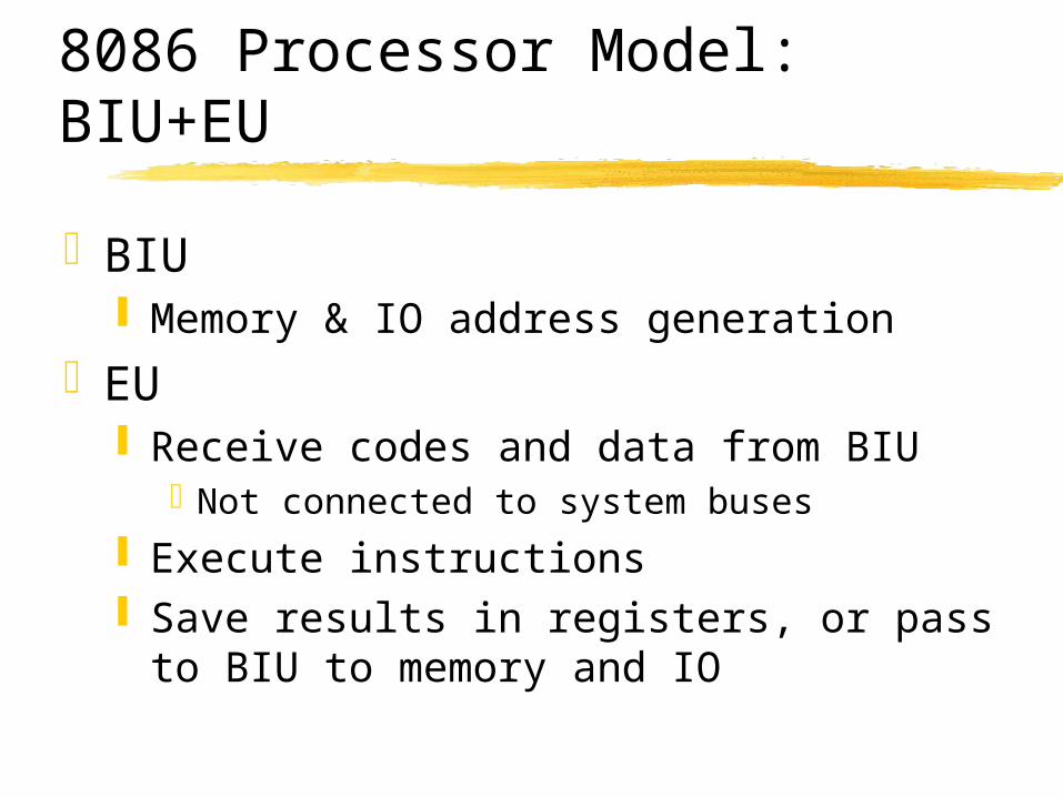
8086 Processor Model: BIU+EU
BIU Memory & IO address generation
EU Receive codes and data from BIU
Not connected to system buses
Execute instructions Save results in registers, or pass to BIU to memory
and IO
83
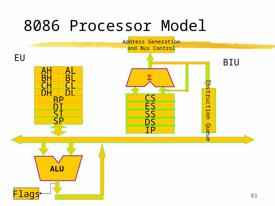
8086 Processor Model
BH BLAH AL
DH DLCH CL
BPDISISP
ALU
Flags
CSESSSDSIP
Address Generationand Bus Control
Instruction Queue
EU BIU
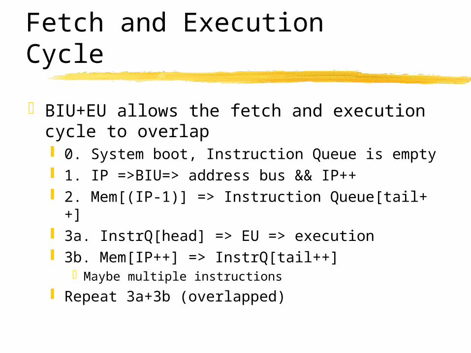
Fetch and Execution Cycle
BIU+EU allows the fetch and execution cycle to overlap 0. System boot, Instruction Queue is empty 1. IP =>BIU=> address bus && IP++ 2. Mem[(IP-1)] => Instruction Queue[tail++] 3a. InstrQ[head] => EU => execution 3b. Mem[IP++] => InstrQ[tail++]
Maybe multiple instructions
Repeat 3a+3b (overlapped)
Waiting Conditions: Memory Access
BIU+EU: execute (almost) continuously without waiting
Waiting Conditions: Accessing memory locations not in queue BIU suspend instruction fetch Issues external memory address Resumes instruction fetch and execution
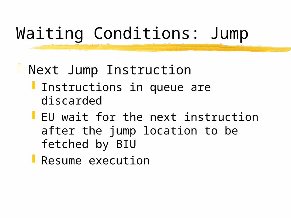
Waiting Conditions: Jump
Next Jump Instruction Instructions in queue are discarded EU wait for the next instruction after the jump
location to be fetched by BIU Resume execution
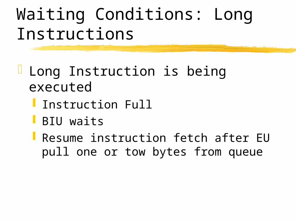
Waiting Conditions: Long Instructions
Long Instruction is being executed Instruction Full BIU waits Resume instruction fetch after EU pull one or tow
bytes from queue
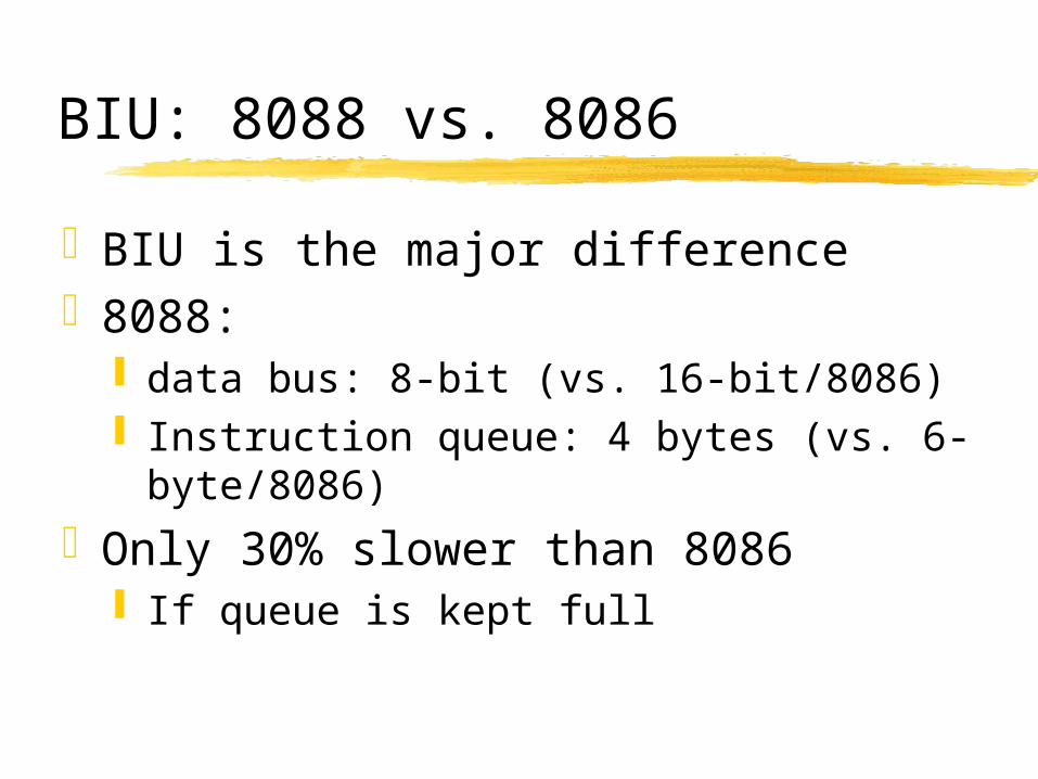
BIU: 8088 vs. 8086
BIU is the major difference8088:
data bus: 8-bit (vs. 16-bit/8086) Instruction queue: 4 bytes (vs. 6-byte/8086)
Only 30% slower than 8086 If queue is kept full
89
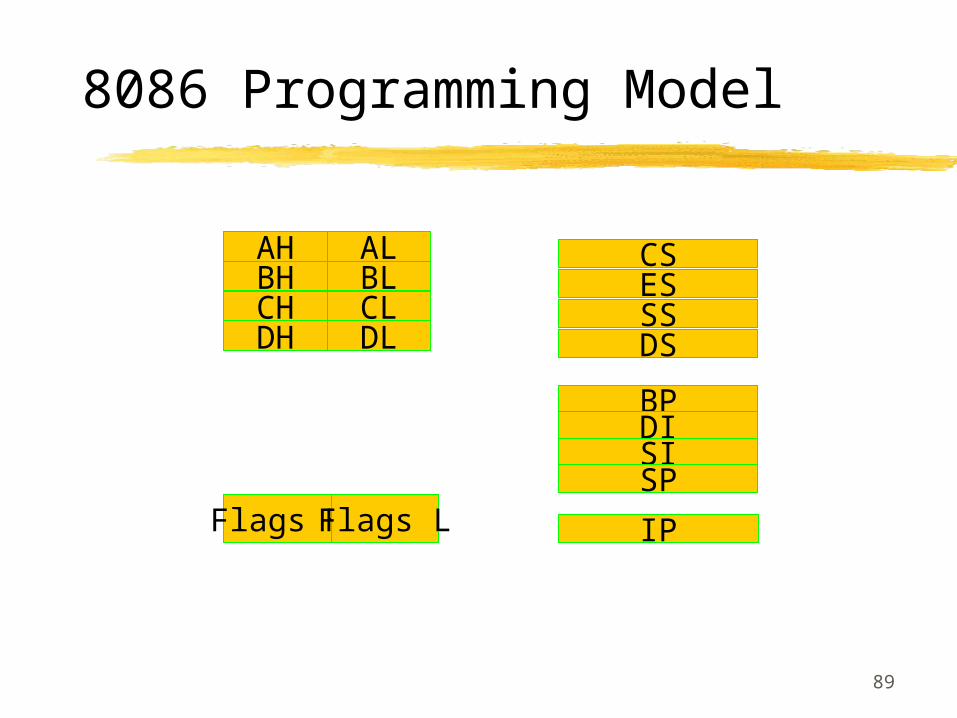
8086 Programming Model
BH BLAH AL
DH DLCH CL
BPDISISP
CSESSSDS
IPFlags H Flags L
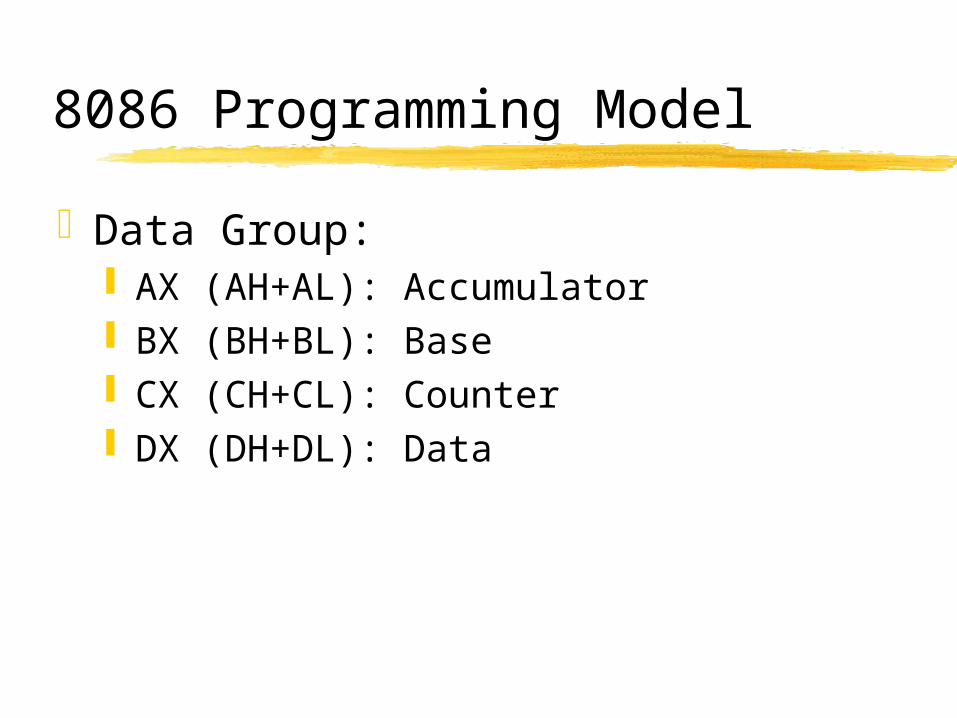
8086 Programming Model
Data Group: AX (AH+AL): Accumulator BX (BH+BL): Base CX (CH+CL): Counter DX (DH+DL): Data
8086 Programming Model
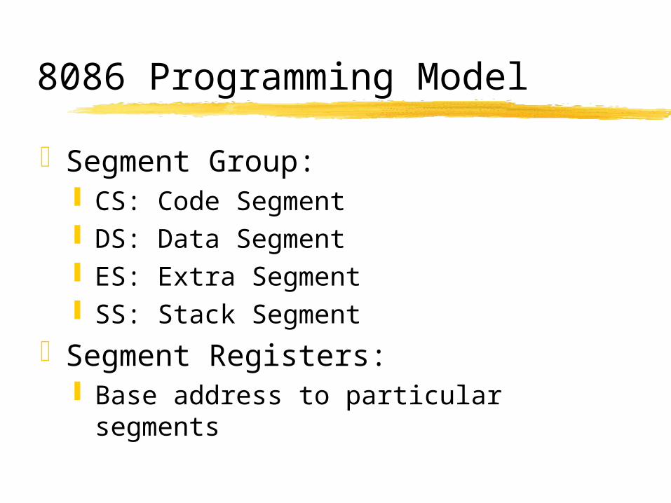
Segment Group: CS: Code Segment DS: Data Segment ES: Extra Segment SS: Stack Segment
Segment Registers: Base address to particular segments
8086 Programming Model
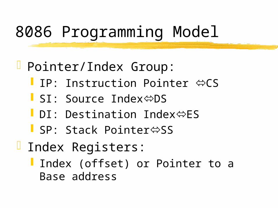
Pointer/Index Group: IP: Instruction Pointer CS SI: Source IndexDS DI: Destination IndexES SP: Stack PointerSS
Index Registers: Index (offset) or Pointer to a Base address
8086 8086 Flag WordFlag Word
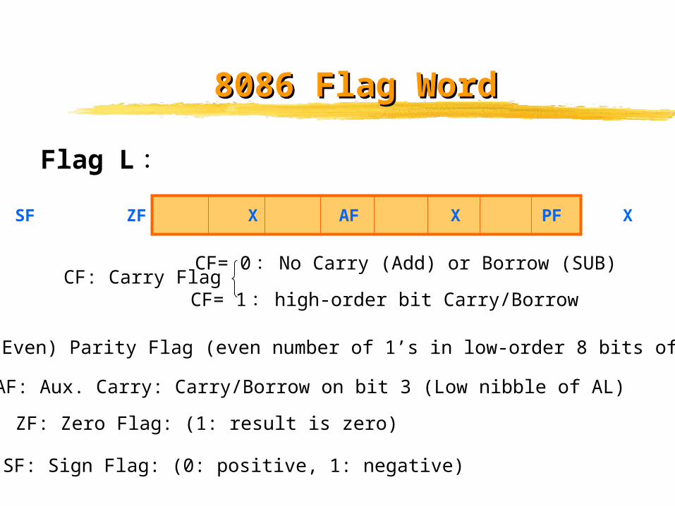
Flag L :
SF ZF X AF X PF X CF
CF: Carry FlagCF= 0 : No Carry (Add) or Borrow (SUB)
CF= 1 : high-order bit Carry/Borrow
AF: Aux. Carry: Carry/Borrow on bit 3 (Low nibble of AL)
SF: Sign Flag: (0: positive, 1: negative)
ZF: Zero Flag: (1: result is zero)
PF: (Even) Parity Flag (even number of 1’s in low-order 8 bits of result)
8086 8086 Flag WordFlag Word
Flag H :
X X X X OF DF IF TF
TF: Trap flag (single-step after next instruction; clear by single-step interrupt)
IF: Interrupt-Enable: enable maskable interrupts
DF: Direction flag: auto-decrement (1) or increment(0) index on string operations
OF: Overflow: signed result cannot be expressed within #bits in destination operand
Segmented Memory
Linear vs. Segmented Linear Addressing:
The entire memory is regarded as a wholethe entire memory space is available all the time
Segmented:memory is divided into segmentsProcess is limited to access designated segments at a
given time
8086 Memory Organization
Even and Odd Memory Banks 16-bit data bustwo-byte / two one-byte access Allows processor to work on bytes or on words
(16-bit)IO operations are normally conducted in bytes
Can handle odd-length instructionsSingle byte instructionsMultiple byte (and very long) instructions
8086 Memory Organization
Memory Space: 20-bit address bus Linearly, 1M bytes directly addressable
Memory Banks Can read 16-bit data (512K words) from even and
odd-addressed simultaneouslyneed Two memory banks in parallelBHE control line: allows addressing even/odd banks
or both
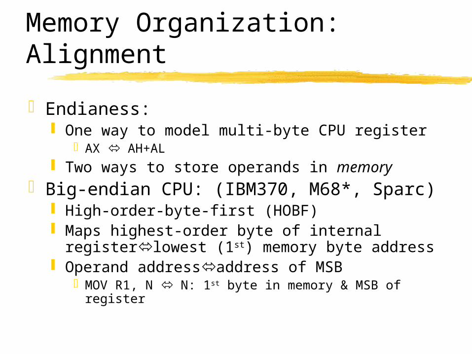
Memory Organization: Alignment
Endianess: One way to model multi-byte CPU register
AX AH+AL Two ways to store operands in memory
Big-endian CPU: (IBM370, M68*, Sparc) High-order-byte-first (HOBF) Maps highest-order byte of internal registerlowest (1st)
memory byte address Operand addressaddress of MSB
MOV R1, N N: 1st byte in memory & MSB of register
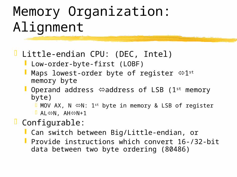
Memory Organization: Alignment
Little-endian CPU: (DEC, Intel) Low-order-byte-first (LOBF) Maps lowest-order byte of register 1st memory byte Operand address address of LSB (1st memory byte)
MOV AX, N N: 1st byte in memory & LSB of registerALN, AHN+1
Configurable: Can switch between Big/Little-endian, or Provide instructions which convert 16-/32-bit data between
two byte ordering (80486)
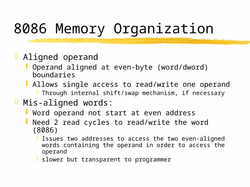
8086 Memory Organization
Aligned operand Operand aligned at even-byte (word/dword) boundaries Allows single access to read/write one operand
Through internal shift/swap mechanism, if necessary
Mis-aligned words: Word operand not start at even address Need 2 read cycles to read/write the word (8086)
Issues two addresses to access the two even-aligned words containing the operand in order to access the operand
slower but transparent to programmer
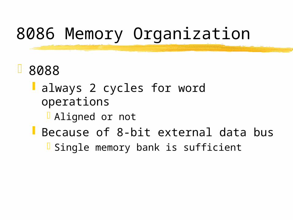
8086 Memory Organization
8088 always 2 cycles for word operations
Aligned or not
Because of 8-bit external data busSingle memory bank is sufficient
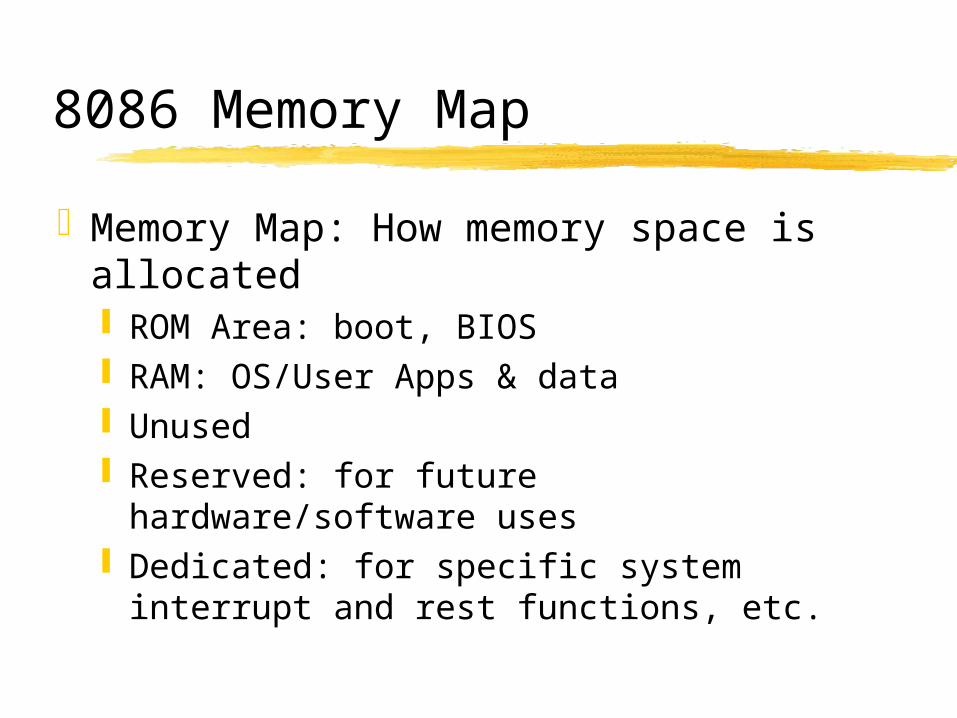
8086 Memory Map
Memory Map: How memory space is allocated ROM Area: boot, BIOS RAM: OS/User Apps & data Unused Reserved: for future hardware/software uses Dedicated: for specific system interrupt and rest
functions, etc.
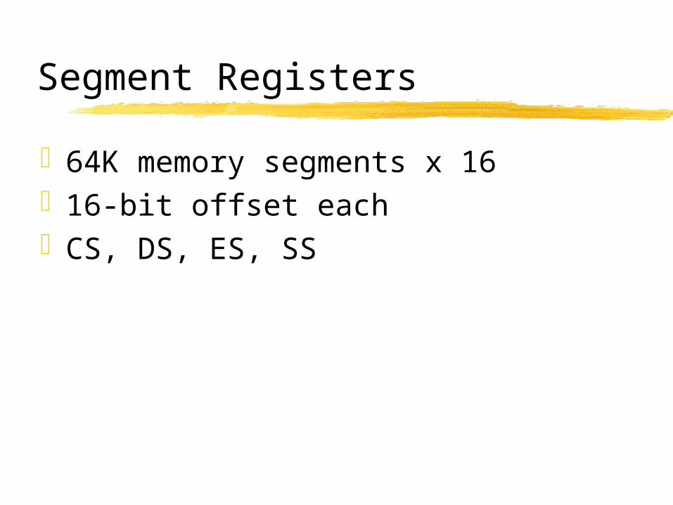
Segment Registers
64K memory segments x 1616-bit offset eachCS, DS, ES, SS
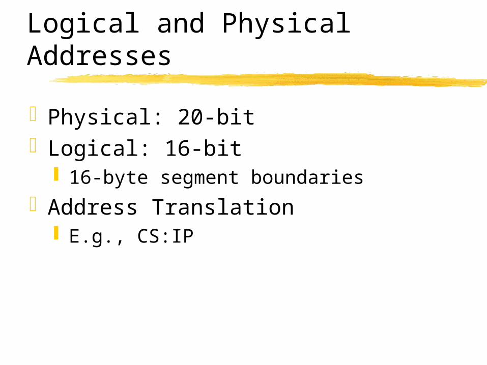
Logical and Physical Addresses
Physical: 20-bitLogical: 16-bit
16-byte segment boundaries
Address Translation E.g., CS:IP
80286
First with Protection ModeReview of 286 Protected Mode … Next

80286
Became available in 1982used in IBM AT computer (1984)16-bit data busclock speed 25% faster than 8088, throughput
5 times greater than 808824-bit address bus (16 MB) (vs. 20-bit/1M
8086)
80286: Real vs. Protected Modes
Larger address space: 24-bit address bus Real Mode vs. Protected Mode
Real Mode: Power on default mode Function like a 8086: use 20-bit least significant address
lines (1M) Software compatible with 286 16 new instructions (for Protected Mode management) Faster 286: redesigned processor, plus higher clock rate (6-
8MHz)
80286: Real vs. Protected Modes
Protected Mode: Multi-program environment Each program has a predetermined amount of
memory Addressed via segment selector (physical
addresses invisible): 16M addressable Multiple programs loaded at once (within their
respective segments), protected from read/write by each other

80286: Real vs. Protected Modes
Protected Mode: Cannot be switch back to real mode to avoid
illegal access by switching back and forth between modes
A faster 8086 only? MS-DOS requires that all programs be run in Real
Mode
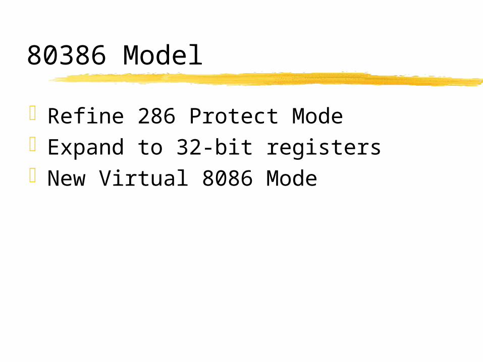
80386 Model
Refine 286 Protect ModeExpand to 32-bit registersNew Virtual 8086 Mode

80386 Review
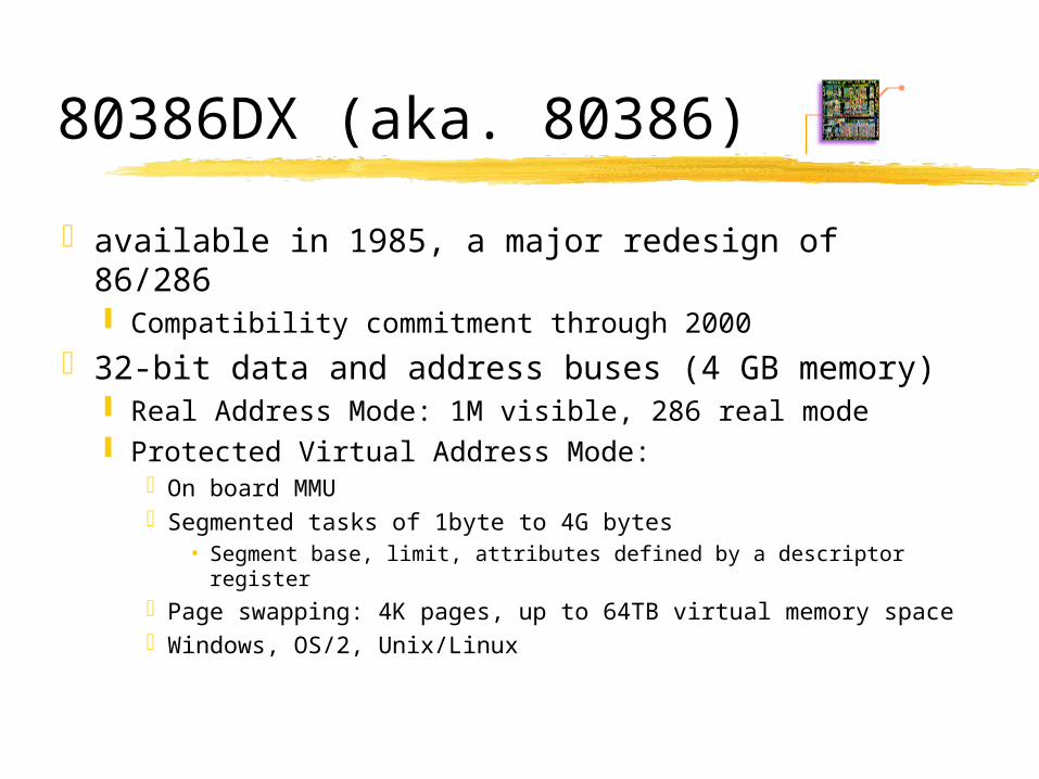
80386DX (aka. 80386)
available in 1985, a major redesign of 86/286 Compatibility commitment through 2000
32-bit data and address buses (4 GB memory) Real Address Mode: 1M visible, 286 real mode Protected Virtual Address Mode:
On board MMUSegmented tasks of 1byte to 4G bytes
• Segment base, limit, attributes defined by a descriptor register
Page swapping: 4K pages, up to 64TB virtual memory spaceWindows, OS/2, Unix/Linux
80386DX (aka. 80386)
Virtual 8086 mode (a special Protected mode feature): permitted multiple 8086 virtual machines-multitasking (similar to real mode) Windows (multiple MSDOS’s)
Clock rate: max. 40MHz, 2 pulses per R/W bus cycle External memory cache to avoid wait
Fast SRAM93% hit rate with 64K cache
Compatible instructions (14 new)

80386SX
80386SX: (for transition to 32-bit) 16-bit data bus/32-bit register 24-bit address bus
80386: Real vs. Protected Modes
Larger address space: 32-bit address bus (4G) Real Mode vs. Protected Mode (refined from 286)
Real Mode: Power on default mode Function like a 8086: (1) use only 20-bit least significant
address lines (1M) (2) segmented memory retained (64K) Software compatible with 286
New Real Mode Features: access to 32-bit register set two new segments: F, G
80386: Real vs. Protected Modes
Protected Mode: new addressing mechanism vs. real mode supports protection levels segment size: 1 to 4G (not 64K, fixed) segment register: pointer to a descriptor table
not base address
80386: Real vs. Protected Modes
Protected Mode: descriptor table: (8 byte per entry)
32-bit base address of segmentsegment sizeaccess rights
memory address = base address (in table) + offset (in instruction)
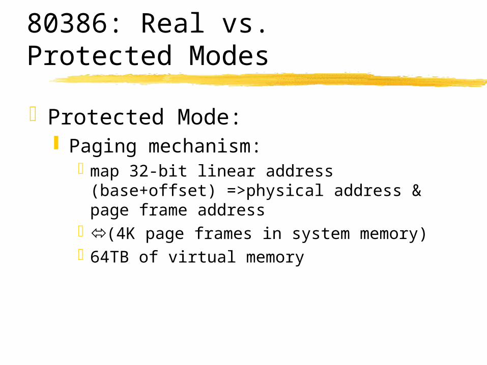
80386: Real vs. Protected Modes
Protected Mode: Paging mechanism:
map 32-bit linear address (base+offset) =>physical address & page frame address
(4K page frames in system memory)64TB of virtual memory
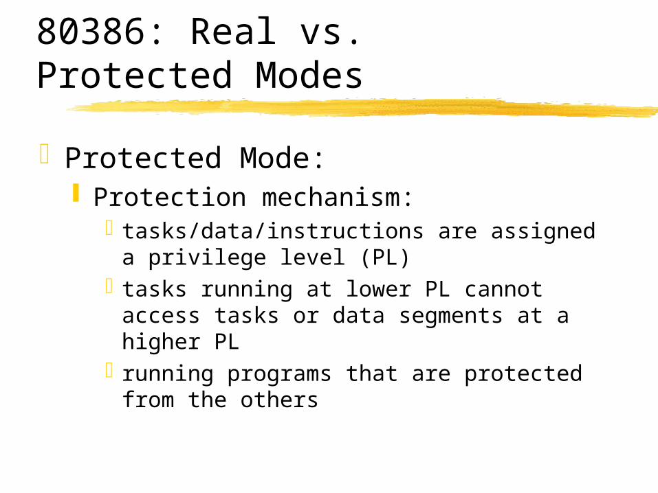
80386: Real vs. Protected Modes
Protected Mode: Protection mechanism:
tasks/data/instructions are assigned a privilege level (PL)
tasks running at lower PL cannot access tasks or data segments at a higher PL
running programs that are protected from the others
80386: Real vs. Protected Modes
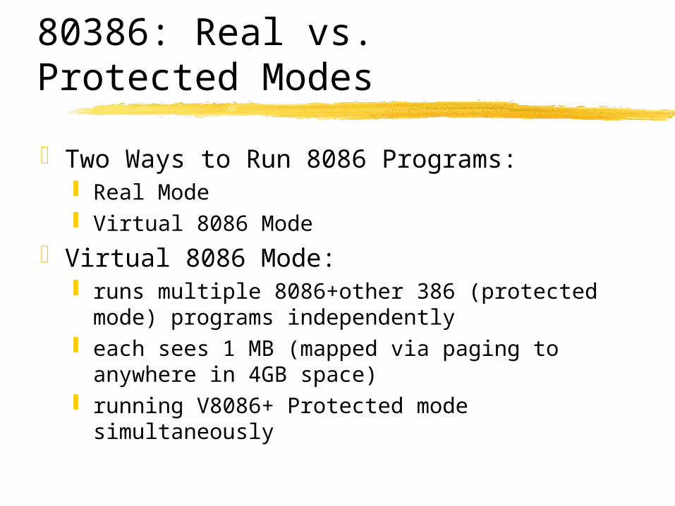
Two Ways to Run 8086 Programs: Real Mode Virtual 8086 Mode
Virtual 8086 Mode: runs multiple 8086+other 386 (protected mode) programs
independently each sees 1 MB (mapped via paging to anywhere in 4GB
space) running V8086+ Protected mode simultaneously
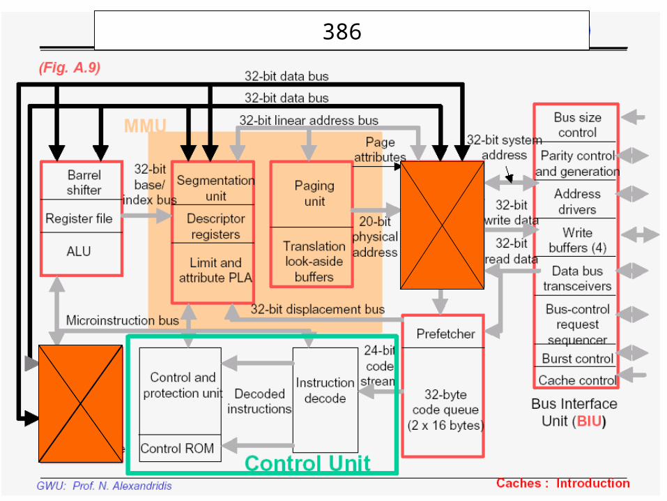
80386 Processor Model386
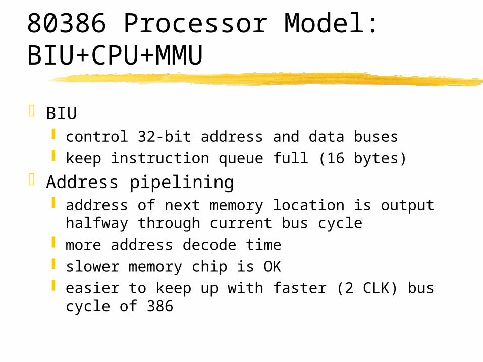
80386 Processor Model: BIU+CPU+MMU
BIU control 32-bit address and data buses keep instruction queue full (16 bytes)
Address pipelining address of next memory location is output halfway through
current bus cycle more address decode time slower memory chip is OK easier to keep up with faster (2 CLK) bus cycle of 386
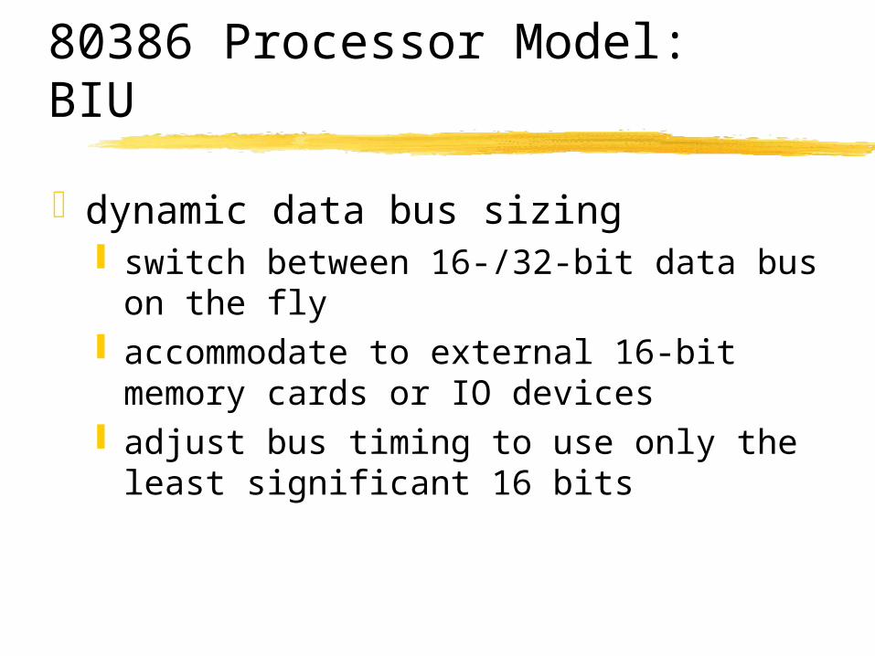
80386 Processor Model: BIU
dynamic data bus sizing switch between 16-/32-bit data bus on the fly accommodate to external 16-bit memory cards or
IO devices adjust bus timing to use only the least significant
16 bits
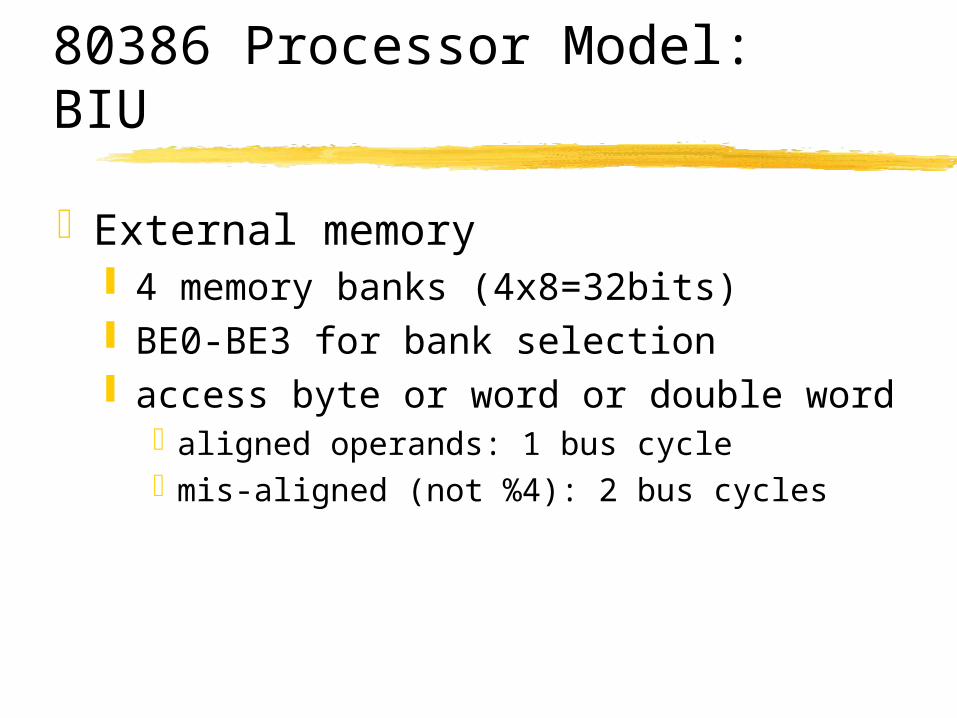
80386 Processor Model: BIU
External memory 4 memory banks (4x8=32bits) BE0-BE3 for bank selection access byte or word or double word
aligned operands: 1 bus cyclemis-aligned (not %4): 2 bus cycles
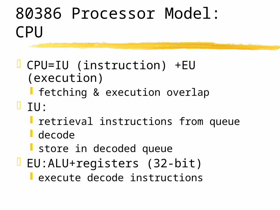
80386 Processor Model: CPU
CPU=IU (instruction) +EU (execution) fetching & execution overlap
IU: retrieval instructions from queue decode store in decoded queue
EU:ALU+registers (32-bit) execute decode instructions
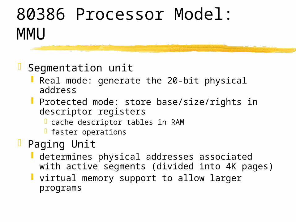
80386 Processor Model: MMU
Segmentation unit Real mode: generate the 20-bit physical address Protected mode: store base/size/rights in descriptor
registerscache descriptor tables in RAMfaster operations
Paging Unit determines physical addresses associated with active
segments (divided into 4K pages) virtual memory support to allow larger programs
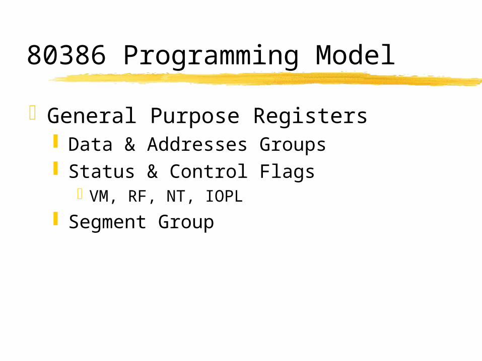
80386 Programming Model
General Purpose Registers Data & Addresses Groups Status & Control Flags
VM, RF, NT, IOPL
Segment Group
80386 Programming Model
Special purpose Registers
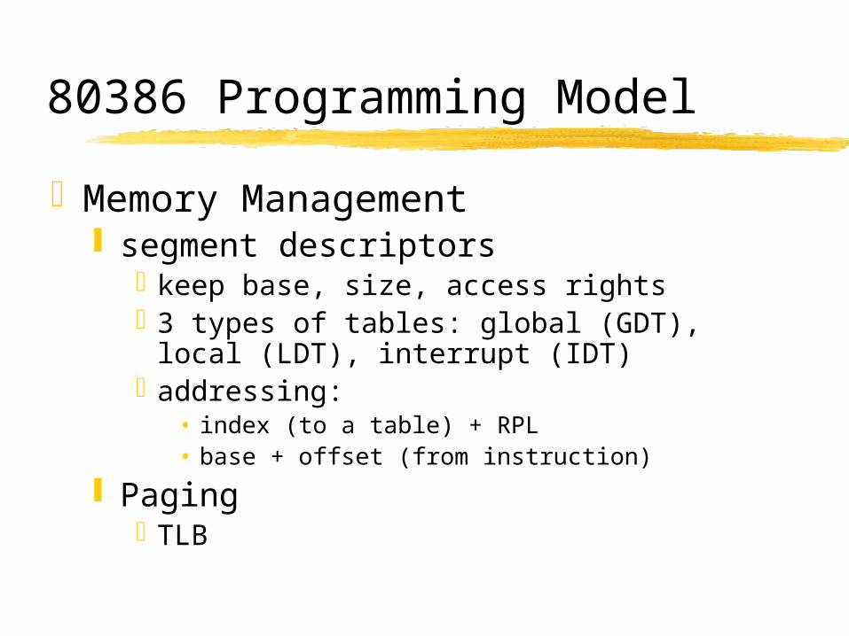
80386 Programming Model
Memory Management segment descriptors
keep base, size, access rights3 types of tables: global (GDT), local (LDT), interrupt
(IDT)addressing:
• index (to a table) + RPL• base + offset (from instruction)
PagingTLB
80386 Programming Model
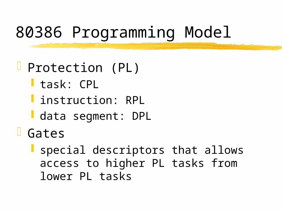
Protection (PL) task: CPL instruction: RPL data segment: DPL
Gates special descriptors that allows access to higher PL
tasks from lower PL tasks

80486 Review …

80486DX
1989: a polished 386, 6 new OS level instructionsvirtually identical to 386 in terms of compatibilityRISC design concepts
fewer clock cycles per operation, a single clock cycle for most frequently used instructions
Max 50MHz 5 stage execution pipeline
Portions of 5 instructions execute at once

80486DX
Highly Integrated: On board 8K memory cache FPP (equivalent to external 80387 co-processor)
Twice as fast as 386 at any given clock rate 20Mhz 486 ~= 40Mhz 386
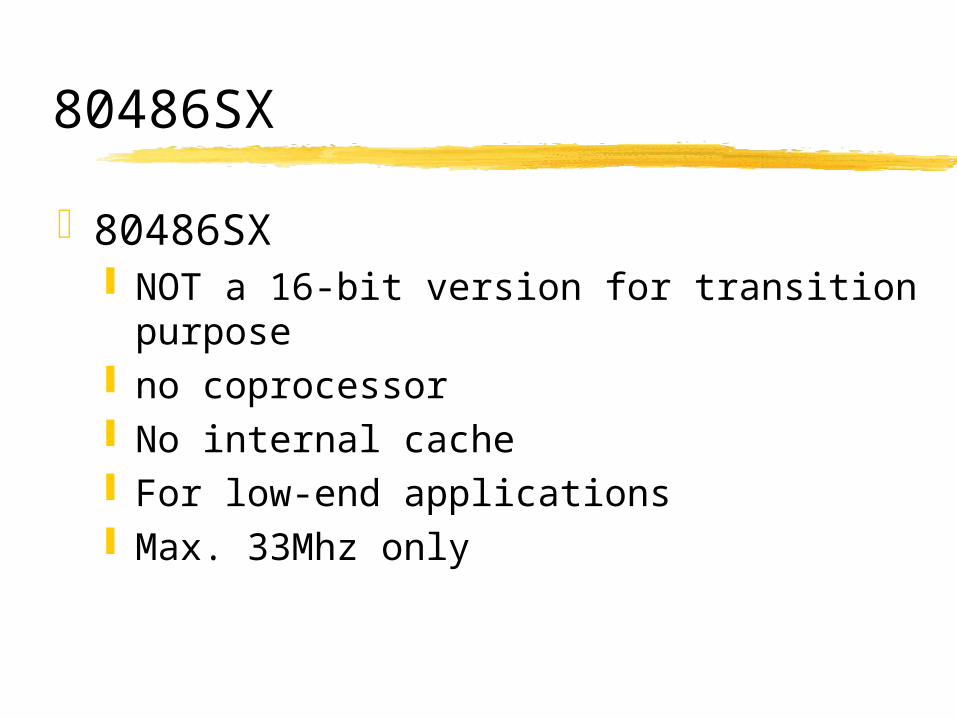
80486SX
80486SX NOT a 16-bit version for transition purpose no coprocessor No internal cache For low-end applications Max. 33Mhz only
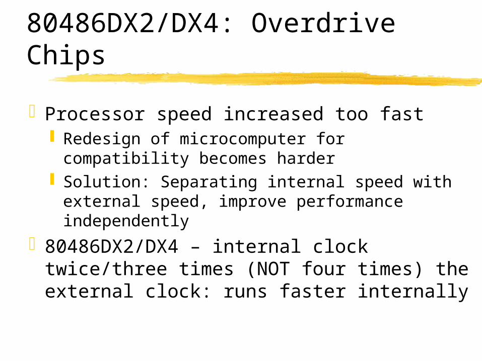
80486DX2/DX4: Overdrive Chips
Processor speed increased too fast Redesign of microcomputer for compatibility
becomes harder Solution: Separating internal speed with external
speed, improve performance independently
80486DX2/DX4 – internal clock twice/three times (NOT four times) the external clock: runs faster internally
80486DX2/DX4: Overdrive Chips
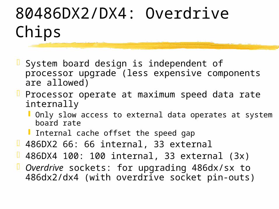
System board design is independent of processor upgrade (less expensive components are allowed)
Processor operate at maximum speed data rate internally Only slow access to external data operates at system board rate Internal cache offset the speed gap
486DX2 66: 66 internal, 33 external486DX4 100: 100 internal, 33 external (3x)Overdrive sockets: for upgrading 486dx/sx to
486dx2/dx4 (with overdrive socket pin-outs)
486 Processor Features
386 features: Real/Protected Modes Memory Management PL’s registers & bus sizes
New features 6 OS instructions 8K/16K onboard cache (was external before 386)
486 Processor Features
A better 386 5 stage instruction pipeline
IF/ID/EX => PF/D1/D2/EX/WBPF: instructions => Q (2*16-bytes)D1: determine opcodeD2: determine memory address of operandsEX: execute indicated OPWB: update register
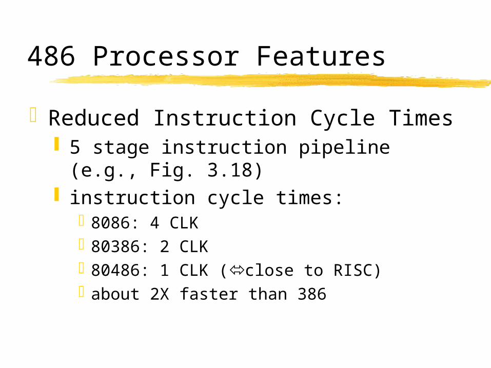
486 Processor Features
Reduced Instruction Cycle Times 5 stage instruction pipeline (e.g., Fig. 3.18) instruction cycle times:
8086: 4 CLK80386: 2 CLK80486: 1 CLK (close to RISC)about 2X faster than 386
486 Processor Model: 386+FPU+Cache
386 units retained: BIU, CPU, MMUnew: FPU (80387) + Cache (8K/16K)FPU:
387 onboard0.8 u => #transistors increased (275K => 1+ millions)simplified system board designspeedup FP operations
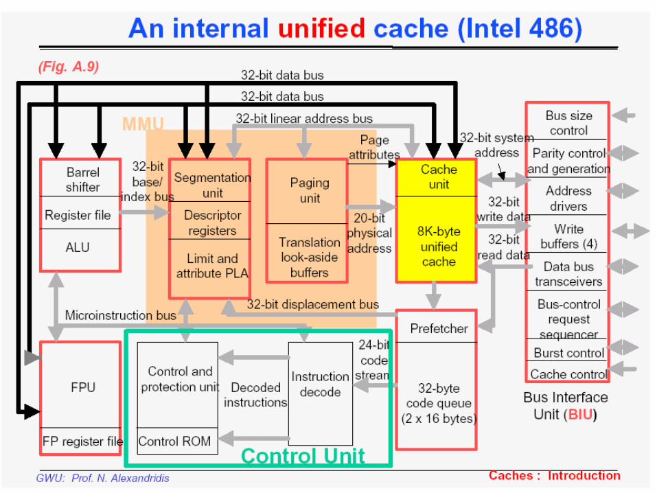
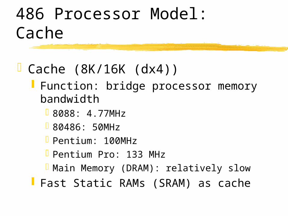
486 Processor Model: Cache
Cache (8K/16K (dx4)) Function: bridge processor memory bandwidth
8088: 4.77MHz80486: 50MHzPentium: 100MHzPentium Pro: 133 MHzMain Memory (DRAM): relatively slow
Fast Static RAMs (SRAM) as cache
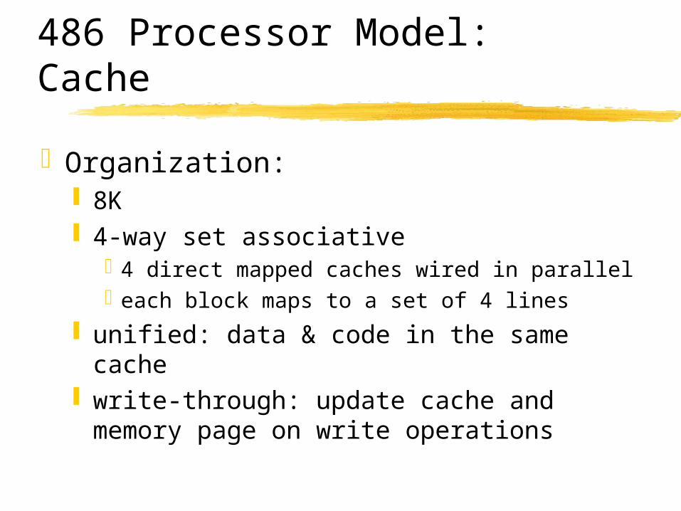
486 Processor Model: Cache
Organization: 8K 4-way set associative
4 direct mapped caches wired in paralleleach block maps to a set of 4 lines
unified: data & code in the same cache write-through: update cache and memory page on
write operations
486 Processor Model: Cache
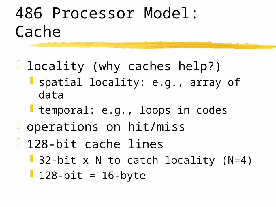
locality (why caches help?) spatial locality: e.g., array of data temporal: e.g., loops in codes
operations on hit/miss128-bit cache lines
32-bit x N to catch locality (N=4) 128-bit = 16-byte
486 Processor Model: Cache
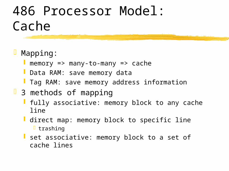
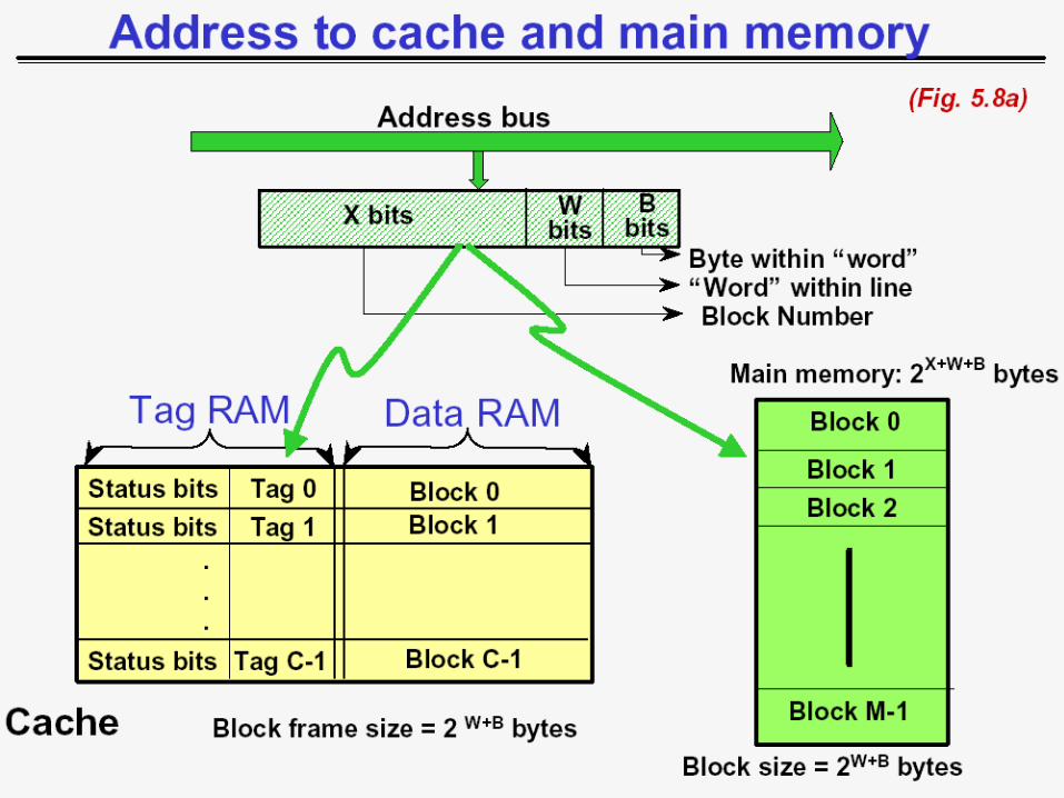
Mapping: memory => many-to-many => cache Data RAM: save memory data Tag RAM: save memory address information
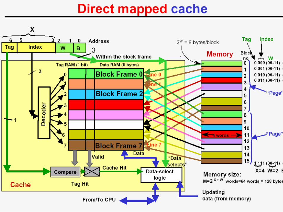
3 methods of mapping fully associative: memory block to any cache line direct map: memory block to specific line
trashing
set associative: memory block to a set of cache lines
486 Processor Model: Cache
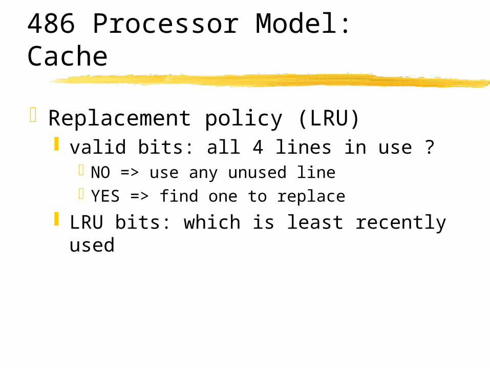
Replacement policy (LRU) valid bits: all 4 lines in use ?
NO => use any unused lineYES => find one to replace
LRU bits: which is least recently used

Pentium Review …
Pentium: Superscaler Processor
available in 199232-bit architectureSuperscaler architecture
Scaling: scaling down etchable feature size to increase complexity of IC (e.g., DRAM)
10 microns/4004 to 0.13 microns (2001) Superscaler: go beyond simply scaling down Two instruction pipelines: each with own ALU, address
generation circuitry, data cache interface Execute two different instructions simultaneously

Pentium: Superscaler Processor
Onboard cache Separate 8K data and code caches to avoid access
conflictsFPPInstruction pipeline: 8 stageOptimized floating point functions
5x-10x FLOP’s of 486 2x performance of 486 at any clock rate

Pentium: Superscaler Processor
Compatibility with 386/486: Internal 32-bit registers and address bus Data bus expanded to 64-bits for higher data
transfer rateCompare 8088 to 386sx transition

Pentium: Superscaler Processor
non-clone competition from AMD, Cyrixdevelopment of brand identity by Intel

Pentium Pro Review …

Pentium Pro: Two Chips in One
Became available in 1995Superscaler of degree 3
Can execute 3 instructions simultaneously
Optimized for 32-bit operating systems (e.g., Windows NT, OS2/Warp)
Two separate silicon die on the same package Processor: 0.35 u, 5.5 million transistors 256KB(/512K) Level 2 cache included on chip, 15.5
million transistors in smaller area

Pentium Pro: Two Chips in One
On Board Level 2 cache Simplifies system board design Requires less space Gains faster communication with processor
Internal (level 1) cache: 8KPentium Pro 133 ~= 2x Pentium 66 ~= 4x
486DX2 66
Pentium Pro:Dynamic Execution
Dynamic execution: reduce idle processor time by predicting instruction behaviors Multiple Branch Prediction: look as far as 30 instructions
ahead to anticipate program branches Data Flow Analysis: looks at upcoming instructions and
determine if they are available for processing, depending on other instructions. Determine optimal execution sequences.
Speculative Execution: execute instructions in different order as entered. Speculative results are stored until final states can be determined.