Embed Size (px)
Citation preview
Chapter 6Main Memory Scaling:Challenges and Solution DirectionsOnur Mutlu, Carnegie Mellon University
AbstractThe memory system is a fundamental performance and energy bottleneck in al-
most all computing systems. Recent system design, application, and technologytrends that require more capacity, bandwidth, efficiency, and predictability out ofthe memory system make it an even more important system bottleneck. At the sametime, DRAM technology is experiencing difficult technology scaling challenges thatmake the maintenance and enhancement of its capacity, energy-efficiency, and reli-ability significantly more costly with conventional techniques.
In this chapter, after describing the demands and challenges faced by the mem-ory system, we examine some promising research and design directions to over-come challenges posed by memory scaling. Specifically, we describe three majorsolution directions: 1) enabling new DRAM architectures, functions, interfaces, andbetter integration of the DRAM and the rest of the system (an approach we callsystem-DRAM co-design), 2) designing a memory system that employs emergingnon-volatile memory technologies and takes advantage of multiple different tech-nologies (i.e., hybrid memory systems), 3) providing predictable performance andQoS to applications sharing the memory system (i.e., QoS-aware memory systems).We also briefly describe our ongoing related work in combating scaling challengesof NAND flash memory.
6.1 Introduction
Main memory is a critical component of all computing systems, employed in server,embedded, desktop, mobile and sensor environments. Memory capacity, energy,cost, performance, and management algorithms must scale as we scale the size ofthe computing system in order to maintain performance growth and enable new ap-plications. Unfortunately, such scaling has become difficult because recent trends insystems, applications, and technology greatly exacerbate the memory system bot-tleneck.
v
vi 6 Main Memory Scaling: Challenges and Solution Directions
6.2 Trends: Systems, Applications, Technology
In particular, on the systems/architecture front, energy and power consumption havebecome key design limiters as the memory system continues to be responsible fora significant fraction of overall system energy/power [69]. More and increasinglyheterogeneous processing cores and agents/clients are sharing the memory sys-tem [6, 21, 107, 45, 46, 36, 23], leading to increasing demand for memory capacityand bandwidth along with a relatively new demand for predictable performance andquality of service (QoS) from the memory system [81, 87, 106].
On the applications front, important applications are usually very data intensiveand are becoming increasingly so [8], requiring both real-time and offline manipu-lation of great amounts of data. For example, next-generation genome sequencingtechnologies produce massive amounts of sequence data that overwhelms mem-ory storage and bandwidth requirements of today’s high-end desktop and laptopsystems [109, 4, 115] yet researchers have the goal of enabling low-cost personal-ized medicine. Creation of new killer applications and usage models for computerslikely depends on how well the memory system can support the efficient storage andmanipulation of data in such data-intensive applications. In addition, there is an in-creasing trend towards consolidation of applications on a chip to improve efficiency,which leads to the sharing of the memory system across many heterogeneous appli-cations with diverse performance requirements, exacerbating the aforementionedneed for predictable performance guarantees from the memory system [106, 108].
On the technology front, two major trends profoundly affect memory systems.First, there is increasing difficulty scaling the well-established charge-based mem-ory technologies, such as DRAM [77, 53, 40, 5, 62, 1] and flash memory [59, 76,10, 11, 14], to smaller technology nodes. Such scaling has enabled memory sys-tems with reasonable capacity and efficiency; lack of it will make it difficult toachieve high capacity and efficiency at low cost. Second, some emerging resistivememory technologies, such as phase change memory (PCM) [100, 113, 62, 63, 98],spin-transfer torque magnetic memory (STT-MRAM) [19, 60] or resistive RAM(RRAM) [114] appear more scalable, have latency and bandwidth characteristicsmuch closer to DRAM than flash memory and hard disks, and are non-volatile withlittle idle power consumption. Such emerging technologies can enable new oppor-tunities in system design, including, for example, the unification of memory andstorage subsystems [80]. They have the potential to be employed as part of mainmemory, alongside or in place of less scalable and leaky DRAM, but they also havevarious shortcomings depending on the technology (e.g., some have cell enduranceproblems, some have very high write latency/power, some have low density) thatneed to be overcome or tolerated.
6.3 Requirements: Traditional and New vii
6.3 Requirements: Traditional and New
System architects and users have always wanted more from the memory system:high performance (ideally, zero latency and infinite bandwidth), infinite capacity, allat zero cost! The aforementioned trends do not only exacerbate and morph the aboverequirements, but also add some new requirements. We classify the requirementsfrom the memory system into two categories: exacerbated traditional requirementsand (relatively) new requirements.
The traditional requirements of performance, capacity, and cost are greatly ex-acerbated today due to increased pressure on the memory system, consolidation ofmultiple applications/agents sharing the memory system, and difficulties in DRAMtechnology and density scaling. In terms of performance, two aspects have changed.First, today’s systems and applications not only require low latency and high band-width (as traditional memory systems have been optimized for), but they also re-quire new techniques to manage and control memory interference between differentcores, agents, and applications that share the memory system [81, 87, 106, 26, 108]in order to provide high system performance as well as predictable performance (orquality of service) to different applications [106]. Second, there is a need for in-creased memory bandwidth for many applications as the placement of more coresand agents on chip make the memory pin bandwidth an increasingly precious re-source that determines system performance [41], especially for memory-bandwidth-intensive workloads, such as GPGPUs [48, 47], heterogeneous systems [6], and con-solidated workloads [87, 44, 43]. In terms of capacity, the need for memory capacityis greatly increasing due to the placement of multiple data-intensive applications onthe same chip and continued increase in the data sets of important applications. Onerecent work showed that given that the core count is increasing at a faster rate thanDRAM capacity, the expected memory capacity per core is to drop by 30% everytwo years [70], an alarming trend since much of today’s software innovations andfeatures rely on increased memory capacity. In terms of cost, increasing difficultyin DRAM technology scaling poses a difficult challenge to building higher density(and, as a result, lower cost) main memory systems. Similarly, cost-effective op-tions for providing high reliability and increasing memory bandwidth are neededto scale the systems proportionately with the reliability and data throughput needsof today’s data-intensive applications. Hence, the three traditional requirements ofperformance, capacity, and cost have become exacerbated.
The relatively new requirements from the main memory system are threefold.First, technology scalability: there is a new need for finding a technology that ismuch more scalable than DRAM in terms of capacity, energy, and cost, as describedearlier. As DRAM continued to scale well from the above-100-nm to 30-nm tech-nology nodes, the need for finding a more scalable technology was not a prevalentproblem. Today, with the significant circuit and device scaling challenges DRAMhas been facing below the 30-nm node, it is. Second, there is a relatively new needfor providing performance predictability and QoS in the shared main memory sys-tem. As single-core systems were dominant and memory bandwidth and capacitywere much less of a shared resource in the past, the need for predictable perfor-
viii 6 Main Memory Scaling: Challenges and Solution Directions
mance was much less apparent or prevalent [81]. Today, with increasingly morecores/agents on chip sharing the memory system and increasing amounts of work-load consolidation, memory fairness, predictable memory performance, and tech-niques to mitigate memory interference have become first-class design constraints.Third, there is a great need for much higher energy/power/bandwidth efficiency inthe design of the main memory system. Higher efficiency in terms of energy, power,and bandwidth enables the design of much more scalable systems where main mem-ory is shared between many agents, and can enable new applications in almost alldomains where computers are used. Arguably, this is not a new need today, but webelieve it is another first-class design constraint that has not been as traditional asperformance, capacity, and cost.
6.4 Solution Directions
As a result of these systems, applications, and technology trends and the resultingrequirements, it is our position that researchers and designers need to fundamen-tally rethink the way we design memory systems today to 1) overcome scaling chal-lenges with DRAM, 2) enable the use of emerging memory technologies, 3) designmemory systems that provide predictable performance and quality of service to ap-plications and users. The rest of this chapter describes our solution ideas in thesethree directions, with pointers to specific techniques when possible. Since scalingchallenges themselves arise due to difficulties in enhancing memory components atsolely one level of the computing stack (e.g., the device and/or circuit levels in caseof DRAM scaling), we believe effective solutions to the above challenges will re-quire cooperation across different layers of the computing stack, from algorithms tosoftware to microarchitecture to devices, as well as between different componentsof the system, including processors, memory controllers, memory chips, and thestorage subsystem. As much as possible, we will give examples of such solutionsand directions.
6.5 Challenge 1: New DRAM Architectures
DRAM has been the choice technology for implementing main memory due to itsrelatively low latency and low cost. DRAM process technology scaling has for longenabled lower cost per unit area by enabling reductions in DRAM cell size. Unfor-tunately, further scaling of DRAM cells has become costly [5, 77, 53, 40, 62, 1] dueto increased manufacturing complexity/cost, reduced cell reliability, and potentiallyincreased cell leakage leading to high refresh rates. Several key issues to tackle in-clude:
1) reducing the negative impact of refresh on energy, performance, QoS, anddensity scaling [71, 72, 17],
6.5 Challenge 1: New DRAM Architectures ix
2) improving DRAM parallelism/bandwidth [57, 17], latency [68], and energyefficiency [57, 68, 71],
3) improving reliability of DRAM at low cost [90, 75, 58, 51],4) reducing the significant amount of waste present in today’s main memories
in which much of the fetched/stored data can be unused due to coarse-granularitymanagement [79, 117, 94, 95, 110],
5) minimizing data movement between DRAM and processing elements, whichcauses high latency, energy, and bandwidth consumption [102].
Traditionally, DRAM devices have been separated from the rest of the systemwith a rigid interface, and DRAM has been treated as a passive slave device thatsimply responds to the commands given to it by the memory controller. We believethe above key issues can be solved more easily if we rethink the DRAM architec-ture and functions, and redesign the interface such that DRAM, controllers, and pro-cessors closely cooperate. We call this high-level solution approach system-DRAMco-design. We believe key technology trends, e.g., the 3D stacking of memory andlogic [74, 2, 111] and increasing cost of scaling DRAM solely via circuit-level ap-proaches [77, 53, 40], enable such a co-design to become increasingly more feasi-ble. We proceed to provide several examples from our recent research that tackle theproblems of refresh, parallelism, latency, and energy efficiency.
6.5.1 Reducing Refresh Impact and DRAM Error Management
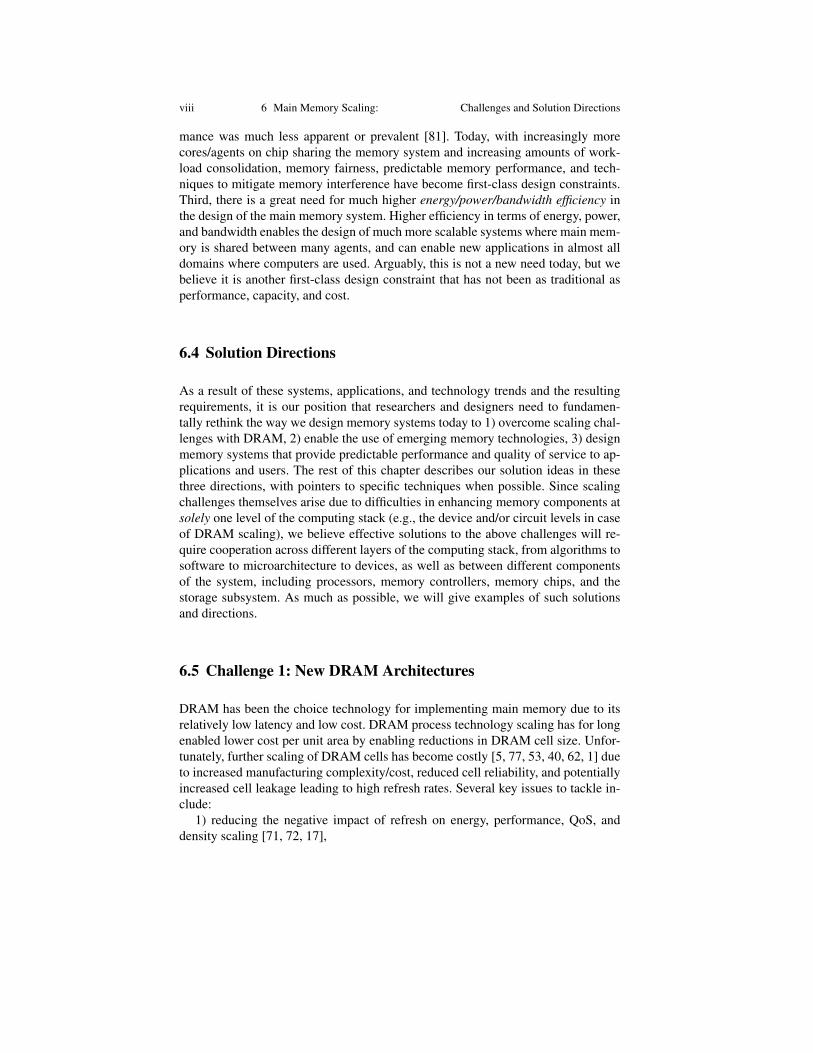
With higher DRAM capacity, more cells need to be refreshed at likely higher ratesthan today. Our recent work [71] indicates that refresh rate limits DRAM densityscaling: a hypothetical 64Gb DRAM device would spend 46% of its time and 47%of all DRAM energy for refreshing its rows, as opposed to typical 4Gb devices of to-day that spend respectively 8% of the time and 15% of the DRAM energy on refresh(as shown in Figure 6.1). Today’s DRAM devices refresh all rows at the same worst-case rate (e.g., every 64ms). However, only a small number of weak rows require ahigh refresh rate [54, 72, 51] (e.g., only ⇠1000 rows in 32GB DRAM require to berefreshed more frequently than every 256ms). Retention-Aware Intelligent DRAMRefresh (RAIDR) [71] exploits this observation: it groups DRAM rows into bins(implemented as Bloom filters [7] to minimize hardware overhead) based on theretention time of the weakest cell within each row. Each row is refreshed at a ratecorresponding to its retention time bin. Since few rows need high refresh rate, onecan use very few bins to achieve large reductions in refresh counts: our results showthat RAIDR with three bins (1.25KB hardware cost) reduces refresh operations by⇠75%, leading to significant improvements in system performance and energy effi-ciency as described by Liu et al. [71].
Like RAIDR, other approaches have also been proposed to take advantage ofthe retention time variation of cells across a DRAM chip. For example, some worksproposed refreshing weak rows more frequently at a per-row granularity, others pro-posed not using memory rows with low retention times, and yet others suggested
x 6 Main Memory Scaling: Challenges and Solution Directions
2 Gb 4 Gb 8 Gb 16 Gb 32 Gb 64 GbDevice capacity
0
20
40
60
80
100
%DRAM
energy
spentrefreshing
Present Future
(a) Power consumption
2 Gb 4 Gb 8 Gb 16 Gb 32 Gb 64 GbDevice capacity
0
20
40
60
80
100
%tim
espentrefreshing
Present Future
(b) Throughput Loss
Fig. 6.1. Impact of refresh in current (DDR3) and projected DRAM devices. Repro-duced from [71].
mapping critical data to cells with longer retention times such that critical data isnot lost [112, 42, 73, 93, 52, 3] – see [71, 72] for a discussion of such techniques.Such approaches that exploit non-uniform retention times across DRAM require ac-curate retention time profiling mechanisms. Understanding of retention time as wellas error behavior of DRAM devices is a critical research topic, which we believecan enable other mechanisms to tolerate refresh impact and errors at low cost. Liuet al. [72] provides an experimental characterization of retention times in modernDRAM devices to aid such understanding. Our initial results in that work, obtainedvia the characterization of 248 modern commodity DRAM chips from five differentDRAM manufacturers, suggest that the retention time of cells in a modern deviceis largely affected by two phenomena: 1) Data Pattern Dependence, where the re-tention time of each DRAM cell is significantly affected by the data stored in otherDRAM cells, 2) Variable Retention Time, where the retention time of a DRAM cellchanges unpredictably over time. These two phenomena pose challenges against ac-curate and reliable determination of the retention time of DRAM cells, online oroffline, and a promising area of future research is to devise techniques that can iden-tify retention times of DRAM cells in the presence of data pattern dependence andvariable retention time. Khan et al.’s recent work [51] provides more analysis ofthe effectiveness of conventional error mitigation mechanisms for DRAM retentionfailures and proposes online retention time profiling as a solution for identifying re-tention times of DRAM cells as a potentially promising approach in future DRAMsystems.
Looking forward, we believe that increasing cooperation between the DRAMdevice and the DRAM controller as well as other parts of the system, includingsystem software, is needed to communicate information about weak (or, unreliable)cells and the characteristics of different rows or physical memory regions from thedevice to the system. The system can then use this information to optimize data al-location and movement, refresh rate management, and error tolerance mechanisms.Low-cost error tolerance mechanisms are likely to be enabled more efficiently withsuch coordination between DRAM and the system. In fact, as DRAM technology
6.5 Challenge 1: New DRAM Architectures xi
scales and error rates increase, it might become increasingly more difficult to main-tain the common illusion that DRAM is a perfect, error-free storage device. DRAMmay start looking increasingly like flash memory, where the memory controllermanages errors such that an acceptable specified uncorrectable bit error rate is sat-isfied [10, 12]. We envision a DRAM Translation Layer (DTL), not unlike the FlashTranslation Layer (FTL) of today in spirit (which is decoupled from the processorand performs a wide variety of management functions for flash memory, includingerror correction, garbage collection, read/write scheduling, etc.), can enable betterscaling of DRAM memory into the future by not only enabling easier error manage-ment but also opening up new opportunities to perform computation and mappingclose to memory. This can become especially feasible in the presence of the trendof combining the DRAM controller and DRAM via 3D stacking. What should theinterface be to such a layer and what should be performed in the DTL are promisingareas of future research.
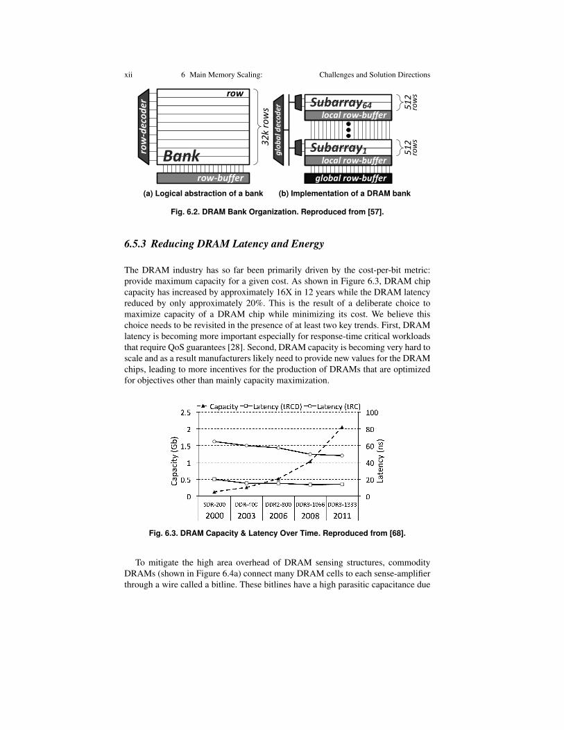
6.5.2 Improving DRAM Parallelism
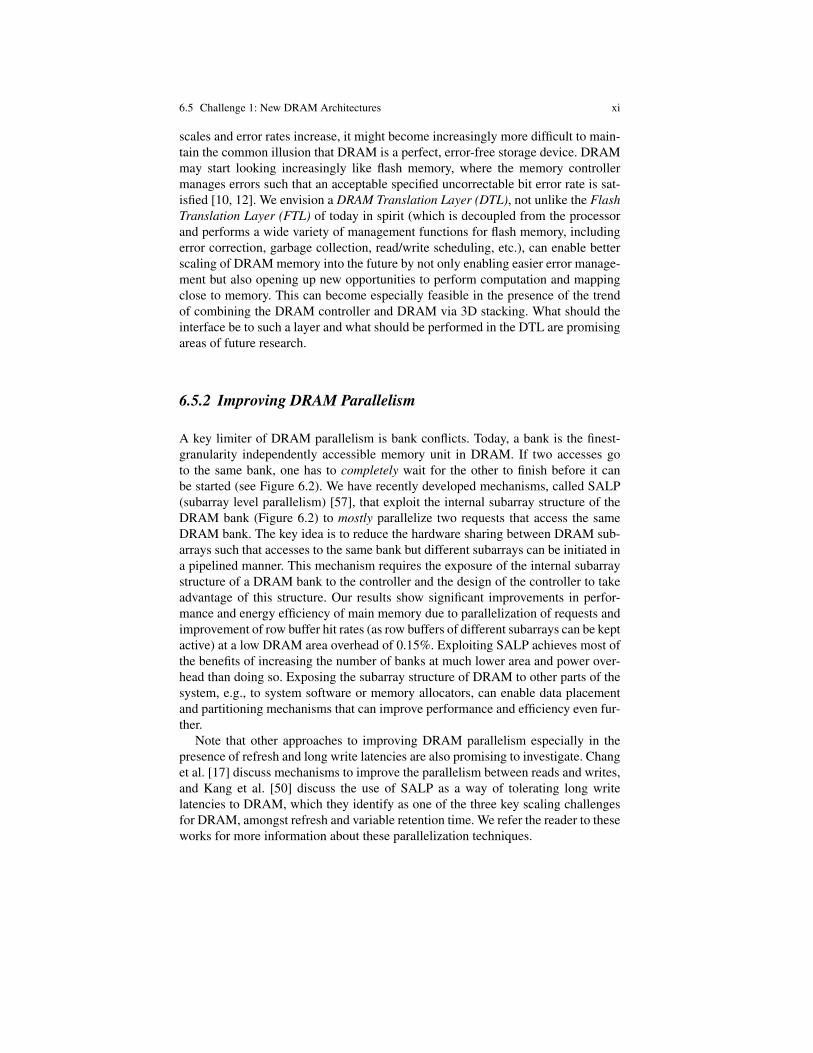
A key limiter of DRAM parallelism is bank conflicts. Today, a bank is the finest-granularity independently accessible memory unit in DRAM. If two accesses goto the same bank, one has to completely wait for the other to finish before it canbe started (see Figure 6.2). We have recently developed mechanisms, called SALP(subarray level parallelism) [57], that exploit the internal subarray structure of theDRAM bank (Figure 6.2) to mostly parallelize two requests that access the sameDRAM bank. The key idea is to reduce the hardware sharing between DRAM sub-arrays such that accesses to the same bank but different subarrays can be initiated ina pipelined manner. This mechanism requires the exposure of the internal subarraystructure of a DRAM bank to the controller and the design of the controller to takeadvantage of this structure. Our results show significant improvements in perfor-mance and energy efficiency of main memory due to parallelization of requests andimprovement of row buffer hit rates (as row buffers of different subarrays can be keptactive) at a low DRAM area overhead of 0.15%. Exploiting SALP achieves most ofthe benefits of increasing the number of banks at much lower area and power over-head than doing so. Exposing the subarray structure of DRAM to other parts of thesystem, e.g., to system software or memory allocators, can enable data placementand partitioning mechanisms that can improve performance and efficiency even fur-ther.
Note that other approaches to improving DRAM parallelism especially in thepresence of refresh and long write latencies are also promising to investigate. Changet al. [17] discuss mechanisms to improve the parallelism between reads and writes,and Kang et al. [50] discuss the use of SALP as a way of tolerating long writelatencies to DRAM, which they identify as one of the three key scaling challengesfor DRAM, amongst refresh and variable retention time. We refer the reader to theseworks for more information about these parallelization techniques.
xii 6 Main Memory Scaling: Challenges and Solution Directions
row
Bank
row-decoder
row-buffer
32
k ro
ws
(a) Logical abstraction of a bank
local row-buffer
Subarray1
global row-buffer
local row-buffer
Subarray64
glo
ba
l d
eco
de
r
51
2
rows
51
2
rows
(b) Implementation of a DRAM bank
Fig. 6.2. DRAM Bank Organization. Reproduced from [57].
6.5.3 Reducing DRAM Latency and Energy
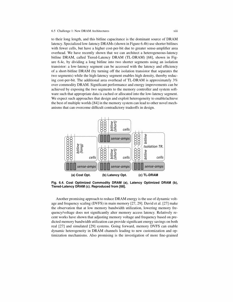
The DRAM industry has so far been primarily driven by the cost-per-bit metric:provide maximum capacity for a given cost. As shown in Figure 6.3, DRAM chipcapacity has increased by approximately 16X in 12 years while the DRAM latencyreduced by only approximately 20%. This is the result of a deliberate choice tomaximize capacity of a DRAM chip while minimizing its cost. We believe thischoice needs to be revisited in the presence of at least two key trends. First, DRAMlatency is becoming more important especially for response-time critical workloadsthat require QoS guarantees [28]. Second, DRAM capacity is becoming very hard toscale and as a result manufacturers likely need to provide new values for the DRAMchips, leading to more incentives for the production of DRAMs that are optimizedfor objectives other than mainly capacity maximization.
Fig. 6.3. DRAM Capacity & Latency Over Time. Reproduced from [68].
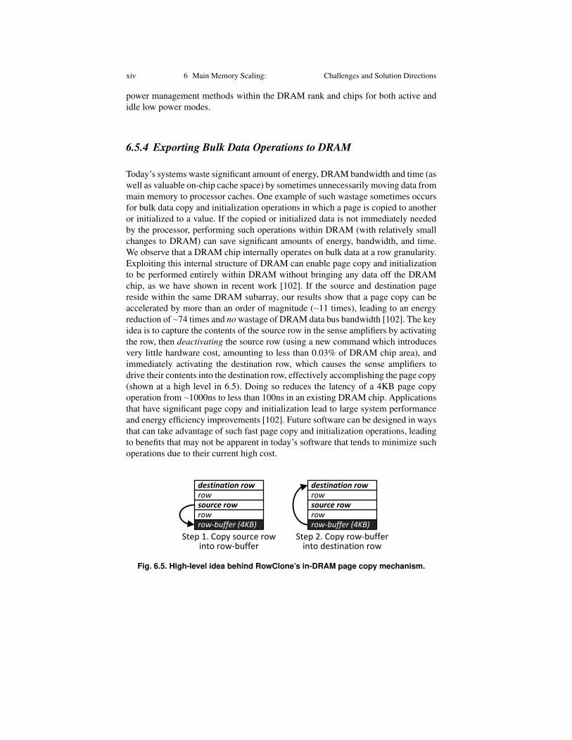
To mitigate the high area overhead of DRAM sensing structures, commodityDRAMs (shown in Figure 6.4a) connect many DRAM cells to each sense-amplifierthrough a wire called a bitline. These bitlines have a high parasitic capacitance due
6.5 Challenge 1: New DRAM Architectures xiii
to their long length, and this bitline capacitance is the dominant source of DRAMlatency. Specialized low-latency DRAMs (shown in Figure 6.4b) use shorter bitlineswith fewer cells, but have a higher cost-per-bit due to greater sense-amplifier areaoverhead. We have recently shown that we can architect a heterogeneous-latencybitline DRAM, called Tiered-Latency DRAM (TL-DRAM) [68], shown in Fig-ure 6.4c, by dividing a long bitline into two shorter segments using an isolationtransistor: a low-latency segment can be accessed with the latency and efficiencyof a short-bitline DRAM (by turning off the isolation transistor that separates thetwo segments) while the high-latency segment enables high density, thereby reduc-ing cost-per-bit. The additional area overhead of TL-DRAM is approximately 3%over commodity DRAM. Significant performance and energy improvements can beachieved by exposing the two segments to the memory controller and system soft-ware such that appropriate data is cached or allocated into the low-latency segment.We expect such approaches that design and exploit heterogeneity to enable/achievethe best of multiple worlds [84] in the memory system can lead to other novel mech-anisms that can overcome difficult contradictory tradeoffs in design.
sense-amps
cells
bitline
(long)
(a) Cost Opt.
sense-amps
cells
sense-amps
cells
bitline
(short)
bitline
(short)
(b) Latency Opt.
sense-amps
cellsbit
line
Isolation TR.b
itlin
e
(c) TL-DRAM
Fig. 6.4. Cost Optimized Commodity DRAM (a), Latency Optimized DRAM (b),Tiered-Latency DRAM (c). Reproduced from [68].
Another promising approach to reduce DRAM energy is the use of dynamic volt-age and frequency scaling (DVFS) in main memory [27, 29]. David et al. [27] makethe observation that at low memory bandwidth utilization, lowering memory fre-quency/voltage does not significantly alter memory access latency. Relatively re-cent works have shown that adjusting memory voltage and frequency based on pre-dicted memory bandwidth utilization can provide significant energy savings on bothreal [27] and simulated [29] systems. Going forward, memory DVFS can enabledynamic heterogeneity in DRAM channels leading to new customization and op-timization mechanisms. Also promising is the investigation of more fine-grained
xiv 6 Main Memory Scaling: Challenges and Solution Directions
power management methods within the DRAM rank and chips for both active andidle low power modes.
6.5.4 Exporting Bulk Data Operations to DRAM
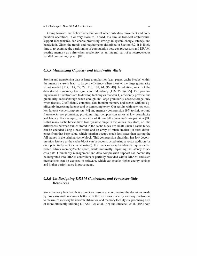
Today’s systems waste significant amount of energy, DRAM bandwidth and time (aswell as valuable on-chip cache space) by sometimes unnecessarily moving data frommain memory to processor caches. One example of such wastage sometimes occursfor bulk data copy and initialization operations in which a page is copied to anotheror initialized to a value. If the copied or initialized data is not immediately neededby the processor, performing such operations within DRAM (with relatively smallchanges to DRAM) can save significant amounts of energy, bandwidth, and time.We observe that a DRAM chip internally operates on bulk data at a row granularity.Exploiting this internal structure of DRAM can enable page copy and initializationto be performed entirely within DRAM without bringing any data off the DRAMchip, as we have shown in recent work [102]. If the source and destination pagereside within the same DRAM subarray, our results show that a page copy can beaccelerated by more than an order of magnitude (⇠11 times), leading to an energyreduction of ⇠74 times and no wastage of DRAM data bus bandwidth [102]. The keyidea is to capture the contents of the source row in the sense amplifiers by activatingthe row, then deactivating the source row (using a new command which introducesvery little hardware cost, amounting to less than 0.03% of DRAM chip area), andimmediately activating the destination row, which causes the sense amplifiers todrive their contents into the destination row, effectively accomplishing the page copy(shown at a high level in 6.5). Doing so reduces the latency of a 4KB page copyoperation from ⇠1000ns to less than 100ns in an existing DRAM chip. Applicationsthat have significant page copy and initialization lead to large system performanceand energy efficiency improvements [102]. Future software can be designed in waysthat can take advantage of such fast page copy and initialization operations, leadingto benefits that may not be apparent in today’s software that tends to minimize suchoperations due to their current high cost.
pro
cess
or
cache
core
memory controller DRAM
64B
64B
row-buffer (4Kbit)row (4Kbit)row (4Kbit)row (4Kbit)row (4Kbit)
2Gb DRAM Chip
row-buffer (4KB)
source row
destination row
row
row
row-buffer (4KB)
source row
destination row
row
row
Step 1. Copy source row into row-buffer
Step 2. Copy row-buffer into destination row
51
2ro
ws
Fig. 6.5. High-level idea behind RowClone’s in-DRAM page copy mechanism.
6.5 Challenge 1: New DRAM Architectures xv
Going forward, we believe acceleration of other bulk data movement and com-putation operations in or very close to DRAM, via similar low-cost architecturalsupport mechanisms, can enable promising savings in system energy, latency, andbandwidth. Given the trends and requirements described in Section 6.2, it is likelytime to re-examine the partitioning of computation between processors and DRAM,treating memory as a first-class accelerator as an integral part of a heterogeneousparallel computing system [84].
6.5.5 Minimizing Capacity and Bandwidth Waste
Storing and transferring data at large granularities (e.g., pages, cache blocks) withinthe memory system leads to large inefficiency when most of the large granularityis not needed [117, 118, 79, 78, 110, 101, 61, 96, 49]. In addition, much of thedata stored in memory has significant redundancy [116, 35, 94, 95]. Two promis-ing research directions are to develop techniques that can 1) efficiently provide finegranularity access/storage when enough and large granularity access/storage onlywhen needed, 2) efficiently compress data in main memory and caches without sig-nificantly increasing latency and system complexity. Our results with new low-cost,low-latency cache compression [94] and memory compression [95] techniques andframeworks are promising, providing high compression ratios at low complexityand latency. For example, the key idea of Base-Delta-Immediate compression [94]is that many cache blocks have low dynamic range in the values they store, i.e., thedifferences between values stored in the cache block are small. Such a cache blockcan be encoded using a base value and an array of much smaller (in size) differ-ences from that base value, which together occupy much less space than storing thefull values in the original cache block. This compression algorithm has low decom-pression latency as the cache block can be reconstructed using a vector addition (oreven potentially vector concatenation). It reduces memory bandwidth requirements,better utilizes memory/cache space, while minimally impacting the latency to ac-cess data. Granularity management and data compression support can potentiallybe integrated into DRAM controllers or partially provided within DRAM, and suchmechanisms can be exposed to software, which can enable higher energy savingsand higher performance improvements.
6.5.6 Co-Designing DRAM Controllers and Processor-SideResources
Since memory bandwidth is a precious resource, coordinating the decisions madeby processor-side resources better with the decisions made by memory controllersto maximize memory bandwidth utilization and memory locality is a promising areaof more efficiently utilizing DRAM. Lee et al. [67] and Stuecheli et al. [105] both
xvi 6 Main Memory Scaling: Challenges and Solution Directions
show that orchestrating last-level cache writebacks such that dirty cache lines tothe same row are evicted together from the cache improves DRAM row buffer lo-cality of write accesses, thereby improving system performance. Going forward,we believe such coordinated techniques between the processor-side resources andmemory controllers will become increasingly more effective as DRAM bandwidthbecomes even more precious. Mechanisms that predict and convey slack in memoryrequests [25], that orchestrate the on-chip scheduling of memory requests to im-prove memory bank parallelism [65] and that reorganize cache metadata for moreefficient bulk (DRAM row granularity) tag lookups [103] can also enable more effi-cient memory bandwidth utilization.
6.6 Challenge 2: Emerging Memory Technologies
While DRAM technology scaling is in jeopardy, some emerging technologies seemmore scalable. These include PCM and STT-MRAM. These emerging technologiesusually provide a tradeoff, and seem unlikely to completely replace DRAM (evalu-ated in [62, 63, 64] for PCM and in [60] for STT-MRAM), as they are not strictly su-perior to DRAM. For example, PCM is advantageous over DRAM because it 1) hasbeen demonstrated to scale to much smaller feature sizes and can store multiple bitsper cell [120], promising higher density, 2) is non-volatile and as such requires no re-fresh (which is a key scaling challenge of DRAM as we discussed in Section 6.5.1),and 3) has low idle power consumption. On the other hand, PCM has significantshortcomings compared to DRAM, which include 1) higher read latency and readenergy, 2) much higher write latency and write energy, and 3) limited endurance fora given PCM cell, a problem that does not exist (practically) for a DRAM cell. As aresult, an important research challenge is how to utilize such emerging technologiesat the system and architecture levels such that they can augment or perhaps evenreplace DRAM.
Our initial experiments and analyses [62, 63, 64] that evaluated the complete re-placement of DRAM with PCM showed that one would require reorganization of pe-ripheral circuitry of PCM chips (with the goal of absorbing writes and reads beforethey update or access the PCM cell array) to enable PCM to get close to DRAM per-formance and efficiency. These initial results are reported in Lee et al. [62, 63, 64].We have also reached a similar conclusion upon evaluation of the complete replace-ment of DRAM with STT-MRAM [60]: reorganization of peripheral circuitry ofSTT-MRAM chips (with the goal of minimizing the number of writes to the STT-MRAM cell array, as write operations are high-latency and high-energy in STT-MRAM) enables an STT-MRAM based main memory to be more energy-efficientthan a DRAM-based main memory.
One can achieve more efficient designs of PCM (or STT-MRAM) chips by tak-ing advantage of the non-destructive nature of reads, which enables simpler andnarrower row buffer organizations [78] Unlike in DRAM, the entire memory rowdoes not need to be buffered in a device where reading a memory row does not
6.6 Challenge 2: Emerging Memory Technologies xvii
destroy the data stored in the row. Meza et al. [78] show that having narrow rowbuffers in emerging non-volatile devices can greatly reduce main memory dynamicenergy compared to a DRAM baseline with large row sizes, without greatly affect-ing endurance, and for some NVM technologies, leading to improved performance.Going forward, designing systems, memory controllers and memory chips takingadvantage of the specific property of non-volatility of emerging technology seemspromising.
We believe emerging technologies enable at least three major system-level oppor-tunities that can improve overall system efficiency: 1) hybrid main memory systems,2) non-volatile main memory, 3) merging of memory and storage. We briefly touchupon each.
6.6.1 Hybrid Main Memory
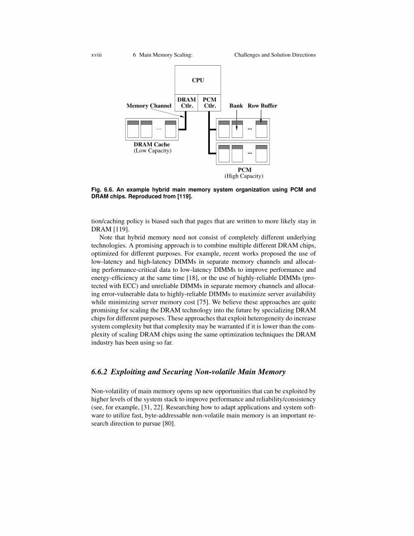
A hybrid main memory system [98, 30, 79, 119] consists of multiple different tech-nologies or multiple different types of the same technology with differing character-istics, e.g., performance, cost, energy, reliability, endurance. A key question is howto manage data allocation and movement between the different technologies suchthat one can achieve the best of (or close to the best of) the desired performancemetrics. In other words, we would like to exercise the advantages of each tech-nology as much as possible while hiding the disadvantages of any technology. Po-tential technologies include DRAM, 3D-stacked DRAM, embedded DRAM, PCM,STT-MRAM, other resistive memories, flash memory, forms of DRAM that are op-timized for different metrics and purposes, etc. An example hybrid main memorysystem consisting of a large amount of PCM as main memory and a small amountof DRAM as its cache is depicted in Figure 6.6.
The design space of hybrid memory systems is large, and many potential ques-tions exist. For example, should all memories be part of main memory or shouldsome of them be used as a cache of main memory (or should there be config-urability)? What technologies should be software visible? What component ofthe system should manage data allocation and movement? Should these tasks bedone in hardware, software, or collaboratively? At what granularity should datamoved between different memory technologies? Some of these questions are tack-led in [79, 119, 98, 30, 99], among other works recently published in the computerarchitecture community. For example, Yoon et al. [119] make the key observationthat row buffers are present in both DRAM and PCM, and they have (or can bedesigned to have) the same latency and bandwidth in both DRAM and PCM. Yet,row buffer misses are much more costly in terms of latency, bandwidth, and energyin PCM than in DRAM. To exploit this, we devise a policy that avoids accessingin PCM data that frequently causes row buffer misses. Hardware or software candynamically keep track of such data and allocate/cache it in DRAM while keep-ing data that frequently hits in row buffers in PCM. PCM also has much higherwrite latency/power than read latency/power: to take this into account, the alloca-
xviii 6 Main Memory Scaling: Challenges and Solution Directions
...
Ctlr. Ctlr.
...
...
DRAM PCM
(High Capacity)
(Low Capacity)
Row BufferBankMemory Channel
CPU
PCM
DRAM Cache
Fig. 6.6. An example hybrid main memory system organization using PCM andDRAM chips. Reproduced from [119].
tion/caching policy is biased such that pages that are written to more likely stay inDRAM [119].
Note that hybrid memory need not consist of completely different underlyingtechnologies. A promising approach is to combine multiple different DRAM chips,optimized for different purposes. For example, recent works proposed the use oflow-latency and high-latency DIMMs in separate memory channels and allocat-ing performance-critical data to low-latency DIMMs to improve performance andenergy-efficiency at the same time [18], or the use of highly-reliable DIMMs (pro-tected with ECC) and unreliable DIMMs in separate memory channels and allocat-ing error-vulnerable data to highly-reliable DIMMs to maximize server availabilitywhile minimizing server memory cost [75]. We believe these approaches are quitepromising for scaling the DRAM technology into the future by specializing DRAMchips for different purposes. These approaches that exploit heterogeneity do increasesystem complexity but that complexity may be warranted if it is lower than the com-plexity of scaling DRAM chips using the same optimization techniques the DRAMindustry has been using so far.
6.6.2 Exploiting and Securing Non-volatile Main Memory
Non-volatility of main memory opens up new opportunities that can be exploited byhigher levels of the system stack to improve performance and reliability/consistency(see, for example, [31, 22]. Researching how to adapt applications and system soft-ware to utilize fast, byte-addressable non-volatile main memory is an important re-search direction to pursue [80].
6.6 Challenge 2: Emerging Memory Technologies xix
On the flip side, the same non-volatility can lead to potentially unforeseen se-curity and privacy issues: critical and private data can persist long after the systemis powered down [20], and an attacker can take advantage of this fact. Wearout is-sues of emerging technology can also cause attacks that can intentionally degradememory capacity in the system [97, 104]. Securing non-volatile main memory istherefore an important systems challenge.
6.6.3 Merging of Memory and Storage
Traditional computer systems have a two-level storage model: they access and ma-nipulate 1) volatile data in main memory (DRAM, today) with a fast load/store inter-face, 2) persistent data in storage media (flash and hard disks, today) with a slowerfile system interface. Unfortunately, such a decoupled memory/storage model man-aged via vastly different techniques (fast, hardware-accelerated memory manage-ment units on one hand, and slow operating/file system (OS/FS) software on theother) suffers from large inefficiencies in locating data, moving data, and translatingdata between the different formats of these two levels of storage that are accessed viatwo vastly different interfacesleading to potentially large amounts of wasted workand energy [80]. The two different interfaces arose largely due to the large discrep-ancy in the access latencies of conventional technologies used to construct volatilememory (DRAM) and persistent storage (hard disks and flash memory).
Today, new non-volatile memory technologies (NVM), e.g, PCM, STT-MRAM,RRAM, show the promise of storage capacity and endurance similar to or better thanflash memory at latencies comparable to DRAM. This makes them prime candidatesfor providing applications a persistent single-level store with a single load/store-likeinterface to access all system data (including volatile and persistent data). In fact,if we keep the traditional two-level memory/storage model in the presence of thesefast NVM devices as part of storage, the operating system and file system code forlocating, moving, and translating persistent data from the non-volatile NVM devicesto volatile DRAM for manipulation purposes becomes a great bottleneck, causingmost of the memory energy consumption and degrading performance by an orderof magnitude in some data-intensive workloads, as we showed in recent work [80].With energy as a key constraint, and in light of modern high-density NVM devices, apromising research direction is to unify and coordinate the management of volatilememory and persistent storage in a single level, to eliminate wasted energy andperformance, and to simplify the programming model at the same time.
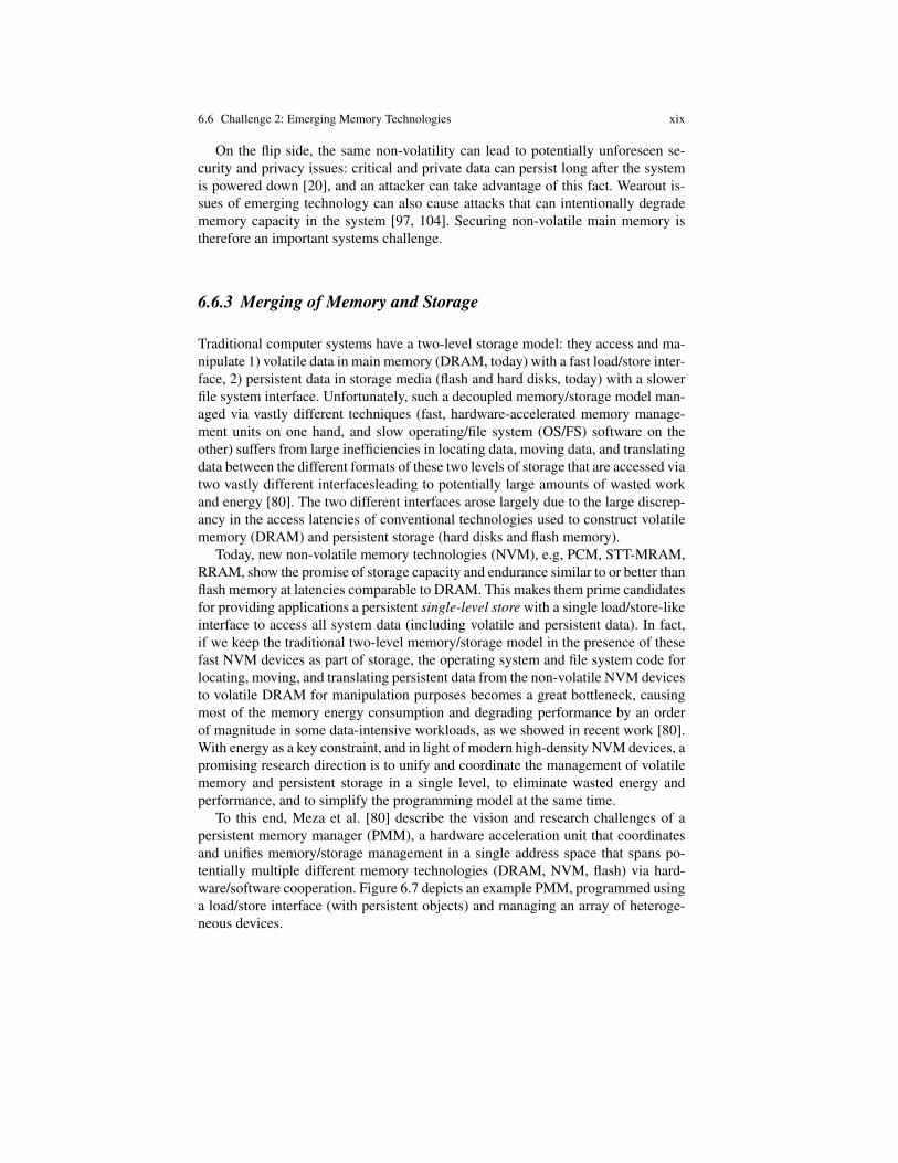
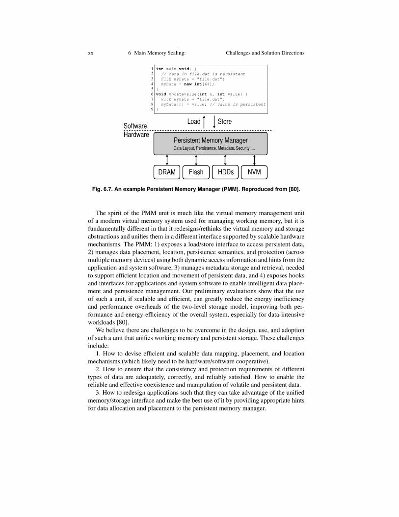
To this end, Meza et al. [80] describe the vision and research challenges of apersistent memory manager (PMM), a hardware acceleration unit that coordinatesand unifies memory/storage management in a single address space that spans po-tentially multiple different memory technologies (DRAM, NVM, flash) via hard-ware/software cooperation. Figure 6.7 depicts an example PMM, programmed usinga load/store interface (with persistent objects) and managing an array of heteroge-neous devices.
xx 6 Main Memory Scaling: Challenges and Solution Directions
2.2.1 Efficient Hardware and Software Support: We propose to investigate the efficient software andhardware support needed for single-level stores. A single-level store system should provide an abstractionthat maps persistent user data to physical addresses in memory. A software interface for programs wouldmap a pointer to the actual persistent data. Programs would be able to access any part of the data usingnormal load and store instructions. Figure 2 shows two examples of high-level abstractions which couldbe provided to programs to access persistent data in a single-level store system. In it, a program createsa persistent file (Figure 2 left) or object (Figure 2 right) using the handle “file.dat” and allocates an arrayof integers in it. Later—perhaps after the application or system is restarted—when the program executesthe updateValue() function, the system retrieves the persistent data for the same handle, and the programmodifies its state. With such an abstraction, a single-level store can eliminate the OS system calls to transferdata to and from disk. In addition, it eliminates the need for a file system to track physical file addressesby traversing metadata (such as inodes) in the OS. In this way, single-level stores provide the opportunity todesign a simple and efficient persistent data lookup system in hardware. We plan to research efficient waysto map files or objects to the virtual address space. In such a hardware-based design, the processor wouldmanage how data handles correspond to physical addresses. Note that, single-level stores can use alternativedesign choices, such as segments, to provide the high-level abstraction instead of files or objects. Regardless,segments, files, or objects will be mapped to physical addresses with hardware support. Prior works tried tomake file lookup and update efficient in software [27, 28] in the presence of persistent memory, and otherworks proposed using complex and potentially inefficient hardware directory techniques (e.g., [15]). Ourgoal is to design fast and efficient techniques that take into account the byte addressability of persistentmemory in a single-level store. To this end, we will research the following:• The efficient use of hash table and B-tree indices for locating files in a single-level store.• How techniques such as key-value stores can provide fast and efficient lookups in single-level stores.• Policies for intelligently caching some entries of these indices in hardware to improve system perfor-
mance.Every access in the single-level store needs to be translated from a virtual address used by a program to
a physical address used to access a device. We will investigate how to efficiently manage address translationso that locating data is simple and fast. We intend to explore the following directions to solve this problem:• We will design mechanisms to predict access patterns based on program behavior and pre-compute
virtual-to-physical address translations. We are interested in answering questions such as: What is thepattern of data accesses to a single-level store, and how can prefetching techniques be redesigned withsingle-level stores in mind to enable efficient address translation? How can simple application-level orprofile-based hints on access patterns be communicated to and used by hardware to make address translationand prefetching efficient?• We will design efficient translation lookaside buffer (TLB)-like structures which will cache the trans-
lation between virtual and physical addresses but for a much larger amount of physical memory than inexisting systems. In the presence of such a single-level store, many disparate data accesses could need alarge translation table to be serviced effectively. To reduce overhead of such hardware, we are interested inexploring whether TLB-like structures should favor storing translations only for particular classes of data,such as data with locality or data which is on the critical path of execution, which get the most benefitout of the limited structure space. In addition, we will investigate centralized versus distributed translationstructures to design techniques that, for example, buffer private data translation entries near the processor,while distributing shared entries across processors to minimize translation overheads. Such translation struc-
1 int main(void) {2 // data in file.dat is persistent3 FILE myData = "file.dat";4 myData = new int[64];5 }6 void updateValue(int n, int value) {7 FILE myData = "file.dat";8 myData[n] = value; // value is persistent9 }
1 int main(void) {2 // data in file.dat is persistent3 int *myData = new PersistentObject("file.dat");4 myData = new int[64];5 }6 void updateValue(int n, int value) {7 int *myData = PersistentObject.open("file.dat");8 myData[n] = value; // value is persistent9 }
Figure 2: Sample program with access to file-based (left) and object-based (right) persistent data.
5
Load Store
DRAM Flash HDDs NVM
Persistent Memory ManagerHardwareSoftware
Data Layout, Persistence, Metadata, Security, ...
Fig. 6.7. An example Persistent Memory Manager (PMM). Reproduced from [80].
The spirit of the PMM unit is much like the virtual memory management unitof a modern virtual memory system used for managing working memory, but it isfundamentally different in that it redesigns/rethinks the virtual memory and storageabstractions and unifies them in a different interface supported by scalable hardwaremechanisms. The PMM: 1) exposes a load/store interface to access persistent data,2) manages data placement, location, persistence semantics, and protection (acrossmultiple memory devices) using both dynamic access information and hints from theapplication and system software, 3) manages metadata storage and retrieval, neededto support efficient location and movement of persistent data, and 4) exposes hooksand interfaces for applications and system software to enable intelligent data place-ment and persistence management. Our preliminary evaluations show that the useof such a unit, if scalable and efficient, can greatly reduce the energy inefficiencyand performance overheads of the two-level storage model, improving both per-formance and energy-efficiency of the overall system, especially for data-intensiveworkloads [80].
We believe there are challenges to be overcome in the design, use, and adoptionof such a unit that unifies working memory and persistent storage. These challengesinclude:
1. How to devise efficient and scalable data mapping, placement, and locationmechanisms (which likely need to be hardware/software cooperative).
2. How to ensure that the consistency and protection requirements of differenttypes of data are adequately, correctly, and reliably satisfied. How to enable thereliable and effective coexistence and manipulation of volatile and persistent data.
3. How to redesign applications such that they can take advantage of the unifiedmemory/storage interface and make the best use of it by providing appropriate hintsfor data allocation and placement to the persistent memory manager.
6.7 Challenge 3: Predictable Performance xxi
4. How to provide efficient and high-performance backward compatibility mech-anisms for enabling and enhancing existing memory and storage interfaces in asingle-level store. These techniques can seamlessly enable applications targeting tra-ditional two-level storage systems to take advantage of the performance and energy-efficiency benefits of systems employing single-level stores. We believe such tech-niques are needed to ease the software transition to a radically different storageinterface.
6.7 Challenge 3: Predictable Performance
Since memory is a shared resource between multiple cores (or, agents, threads,or applications and virtual machines), different applications contend for memorybandwidth and capacity. As such, memory contention, or memory interference, be-tween different cores critically affects both the overall system performance and eachapplication’s performance. Providing the appropriate bandwidth and capacity al-location to each application such that its performance requirements are satisfiedis important to satisfy user expectations and service level agreements, and at thesame time enable better system performance. Our past work (e.g., [81, 87, 88])showed that application-unaware design of memory controllers, and in particularmemory scheduling algorithms, leads to uncontrolled interference of applications inthe memory system. Such uncontrolled interference can lead to denial of service tosome applications [81], low system performance [87, 88], and an inability to satisfyperformance requirements [87, 106, 32], which makes the system uncontrollableand unpredictable. In fact, an application’s performance depends on what other ap-plications it is sharing resources with: an application can sometimes have very highperformance and at other times very low performance on the same system, solelydepending on its co-runners. A critical research challenge is therefore how to designthe memory system (including all shared resources such as main memory, caches,and interconnects) such that 1) the performance of each application is predictableand controllable, 2) while the performance and efficiency of the entire system are ashigh as needed or possible.
To achieve these goals, we have designed various solutions including QoS-aware memory controllers [87, 88, 82, 55, 56, 83, 6, 106, 66, 33], intercon-nects [24, 25, 38, 39, 16, 91, 92, 26], and entire memory systems including caches,interconnect, and memory [32, 34, 26]. These works enhanced our understandingof memory interference in multi-core and heterogeneous systems and provide vi-able and effective mechanisms that improve overall system performance, while alsoproviding a fairness substrate that can enable fair memory service, which can beconfigured to enforce different application priorities.
A promising direction going forward is to devise mechanisms that are effectiveand accurate at 1) estimating and predicting application performance in the presenceof interference and a dynamic system with continuously incoming and outgoing ap-plications and 2) enforcing end-to-end performance guarantees within the entire
xxii 6 Main Memory Scaling: Challenges and Solution Directions
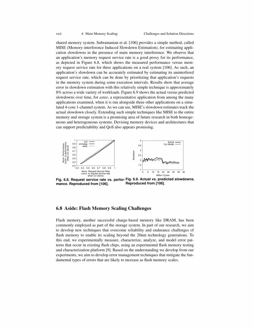
shared memory system. Subramanian et al. [106] provides a simple method, calledMISE (Memory-interference Induced Slowdown Estimation), for estimating appli-cation slowdowns in the presence of main memory interference. We observe thatan application’s memory request service rate is a good proxy for its performance,as depicted in Figure 6.8, which shows the measured performance versus mem-ory request service rate for three applications on a real system [106]. As such, anapplication’s slowdown can be accurately estimated by estimating its uninterferedrequest service rate, which can be done by prioritizing that application’s requestsin the memory system during some execution intervals. Results show that averageerror in slowdown estimation with this relatively simple technique is approximately8% across a wide variety of workloads. Figure 6.9 shows the actual versus predictedslowdowns over time, for astar, a representative application from among the manyapplications examined, when it is run alongside three other applications on a simu-lated 4-core 1-channel system. As we can see, MISE’s slowdown estimates track theactual slowdown closely. Extending such simple techniques like MISE to the entirememory and storage system is a promising area of future research in both homoge-neous and heterogeneous systems. Devising memory devices and architectures thatcan support predictability and QoS also appears promising.
0.3
0.4
0.5
0.6
0.7
0.8
0.9
1
0.3 0.4 0.5 0.6 0.7 0.8 0.9 1
Norm
. P
erf
orm
ance
(norm
. to
perf
orm
ance
when r
un a
lone)
Norm. Request Service Rate(norm. to request service rate
when run alone)
mcfomnetpp
astar
Fig. 6.8. Request service rate vs. perfor-mance. Reproduced from [106].
1
1.5
2
2.5
3
3.5
4
0 5 10 15 20 25 30 35 40
Slo
wd
ow
n
Million Cycles
ActualOur Model
Fig. 6.9. Actual vs. predicted slowdowns.Reproduced from [106].
6.8 Aside: Flash Memory Scaling Challenges
Flash memory, another successful charge-based memory like DRAM, has beencommonly employed as part of the storage system. In part of our research, we aimto develop new techniques that overcome reliability and endurance challenges offlash memory to enable its scaling beyond the 20nm technology generations. Tothis end, we experimentally measure, characterize, analyze, and model error pat-terns that occur in existing flash chips, using an experimental flash memory testingand characterization platform [9]. Based on the understanding we develop from ourexperiments, we aim to develop error management techniques that mitigate the fun-damental types of errors that are likely to increase as flash memory scales.
6.8 Aside: Flash Memory Scaling Challenges xxiii
We have recently experimentally characterized complex flash errors that occurat 30-40nm flash technologies [10], categorizing them into four types: retention er-rors, program interference errors, read errors, and erase errors. Our characterizationshows the relationship between various types of errors and demonstrates empiricallyusing real 3x-nm flash chips that retention errors are the most dominant error type.Our results demonstrate that different flash errors have distinct patterns: retentionerrors and program interference errors are program/erase-(P/E)-cycle-dependent,memory-location-dependent, and data-value-dependent. Since the observed errorpatterns are due to fundamental circuit and device behavior inherent in flash mem-ory, we expect our observations and error patterns to also hold in flash memoriesbeyond 30-nm technology.
Based on our experimental characterization results that show that the retentionerrors are the most dominant errors, we have developed a suite of techniques tomitigate the effects of such errors, called Flash Correct-and-Refresh (FCR) [11]. Thekey idea is to periodically read each page in flash memory, correct its errors usingsimple error correcting codes (ECC), and either remap (copy/move) the page to adifferent location or reprogram it in its original location by recharging the floatinggates, before the page accumulates more errors than can be corrected with simpleECC. Our simulation experiments using real I/O workload traces from a variety offile system, database, and search applications show that FCR can provide 46x flashmemory lifetime improvement at only 1.5% energy overhead, with no additionalhardware cost.
Recently, we have also experimentally investigated and characterized the thresh-old voltage distribution of different logical states in MLC NAND flash memory [14].We have developed new models that can predict the shifts in the threshold voltagedistribution based on the number of P/E cycles endured by flash memory cells. Ourdata shows that the threshold voltage distribution of flash cells that store the samevalue can be approximated, with reasonable accuracy, as a Gaussian distribution.The threshold voltage distribution of flash cells that store the same value gets dis-torted as the number of P/E cycles increases, causing threshold voltages of cellsstoring different values to overlap with each other, which can lead to the incorrectreading of values of some cells as flash cells accumulate P/E cycles. We find thatthis distortion can be accurately modeled and predicted as an exponential functionof the P/E cycles, with more than 95% accuracy. Such predictive models can aid thedesign of more sophisticated error correction methods, such as LDPC codes [37],which are likely needed for reliable operation of future flash memories.
We are currently investigating another increasingly significant obstacle to MLCNAND flash scaling, which is the increasing cell-to-cell program interference due toincreasing parasitic capacitances between the cells’ floating gates. Accurate charac-terization and modeling of this phenomenon are needed to find effective techniquesto combat program interference. In recent work [13], we leverage the read retrymechanism found in some flash designs to obtain measured threshold voltage distri-butions from state-of-the-art 2Y-nm (i.e., 24-20 nm) MLC NAND flash chips. Theseresults are then used to characterize the cell-to-cell program interference under var-ious programming conditions. We show that program interference can be accurately
xxiv 6 Main Memory Scaling: Challenges and Solution Directions
modeled as additive noise following Gaussian-mixture distributions, which can bepredicted with 96.8% accuracy using linear regression models. We use these modelsto develop and evaluate a read reference voltage prediction technique that reducesthe raw flash bit error rate by 64% and increases the flash lifetime by 30%. Moredetail can be found in Cai et al. [13].
Most recently, to improve flash memory lifetime, we have developed a mecha-nism called Neighbor-Cell Assisted Correction (NAC) [15], which uses the valueinformation of cells in a neighboring page to correct errors found on a page whenreading. This mechanism takes advantage of the new empirical observation thatidentifying the value stored in the immediate-neighbor cell makes it easier to de-termine the data value stored in the cell that is being read. The key idea is to re-reada flash memory page that fails error correction codes (ECC) with the set of readreference voltage values corresponding to the conditional threshold voltage distri-bution assuming a neighbor cell value and use the re-read values to correct the cellsthat have neighbors with that value. Our simulations show that NAC effectively im-proves flash memory lifetime by 33% while having no (at nominal lifetime) or verymodest (less than 5% at extended lifetime) performance overhead.
Going forward, we believe more accurate and detailed characterization of flashmemory error mechanisms are needed to devise models that can aid the design ofmore efficient and effective mechanisms to tolerate errors found in sub-20nm flashmemories. A promising direction is the design of predictive models that the system(e.g., the flash controller or system software) can use to proactively estimate theoccurrence of errors and take action to prevent the error before it happens. Flash-correct-and-refresh [11], read reference voltage prediction [13], described earlier,are early forms of such predictive error tolerance mechanisms.
6.9 Conclusion
We have described several research directions and ideas to enhance memory scalingvia system and architecture-level approaches. A promising approach is the co-designof memory and other system components to enable better system optimization. En-abling better cooperation across multiple levels of the computing stack, includingsoftware, microarchitecture, and devices can help scale the memory system by ex-posing more of the memory device characteristics to higher levels of the systemstack such that the latter can tolerate and exploit such characteristics. Finally, het-erogeneity in the design of the memory system can help overcome the memoryscaling challenges at the device level by enabling better specialization of the mem-ory system and its dynamic adaptation to different demands of various applications.We believe such approaches will become increasingly important and effective as theunderlying memory technology nears its scaling limits at the physical level and en-vision a near future full of innovation in main memory architecture, enabled by theco-design of the system and main memory.
References xxv
Acknowledgments
I would like to thank my PhD students Rachata Ausavarungnirun and LavanyaSubramanian for logistic help in preparing this chapter and earlier versions of it.Many thanks to all my students in my SAFARI research group and collaborators atCarnegie Mellon as well as other universities, whom all contributed to the worksoutlined in this chapter. Thanks also go to my research group’s industrial sponsorsover the past six years, including AMD, HP Labs, IBM, Intel, Microsoft, Nvidia,Oracle, Qualcomm, Samsung. Some of the research reported here was also par-tially supported by GSRC, Intel URO Memory Hierarchy Program, Intel Scienceand Technology Center on Cloud Computing, NIH, NSF, and SRC.
This chapter is a significantly extended and revised version of an invited pa-per that appeared at the 5th International Memory Workshop [85], which was alsopresented at MemCon 2013 [86]. Part of the structure of this chapter is based onan evolving set of talks I have delivered at various venues on Scaling the MemorySystem in the Many-Core Era and Rethinking Memory System Design for Data-Intensive Computing between 2010-2014, including invited talks at the 2011 In-ternational Symposium on Memory Management and ACM SIGPLAN Workshopon Memory System Performance and Correctness [89] and the 2012 DAC MoreThan Moore Technologies Workshop. Section 6.8 of this article is a condensed andslightly revised version of the introduction of an invited article that appeared in aspecial issue of the Intel Technology Journal, titled Error Analysis and Retention-Aware Error Management for NAND Flash Memory [12].
References
1. International technology roadmap for semiconductors (ITRS) (2011)2. Hybrid Memory Consortium (2012). http://www.hybridmemorycube.org3. Ahn, J.H., et al.: Adaptive self refresh scheme for battery operated high-density mobile dram
applications. In: ASSCC (2006)4. Alkan, C., et al.: Personalized copy-number and segmental duplication maps using next-
generation sequencing. In: Nature Genetics (2009)5. Atwood, G.: Current and emerging memory technology landscape. In: Flash Memory Sum-
mit (2011)6. Ausavarungnirun, R., et al.: Staged memory scheduling: Achieving high performance and
scalability in heterogeneous systems. In: ISCA (2012)7. Bloom, B.H.: Space/time trade-offs in hash coding with allowable errors. Communications
of the ACM 13(7), 422–426 (1970)8. Bryant, R.: Data-intensive supercomputing: The case for DISC. CMU CS Tech. Report 07-
128 (2007)9. Cai, Y., et al.: FPGA-based solid-state drive prototyping platform. In: FCCM (2011)
10. Cai, Y., et al.: Error patterns in MLC NAND flash memory: Measurement, characterization,and analysis. In: DATE (2012)
11. Cai, Y., et al.: Flash Correct-and-Refresh: Retention-aware error management for increasedflash memory lifetime. In: ICCD (2012)
12. Cai, Y., et al.: Error analysis and retention-aware error management for nand flash memory.Intel technology Journal 17(1) (2013)
xxvi 6 Main Memory Scaling: Challenges and Solution Directions
13. Cai, Y., et al.: Program interference in MLC NAND flash memory: Characterization, model-ing, and mitigation. In: ICCD (2013)
14. Cai, Y., et al.: Threshold voltage distribution in MLC NAND flash memory: Characterization,analysis and modeling. In: DATE (2013)
15. Cai, Y., et al.: Neighbor-cell assisted error correction for MLC NAND flash memories. In:SIGMETRICS (2014)
16. Chang, K., et al.: HAT: Heterogeneous adaptive throttling for on-chip networks. In: SBAC-PAD (2012)
17. Chang, K., et al.: Improving DRAM performance by parallelizing refreshes with accesses.In: HPCA (2014)
18. Chatterjee, N., et al.: Leveraging heterogeneity in DRAM main memories to accelerate crit-ical word access. In: MICRO (2012)
19. Chen, E., et al.: Advances and future prospects of spin-transfer torque random access mem-ory. IEEE Transactions on Magnetics 46(6) (2010)
20. Chhabra, S., Solihin, Y.: i-nvmm: a secure non-volatile main memory system with incremen-tal encryption. In: ISCA (2011)
21. Chung, E., et al.: Single-chip heterogeneous computing: Does the future include customlogic, FPGAs, and GPUs? In: MICRO (2010)
22. Condit, J., et al.: Better I/O through byte-addressable, persistent memory. In: SOSP (2009)23. Craeynest, K.V., et al.: Scheduling heterogeneous multi-cores through performance impact
estimation (PIE). In: ISCA (2012)24. Das, R., et al.: Application-aware prioritization mechanisms for on-chip networks. In: MI-
CRO (2009)25. Das, R., et al.: Aergia: Exploiting packet latency slack in on-chip networks. In: ISCA (2010)26. Das, R., et al.: Application-to-core mapping policies to reduce memory system interference
in multi-core systems. In: HPCA (2013)27. David, H., et al.: Memory power management via dynamic voltage/frequency scaling. In:
ICAC (2011)28. Dean, J., Barroso, L.A.: The tail at scale. Communications of the ACM 56(2), 74–80 (2013)29. Deng, Q., et al.: MemScale: active low-power modes for main memory. In: ASPLOS (2011)30. Dhiman, G.: PDRAM: A hybrid PRAM and DRAM main memory system. In: DAC (2009)31. Dong, X., et al.: Leveraging 3D PCRAM technologies to reduce checkpoint overhead for
future exascale systems. In: SC (2009)32. Ebrahimi, E., et al.: Fairness via source throttling: a configurable and high-performance fair-
ness substrate for multi-core memory systems. In: ASPLOS (2010)33. Ebrahimi, E., et al.: Parallel application memory scheduling. In: MICRO (2011)34. Ebrahimi, E., et al.: Prefetch-aware shared-resource management for multi-core systems. In:
ISCA (2011)35. Ekman, M.: A robust main-memory compression scheme. In: ISCA (2005)36. Eyerman, S., Eeckhout, L.: Modeling critical sections in amdahl’s law and its implications
for multicore design. In: ISCA (2010)37. Gallager, R.: Low density parity check codes (1963). MIT Press38. Grot, B., et al.: Preemptive virtual clock: A flexible, efcient, and cost-effective qos scheme
for networks-on-chip. In: MICRO (2009)39. Grot, B., et al.: Kilo-NOC: A heterogeneous network-on-chip architecture for scalability and
service guarantees. In: ISCA (2011)40. Hong, S.: Memory technology trend and future challenges. In: IEDM (2010)41. Ipek, E., Mutlu, O., Martinez, J.F., Caruana, R.: Self-optimizing memory controllers: A re-
inforcement learning approach. In: ISCA (2008)42. Isen, C., John, L.K.: Eskimo: Energy savings using semantic knowledge of inconsequential
memory occupancy for dram subsystem. In: MICRO (2009)43. Iyer, R.: CQoS: a framework for enabling QoS in shared caches of CMP platforms. In: ICS
(2004)44. Iyer, R., et al.: QoS policies and architecture for cache/memory in cmp platforms. In: SIG-
METRICS (2007)
References xxvii
45. Joao, J.A., et al.: Bottleneck identification and scheduling in multithreaded applications. In:ASPLOS (2012)
46. Joao, J.A., et al.: Utility-based acceleration of multithreaded applications on asymmetriccmps. In: ISCA (2013)
47. Jog, A., et al.: Orchestrated scheduling and prefetching for GPGPUs. In: ISCA (2013)48. Jog, A., et al.: OWL: Cooperative thread array aware scheduling techniques for improving
GPGPU performance. In: ASPLOS (2013)49. Johnson, T.L., et al.: Run-time spatial locality detection and optimization. In: MICRO (1997)50. Kang, U., et al.: Co-architecting controllers and DRAM to enhance DRAM process scaling.
In: The Memory Forum (2014)51. Khan, S., et al.: The efficacy of error mitigation techniques for DRAM retention failures: A
comparative experimental study. In: SIGMETRICS (2014)52. Kim, J., Papaefthymiou, M.C.: Dynamic memory design for low data-retention power. In:
PATMOS (2000)53. Kim, K.: Future memory technology: challenges and opportunities. In: VLSI-TSA (2008)54. Kim, K., et al.: A new investigation of data retention time in truly nanoscaled DRAMs. IEEE
Electron Device Letters 30(8) (2009)55. Kim, Y., et al.: ATLAS: a scalable and high-performance scheduling algorithm for multiple
memory controllers. In: HPCA (2010)56. Kim, Y., et al.: Thread cluster memory scheduling: Exploiting differences in memory access
behavior. In: MICRO (2010)57. Kim, Y., et al.: A case for subarray-level parallelism (SALP) in DRAM. In: ISCA (2012)58. Kim, Y., et al.: Flipping bits in memory without accessing them: An experimental study of
DRAM disturbance errors. In: ISCA (2014)59. Koh, Y.: NAND Flash Scaling Beyond 20nm. In: IMW (2009)60. Kultursay, E., et al.: Evaluating STT-RAM as an energy-efficient main memory alternative.
In: ISPASS (2013)61. Kumar, S., Wilkerson, C.: Exploiting spatial locality in data caches using spatial footprints.
In: ISCA (1998)62. Lee, B.C., et al.: Architecting Phase Change Memory as a Scalable DRAM Alternative. In:
ISCA (2009)63. Lee, B.C., et al.: Phase change memory architecture and the quest for scalability. Communi-
cations of the ACM 53(7), 99–106 (2010)64. Lee, B.C., et al.: Phase change technology and the future of main memory. IEEE Micro (Top
Picks Issue) 30(1) (2010)65. Lee, C.J., Narasiman, V., Mutlu, O., Patt, Y.N.: Improving memory bank-level parallelism in
the presence of prefetching. In: MICRO (2009)66. Lee, C.J., et al.: Prefetch-aware DRAM controllers. In: MICRO (2008)67. Lee, C.J., et al.: DRAM-aware last-level cache writeback: Reducing write-caused interfer-
ence in memory systems. Tech. Rep. TR-HPS-2010-002, HPS (2010)68. Lee, D., et al.: Tiered-latency DRAM: A low latency and low cost DRAM architecture. In:
HPCA (2013)69. Lefurgy, C., et al.: Energy management for commercial servers. In: IEEE Computer (2003)70. Lim, K., et al.: Disaggregated memory for expansion and sharing in blade servers. In: ISCA
(2009)71. Liu, J., et al.: RAIDR: Retention-aware intelligent DRAM refresh. In: ISCA (2012)72. Liu, J., et al.: An experimental study of data retention behavior in modern DRAM devices:
Implications for retention time profiling mechanisms. In: ISCA (2013)73. Liu, S., et al.: Flikker: saving dram refresh-power through critical data partitioning. In:
ASPLOS (2011)74. Loh, G.: 3D-stacked memory architectures for multi-core processors. In: ISCA (2008)75. Luo, Y., et al.: Characterizing application memory error vulnerability to optimize data center
cost via heterogeneous-reliability memory. In: DSN (2014)76. Maislos, A., et al.: A new era in embedded flash memory. In: FMS (2011)
xxviii 6 Main Memory Scaling: Challenges and Solution Directions
77. Mandelman, J., et al.: Challenges and future directions for the scaling of dynamic random-access memory (DRAM). In: IBM JR&D (2002)
78. Meza, J., et al.: A case for small row buffers in non-volatile main memories. In: ICCD (2012)79. Meza, J., et al.: Enabling efficient and scalable hybrid memories using fine-granularity
DRAM cache management. IEEE CAL (2012)80. Meza, J., et al.: A case for efficient hardware-software cooperative management of storage
and memory. In: WEED (2013)81. Moscibroda, T., Mutlu, O.: Memory performance attacks: Denial of memory service in multi-
core systems. In: USENIX Security (2007)82. Moscibroda, T., Mutlu, O.: Distributed order scheduling and its application to multi-core
DRAM controllers. In: PODC (2008)83. Muralidhara, S., et al.: Reducing memory interference in multi-core systems via application-
aware memory channel partitioning. In: MICRO (2011)84. Mutlu, O.: Asymmetry everywhere (with automatic resource management). In: CRA Work-
shop on Adv. Comp. Arch. Research (2010)85. Mutlu, O.: Memory scaling: A systems architecture perspective. In: IMW (2013)86. Mutlu, O.: Memory scaling: A systems architecture perspective. In: MemCon (2013)87. Mutlu, O., Moscibroda, T.: Stall-time fair memory access scheduling for chip multiproces-
sors. In: MICRO (2007)88. Mutlu, O., Moscibroda, T.: Parallelism-aware batch scheduling: Enhancing both performance
and fairness of shared DRAM systems. In: ISCA (2008)89. Mutlu, O., et al.: Memory systems in the many-core era: Challenges, opportunities, and so-
lution directions. In: ISMM (2011). http://users.ece.cmu.edu/˜
omutlu/pub/
onur-ismm-mspc-keynote-june-5-2011-short.pptx
90. Nair, P.J., et al.: ArchShield: Architectural Framework for Assisting DRAM Scaling by Tol-erating High Error Rates. In: ISCA (2013)
91. Nychis, G., et al.: Next generation on-chip networks: What kind of congestion control do weneed? In: HotNets (2010)
92. Nychis, G., et al.: On-chip networks from a networking perspective: Congestion and scala-bility in many-core interconnects. In: SIGCOMM (2012)
93. Ohsawa, T., et al.: Optimizing the DRAM refresh count for merged DRAM/logic LSIs. In:ISLPED (1998)
94. Pekhimenko, G., et al.: Base-delta-immediate compression: A practical data compressionmechanism for on-chip caches. In: PACT (2012)
95. Pekhimenko, G., et al.: Linearly compressed pages: A main memory compression frameworkwith low complexity and low latency. MICRO (2013)
96. Qureshi, M.K., et al.: Line distillation: Increasing cache capacity by filtering unused wordsin cache lines. In: HPCA (2007)
97. Qureshi, M.K., et al.: Enhancing lifetime and security of phase change memories via start-gap wear leveling. In: MICRO (2009)
98. Qureshi, M.K., et al.: Scalable high performance main memory system using phase-changememory technology. In: ISCA (2009)
99. Ramos, L.E., et al.: Page placement in hybrid memory systems. In: ICS (2011)100. Raoux, S., et al.: Phase-change random access memory: A scalable technology. IBM JR&D
52 (2008)101. Seshadri, V., et al.: The evicted-address filter: A unified mechanism to address both cache
pollution and thrashing. In: PACT (2012)102. Seshadri, V., et al.: RowClone: Fast and efficient In-DRAM copy and initialization of bulk
data. MICRO (2013)103. Seshadri, V., et al.: The dirty-block index. In: ISCA (2014)104. Song, N.H., et al.: Security refresh: prevent malicious wear-out and increase durability for
phase-change memory with dynamically randomized address mapping. In: ISCA (2010)105. Stuecheli, J., et al.: The virtual write queue: Coordinating DRAM and last-level cache poli-
cies. In: ISCA-37 (2010)
106. Subramanian, L., et al.: MISE: Providing performance predictability and improving fairnessin shared main memory systems. In: HPCA (2013)
107. Suleman, M.A., et al.: Accelerating critical section execution with asymmetric multi-corearchitectures. In: ASPLOS (2009)
108. Tang, L., et al.: The impact of memory subsystem resource sharing on datacenter applica-tions. In: ISCA (2011)
109. Treangen, T., Salzberg, S.: Repetitive DNA and next-generation sequencing: computationalchallenges and solutions. In: Nature Reviews Genetics (2012)
110. Udipi, A., et al.: Rethinking DRAM design and organization for energy-constrained multi-cores. In: ISCA (2010)
111. Udipi, A., et al.: Combining memory and a controller with photonics through 3d-stacking toenable scalable and energy-efficient systems. In: ISCA (2011)
112. Venkatesan, R.K., et al.: Retention-aware placement in DRAM (RAPID): Software methodsfor quasi-non-volatile DRAM. In: HPCA (2006)
113. Wong, H.S.P.: Phase change memory. In: Proceedings of the IEEE (2010)114. Wong, H.S.P.: Metal-oxide rram. In: Proceedings of the IEEE (2012)115. Xin, H., et al.: Accelerating read mapping with FastHASH. In: BMC Genomics (2013)116. Yang, J., et al.: Frequent value compression in data caches. In: MICRO-33 (2000)117. Yoon, D., et al.: Adaptive granularity memory systems: A tradeoff between storage efficiency
and throughput. In: ISCA (2011)118. Yoon, D., et al.: The dynamic granularity memory system. In: ISCA (2012)119. Yoon, H., et al.: Row buffer locality aware caching policies for hybrid memories. In: ICCD
(2012)120. Yoon, H., et al.: Data mapping and buffering in multi-level cell memory for higher perfor-
mance and energy efficiency. CMU SAFARI Tech. Report (2013)
xxix