Embed Size (px)
Citation preview
© WJEC CBAC Ltd 2017256
GCE Electronics – Chapter 7: Mains Power Supplies
Chapter 7: Mains Power Supply Systems
1. Diodes
Learning Objectives:
At the end of this topic you should be able to:• draw and understand the use of diodes in half-wave and full-wave bridge rectifiers;• draw and understand the use of capacitors used to smooth the output in half-wave and
full-wave bridge rectifiers;• calculate the peak value of the output voltage of half-wave and full-wave rectifiers given the
rms input voltage.
Rectification
The diode is at the heart of most rectification systemsbecause current flows through it in one direction only.
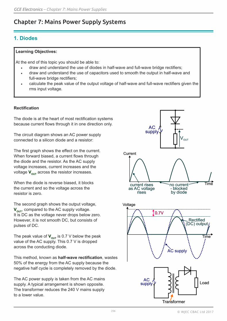
The circuit diagram shows an AC power supplyconnected to a silicon diode and a resistor:
The first graph shows the effect on the current. When forward biased, a current flows throughthe diode and the resistor. As the AC supplyvoltage increases, current increases and thevoltage VOUT across the resistor increases.
When the diode is reverse biased, it blocksthe current and so the voltage across theresistor is zero.
The second graph shows the output voltage,VOUT, compared to the AC supply voltage.It is DC as the voltage never drops below zero. However, it is not smooth DC, but consists ofpulses of DC.
The peak value of VOUT is 0.7 V below the peak value of the AC supply. This 0.7 V is dropped across the conducting diode.
This method, known as half-wave rectification, wastes 50% of the energy from the AC supply because the negative half cycle is completely removed by the diode.
The AC power supply is taken from the AC mainssupply. A typical arrangement is shown opposite.The transformer reduces the 240 V mains supplyto a lower value.
© WJEC CBAC Ltd 2017257
GCE Electronics – Chapter 7: Mains Power Supplies
Rms vs Peak Voltage
V0 = Vrms × 2
For example, suppose that the transformer secondary outputs a voltage of 12 V rms.The peak secondary voltage is: V0 = Vrms × 2 = 12 × 1.414 = 16.97 V (= ~17 V)
Taking into account the 0.7 V dropped across the diode when forward biased, the rectified output has a peak value of 17 V – 0.7 V = 16.3 V
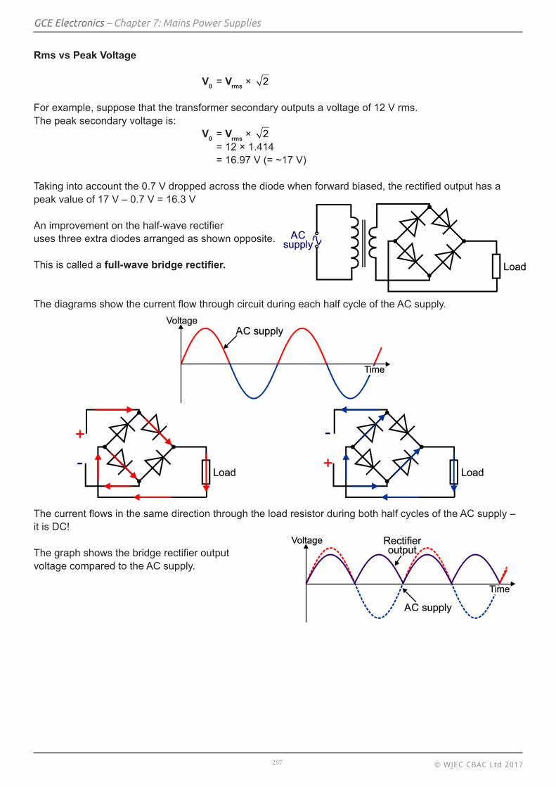
An improvement on the half-wave rectifieruses three extra diodes arranged as shown opposite.
This is called a full-wave bridge rectifier.
The diagrams show the current flow through circuit during each half cycle of the AC supply.
The current flows in the same direction through the load resistor during both half cycles of the AC supply – it is DC!
The graph shows the bridge rectifier outputvoltage compared to the AC supply.
© WJEC CBAC Ltd 2017258
GCE Electronics – Chapter 7: Mains Power Supplies
Note:
• The negative part of the AC graph has been flipped to provide a second positive pulse within the same cycle.
• The peak voltage across the resistor is 1.4 V less than peak of the input signal due to the voltage drop across the two conducting diodes.
Capacitive Smoothing
The process of rectification is the first stage of converting an AC supply into smooth DC.The outputs of both the half-wave and full-wave rectifiers are unsuitable for powering electronic circuits because of their ‘pulsing’ nature.
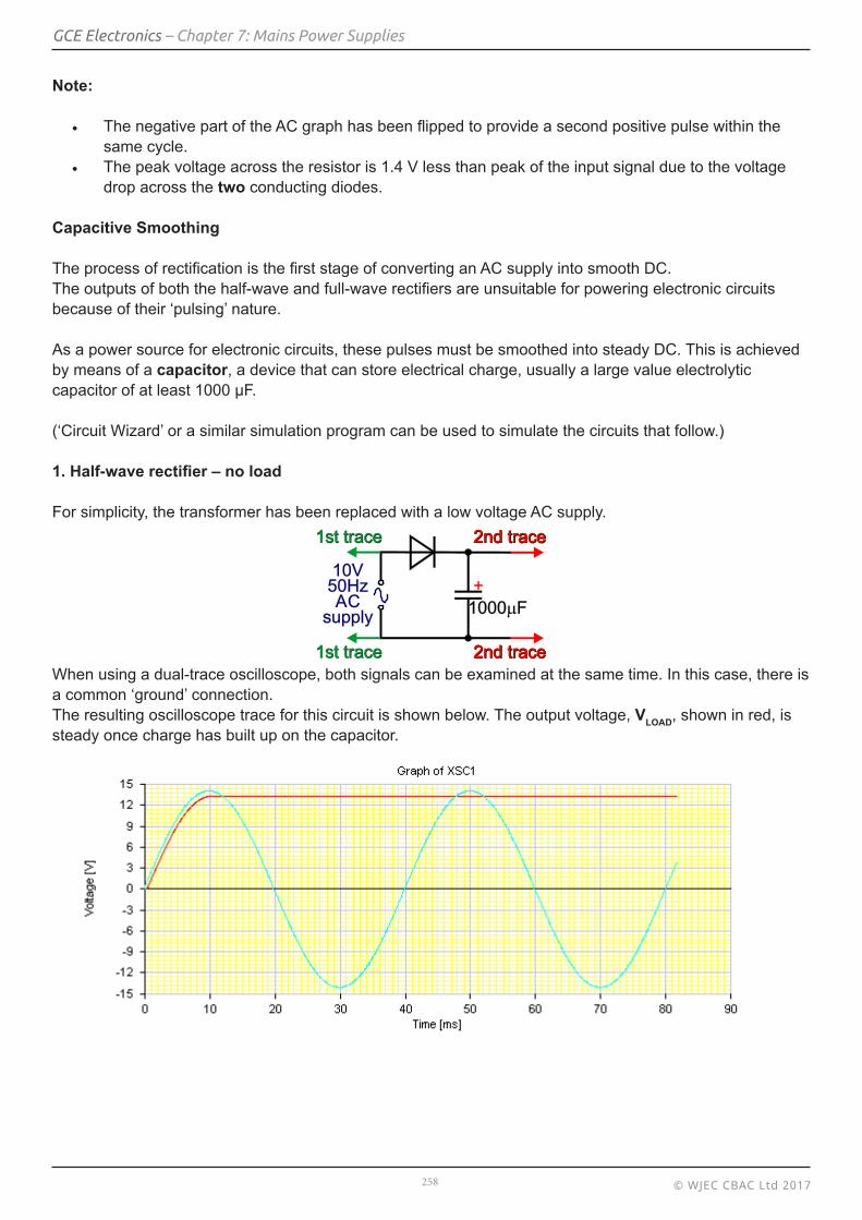
As a power source for electronic circuits, these pulses must be smoothed into steady DC. This is achieved by means of a capacitor, a device that can store electrical charge, usually a large value electrolytic capacitor of at least 1000 μF.
(‘Circuit Wizard’ or a similar simulation program can be used to simulate the circuits that follow.)
1. Half-wave rectifier – no load
For simplicity, the transformer has been replaced with a low voltage AC supply.
When using a dual-trace oscilloscope, both signals can be examined at the same time. In this case, there is a common ‘ground’ connection.The resulting oscilloscope trace for this circuit is shown below. The output voltage, VLOAD, shown in red, is steady once charge has built up on the capacitor.
© WJEC CBAC Ltd 2017259
GCE Electronics – Chapter 7: Mains Power Supplies
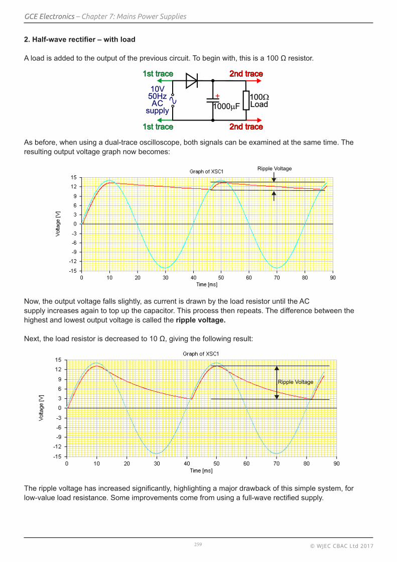
2. Half-wave rectifier – with load
A load is added to the output of the previous circuit. To begin with, this is a 100 Ω resistor.
As before, when using a dual-trace oscilloscope, both signals can be examined at the same time. The resulting output voltage graph now becomes:
Now, the output voltage falls slightly, as current is drawn by the load resistor until the ACsupply increases again to top up the capacitor. This process then repeats. The difference between the highest and lowest output voltage is called the ripple voltage.
Next, the load resistor is decreased to 10 Ω, giving the following result:
The ripple voltage has increased significantly, highlighting a major drawback of this simple system, for low-value load resistance. Some improvements come from using a full-wave rectified supply.
Ripple Voltage
Ripple Voltage
© WJEC CBAC Ltd 2017260
GCE Electronics – Chapter 7: Mains Power Supplies
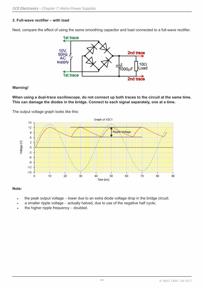
3. Full-wave rectifier – with load
Next, compare the effect of using the same smoothing capacitor and load connected to a full-wave rectifier.
Warning!
When using a dual-trace oscilloscope, do not connect up both traces to the circuit at the same time. This can damage the diodes in the bridge. Connect to each signal separately, one at a time.
The output voltage graph looks like this:
Note:
• the peak output voltage − lower due to an extra diode voltage drop in the bridge circuit;• a smaller ripple voltage − actually halved, due to use of the negative half cycle;• the higher ripple frequency − doubled.
Ripple Voltage
© WJEC CBAC Ltd 2017261
GCE Electronics – Chapter 7: Mains Power Supplies
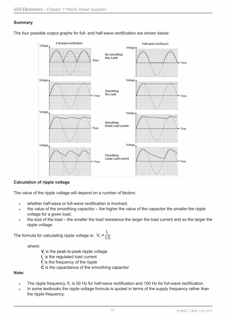
Summary
The four possible output graphs for full- and half-wave rectification are shown below:
Calculation of ripple voltage
The value of the ripple voltage will depend on a number of factors:
• whether half-wave or full-wave rectification is involved;• the value of the smoothing capacitor – the higher the value of the capacitor the smaller the ripple
voltage for a given load;• the size of the load – the smaller the load resistance the larger the load current and so the larger the
ripple voltage.
The formula for calculating ripple voltage is:
where: Vr is the peak-to-peak ripple voltage IL is the regulated load current fr is the frequency of the ripple C is the capacitance of the smoothing capacitorNote:
• The ripple frequency, fr, is 50 Hz for half-wave rectification and 100 Hz for full-wave rectification.• In some textbooks the ripple voltage formula is quoted in terms of the supply frequency rather than
the ripple frequency.
© WJEC CBAC Ltd 2017262
GCE Electronics – Chapter 7: Mains Power Supplies
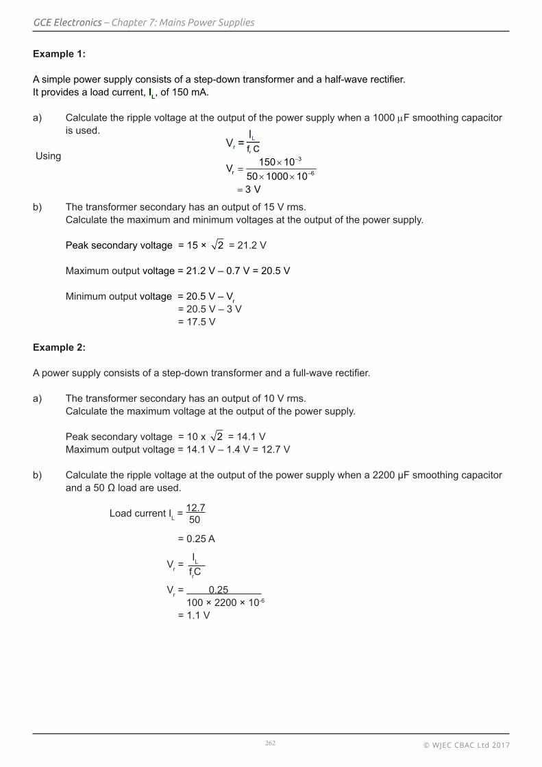
Example 1:
A simple power supply consists of a step-down transformer and a half-wave rectifier.It provides a load current, IL, of 150 mA.
a) Calculate the ripple voltage at the output of the power supply when a 1000 µF smoothing capacitor is used.
Using
b) The transformer secondary has an output of 15 V rms. Calculate the maximum and minimum voltages at the output of the power supply.
Peak secondary voltage = 15 × 2 = 21.2 V
Maximum output voltage = 21.2 V – 0.7 V = 20.5 V
Minimum output voltage = 20.5 V – Vr = 20.5 V – 3 V = 17.5 V
Example 2:
A power supply consists of a step-down transformer and a full-wave rectifier.
a) The transformer secondary has an output of 10 V rms. Calculate the maximum voltage at the output of the power supply.
Peak secondary voltage = 10 x 2 = 14.1 V Maximum output voltage = 14.1 V – 1.4 V = 12.7 V
b) Calculate the ripple voltage at the output of the power supply when a 2200 µF smoothing capacitor and a 50 Ω load are used.
Load current IL = 12.7
50
= 0.25 A
Vr = IL
frC
Vr = 0.25 100 × 2200 × 10-6
= 1.1 V
3
r 6
150 10V50 1000 10
3 V
−
−
×=
× ×=
© WJEC CBAC Ltd 2017263
GCE Electronics – Chapter 7: Mains Power Supplies
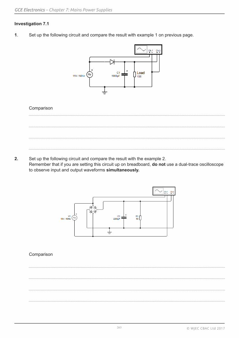
Investigation 7.1
1. Set up the following circuit and compare the result with example 1 on previous page.
Comparison
2. Set up the following circuit and compare the result with the example 2. Remember that if you are setting this circuit up on breadboard, do not use a dual-trace oscilloscope to observe input and output waveforms simultaneously.
Comparison
© WJEC CBAC Ltd 2017264
GCE Electronics – Chapter 7: Mains Power Supplies
Exercise 7.1
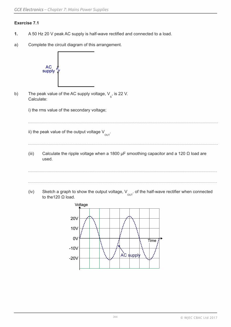
1. A 50 Hz 20 V peak AC supply is half-wave rectified and connected to a load.
a) Complete the circuit diagram of this arrangement.
b) The peak value of the AC supply voltage, VS, is 22 V.
Calculate:
i) the rms value of the secondary voltage;
ii) the peak value of the output voltage VOUT
.
(iii) Calculate the ripple voltage when a 1800 µF smoothing capacitor and a 120 Ω load are used.
(iv) Sketch a graph to show the output voltage, VOUT
. of the half-wave rectifier when connected to the120 Ω load.
© WJEC CBAC Ltd 2017265
GCE Electronics – Chapter 7: Mains Power Supplies
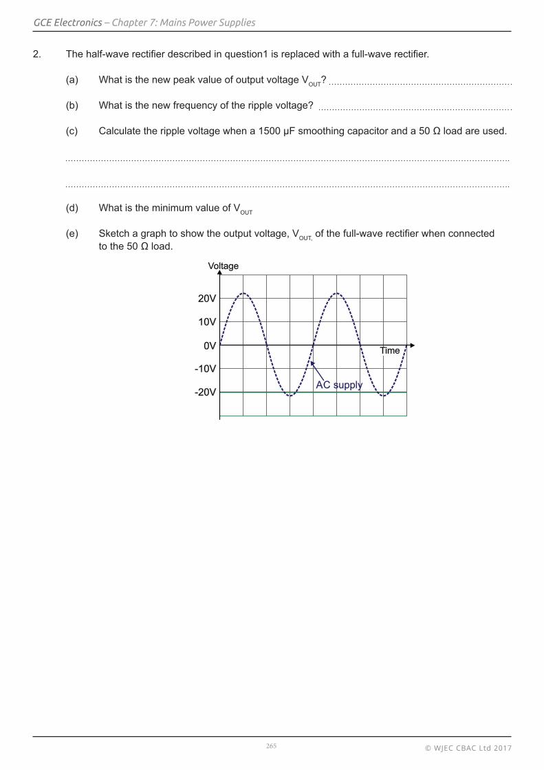
2. The half-wave rectifier described in question1 is replaced with a full-wave rectifier.
(a) What is the new peak value of output voltage VOUT?
(b) What is the new frequency of the ripple voltage?
(c) Calculate the ripple voltage when a 1500 µF smoothing capacitor and a 50 Ω load are used.
(d) What is the minimum value of VOUT
(e) Sketch a graph to show the output voltage, VOUT, of the full-wave rectifier when connected to the 50 Ω load.
© WJEC CBAC Ltd 2017266
GCE Electronics – Chapter 7: Mains Power Supplies
2. Voltage Regulation
Learning Objectives:
At the end of this topic you should be able to:• draw the circuit diagram for a voltage regulator based on a zener diode;• design a voltage regulator, based on a zener diode, to meet a given specification;• calculate the maximum output current available from a given voltage regulator;• calculate the power rating needed by the zener diode and series resistor in a given voltage
regulator.
For many circuits, it is desirable to have a power supply which gives out a constant voltage regardless of the current it is delivering.
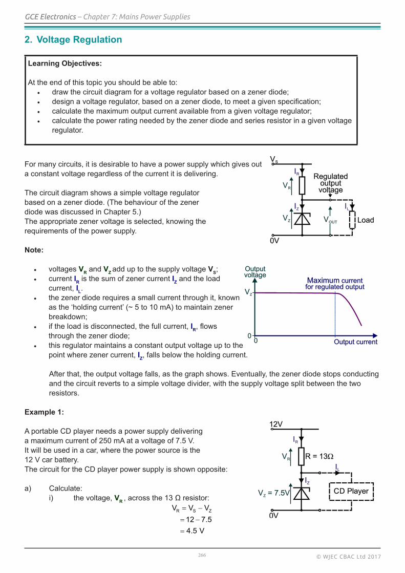
The circuit diagram shows a simple voltage regulatorbased on a zener diode. (The behaviour of the zenerdiode was discussed in Chapter 5.)The appropriate zener voltage is selected, knowing therequirements of the power supply.
Note:
• voltages VR and VZ add up to the supply voltage VS;• current IR is the sum of zener current IZ and the load
current, IL.• the zener diode requires a small current through it, known
as the ‘holding current’ (~ 5 to 10 mA) to maintain zener breakdown;
• if the load is disconnected, the full current, IR, flows through the zener diode;
• this regulator maintains a constant output voltage up to the point where zener current, IZ, falls below the holding current.
After that, the output voltage falls, as the graph shows. Eventually, the zener diode stops conducting and the circuit reverts to a simple voltage divider, with the supply voltage split between the two resistors.
Example 1:
A portable CD player needs a power supply deliveringa maximum current of 250 mA at a voltage of 7.5 V.It will be used in a car, where the power source is the12 V car battery.The circuit for the CD player power supply is shown opposite:
a) Calculate: i) the voltage, VR , across the 13 Ω resistor:
R S ZV V V 12 7.5 4.5 V
= −
= −=
© WJEC CBAC Ltd 2017267
GCE Electronics – Chapter 7: Mains Power Supplies
ii) the current, IR, through the 13 Ω resistor
iii) the zener current, IZ, when the load current IL = 250 mA
b) Calculate the minimum power rating for the 13 Ω resistor from the values: 1 W 2 W 3 W
Therefore, we choose a 2 W resistor.
c) The car battery charges up to 13.8 V after a long journey. What is the new output voltage?
Output voltage = 7.5 V (but VR increases by 1.8 V to 6.3 V).
Example 2:
The 6.2 V stabilised power supply shown opposite mustprovide a maximum load current, IL, of 300 mA.The zener diode requires a holding current of 10 mA.
a) Calculate the preferred value of resistor R:
The E24 resistor series does not have a 28.4 Ω resistor. The nearest values are 27 Ω and 33 Ω.Choosing the 33 Ω resistor would reduce the current to below 310 mA. This would not allow a current of 300 mA for the CD player whilst maintaining the zener in reverse breakdown by passing a current of 10 mA through it.The 27 Ω resistor therefore must be used. This allows more current than required through the resistor. The excess flows through the zener diode. In fact, the current through the 27 Ω resistor would be:
This increases power dissipation in both the resistor R and the zener diode.
RR
VIR4.5 13
0.346 A 346 mA
=
=
= =
Z R LI I I 346 250 96 mA
= −
= −=
R R RP I V 346 4.5 1557 mW 1.557 W
= ×
= ×= =
R
R
VRI8.8 310
0.0284 k 28.4
=
=
= Ω = Ω
R S ZV V V 15 6.2 8.8 V
= −
= −=
R Z LI I I 10 300 310 mA
= +
= +=
RR
VIR8.8 27
0.326 A 326 mA
=
=
= =
© WJEC CBAC Ltd 2017268
GCE Electronics – Chapter 7: Mains Power Supplies
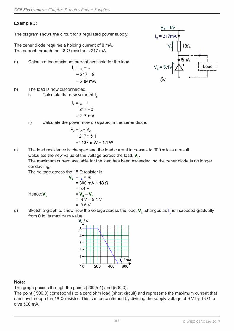
Example 3:
The diagram shows the circuit for a regulated power supply.
The zener diode requires a holding current of 8 mA.The current through the 18 Ω resistor is 217 mA.
a) Calculate the maximum current available for the load.
b) The load is now disconnected. i) Calculate the new value of IZ.
ii) Calculate the power now dissipated in the zener diode.
c) The load resistance is changed and the load current increases to 300 mA as a result. Calculate the new value of the voltage across the load, VL. The maximum current available for the load has been exceeded, so the zener diode is no longer conducting. The voltage across the 18 Ω resistor is: VR = IR × R = 300 mA × 18 Ω = 5.4 V Hence: VL = VS – VR = 9 V – 5.4 V = 3.6 Vd) Sketch a graph to show how the voltage across the load, VL, changes as IL is increased gradually from 0 to its maximum value.
Note: The graph passes through the points (209,5.1) and (500,0).The point ( 500,0) corresponds to a zero ohm load (short circuit) and represents the maximum current that can flow through the 18 Ω resistor. This can be confirmed by dividing the supply voltage of 9 V by 18 Ω to give 500 mA.
L R ZI I I 217 8 209 mA
= −
= −=
Z R LI I I 217 0 217 mA
= −
= −=
Z Z ZP I V 217 5.1 1107 mW 1.1 W
= ×
= ×= =
© WJEC CBAC Ltd 2017269
GCE Electronics – Chapter 7: Mains Power Supplies
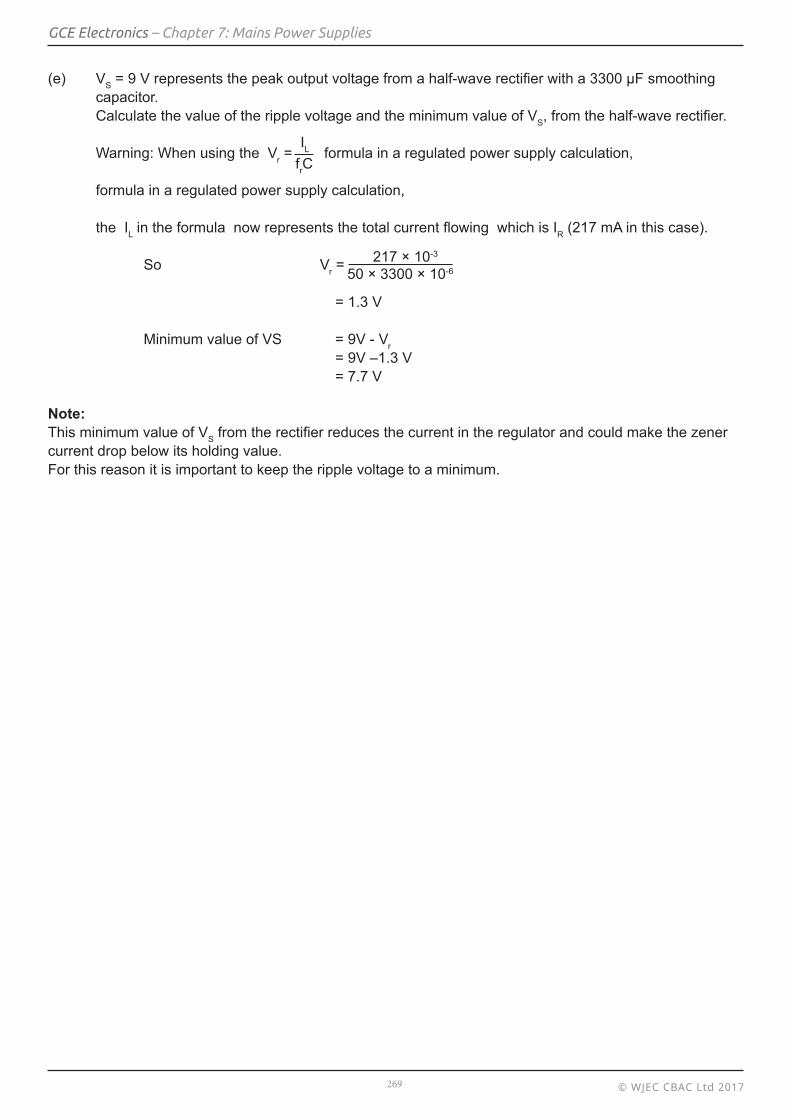
(e) VS = 9 V represents the peak output voltage from a half-wave rectifier with a 3300 µF smoothing capacitor. Calculate the value of the ripple voltage and the minimum value of VS, from the half-wave rectifier.
Warning: When using the Vr = IL formula in a regulated power supply calculation,
frC
formula in a regulated power supply calculation,
the IL in the formula now represents the total current flowing which is IR (217 mA in this case).
So Vr = 217 × 10-3
50 × 3300 × 10-6
= 1.3 V
Minimum value of VS = 9V - Vr = 9V –1.3 V = 7.7 V
Note: This minimum value of VS from the rectifier reduces the current in the regulator and could make the zener current drop below its holding value. For this reason it is important to keep the ripple voltage to a minimum.
© WJEC CBAC Ltd 2017270
GCE Electronics – Chapter 7: Mains Power Supplies
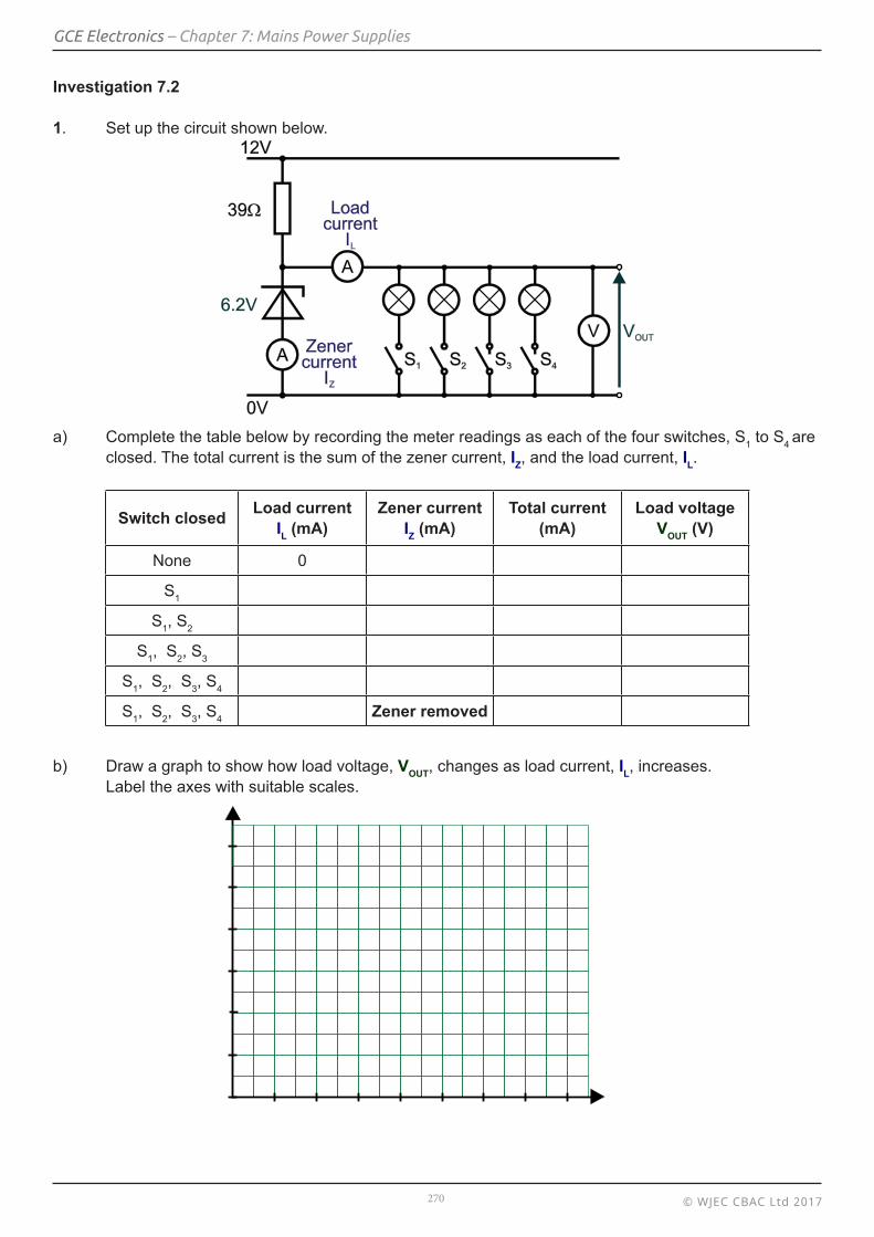
Investigation 7.2
1. Set up the circuit shown below.
a) Complete the table below by recording the meter readings as each of the four switches, S1 to S4 are closed. The total current is the sum of the zener current, IZ, and the load current, IL.
Switch closed Load current IL (mA)
Zener current IZ (mA)
Total current (mA)
Load voltageVOUT (V)
None 0
S1
S1, S2
S1, S2, S3
S1, S2, S3, S4
S1, S2, S3, S4 Zener removed
b) Draw a graph to show how load voltage, VOUT, changes as load current, IL, increases. Label the axes with suitable scales.
© WJEC CBAC Ltd 2017271
GCE Electronics – Chapter 7: Mains Power Supplies
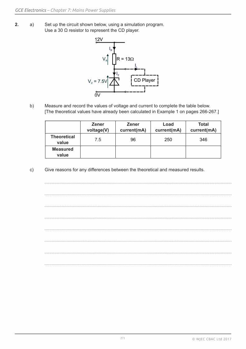
2. a) Set up the circuit shown below, using a simulation program. Use a 30 Ω resistor to represent the CD player.
b) Measure and record the values of voltage and current to complete the table below. [The theoretical values have already been calculated in Example 1 on pages 266-267.]
Zenervoltage(V)
Zener current(mA)
Load current(mA)
Total current(mA)
Theoretical value 7.5 96 250 346
Measured value
c) Give reasons for any differences between the theoretical and measured results.
© WJEC CBAC Ltd 2017272
GCE Electronics – Chapter 7: Mains Power Supplies
Exercise 7.2
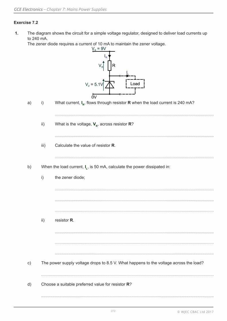
1. The diagram shows the circuit for a simple voltage regulator, designed to deliver load currents up to 240 mA. The zener diode requires a current of 10 mA to maintain the zener voltage.
a) i) What current, IR, flows through resistor R when the load current is 240 mA?
ii) What is the voltage, VR, across resistor R?
iii) Calculate the value of resistor R.
b) When the load current, IL, is 50 mA, calculate the power dissipated in:
i) the zener diode;
ii) resistor R.
c) The power supply voltage drops to 8.5 V. What happens to the voltage across the load?
d) Choose a suitable preferred value for resistor R?
© WJEC CBAC Ltd 2017273
GCE Electronics – Chapter 7: Mains Power Supplies
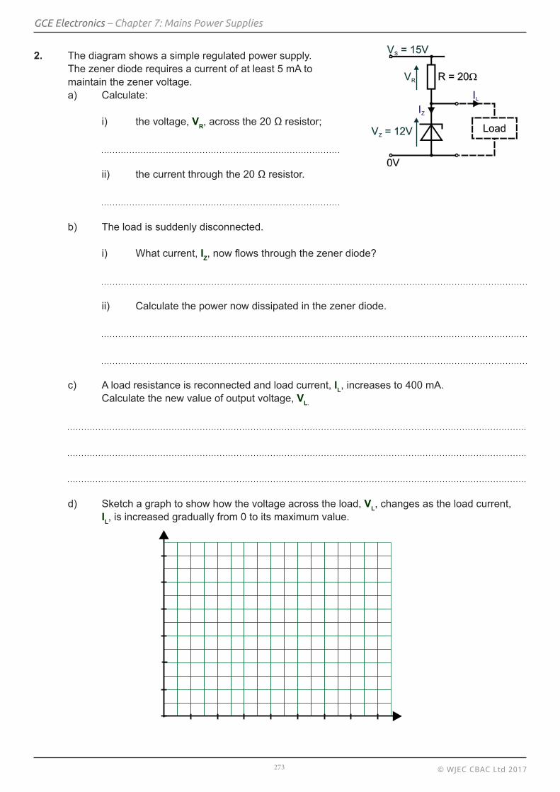
2. The diagram shows a simple regulated power supply. The zener diode requires a current of at least 5 mA to maintain the zener voltage. a) Calculate:
i) the voltage, VR, across the 20 Ω resistor;
ii) the current through the 20 Ω resistor.
b) The load is suddenly disconnected.
i) What current, IZ, now flows through the zener diode?
ii) Calculate the power now dissipated in the zener diode.
c) A load resistance is reconnected and load current, IL, increases to 400 mA. Calculate the new value of output voltage, VL.
d) Sketch a graph to show how the voltage across the load, VL, changes as the load current, IL, is increased gradually from 0 to its maximum value.
© WJEC CBAC Ltd 2017274
GCE Electronics – Chapter 7: Mains Power Supplies
(e) VS = 15 V represents the peak output voltage from a full-wave rectifier with a 3900 µF smoothing capacitor. Calculate the value of the ripple voltage produced when the zener current is 20 mA
© WJEC CBAC Ltd 2017275
GCE Electronics – Chapter 7: Mains Power Supplies
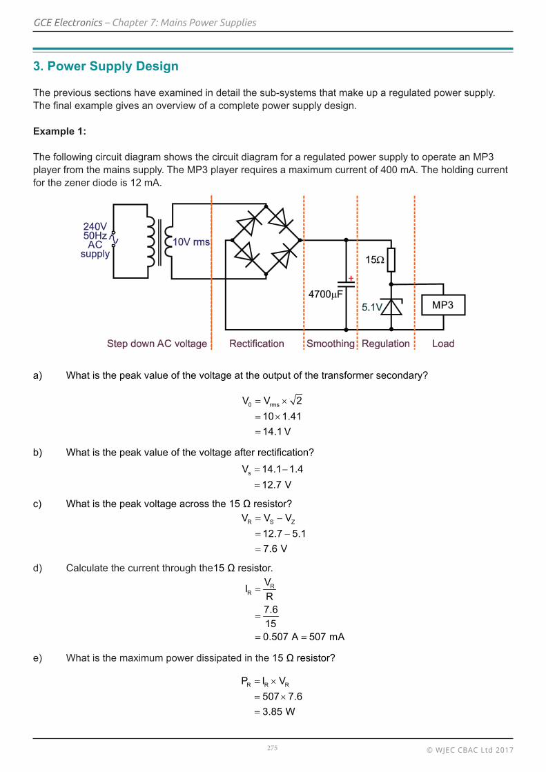
3. Power Supply Design
The previous sections have examined in detail the sub-systems that make up a regulated power supply. The final example gives an overview of a complete power supply design.
Example 1:
The following circuit diagram shows the circuit diagram for a regulated power supply to operate an MP3 player from the mains supply. The MP3 player requires a maximum current of 400 mA. The holding current for the zener diode is 12 mA.
a) What is the peak value of the voltage at the output of the transformer secondary?
b) What is the peak value of the voltage after rectification?
c) What is the peak voltage across the 15 Ω resistor?
d) Calculate the current through the15 Ω resistor.
e) What is the maximum power dissipated in the 15 Ω resistor?
0 rmsV V 2 10 1.41 14.1 V
= ×
= ×=
sV 14.1 1.4 12.7 V
= −
=
R S ZV V V 12.7 5.1 7.6 V
= −
= −=
RR
VIR7.6 15
0.507 A 507 mA
=
=
= =
R R RP I V 507 7.6 3.85 W
= ×
= ×=
© WJEC CBAC Ltd 2017276
GCE Electronics – Chapter 7: Mains Power Supplies
f) What is the current flowing through the zener diode when the MP3 player is drawing the full 400 mA from the supply? IZ = IR − IL = 507 − 400 = 107 mAg) What is the power dissipated in the zener diode when the current through the MP3 player is 400 mA. PZ = IZ −Vz = 107 − 5.1 = 546 mWh) The MP3 Player is now disconnected. What is the power dissipation in the zener diode? PZ = IZ −Vz = 507 − 5.1 = 2586 mW = 2.6 Wi) Calculate the ripple voltage across the smoothing circuit. (Remember that IR = 507 mA must be used in the equation)
Vr = IL
frC
Vr = 507 × 10-3
100 × 4700 × 10-6
= 1.1 V j) Calculate the minimum values of VR and IR when the value of the voltage after rectification is at its minimum. VS = 14.1 - 1.1 = 11.6 V Minimum VR = Vs - Vz = 11.6 - 5.1 = 6.5 V
IR = VR
R
= 6.5
15
= 0.433 A = 433 mA
k) Describe how the ripple voltage affects the voltage and current in the regulation/load section of the power supply when the load current is 400 mA.
The 1.1 V fluctuation in Vs would be absorbed across a 15 Ω resistor. This would cause the current through the 15 Ω resistor to pulse between 433 - 507 mA, and the zener current to pulse between 33 and 107 mA at a frequency of 100 Hz.
The 33 mA minimum current through the zener is far in excess of the 12 mA holding current so the 5.1 V zener voltage is maintained.
The load current will remain constant at 400 mA.
Note: The answers to parts e) and h) above illustrate the limitations of the zener dioderegulated power supply in terms of the power dissipated in the components.
© WJEC CBAC Ltd 2017277
GCE Electronics – Chapter 7: Mains Power Supplies
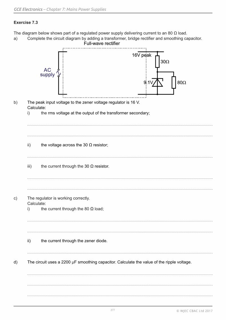
Exercise 7.3
The diagram below shows part of a regulated power supply delivering current to an 80 Ω load. a) Complete the circuit diagram by adding a transformer, bridge rectifier and smoothing capacitor.
b) The peak input voltage to the zener voltage regulator is 16 V. Calculate: i) the rms voltage at the output of the transformer secondary;
ii) the voltage across the 30 Ω resistor;
iii) the current through the 30 Ω resistor.
c) The regulator is working correctly. Calculate: i) the current through the 80 Ω load;
ii) the current through the zener diode.
d) The circuit uses a 2200 µF smoothing capacitor. Calculate the value of the ripple voltage.
© WJEC CBAC Ltd 2017278
GCE Electronics – Chapter 7: Mains Power Supplies
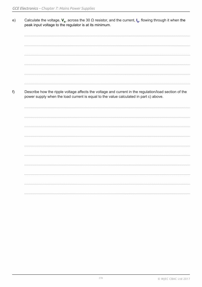
e) Calculate the voltage, VR, across the 30 Ω resistor, and the current, IR, flowing through it when the peak input voltage to the regulator is at its minimum.
f) Describe how the ripple voltage affects the voltage and current in the regulation/load section of the power supply when the load current is equal to the value calculated in part c) above.