Embed Size (px)
Citation preview

8/11/2019 Chapter 8 Ion Implantation _ I (3)
http://slidepdf.com/reader/full/chapter-8-ion-implantation-i-3 1/40
1. Introduction and application.
2. Ion implantation tools.
3. Dopant distribution.
4. Mask thickness and lateral distribution.
5. Effect of channeling.
6. Damage caused by ion implantation.
7. Damage repair.
Chapter 8 Ion implantation
1
NE 343: Microfabrication and thin film technologyInstructor: Bo Cui, ECE, University of Waterloo; http://ece.uwaterloo.ca/~bcui/Textbook: Silicon VLSI Technology by Plummer, Deal and Griffin
8/11/2019 Chapter 8 Ion Implantation _ I (3)
http://slidepdf.com/reader/full/chapter-8-ion-implantation-i-3 2/40
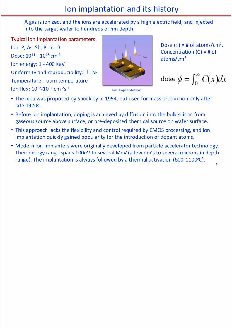
A gas is ionized, and the ions are accelerated by a high electric field, and injectedinto the target wafer to hundreds of nm depth.
Ion implantation and its history
Typical ion implantation parameters:Ion: P, As, Sb, B, In, ODose: 10 11 - 1018 cm -2
Ion energy: 1 - 400 keVUniformity and reproducibility: ± 1%
Temperature: room temperatureIon flux: 10 12-1014 cm -2s-1
Dose ( ) = # of atoms/cm 2.Concentration (C) = # ofatoms/cm 3.
• The idea was proposed by Shockley in 1954, but used for mass production only afterlate 1970s.
• Before ion implantation, doping is achieved by diffusion into the bulk silicon from
gaseous source above surface, or pre-deposited chemical source on wafer surface.• This approach lacks the flexibility and control required by CMOS processing, and ion
implantation quickly gained popularity for the introduction of dopant atoms.• Modern ion implanters were originally developed from particle accelerator technology.
Their energy range spans 100eV to several MeV (a few nm’s to several microns in depth
range). The implantation is always followed by a thermal activation (600-1100o
C). 2
8/11/2019 Chapter 8 Ion Implantation _ I (3)
http://slidepdf.com/reader/full/chapter-8-ion-implantation-i-3 3/40
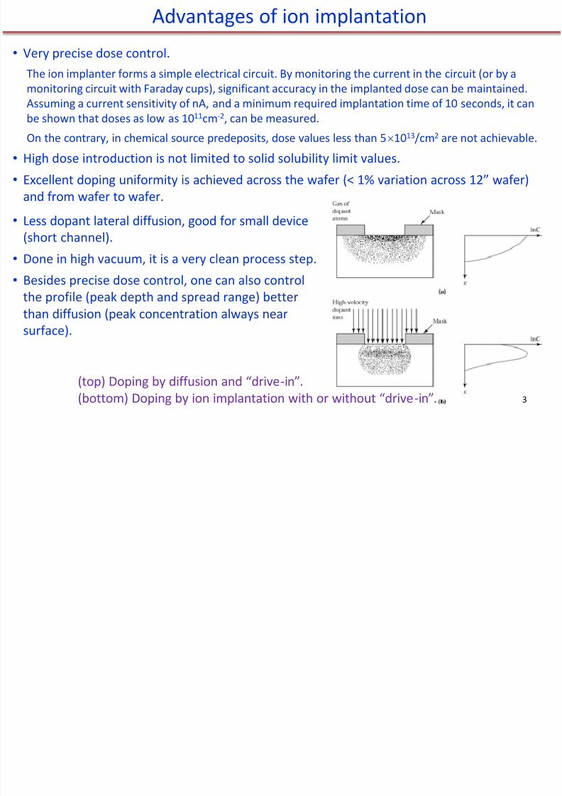
Advantages of ion implantation• Very precise dose control.
The ion implanter forms a simple electrical circuit. By monitoring the current in the circuit (or by amonitoring circuit with Faraday cups), significant accuracy in the implanted dose can be maintained.Assuming a current sensitivity of nA, and a minimum required implantation time of 10 seconds, it canbe shown that doses as low as 10 11cm -2, can be measured.
On the contrary, in chemical source predeposits, dose values less than 5 1013/cm 2 are not achievable.• High dose introduction is not limited to solid solubility limit values.• Excellent doping uniformity is achieved across the wafer (< 1% variation across 12” wafer)
and from wafer to wafer.• Less dopant lateral diffusion, good for small device
(short channel).• Done in high vacuum, it is a very clean process step.• Besides precise dose control, one can also control
the profile (peak depth and spread range) betterthan diffusion (peak concentration always nearsurface).
(top) Doping by diffusion and “drive -in”. (bottom) Doping by ion implantation with or without “drive -in”. 3
8/11/2019 Chapter 8 Ion Implantation _ I (3)
http://slidepdf.com/reader/full/chapter-8-ion-implantation-i-3 4/40
8/11/2019 Chapter 8 Ion Implantation _ I (3)
http://slidepdf.com/reader/full/chapter-8-ion-implantation-i-3 5/40
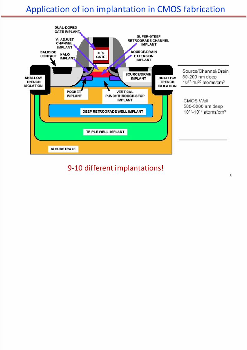
Application of ion implantation in CMOS fabrication
9-10 different implantations!5
8/11/2019 Chapter 8 Ion Implantation _ I (3)
http://slidepdf.com/reader/full/chapter-8-ion-implantation-i-3 6/40
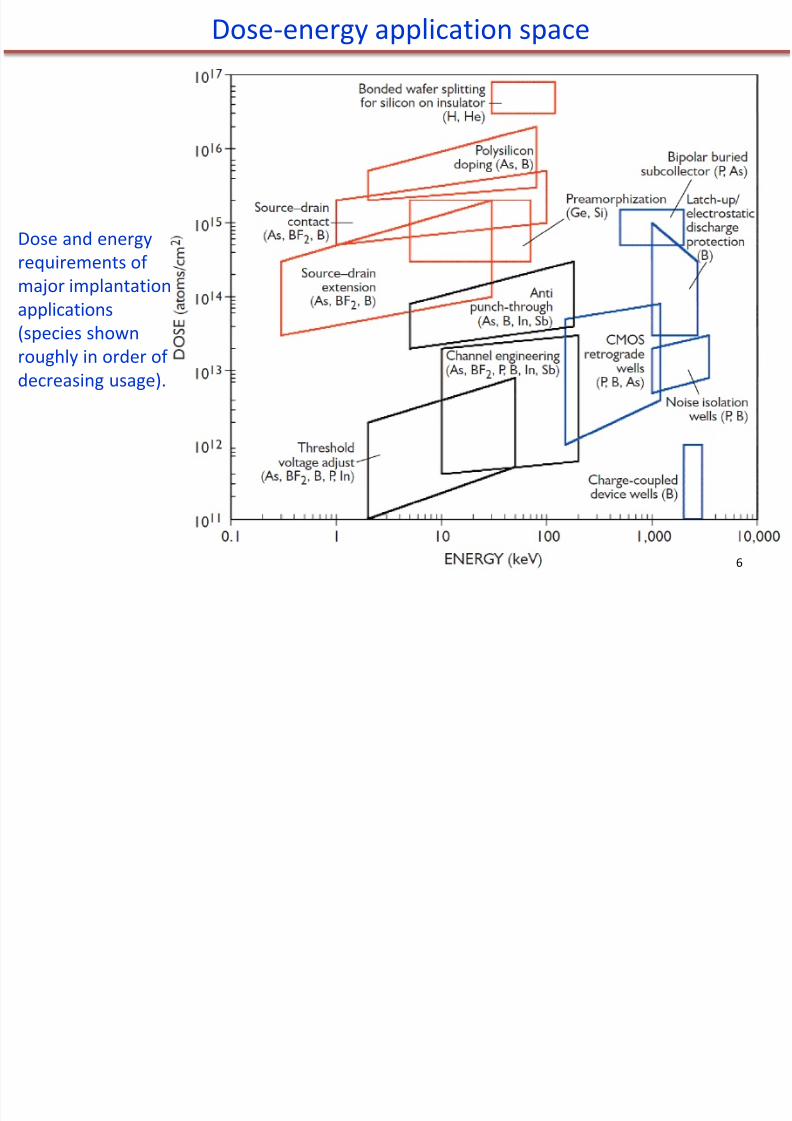
Dose-energy application space
6
Dose and energyrequirements ofmajor implantationapplications(species shownroughly in order ofdecreasing usage).
8/11/2019 Chapter 8 Ion Implantation _ I (3)
http://slidepdf.com/reader/full/chapter-8-ion-implantation-i-3 7/40
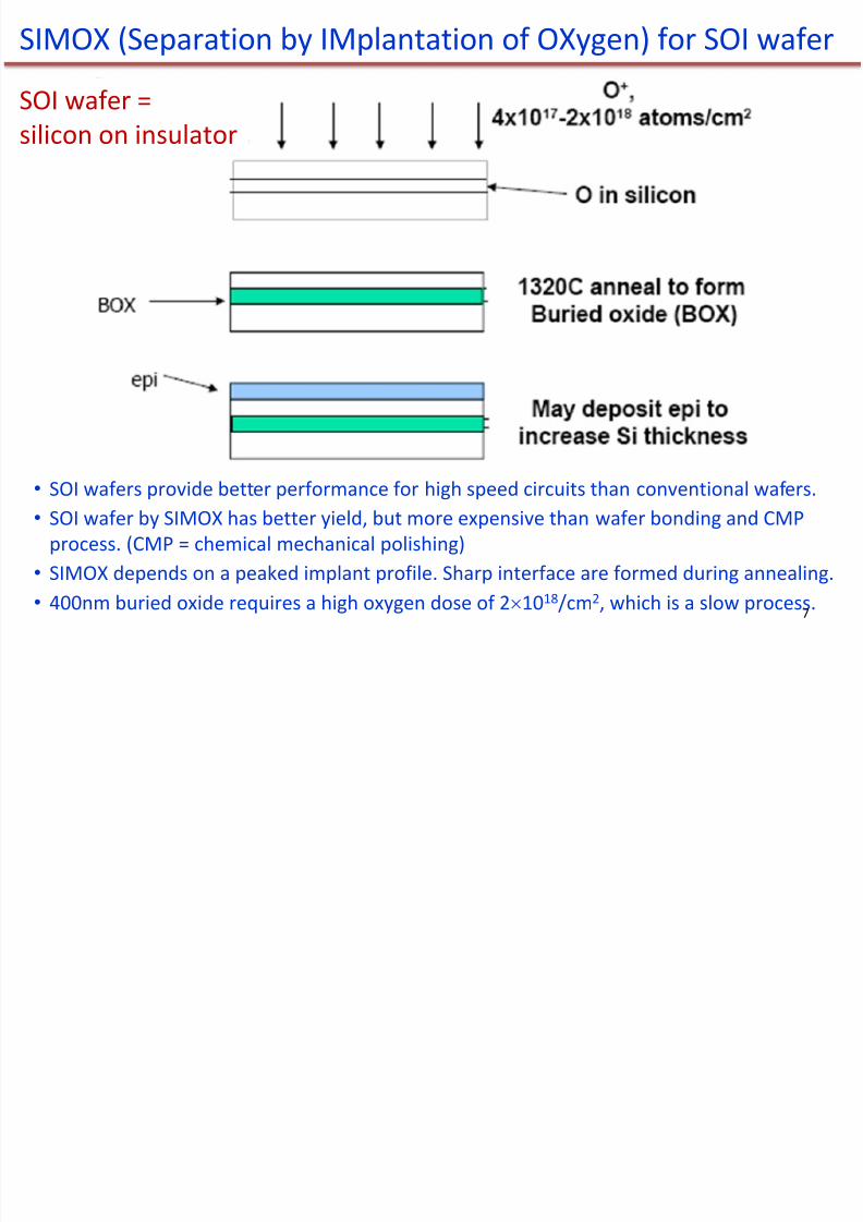
SIMOX (Separation by IMplantation of OXygen) for SOI wafer
• SOI wafers provide better performance for high speed circuits than conventional wafers.• SOI wafer by SIMOX has better yield, but more expensive than wafer bonding and CMP
process. (CMP = chemical mechanical polishing)• SIMOX depends on a peaked implant profile. Sharp interface are formed during annealing.• 400nm buried oxide requires a high oxygen dose of 2 1018/cm 2, which is a slow process.
SOI wafer =silicon on insulator
7
8/11/2019 Chapter 8 Ion Implantation _ I (3)
http://slidepdf.com/reader/full/chapter-8-ion-implantation-i-3 8/40
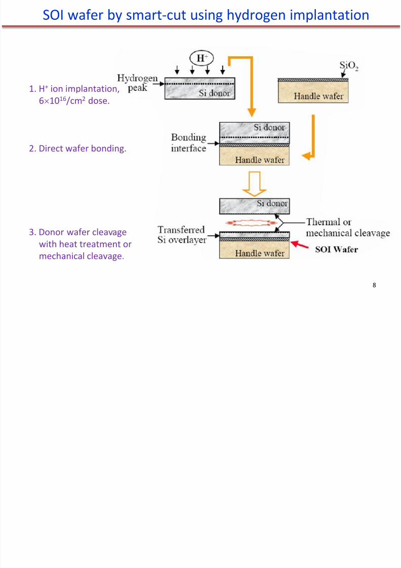
SOI wafer by smart-cut using hydrogen implantation
1. H+ ion implantation,6 1016/cm 2 dose.
2. Direct wafer bonding.
3. Donor wafer cleavagewith heat treatment ormechanical cleavage.
8
8/11/2019 Chapter 8 Ion Implantation _ I (3)
http://slidepdf.com/reader/full/chapter-8-ion-implantation-i-3 9/40
1. Introduction and application.
2. Ion implantation tools.
3. Dopant distribution.
4. Mask thickness and lateral distribution.
5. Effect of channeling.
6. Damage caused by ion implantation.
7. Damage repair.
Chapter 8 Ion implantation
NE 343: Microfabrication and Thin Film TechnologyInstructor: Bo Cui, ECE, University of Waterloo, [email protected]: Silicon VLSI Technology by Plummer, Deal, Griffin
9
8/11/2019 Chapter 8 Ion Implantation _ I (3)
http://slidepdf.com/reader/full/chapter-8-ion-implantation-i-3 10/40
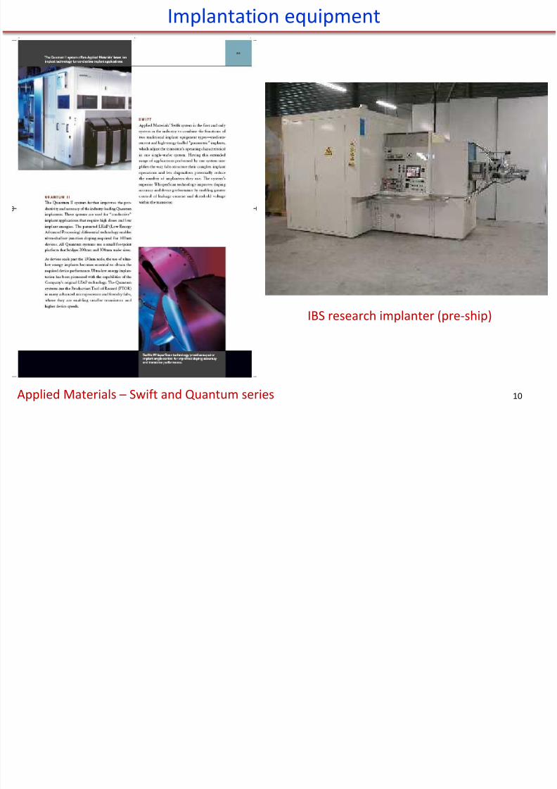
Implantation equipment
Applied Materials – Swift and Quantum series
IBS research implanter (pre-ship)
10
8/11/2019 Chapter 8 Ion Implantation _ I (3)
http://slidepdf.com/reader/full/chapter-8-ion-implantation-i-3 11/40
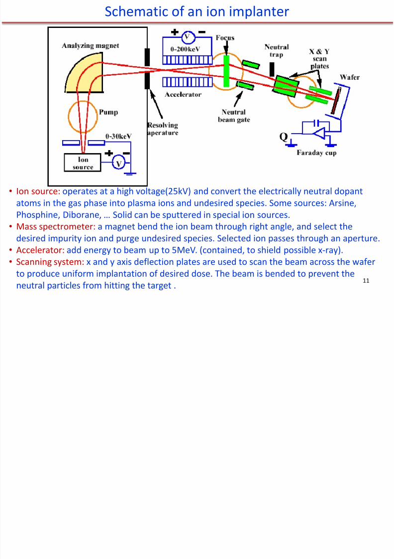
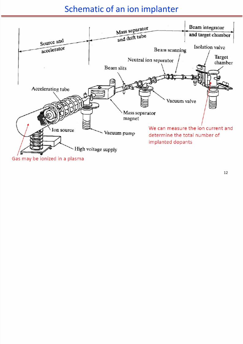
Schematic of an ion implanter
• Ion source: operates at a high voltage(25kV) and convert the electrically neutral dopant
atoms in the gas phase into plasma ions and undesired species. Some sources: Arsine,Phosphine, Diborane , … Solid can be sputtered in special ion sources. • Mass spectrometer: a magnet bend the ion beam through right angle, and select the
desired impurity ion and purge undesired species. Selected ion passes through an aperture.• Accelerator: add energy to beam up to 5MeV. (contained, to shield possible x-ray).• Scanning system: x and y axis deflection plates are used to scan the beam across the wafer
to produce uniform implantation of desired dose. The beam is bended to prevent theneutral particles from hitting the target .11
8/11/2019 Chapter 8 Ion Implantation _ I (3)
http://slidepdf.com/reader/full/chapter-8-ion-implantation-i-3 12/40
Schematic of an ion implanter
12
8/11/2019 Chapter 8 Ion Implantation _ I (3)
http://slidepdf.com/reader/full/chapter-8-ion-implantation-i-3 13/40
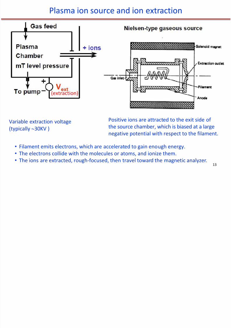
Variable extraction voltage(typically 30KV )
Positive ions are attracted to the exit side ofthe source chamber, which is biased at a largenegative potential with respect to the filament.
Plasma ion source and ion extraction
• Filament emits electrons, which are accelerated to gain enough energy.• The electrons collide with the molecules or atoms, and ionize them.•
The ions are extracted, rough-focused, then travel toward the magnetic analyzer.
(extraction)
13
8/11/2019 Chapter 8 Ion Implantation _ I (3)
http://slidepdf.com/reader/full/chapter-8-ion-implantation-i-3 14/40
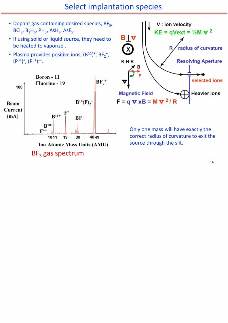
Select implantation species
Only one mass will have exactly thecorrect radius of curvature to exit thesource through the slit.
BF3 gas spectrum
• Dopant gas containing desired species, BF 3,BCl3, B2H6, PH3, AsH3, AsF5.
•
If using solid or liquid source, they need tobe heated to vaporize .• Plasma provides positive ions, (B 11)+, BF2
+,(P31)+, (P31)++.
14
8/11/2019 Chapter 8 Ion Implantation _ I (3)
http://slidepdf.com/reader/full/chapter-8-ion-implantation-i-3 15/40
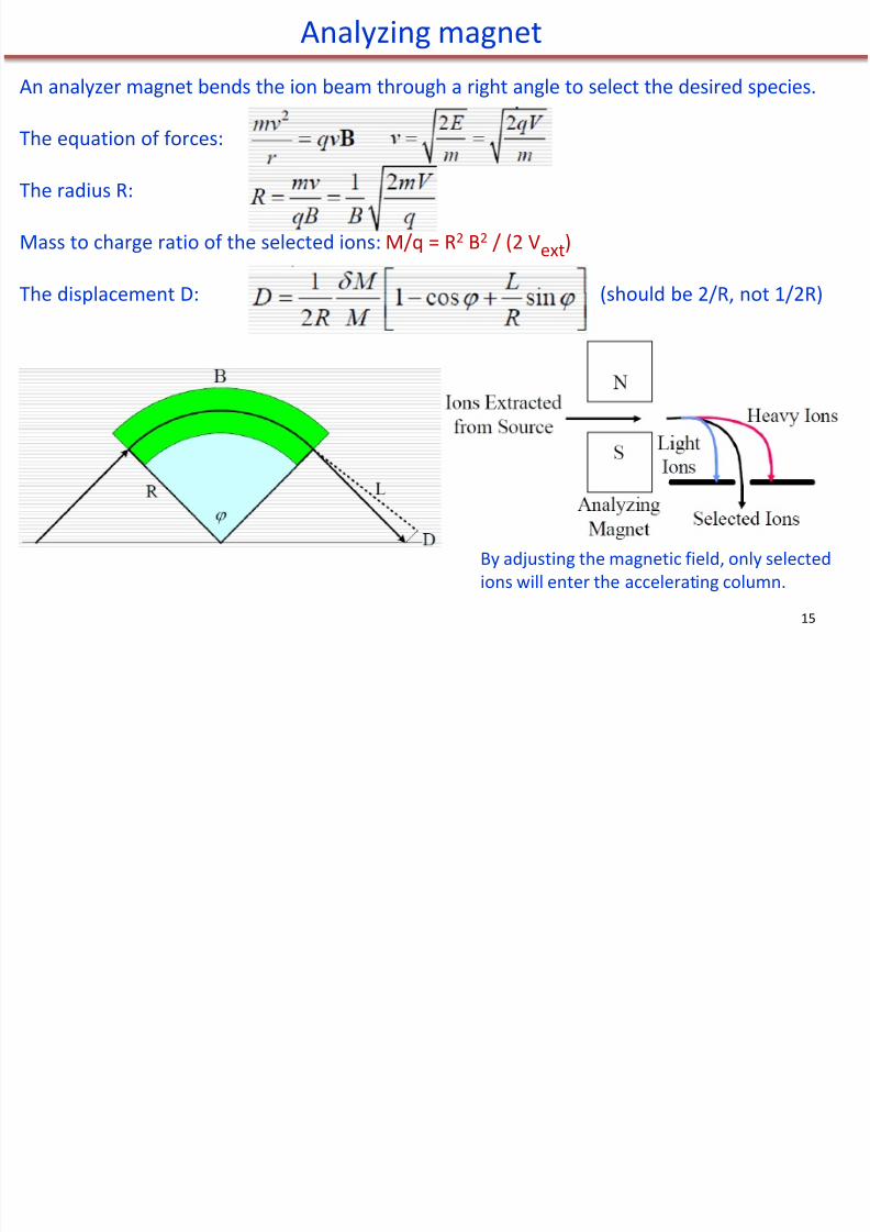
Analyzing magnet
An analyzer magnet bends the ion beam through a right angle to select the desired species.
The equation of forces:
The radius R:
Mass to charge ratio of the selected ions: M/q = R 2 B2 / (2 Vext )
The displacement D: (should be 2/R, not 1/2R)
By adjusting the magnetic field, only selectedions will enter the accelerating column.
15
8/11/2019 Chapter 8 Ion Implantation _ I (3)
http://slidepdf.com/reader/full/chapter-8-ion-implantation-i-3 16/40
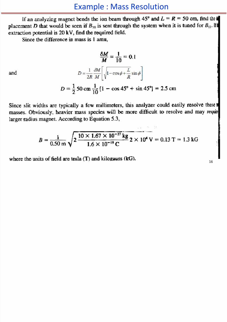
Example : Mass Resolution
16
8/11/2019 Chapter 8 Ion Implantation _ I (3)
http://slidepdf.com/reader/full/chapter-8-ion-implantation-i-3 17/40
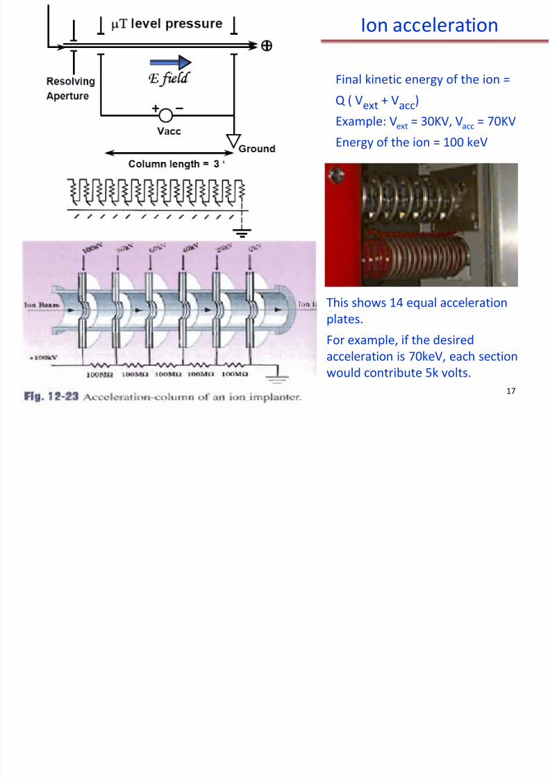
Final kinetic energy of the ion =
Q ( Vext + Vacc)Example: Vext = 30KV, Vacc = 70KV
Energy of the ion = 100 keV
Ion acceleration
This shows 14 equal accelerationplates.
For example, if the desiredacceleration is 70keV, each sectionwould contribute 5k volts.
17
8/11/2019 Chapter 8 Ion Implantation _ I (3)
http://slidepdf.com/reader/full/chapter-8-ion-implantation-i-3 18/40
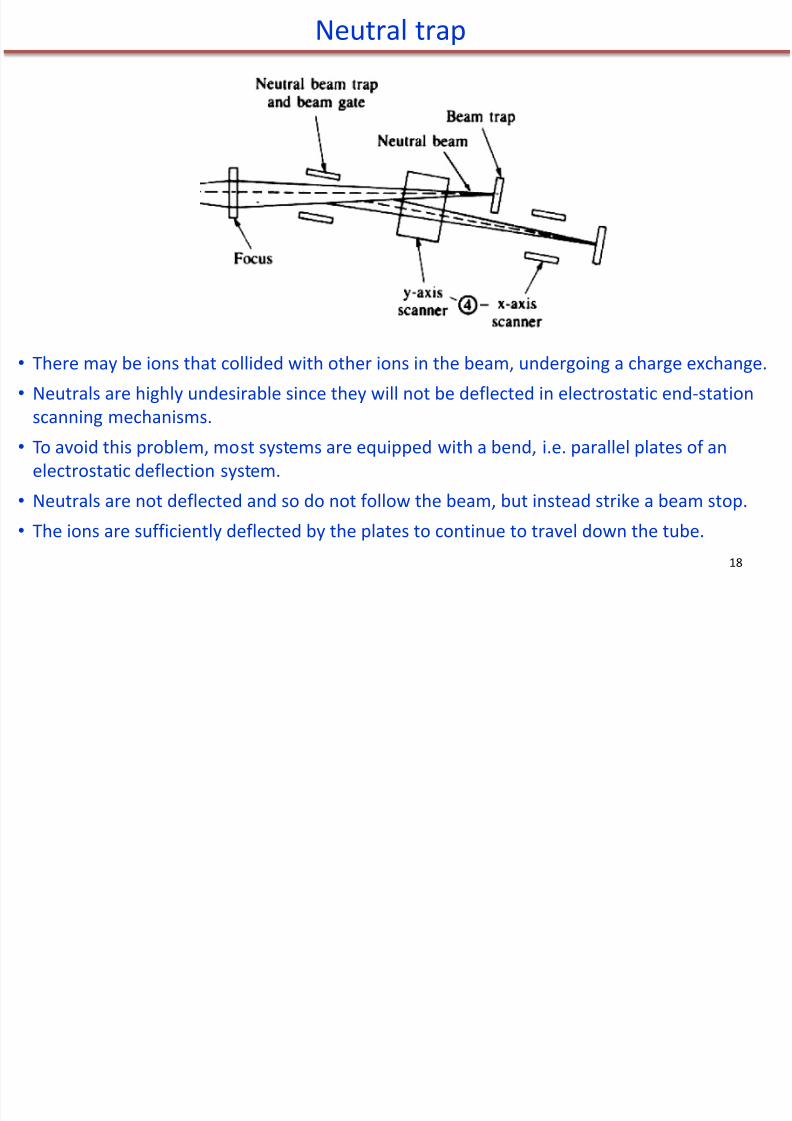
8/11/2019 Chapter 8 Ion Implantation _ I (3)
http://slidepdf.com/reader/full/chapter-8-ion-implantation-i-3 19/40
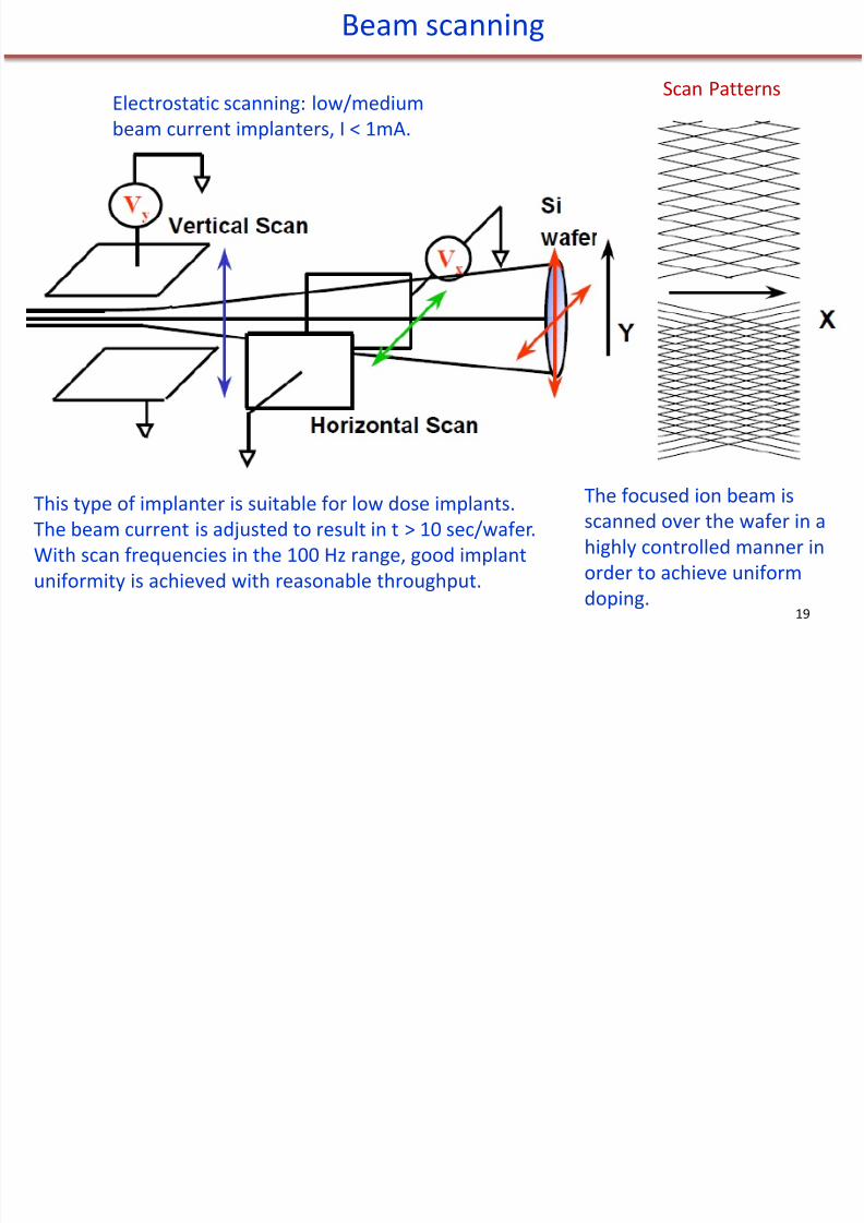
Electrostatic scanning: low/mediumbeam current implanters, I < 1mA.
This type of implanter is suitable for low dose implants.The beam current is adjusted to result in t > 10 sec/wafer.With scan frequencies in the 100 Hz range, good implantuniformity is achieved with reasonable throughput.
Scan Patterns
Beam scanning
The focused ion beam isscanned over the wafer in ahighly controlled manner inorder to achieve uniform
doping. 19
8/11/2019 Chapter 8 Ion Implantation _ I (3)
http://slidepdf.com/reader/full/chapter-8-ion-implantation-i-3 20/40
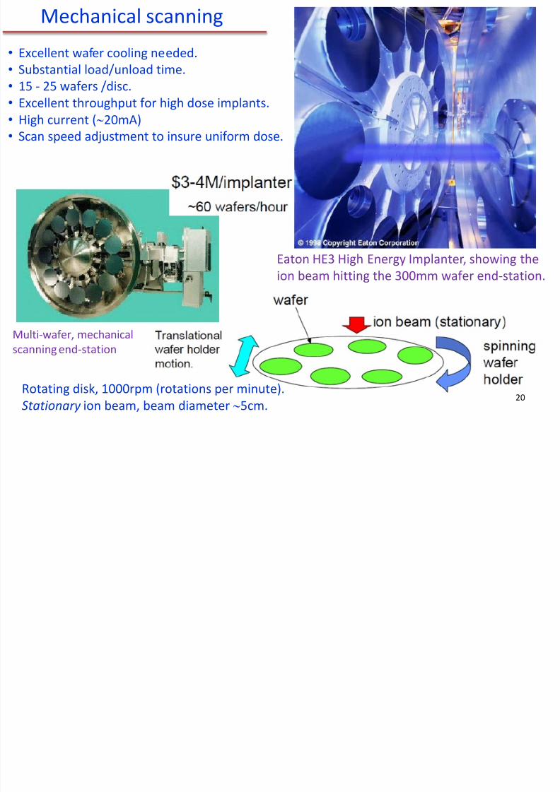
• Excellent wafer cooling needed.• Substantial load/unload time.• 15 - 25 wafers /disc.• Excellent throughput for high dose implants.• High current ( 20mA)• Scan speed adjustment to insure uniform dose.
Mechanical scanning
Multi-wafer, mechanicalscanning end-station
Rotating disk, 1000rpm (rotations per minute).Stationary ion beam, beam diameter 5cm.
Eaton HE3 High Energy Implanter, showing theion beam hitting the 300mm wafer end-station.
20
8/11/2019 Chapter 8 Ion Implantation _ I (3)
http://slidepdf.com/reader/full/chapter-8-ion-implantation-i-3 21/40
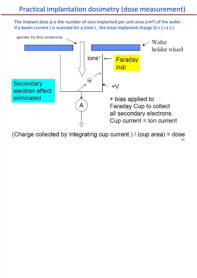
Practical implantation dosimetry (dose measurement)
The implant dose is the number of ions implanted per unit area (cm 2) of the wafer.If a beam current I is scanned for a time t , the total implanted charge Q = ( I x t ).
21
8/11/2019 Chapter 8 Ion Implantation _ I (3)
http://slidepdf.com/reader/full/chapter-8-ion-implantation-i-3 22/40
1. Introduction and application.
2. Ion implantation tools.
3. Dopant distribution profile.
4. Mask thickness and lateral distribution.
5. Effect of channeling.
6. Damage caused by ion implantation.
7. Damage repair.
Chapter 8 Ion implantation
NE 343: Microfabrication and Thin Film TechnologyInstructor: Bo Cui, ECE, University of Waterloo, [email protected]: Silicon VLSI Technology by Plummer, Deal, Griffin
22
8/11/2019 Chapter 8 Ion Implantation _ I (3)
http://slidepdf.com/reader/full/chapter-8-ion-implantation-i-3 23/40
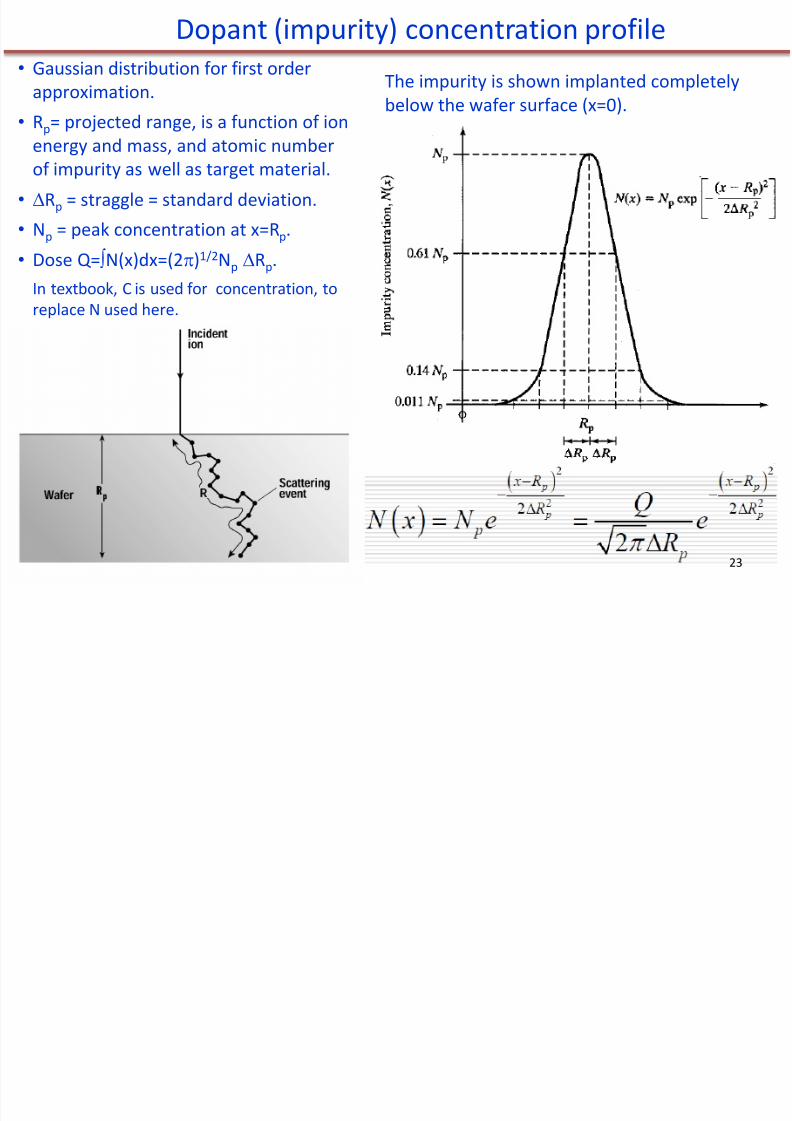
• Gaussian distribution for first orderapproximation.
• Rp= projected range, is a function of ionenergy and mass, and atomic numberof impurity as well as target material.
• Rp = straggle = standard deviation.• Np = peak concentration at x=R p.• Dose Q= N(x)dx=(2 )1/2 Np Rp.
In textbook, C is used for concentration, toreplace N used here.
Dopant (impurity) concentration profile
The impurity is shown implanted completelybelow the wafer surface (x=0).
23
8/11/2019 Chapter 8 Ion Implantation _ I (3)
http://slidepdf.com/reader/full/chapter-8-ion-implantation-i-3 24/40
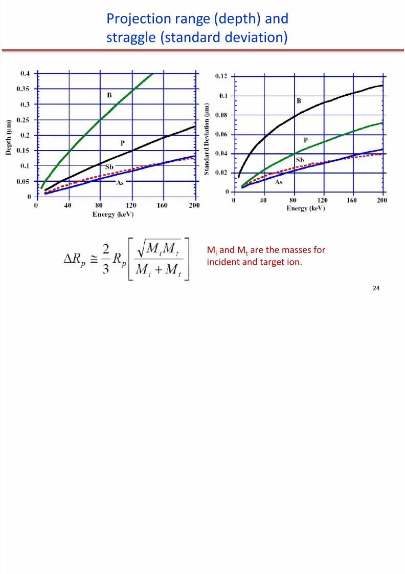
Projection range (depth) andstraggle (standard deviation)
Mi and M t are the masses forincident and target ion.
24

8/11/2019 Chapter 8 Ion Implantation _ I (3)
http://slidepdf.com/reader/full/chapter-8-ion-implantation-i-3 25/40
Example
25
8/11/2019 Chapter 8 Ion Implantation _ I (3)
http://slidepdf.com/reader/full/chapter-8-ion-implantation-i-3 26/40
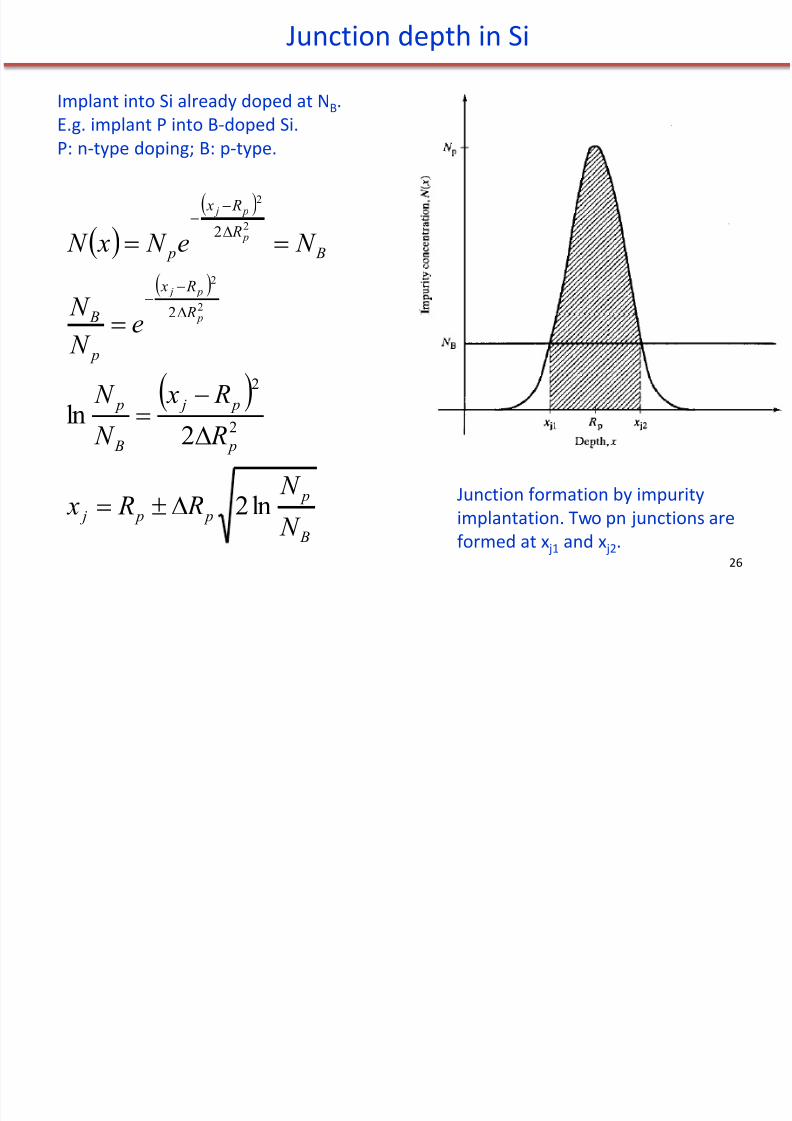
Junction depth in Si
Junction formation by impurityimplantation. Two pn junctions areformed at x j1 and x j2.
B
p p p j
p
p j
B
p
R
R x
p
B
B R
R x
p
N
N R R x
R
R x
N
N
e N N
N e N x N
p
p j
p
p j
ln2
2ln 2
2
2
2
2
2
2
2
Implant into Si already doped at N B.E.g. implant P into B-doped Si.P: n-type doping; B: p-type.
26

8/11/2019 Chapter 8 Ion Implantation _ I (3)
http://slidepdf.com/reader/full/chapter-8-ion-implantation-i-3 27/40
Example calculations
27
8/11/2019 Chapter 8 Ion Implantation _ I (3)
http://slidepdf.com/reader/full/chapter-8-ion-implantation-i-3 28/40
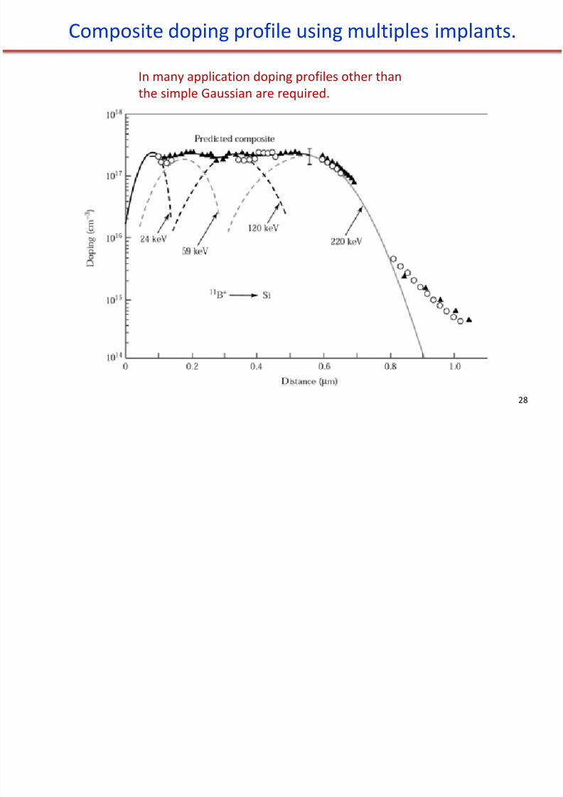
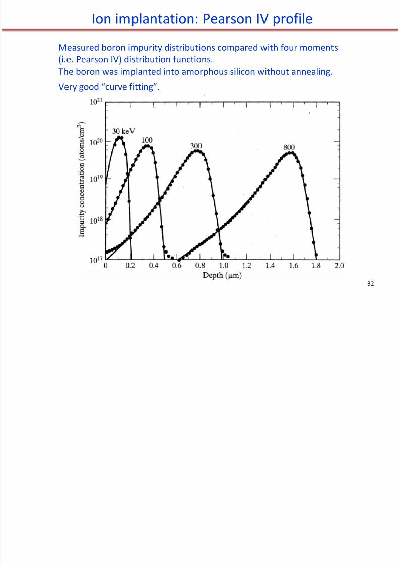
In many application doping profiles other thanthe simple Gaussian are required.
Composite doping profile using multiples implants.
28
8/11/2019 Chapter 8 Ion Implantation _ I (3)
http://slidepdf.com/reader/full/chapter-8-ion-implantation-i-3 29/40
8/11/2019 Chapter 8 Ion Implantation _ I (3)
http://slidepdf.com/reader/full/chapter-8-ion-implantation-i-3 30/40
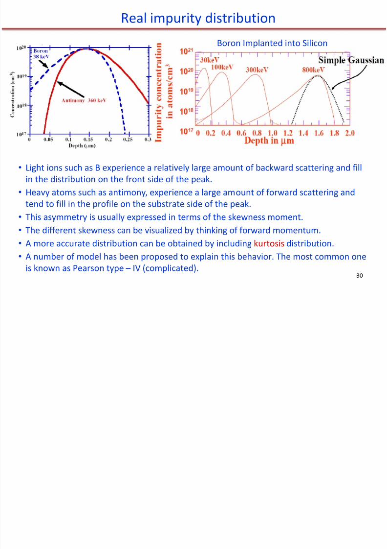
• Light ions such as B experience a relatively large amount of backward scattering and fillin the distribution on the front side of the peak.
• Heavy atoms such as antimony, experience a large amount of forward scattering and
tend to fill in the profile on the substrate side of the peak.• This asymmetry is usually expressed in terms of the skewness moment.• The different skewness can be visualized by thinking of forward momentum.• A more accurate distribution can be obtained by including kurtosis distribution.• A number of model has been proposed to explain this behavior. The most common one
is known as Pearson type – IV (complicated).
Real impurity distribution
Boron Implanted into Silicon
30
Moments description

8/11/2019 Chapter 8 Ion Implantation _ I (3)
http://slidepdf.com/reader/full/chapter-8-ion-implantation-i-3 31/40
Moments description
31
8/11/2019 Chapter 8 Ion Implantation _ I (3)
http://slidepdf.com/reader/full/chapter-8-ion-implantation-i-3 32/40
8/11/2019 Chapter 8 Ion Implantation _ I (3)
http://slidepdf.com/reader/full/chapter-8-ion-implantation-i-3 33/40
1. Introduction and application.
2. Ion implantation tools.
3. Dopant distribution profile.
4. Mask thickness and lateral distribution.
5. Effect of channeling.
6. Damage caused by ion implantation.
7. Damage repair.
Chapter 8 Ion implantation
NE 343: Microfabrication and Thin Film Technology
Instructor: Bo Cui, ECE, University of Waterloo, [email protected]: Silicon VLSI Technology by Plummer, Deal, Griffin
33
8/11/2019 Chapter 8 Ion Implantation _ I (3)
http://slidepdf.com/reader/full/chapter-8-ion-implantation-i-3 34/40
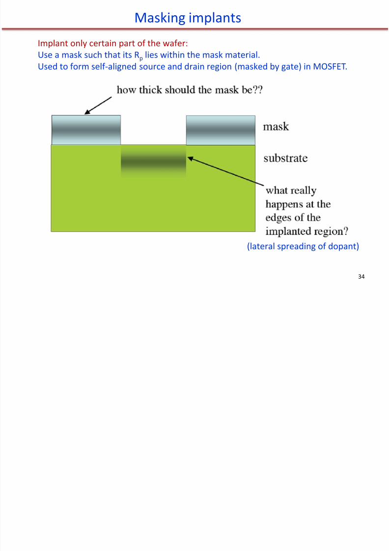
Masking implants
Implant only certain part of the wafer:Use a mask such that its R p lies within the mask material.
Used to form self-aligned source and drain region (masked by gate) in MOSFET.
(lateral spreading of dopant)
34
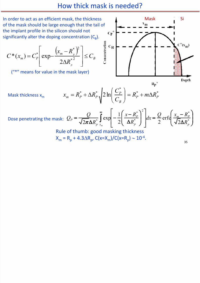
How thick mask is needed?
8/11/2019 Chapter 8 Ion Implantation _ I (3)
http://slidepdf.com/reader/full/chapter-8-ion-implantation-i-3 35/40
***
** ln2 P P B
P P P m Rm R
C C
R R x
Mask SiIn order to act as an efficient mask, the thicknessof the mask should be large enough that the tail ofthe implant profile in the silicon should not
significantly alter the doping concentration (C B).
How thick mask is needed?
B
m P m C
R
R xC xC
P
P
2*
2**
2exp)(*
(“*” means for value in the mask layer)
*
*2
*
*
* 2erfc
221
exp2 p
P m
x p
P
p P
R R xQ
dx R R x
RQ
Qm
Mask thickness x m
Dose penetrating the mask:
Rule of thumb: good masking thicknessX
m = R
p + 4.3 R
p, C(x=X
m)/C(x=R
p) 10 -4.
35

8/11/2019 Chapter 8 Ion Implantation _ I (3)
http://slidepdf.com/reader/full/chapter-8-ion-implantation-i-3 36/40
36
Mask material: resist
8/11/2019 Chapter 8 Ion Implantation _ I (3)
http://slidepdf.com/reader/full/chapter-8-ion-implantation-i-3 37/40
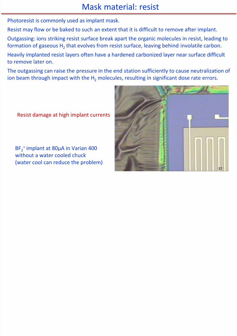
Photoresist is commonly used as implant mask.
Resist may flow or be baked to such an extent that it is difficult to remove after implant.
Outgassing: ions striking resist surface break apart the organic molecules in resist, leading toformation of gaseous H 2 that evolves from resist surface, leaving behind involatile carbon.
Heavily implanted resist layers often have a hardened carbonized layer near surface difficultto remove later on.
The outgassing can raise the pressure in the end station sufficiently to cause neutralization ofion beam through impact with the H 2 molecules, resulting in significant dose rate errors.
Mask material: resist
Resist damage at high implant currents
BF2+ implant at 80μA in Varian 400
without a water cooled chuck(water cool can reduce the problem)
37
8/11/2019 Chapter 8 Ion Implantation _ I (3)
http://slidepdf.com/reader/full/chapter-8-ion-implantation-i-3 38/40
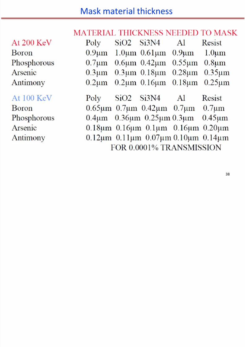
Mask material thickness
38
l
8/11/2019 Chapter 8 Ion Implantation _ I (3)
http://slidepdf.com/reader/full/chapter-8-ion-implantation-i-3 39/40
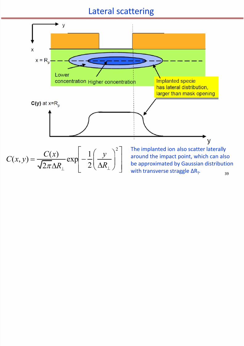
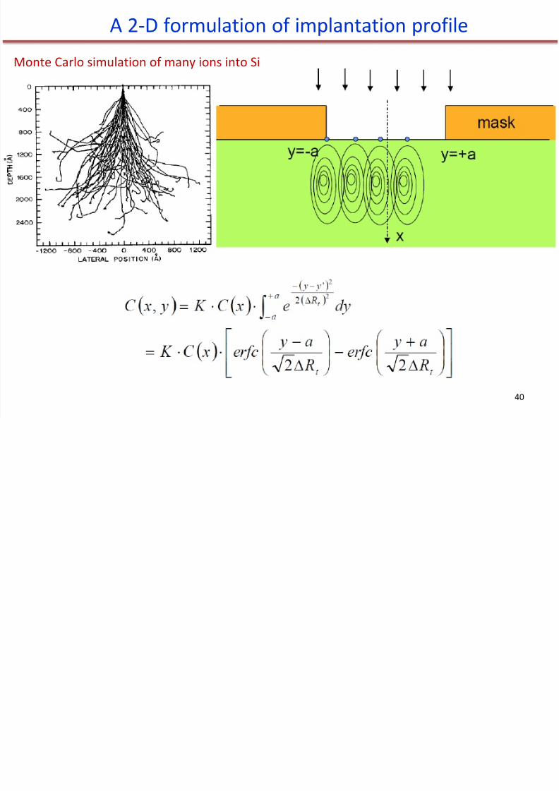
Lateral scattering
2
21
exp2
)(),(
R y
R xC
y xC
The implanted ion also scatter laterallyaround the impact point, which can alsobe approximated by Gaussian distribution
with transverse straggle ΔRT. 39
f l f l f l
8/11/2019 Chapter 8 Ion Implantation _ I (3)
http://slidepdf.com/reader/full/chapter-8-ion-implantation-i-3 40/40
A 2-D formulation of implantation profile
Monte Carlo simulation of many ions into Si