Embed Size (px)
Citation preview
CHAPTER
4Solidification
and Crystalline Imperfections
in Solids
4-1
Copyright © The McGraw-Hill Companies, Inc. Permission required for reproduction or display
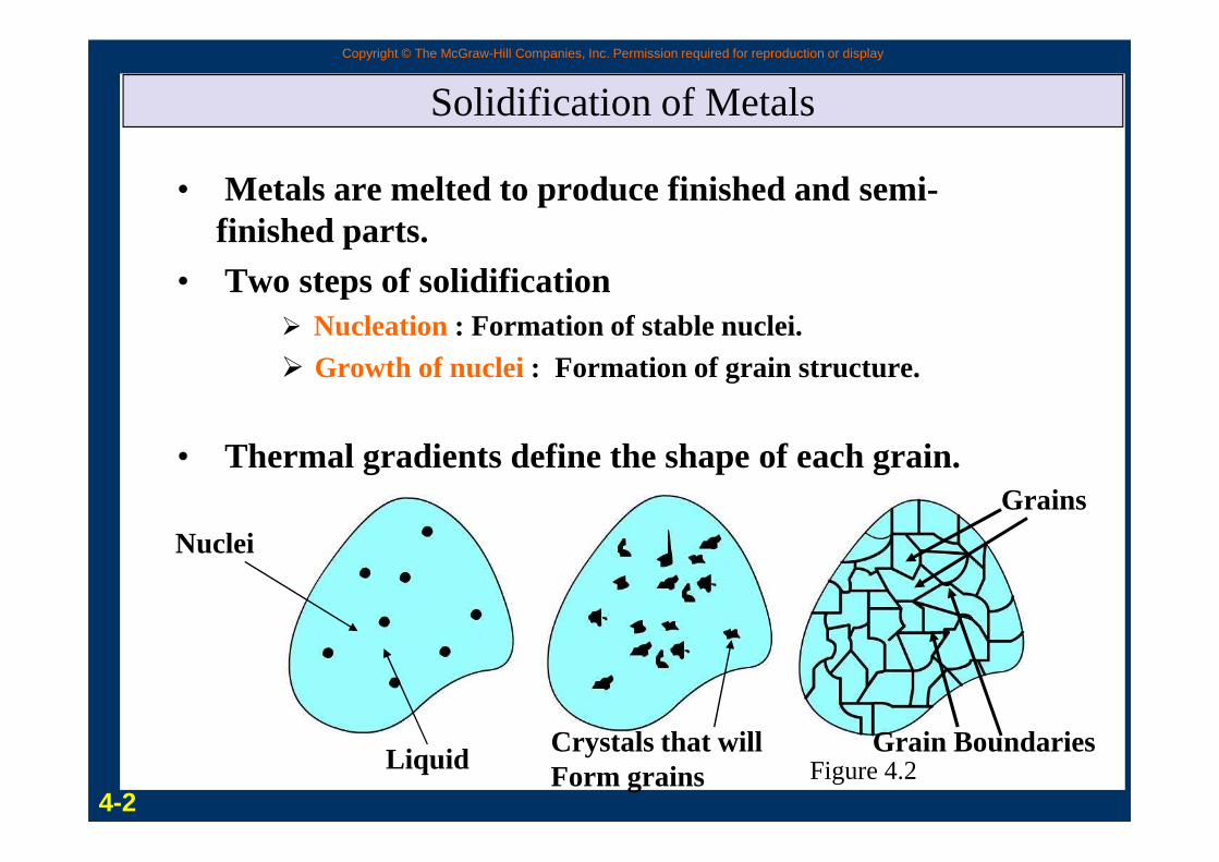
Solidification of Metals
• Metals are melted to produce finished and semi-finished parts.
• Two steps of solidification � Nucleation : Formation of stable nuclei. � Growth of nuclei : Formation of grain structure.
• Thermal gradients define the shape of each grain.
Liquid
Nuclei
Crystals that willForm grains
Grain Boundaries
Grains
4-2Figure 4.2
Copyright © The McGraw-Hill Companies, Inc. Permission required for reproduction or display
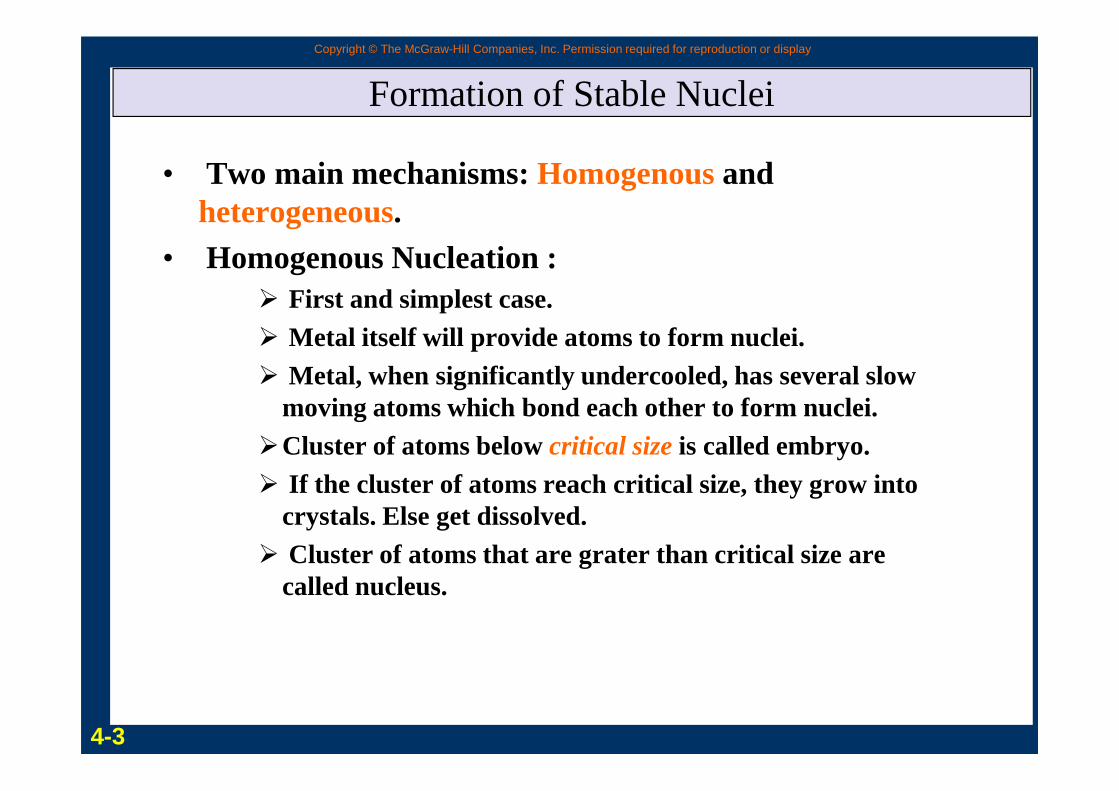
Formation of Stable Nuclei
• Two main mechanisms: Homogenousand heterogeneous.
• Homogenous Nucleation :� First and simplest case.� Metal itself will provide atoms to form nuclei.� Metal, when significantly undercooled, has several slow
moving atoms which bond each other to form nuclei. moving atoms which bond each other to form nuclei. �Cluster of atoms below critical size is called embryo.� If the cluster of atoms reach critical size, they grow into
crystals. Else get dissolved.� Cluster of atoms that are grater than critical size are
called nucleus.
4-3
Copyright © The McGraw-Hill Companies, Inc. Permission required for reproduction or display
Energies involved in homogenous nucleation.
Volume free energy Gv
• Released by liquid to solid transformation.
• ∆Gv is change in free energy per unit volume between liquid and solid.
Surface energy Gs
• Required to form new solid surface
• ∆Gs is energy needed to create a surface.
• γ is specific surface free γ liquid and solid.
• free energy change for a spherical nucleus of radius r is given by
• γ is specific surface free energy.
Then
• ∆Gs is retarding energy.
γπ 2s 4G r=∆
vGrr ∆= 3
3
4π
4-4
Copyright © The McGraw-Hill Companies, Inc. Permission required for reproduction or display
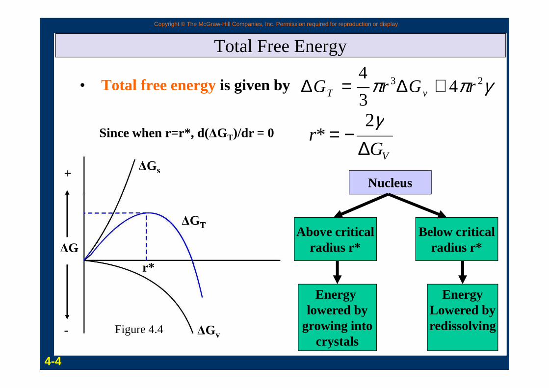
Total Free Energy
• Total free energyis given by γππ 23 43
4rGrG vT +∆=∆
Nucleus
VGr
∆−=
γ2*Since when r=r*, d(∆GT)/dr = 0
+∆Gs
Above criticalradius r*
Below criticalradius r*
Energy lowered by
growing intocrystals
EnergyLowered byredissolving
r*r
∆G
- ∆Gv
∆GT
4-4
r*
Figure 4.4
Copyright © The McGraw-Hill Companies, Inc. Permission required for reproduction or display
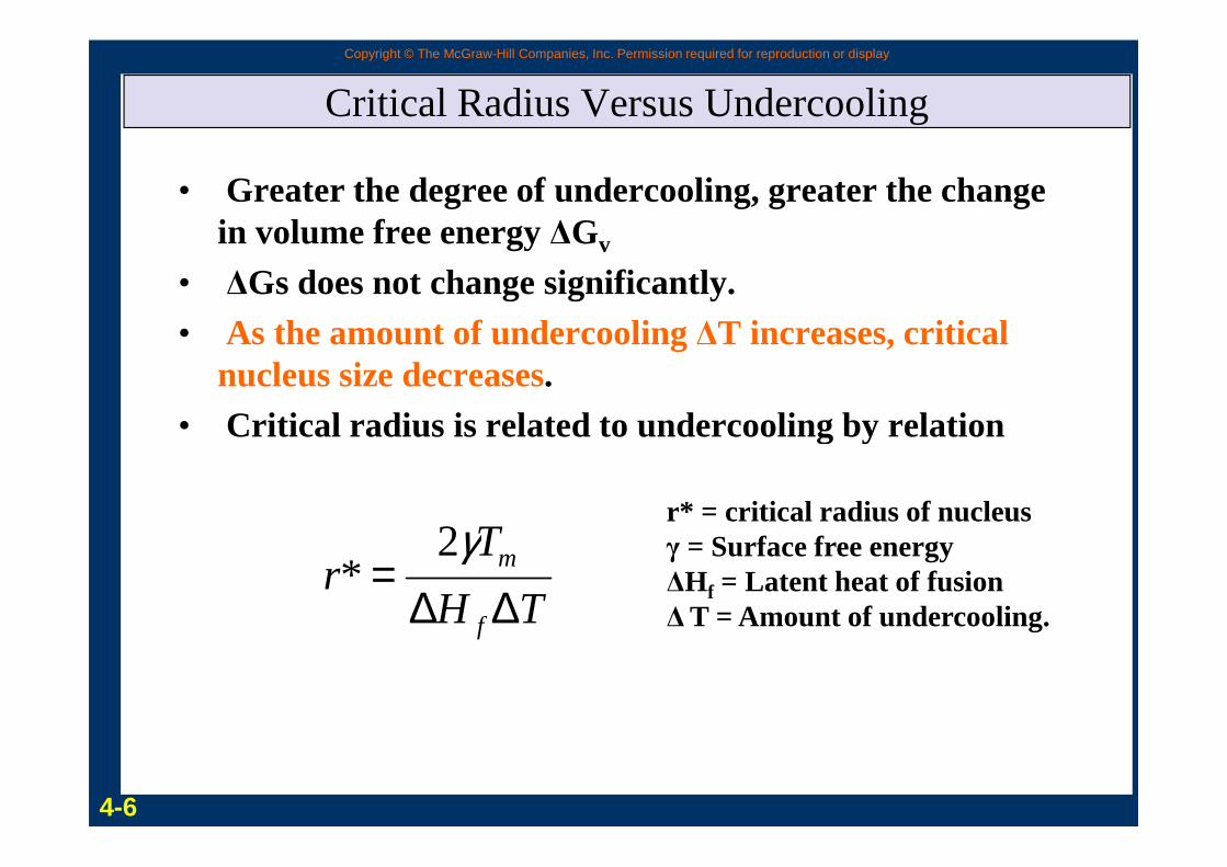
Critical Radius Versus Undercooling
• Greater the degree of undercooling, greater the change in volume free energy ∆Gv
• ∆Gs does not change significantly.• As the amount of undercooling ∆T increases, critical
nucleus size decreases.• Critical radius is related to undercooling by relation • Critical radius is related to undercooling by relation
TH
Tr
f
m
∆∆=
γ2*
r* = critical radius of nucleusγ = Surface free energy∆H f = Latent heat of fusion∆ T = Amount of undercooling.
4-6
Copyright © The McGraw-Hill Companies, Inc. Permission required for reproduction or display
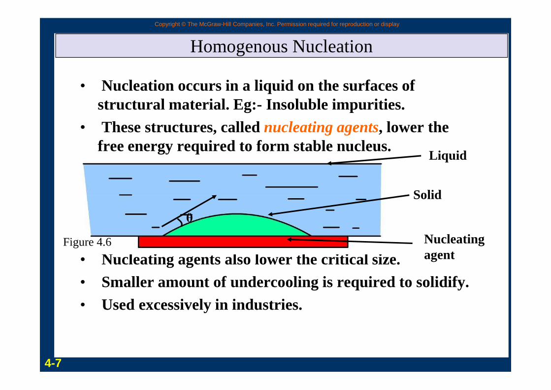
Homogenous Nucleation
• Nucleation occurs in a liquid on the surfaces of structural material. Eg:- Insoluble impurities.
• These structures, called nucleating agents, lower the free energy required to form stable nucleus.
Liquid
Solid
• Nucleating agents also lower the critical size.• Smaller amount of undercooling is required to solidify.• Used excessively in industries.
Solid
Nucleating agent
θ
4-7
Figure 4.6
Copyright © The McGraw-Hill Companies, Inc. Permission required for reproduction or display
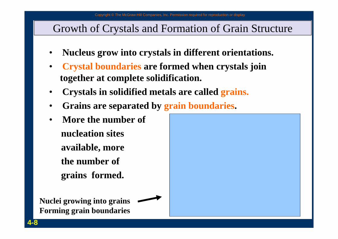
Growth of Crystals and Formation of Grain Structure
• Nucleus grow into crystals in different orientations.• Crystal boundariesare formed when crystals join
together at complete solidification. • Crystals in solidified metals are called grains.• Grains are separated by grain boundaries.• More the number of • More the number of
nucleation sites available, more the number of grains formed.
Nuclei growing into grainsForming grain boundaries
4-8
Copyright © The McGraw-Hill Companies, Inc. Permission required for reproduction or display
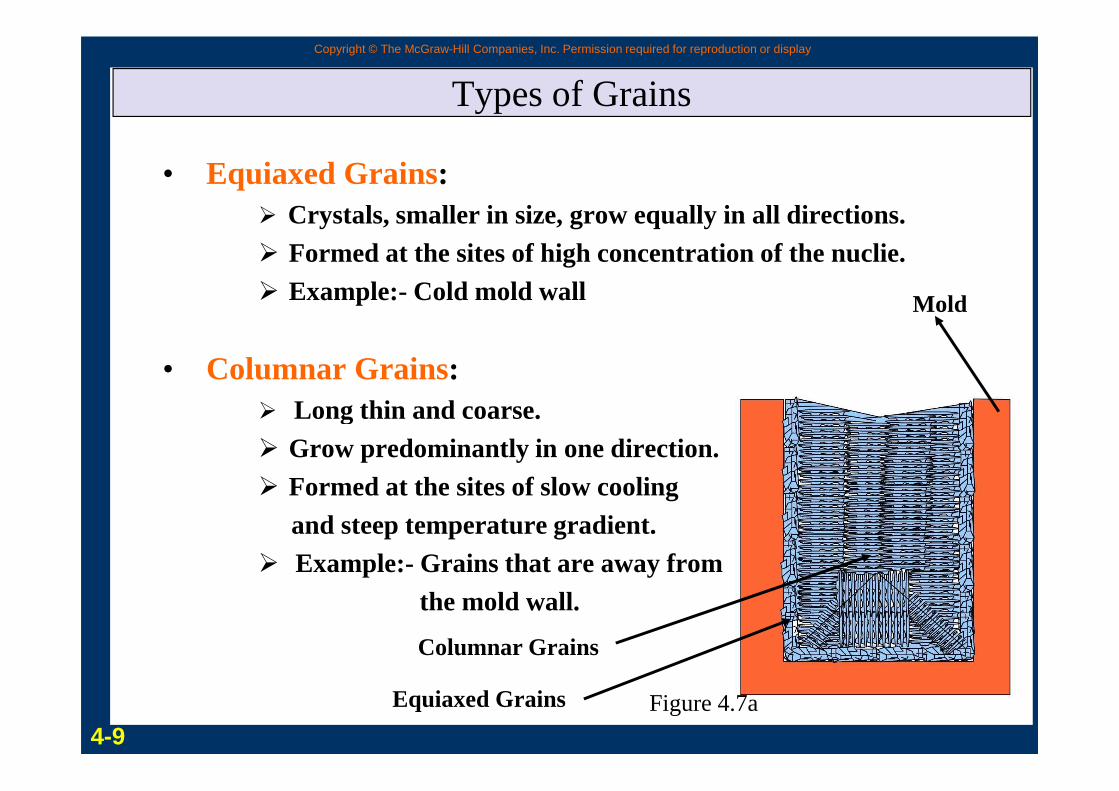
Types of Grains
• Equiaxed Grains: � Crystals, smaller in size, grow equally in all directions.� Formed at the sites of high concentration of the nuclie.� Example:- Cold mold wall
• Columnar Grains: Long thin and coarse.
Mold
� Long thin and coarse.� Grow predominantly in one direction.� Formed at the sites of slow cooling
and steep temperature gradient.� Example:- Grains that are away from
the mold wall.
Columnar Grains
Equiaxed Grains
4-9Figure 4.7a
Copyright © The McGraw-Hill Companies, Inc. Permission required for reproduction or display
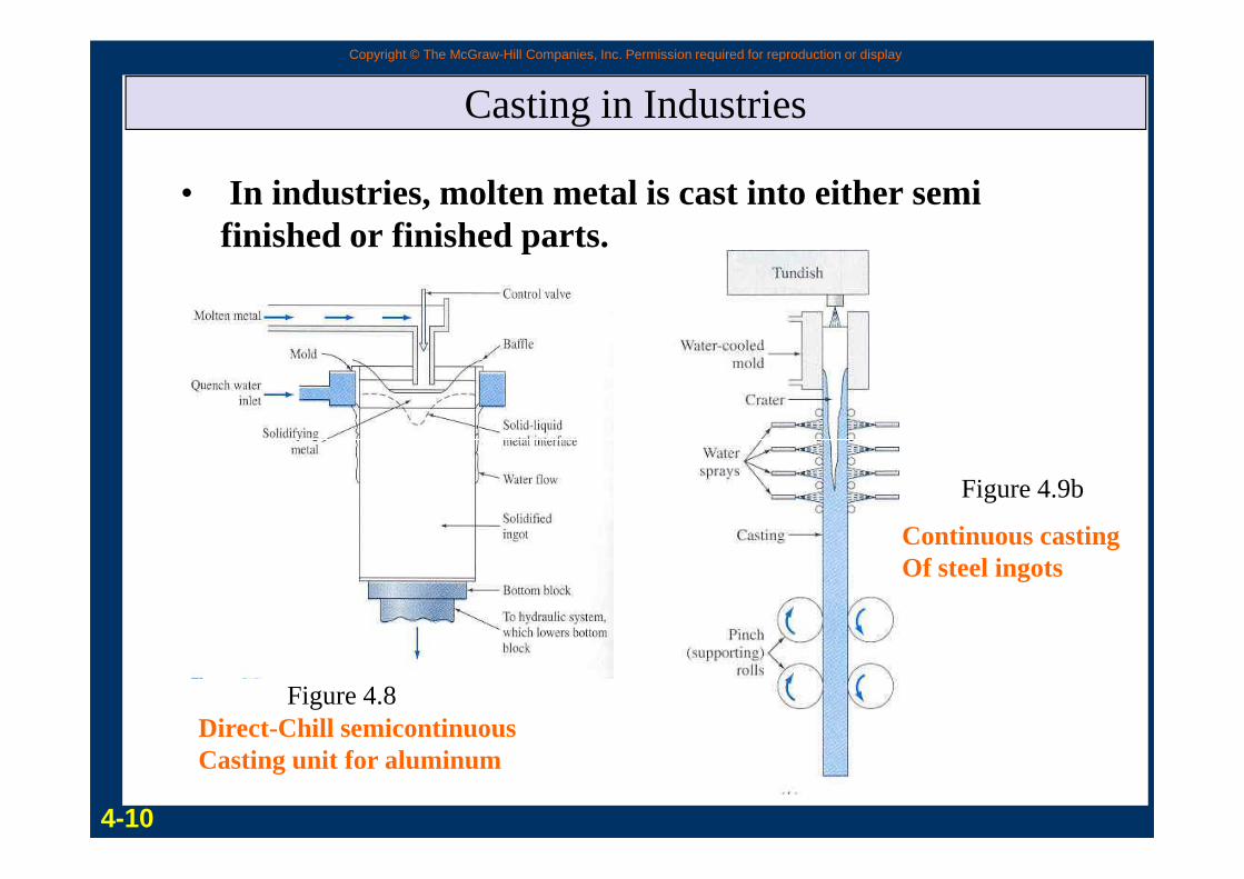
Casting in Industries
• In industries, molten metal is cast into either semi finished or finished parts.
4-10
Figure 4.8Direct-Chill semicontinuousCasting unit for aluminum
Figure 4.9b
Continuous castingOf steel ingots
Copyright © The McGraw-Hill Companies, Inc. Permission required for reproduction or display
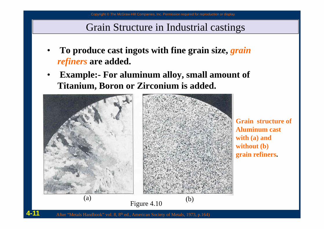
Grain Structure in Industrial castings
• To produce cast ingots with fine grain size, grain refiners are added.
• Example:- For aluminum alloy, small amount of Titanium, Boron or Zirconium is added.
4-11Figure 4.10
(a) (b)
Grain structure ofAluminum cast with (a) and without (b)grain refiners.
After “Metals Handbook” vol. 8, 8th ed., American Society of Metals, 1973, p.164)
Copyright © The McGraw-Hill Companies, Inc. Permission required for reproduction or display
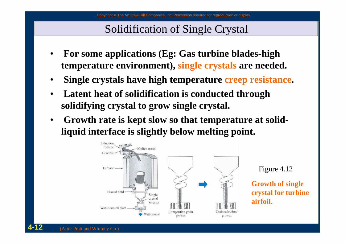
Solidification of Single Crystal
• For some applications (Eg: Gas turbine blades-high temperature environment), single crystalsare needed.
• Single crystals have high temperature creep resistance. • Latent heat of solidification is conducted through
solidifying crystal to grow single crystal.• Growth rate is kept slow so that temperature at solid-• Growth rate is kept slow so that temperature at solid-
liquid interface is slightly below melting point.
4-12
Figure 4.12
Growth of singlecrystal for turbineairfoil.
(After Pratt and Whitney Co.)
Copyright © The McGraw-Hill Companies, Inc. Permission required for reproduction or display
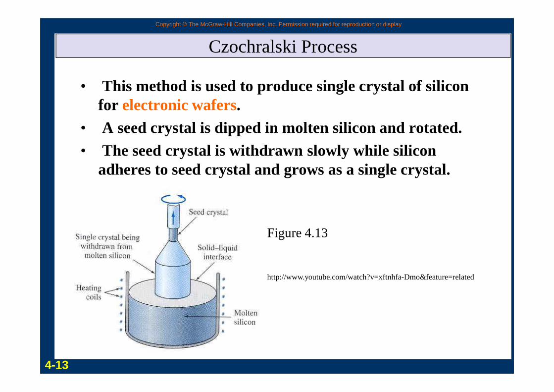
Czochralski Process
• This method is used to produce single crystal of silicon for electronic wafers.
• A seed crystal is dipped in molten silicon and rotated.• The seed crystal is withdrawn slowly while silicon
adheres to seed crystal and grows as a single crystal.
4-13
Figure 4.13
http://www.youtube.com/watch?v=xftnhfa-Dmo&feature=related
Copyright © The McGraw-Hill Companies, Inc. Permission required for reproduction or display
Metallic Solid Solutions
• Alloys are used in most engineering applications.• Alloy is an mixture of two or more metals and
nonmetals.• Example:
� Cartridge brass is binary alloy of 70% Cu and 30% Zinc. � Iconel is a nickel based superalloy with about 10 elements.� Iconel is a nickel based superalloy with about 10 elements.
• Solid solution is a simple type of alloy in which elements are dispersed in a single phase.
4-14
Copyright © The McGraw-Hill Companies, Inc. Permission required for reproduction or display
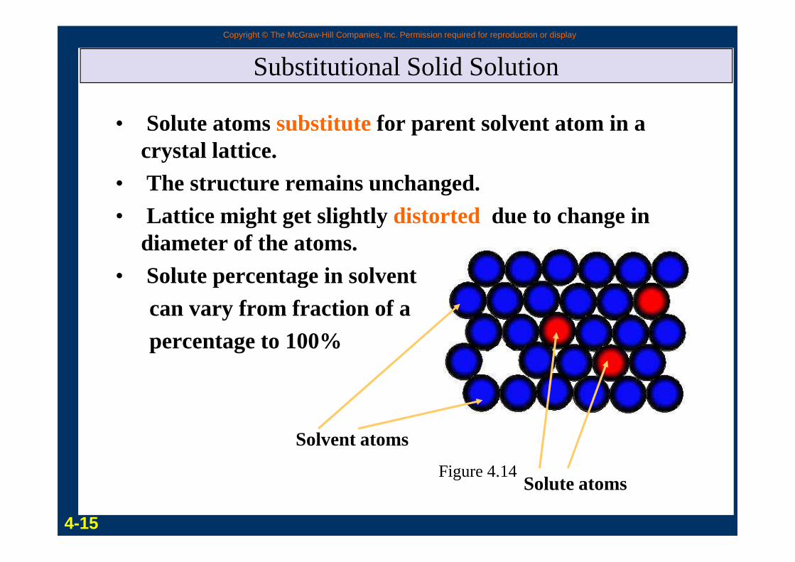
Substitutional Solid Solution
• Solute atoms substitute for parent solvent atom in a crystal lattice.
• The structure remains unchanged.• Lattice might get slightly distorted due to change in
diameter of the atoms. • Solute percentage in solvent • Solute percentage in solvent
can vary from fraction of a percentage to 100%
Solvent atoms
Solute atoms
4-15
Figure 4.14
Copyright © The McGraw-Hill Companies, Inc. Permission required for reproduction or display
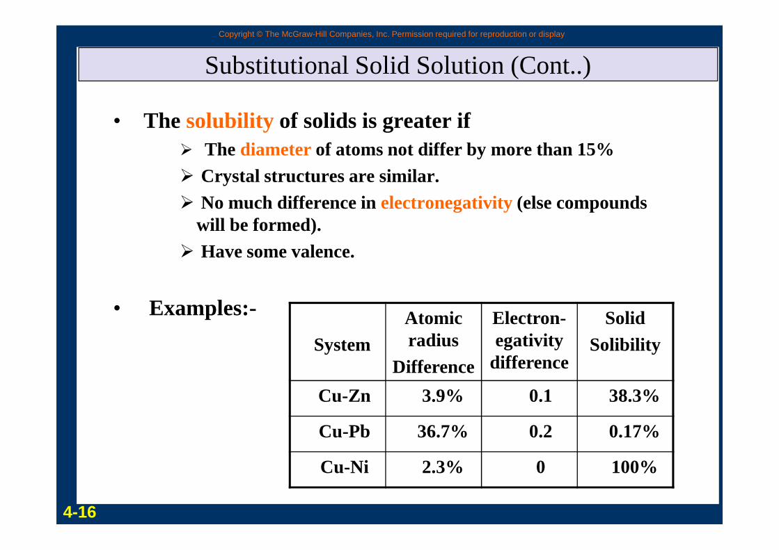
Substitutional Solid Solution (Cont..)
• The solubility of solids is greater if � The diameter of atoms not differ by more than 15% � Crystal structures are similar. � No much difference in electronegativity (else compounds
will be formed). � Have some valence.
• Examples:-
SystemAtomic radius
Difference
Electron-egativity
difference
SolidSolibility
Cu-Zn 3.9% 0.1 38.3%
Cu-Pb 36.7% 0.2 0.17%
Cu-Ni 2.3% 0 100%
4-16
Copyright © The McGraw-Hill Companies, Inc. Permission required for reproduction or display
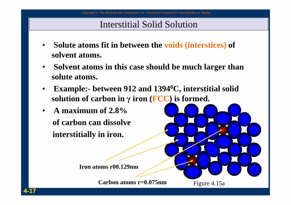
Interstitial Solid Solution
• Solute atoms fit in between the voids (interstices)of solvent atoms.
• Solvent atoms in this case should be much larger than solute atoms.
• Example:- between 912 and 13940C, interstitial solid solution of carbon in γ iron (FCC) is formed. solution of carbon in γ iron (FCC) is formed.
• A maximum of 2.8% of carbon can dissolve interstitially in iron.
Carbon atoms r=0.075nm
Iron atoms r00.129nm
4-17Figure 4.15a
Copyright © The McGraw-Hill Companies, Inc. Permission required for reproduction or display
Crystalline Imperfections
• No crystal is perfect.• Imperfections affect mechanical
properties, chemical properties and electrical properties.
• Imperfections can be classified as � Zero dimension point deffects.� Zero dimension point deffects.� One dimension / line deffects (dislocations). � Two dimension deffects.� Three dimension deffects (cracks).
4-18
Copyright © The McGraw-Hill Companies, Inc. Permission required for reproduction or display
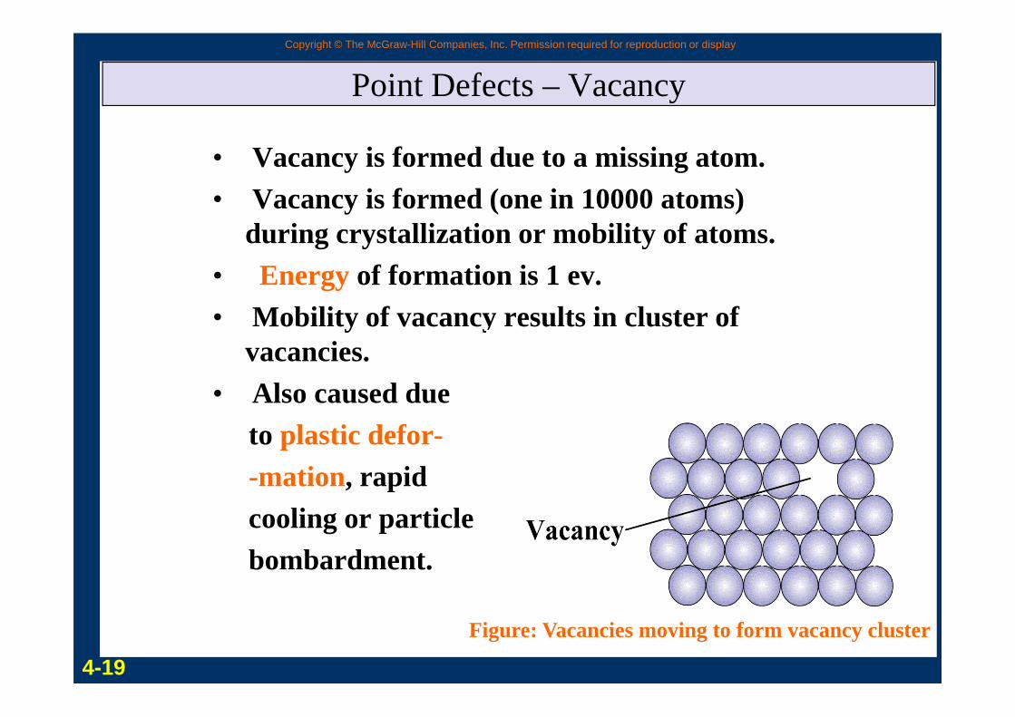
Point Defects – Vacancy
• Vacancy is formed due to a missing atom.• Vacancy is formed (one in 10000 atoms)
during crystallization or mobility of atoms. • Energy of formation is 1 ev.• Mobility of vacancy results in cluster of
vacancies.vacancies.• Also caused due
to plastic defor--mation, rapid cooling or particlebombardment.
Figure: Vacancies moving to form vacancy cluster
4-19
Copyright © The McGraw-Hill Companies, Inc. Permission required for reproduction or display
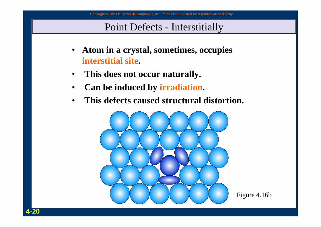
Point Defects - Interstitially
• Atom in a crystal, sometimes, occupies interstitial site.
• This does not occur naturally.• Can be induced by irradiation .• This defects caused structural distortion.
4-20
Figure 4.16b
Copyright © The McGraw-Hill Companies, Inc. Permission required for reproduction or display
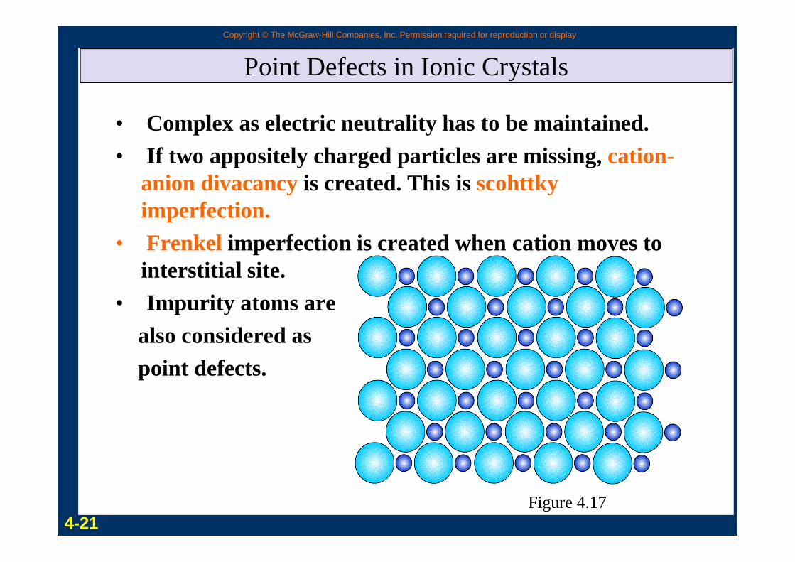
Point Defects in Ionic Crystals
• Complex as electric neutrality has to be maintained.• If two appositely charged particles are missing, cation-
anion divacancyis created. This is scohttky imperfection.
• Frenkel imperfection is created when cation moves to interstitial site. interstitial site.
• Impurity atoms are also considered as point defects.
4-21Figure 4.17
Copyright © The McGraw-Hill Companies, Inc. Permission required for reproduction or display
Line Defects – (Dislocations)
• Lattice distortions are centeredaround a line.
• Formed during� Solidification� Permanent Deformation� Vacancy condensation
• Different types of line defects are� Edge dislocation� Screw dislocation � Mixed dislocation
4-22
Copyright © The McGraw-Hill Companies, Inc. Permission required for reproduction or display
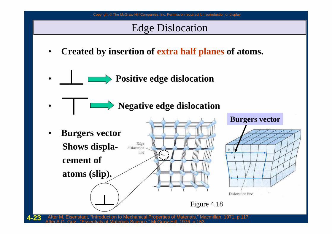
Edge Dislocation
• Created by insertion of extra half planesof atoms.
• Positive edge dislocation
• Negative edge dislocation Burgers vector
• Burgers vectorShows displa-cement of atoms (slip).
4-23
Burgers vector
Figure 4.18
After A.G. Guy , “Essentials of Materials Science,” McGraw-Hill, 1976, p.153After M. Eisenstadt, “Introduction to Mechanical Properties of Materials,” Macmillan, 1971, p.117
Copyright © The McGraw-Hill Companies, Inc. Permission required for reproduction or display
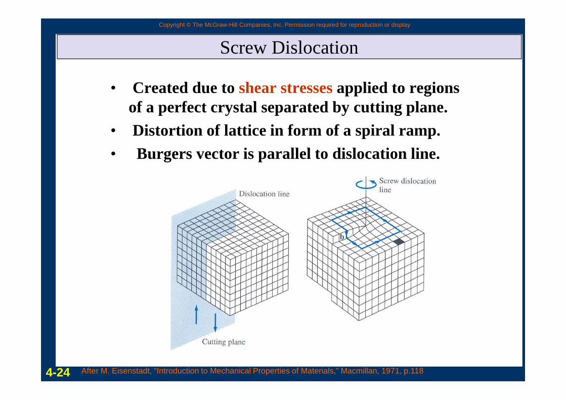
Screw Dislocation
• Created due to shear stressesapplied to regions of a perfect crystal separated by cutting plane.
• Distortion of lattice in form of a spiral ramp.• Burgers vector is parallel to dislocation line.
4-24 After M. Eisenstadt, “Introduction to Mechanical Properties of Materials,” Macmillan, 1971, p.118
Copyright © The McGraw-Hill Companies, Inc. Permission required for reproduction or display
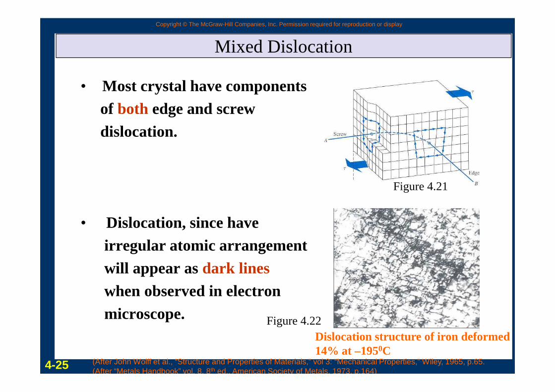
Mixed Dislocation
• Most crystal have componentsof both edge and screw dislocation.
Figure 4.21
• Dislocation, since have irregular atomic arrangementwill appear as dark lineswhen observed in electronmicroscope.
4-25 (After John Wolff et al., “Structure and Properties of Materials,” vol 3: “Mechanical Properties,” Wiley, 1965, p.65.(After “Metals Handbook” vol. 8, 8th ed., American Society of Metals, 1973, p.164)
Figure 4.22Dislocation structure of iron deformed14% at –1950C
Copyright © The McGraw-Hill Companies, Inc. Permission required for reproduction or display
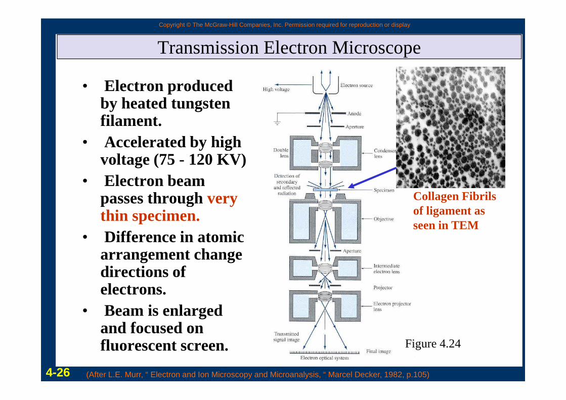
Transmission Electron Microscope
• Electron produced by heated tungsten filament.
• Accelerated by high voltage (75 - 120 KV)
• Electron beam passes through very Collagen Fibrilspasses through very thin specimen.
• Difference in atomic arrangement change directions of electrons.
• Beam is enlarged and focused on fluorescent screen.
4-26
Figure 4.24
Collagen Fibrilsof ligament asseen in TEM
(After L.E. Murr, “ Electron and Ion Microscopy and Microanalysis, “ Marcel Decker, 1982, p.105)
Copyright © The McGraw-Hill Companies, Inc. Permission required for reproduction or display
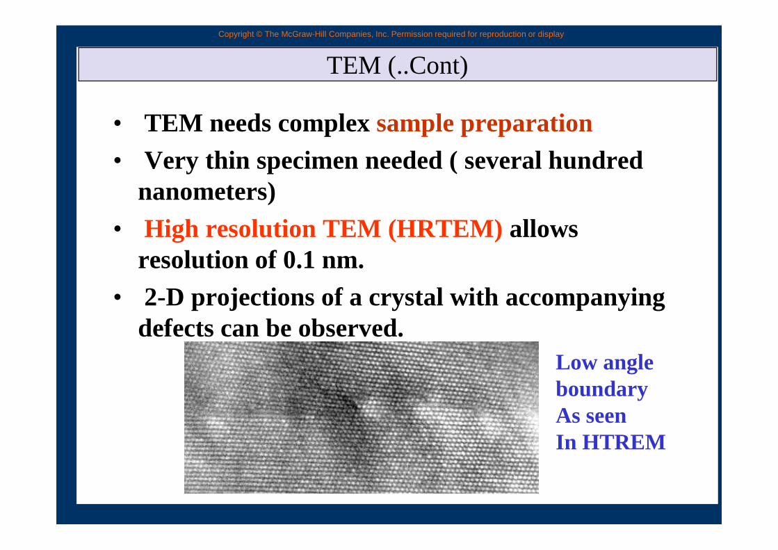
TEM (..Cont)
• TEM needs complex sample preparation
• Very thin specimen needed ( several hundred nanometers)
• High resolution TEM (HRTEM) allows resolution of 0.1 nm.
• 2-D projections of a crystal with accompanying defects can be observed.
Low angle boundaryAs seenIn HTREM
Copyright © The McGraw-Hill Companies, Inc. Permission required for reproduction or display
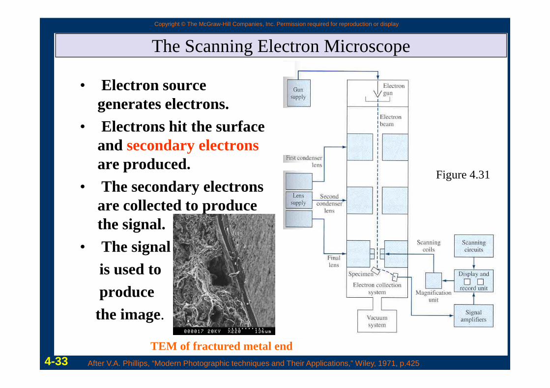
The Scanning Electron Microscope
• Electron source generates electrons.
• Electrons hit the surface and secondary electronsare produced.
• The secondary electrons Figure 4.31
• The secondary electrons are collected to produce the signal.
• The signal is used to produce the image.
TEM of fractured metal end4-33 After V.A. Phillips, “Modern Photographic techniques and Their Applications,” Wiley, 1971, p.425
Copyright © The McGraw-Hill Companies, Inc. Permission required for reproduction or display
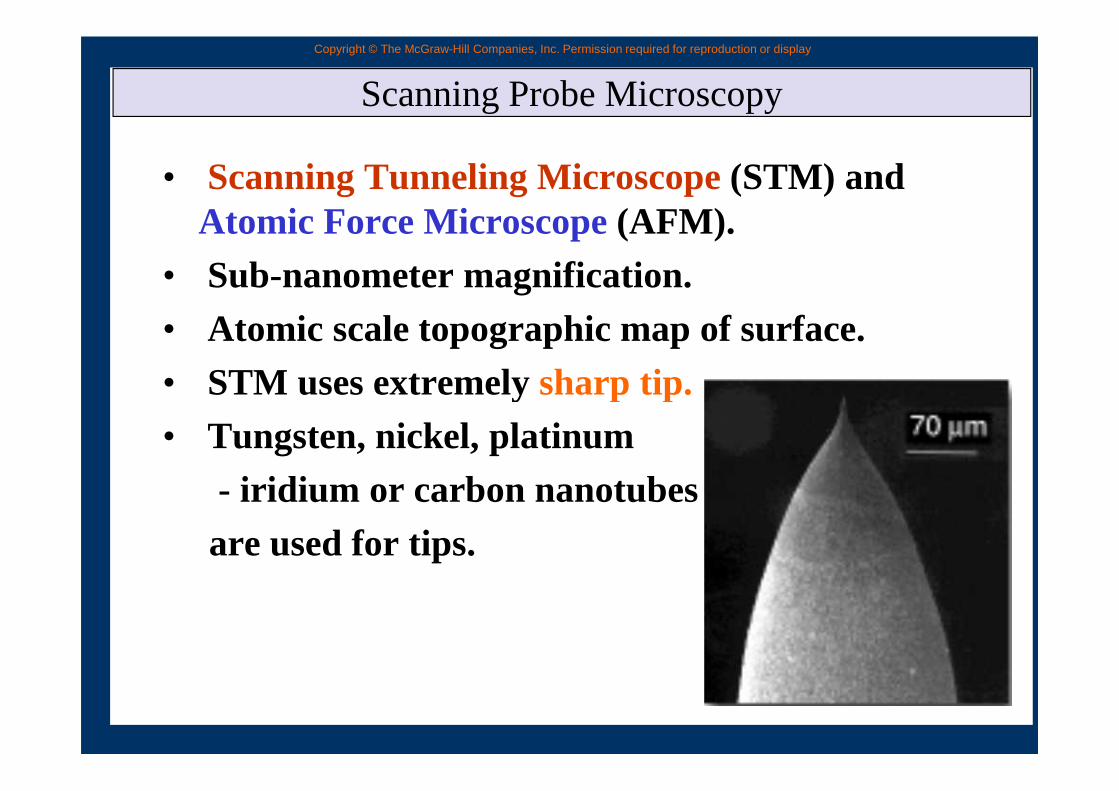
Scanning Probe Microscopy
• Scanning Tunneling Microscope(STM) and Atomic Force Microscope(AFM).
• Sub-nanometer magnification.
• Atomic scale topographic map of surface.
• STM uses extremely sharp tip.• STM uses extremely sharp tip.
• Tungsten, nickel, platinum
- iridium or carbon nanotubes
are used for tips.
Copyright © The McGraw-Hill Companies, Inc. Permission required for reproduction or display
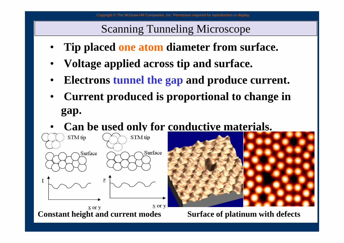
Scanning Tunneling Microscope
• Tip placed one atomdiameter from surface.
• Voltage applied across tip and surface.
• Electrons tunnel the gapand produce current.
• Current produced is proportional to change in gap.
• Can be used only for conductive materials.• Can be used only for conductive materials.
Constant height and current modes Surface of platinum with defects
Copyright © The McGraw-Hill Companies, Inc. Permission required for reproduction or display
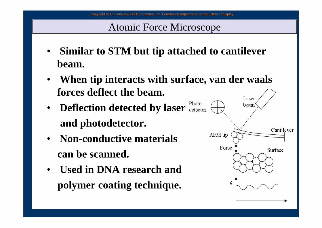
Atomic Force Microscope
• Similar to STM but tip attached to cantilever beam.
• When tip interacts with surface, van der waals forces deflect the beam.
• Deflection detected by laser
and photodetector.
• Non-conductive materials
can be scanned.
• Used in DNA research and
polymer coating technique.
Copyright © The McGraw-Hill Companies, Inc. Permission required for reproduction or display
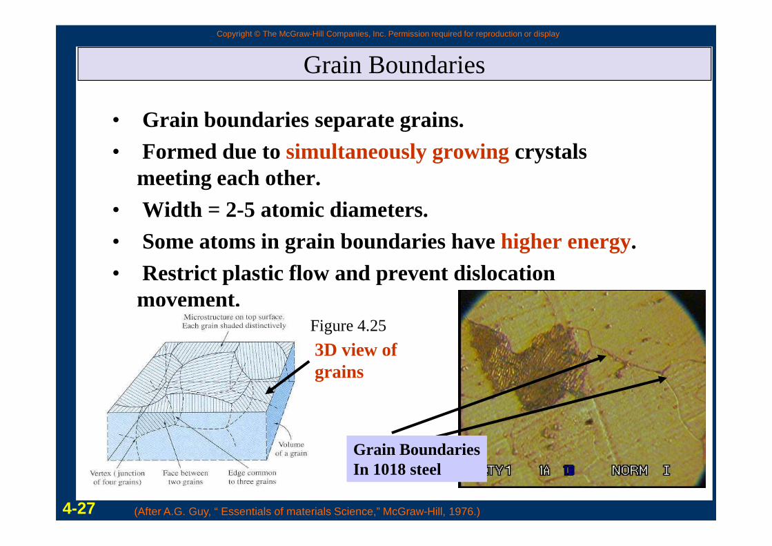
Grain Boundaries
• Grain boundaries separate grains.• Formed due to simultaneously growingcrystals
meeting each other.• Width = 2-5 atomic diameters. • Some atoms in grain boundaries have higher energy. • Restrict plastic flow and prevent dislocation • Restrict plastic flow and prevent dislocation
movement.
4-27
Figure 4.25
3D view ofgrains
Grain BoundariesIn 1018 steel
(After A.G. Guy, “ Essentials of materials Science,” McGraw-Hill, 1976.)
Copyright © The McGraw-Hill Companies, Inc. Permission required for reproduction or display
Planar Defects
• Grain boundaries, twins, low/high angle boundaries, twists and stacking faults
• Free surface is also a defect: Bonded to atoms on only one side and hence has higher state of energy Highly reactivereactive
• Nanomaterials have small clusters of atoms and hence are highly reactive.
Copyright © The McGraw-Hill Companies, Inc. Permission required for reproduction or display
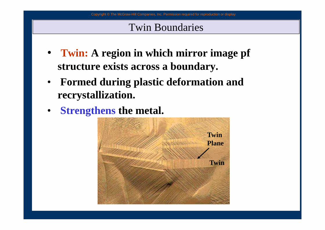
Twin Boundaries
• Twin: A region in which mirror image pf structure exists across a boundary.
• Formed during plastic deformation and recrystallization.
• Strengthensthe metal.• Strengthensthe metal.
Twin
Twin Plane
Copyright © The McGraw-Hill Companies, Inc. Permission required for reproduction or display
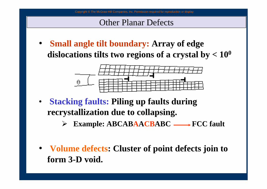
Other Planar Defects
• Small angle tilt boundary: Array of edge dislocations tilts two regions of a crystal by < 100
• Stacking faults: Piling up faults during recrystallization due to collapsing.
� Example: ABCABAACBABC FCC fault
• Volume defects: Cluster of point defects join to form 3-D void.
Copyright © The McGraw-Hill Companies, Inc. Permission required for reproduction or display
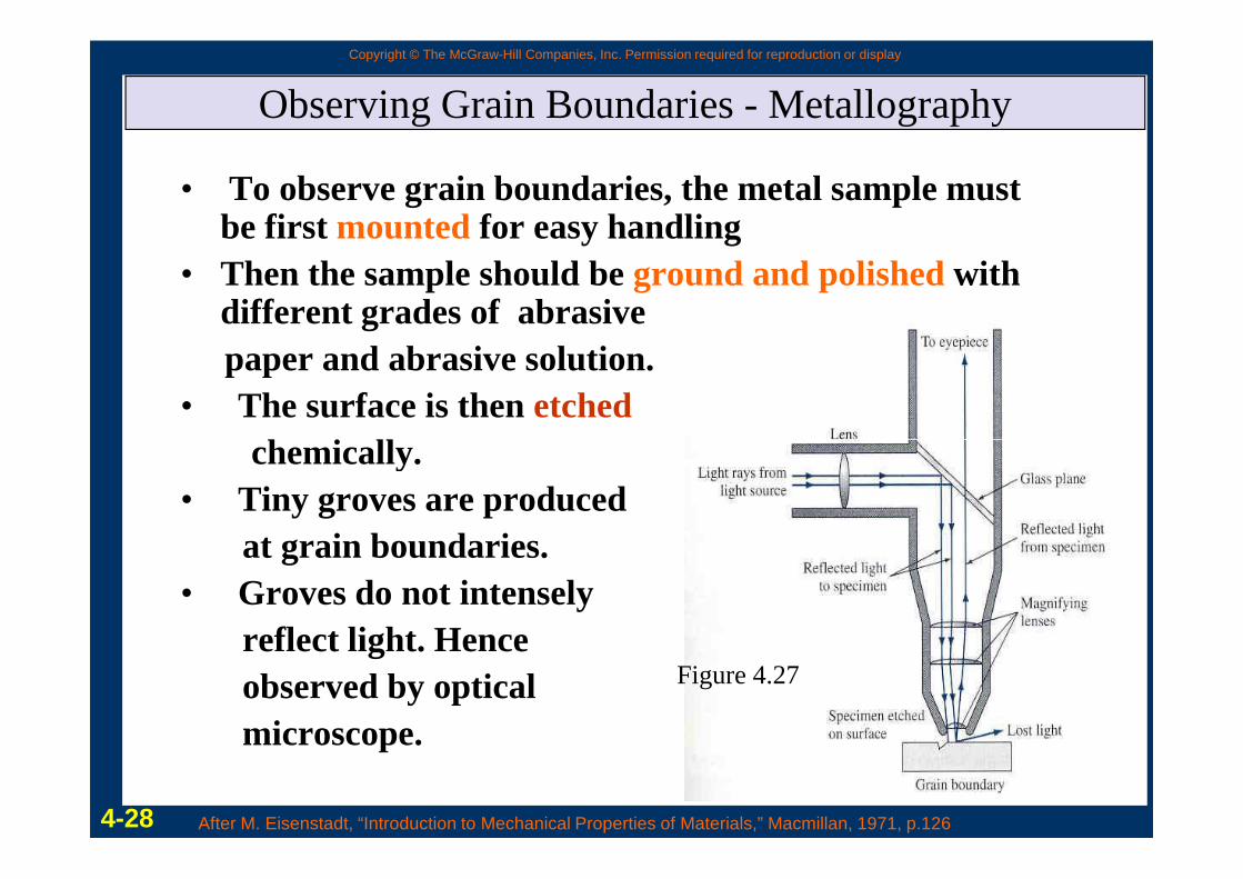
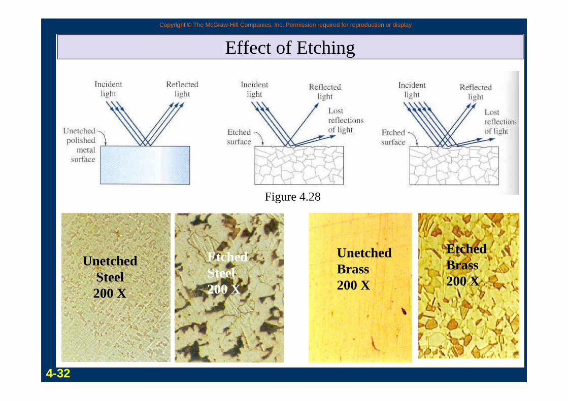
Observing Grain Boundaries - Metallography
• To observe grain boundaries, the metal sample must be first mounted for easy handling
• Then the sample should be ground and polishedwith different grades of abrasive paper and abrasive solution.
• The surface is then etchedchemically. chemically.
• Tiny groves are producedat grain boundaries.
• Groves do not intensely reflect light. Hence observed by opticalmicroscope.
4-28 After M. Eisenstadt, “Introduction to Mechanical Properties of Materials,” Macmillan, 1971, p.126
Figure 4.27
Copyright © The McGraw-Hill Companies, Inc. Permission required for reproduction or display
Grain Size
• Affects the mechanical propertiesof the material
• The smaller the grain size, more are the grain boundaries.
• More grain boundaries means higher resistance to slip (plastic deformation occurs resistance to slip (plastic deformation occurs due to slip).
• More grains means more uniform the mechanical properties are.
4-30
Copyright © The McGraw-Hill Companies, Inc. Permission required for reproduction or display
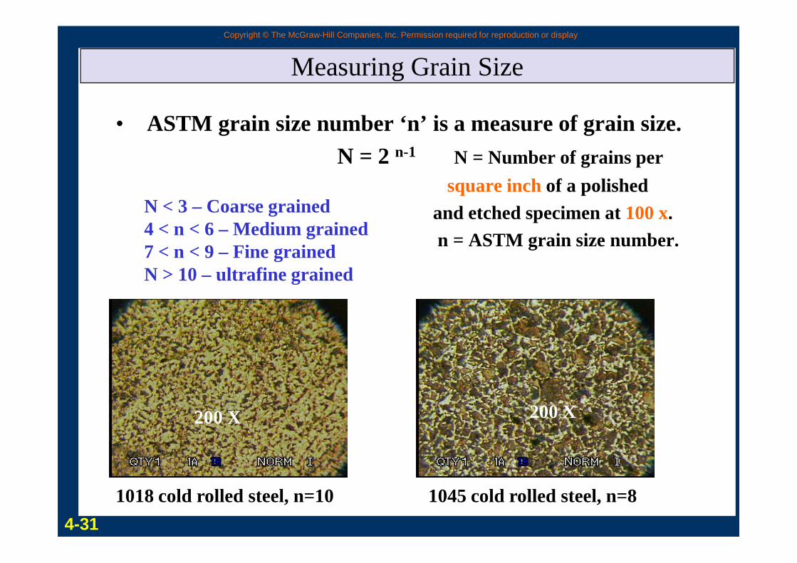
Measuring Grain Size
• ASTM grain size number ‘n’ is a measure of grain size.N = 2 n-1 N = Number of grains per
square inchof a polishedand etched specimen at 100 x.n = ASTM grain size number.
N < 3 – Coarse grained4 < n < 6 – Medium grained7 < n < 9 – Fine grainedN > 10 – ultrafine grained
200 X 200 X
1018 cold rolled steel, n=10 1045 cold rolled steel, n=8
4-31
N > 10 – ultrafine grained
Copyright © The McGraw-Hill Companies, Inc. Permission required for reproduction or display
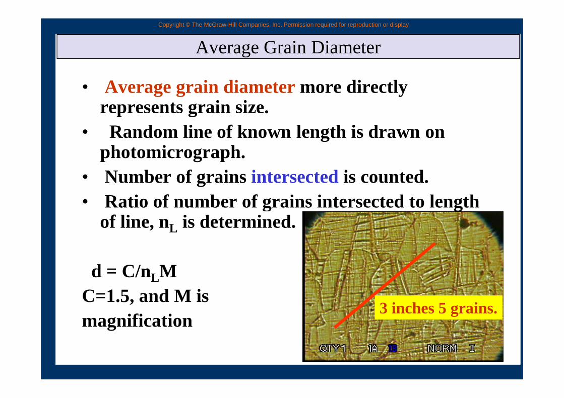
Average Grain Diameter
• Average grain diametermore directly represents grain size.
• Random line of known length is drawn on photomicrograph.
• Number of grains intersectedis counted.• Ratio of number of grains intersected to length • Ratio of number of grains intersected to length
of line, nL is determined.
d = C/nLM C=1.5, and M is magnification
3 inches 5 grains.
Copyright © The McGraw-Hill Companies, Inc. Permission required for reproduction or display
Effect of Etching
Figure 4.28
Unetched Steel200 X
Etched Steel200 X
Unetched Brass200 X
Etched Brass200 X
4-32
Figure 4.28
Copyright © The McGraw-Hill Companies, Inc. Permission required for reproduction or display
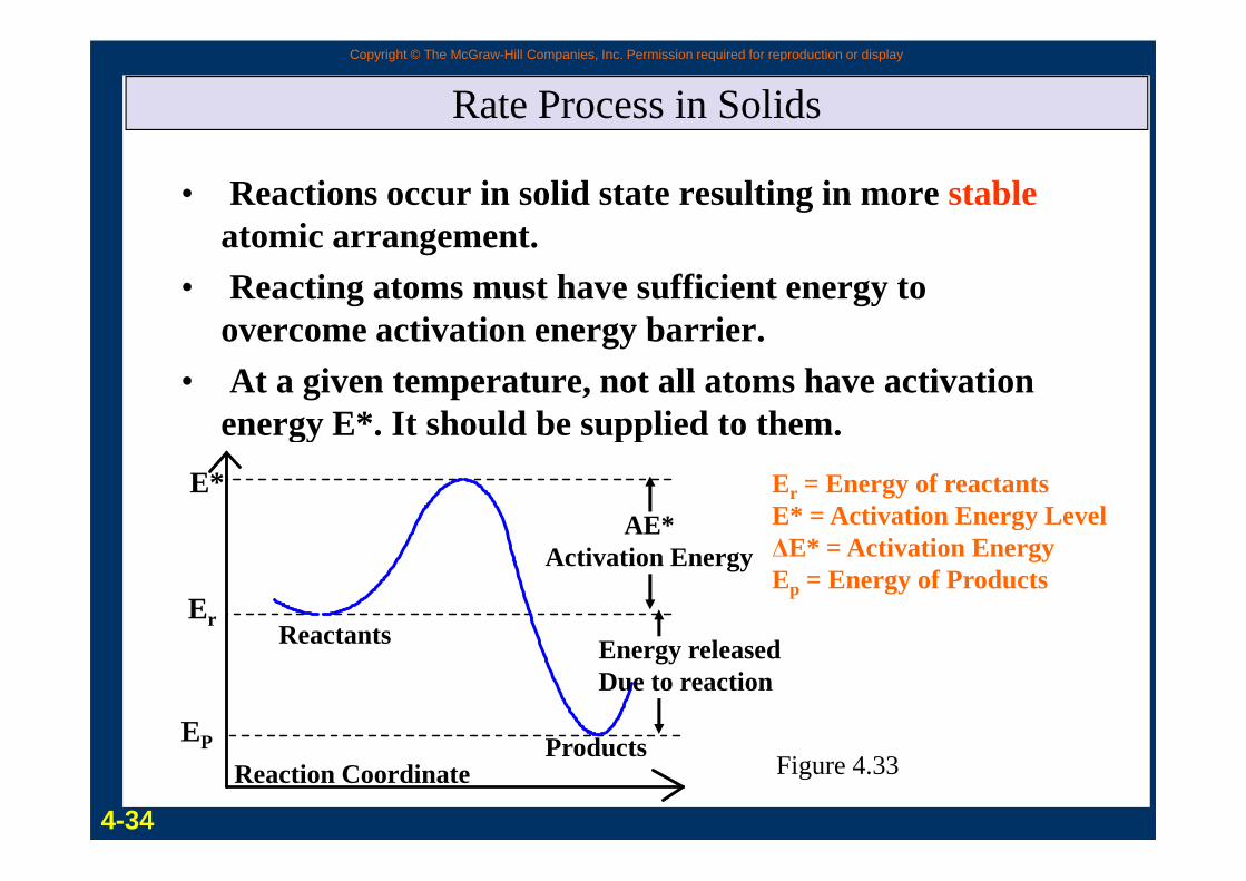
Rate Process in Solids
• Reactions occur in solid state resulting in more stableatomic arrangement.
• Reacting atoms must have sufficient energy to overcome activation energy barrier.
• At a given temperature, not all atoms have activation energy E*. It should be supplied to them. energy E*. It should be supplied to them.
E*
Er
EP
AE*Activation Energy
Energy releasedDue to reaction
Reaction Coordinate
Reactants
Products
Er = Energy of reactantsE* = Activation Energy Level∆E* = Activation EnergyEp = Energy of Products
4-34
Figure 4.33
Copyright © The McGraw-Hill Companies, Inc. Permission required for reproduction or display
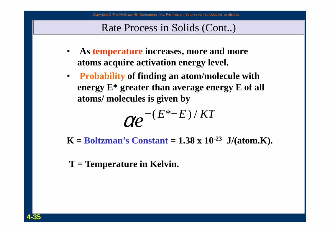
Rate Process in Solids (Cont..)
• As temperature increases, more and more atoms acquire activation energy level.
• Probability of finding an atom/molecule with energy E* greater than average energy E of all atoms/ molecules is given by
KTEEe /)*( −−α KTEEe /)*( −−αK = Boltzman’s Constant= 1.38 x 10⁻²³ J/(atom.K).
T = Temperature in Kelvin.
4-35
Copyright © The McGraw-Hill Companies, Inc. Permission required for reproduction or display
Rate Process in Solids (Cont..)
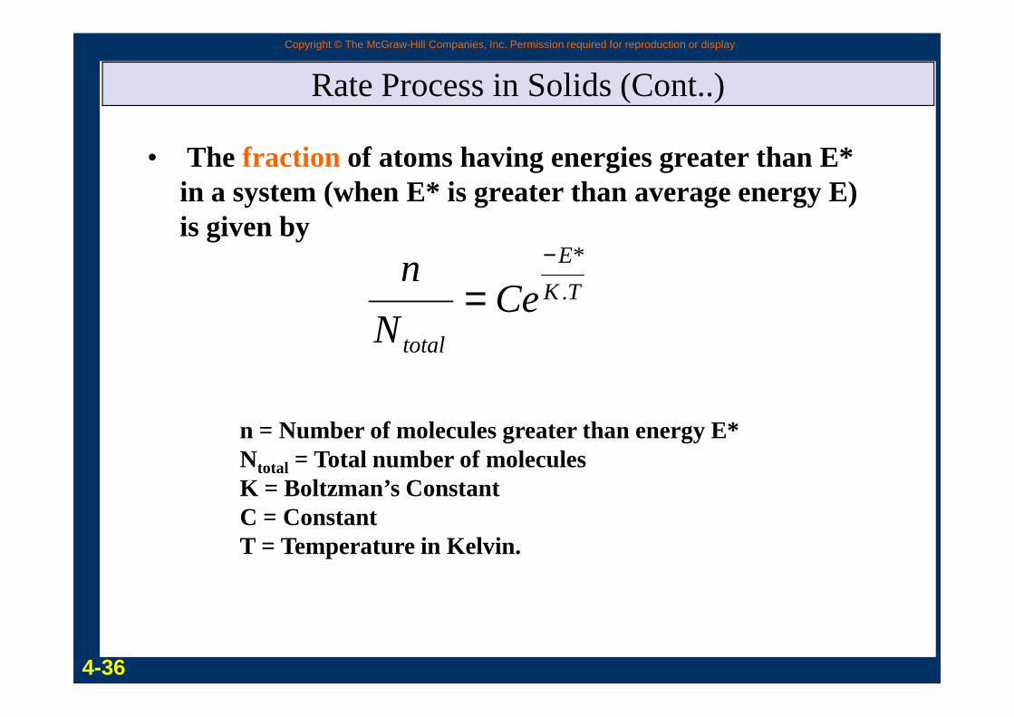
• The fraction of atoms having energies greater than E* in a system (when E* is greater than average energy E) is given by
TK
E
total
CeN
n.
*−
=
n = Number of molecules greater than energy E*Ntotal = Total number of moleculesK = Boltzman’s ConstantC = ConstantT = Temperature in Kelvin.
4-36
Copyright © The McGraw-Hill Companies, Inc. Permission required for reproduction or display
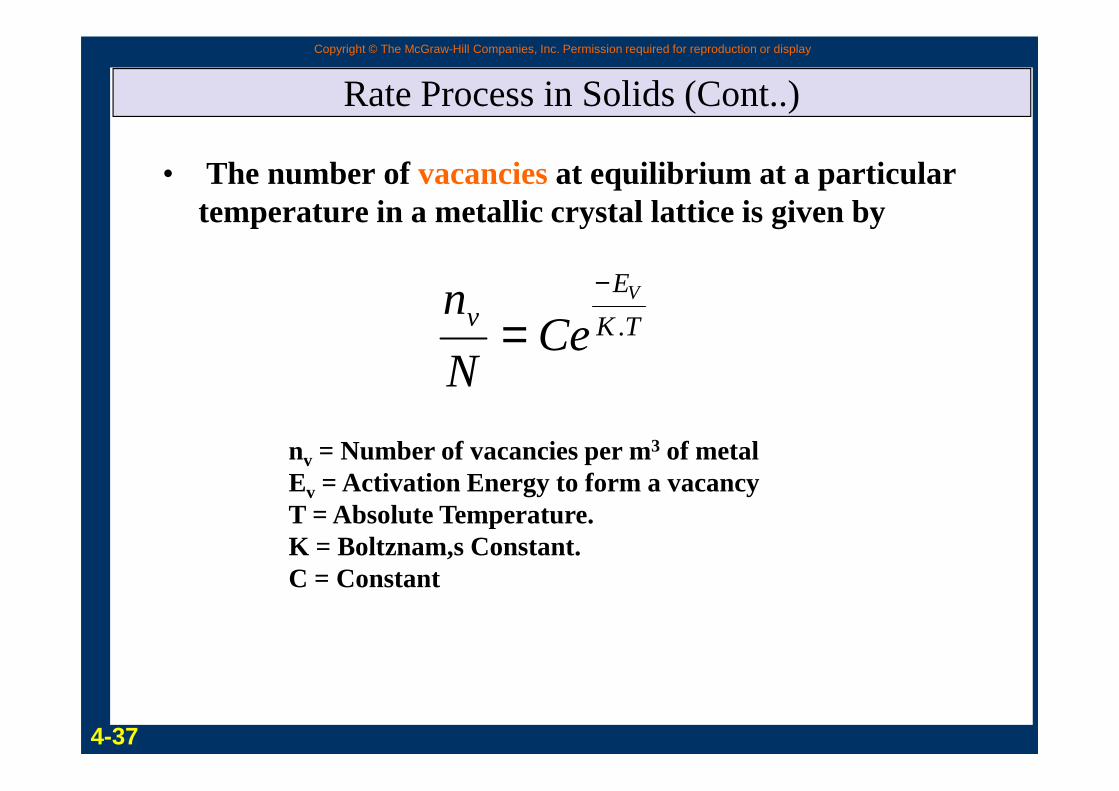
Rate Process in Solids (Cont..)
• The number of vacanciesat equilibrium at a particular temperature in a metallic crystal lattice is given by
TK
Ev
V
CeN
n.
−
=N
nv = Number of vacancies per m3 of metalEv = Activation Energy to form a vacancy T = Absolute Temperature.K = Boltznam,s Constant.C = Constant
4-37
Copyright © The McGraw-Hill Companies, Inc. Permission required for reproduction or display
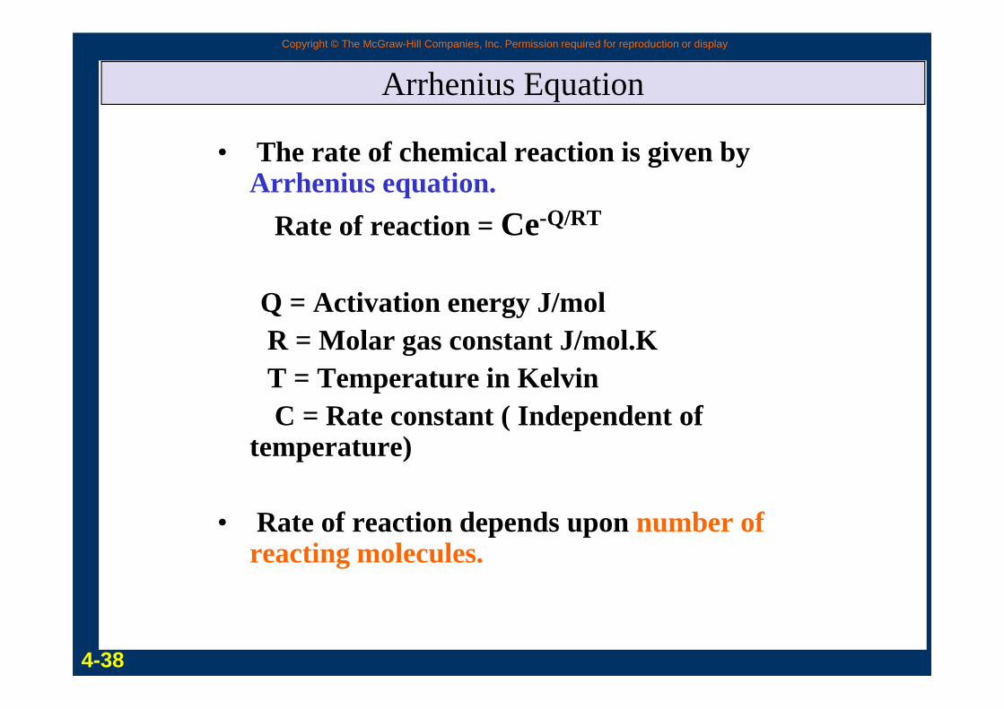
Arrhenius Equation
• The rate of chemical reaction is given by Arrhenius equation.
Rate of reaction = Ce-Q/RT
Q = Activation energy J/molR = Molar gas constant J/mol.KR = Molar gas constant J/mol.KT = Temperature in KelvinC = Rate constant ( Independent of
temperature)
• Rate of reaction depends upon number of reacting molecules.
4-38
Copyright © The McGraw-Hill Companies, Inc. Permission required for reproduction or display
Solidification of Metals
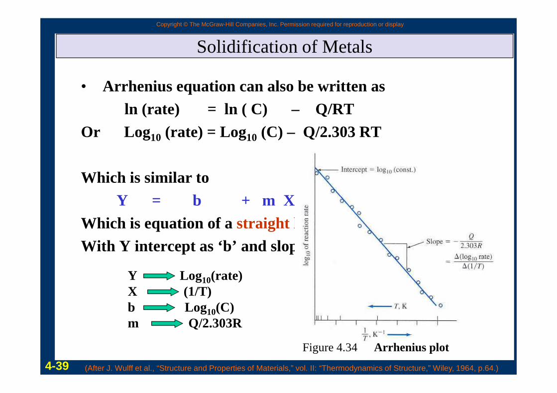
• Arrhenius equation can also be written asln (rate) = ln ( C) – Q/RT
Or Log10 (rate) = Log10 (C) – Q/2.303 RT
Which is similar to Y = b + m XY = b + m X
Which is equation of a straight lineWith Y intercept as ‘b’ and slope ‘m’.
Y Log10(rate)X (1/T)b Log10(C)m Q/2.303R
4-39
Figure 4.34 Arrhenius plot
(After J. Wulff et al., “Structure and Properties of Materials,” vol. II: “Thermodynamics of Structure,” Wiley, 1964, p.64.)