Embed Size (px)
Citation preview

Characterisation and optimisation of PECVD SiNx as an antireflectioncoating and passivation layer for silicon solar cellsYimao Wan, Keith R. McIntosh, and Andrew F. Thomson Citation: AIP Advances 3, 032113 (2013); doi: 10.1063/1.4795108 View online: http://dx.doi.org/10.1063/1.4795108 View Table of Contents: http://aipadvances.aip.org/resource/1/AAIDBI/v3/i3 Published by the American Institute of Physics. Related ArticlesGrowth and band alignment of Bi2Se3 topological insulator on H-terminated Si(111) van der Waals surface Appl. Phys. Lett. 102, 074106 (2013) Effect of microwave plasma treatment on silicon dioxide films grown by atomic layer deposition at lowtemperature J. Appl. Phys. 113, 064102 (2013) Strain engineering in epitaxial La1−xSr1+xMnO4 thin films J. Appl. Phys. 113, 053906 (2013) Synthesis and characterization of MoS2/Ti composite coatings on Ti6Al4V prepared by laser cladding AIP Advances 3, 022106 (2013) Molecular beam epitaxy of high structural quality Bi2Se3 on lattice matched InP(111) substrates Appl. Phys. Lett. 102, 041914 (2013) Additional information on AIP AdvancesJournal Homepage: http://aipadvances.aip.org Journal Information: http://aipadvances.aip.org/about/journal Top downloads: http://aipadvances.aip.org/most_downloaded Information for Authors: http://aipadvances.aip.org/authors
Downloaded 05 Mar 2013 to 150.203.45.141. All article content, except where otherwise noted, is licensed under a Creative Commons Attribution 3.0 Unported license.See: http://creativecommons.org/licenses/by/3.0/
AIP ADVANCES 3, 032113 (2013)
Characterisation and optimisation of PECVD SiNx as anantireflection coating and passivation layer forsilicon solar cells
Yimao Wan,1 Keith R. McIntosh,2 and Andrew F. Thomson1
1Research School of Engineering, The Australian National University (ANU), Canberra ACT0200, Australia2PV Lighthouse, Coledale NSW 2515, Australia
(Received 1 November 2012; accepted 14 February 2013; published online 5 March 2013)
In this work, we investigate how the film properties of silicon nitride (SiNx) de-pend on its deposition conditions when formed by plasma enhanced chemical vapourdeposition (PECVD). The examination is conducted with a Roth & Rau AK400PECVD reactor, where the varied parameters are deposition temperature, pressure,gas flow ratio, total gas flow, microwave plasma power and radio-frequency biasvoltage. The films are evaluated by Fourier transform infrared spectroscopy to de-termine structural properties, by spectrophotometry to determine optical properties,and by capacitance–voltage and photoconductance measurements to determine elec-tronic properties. After reporting on the dependence of SiNx properties on depositionparameters, we determine the optimized deposition conditions that attain low absorp-tion and low recombination. On the basis of SiNx growth models proposed in theliterature and of our experimental results, we discuss how each process parameteraffects the deposition rate and chemical bond density. We then focus on the effectivesurface recombination velocity Seff, which is of primary importance to solar cells.We find that for the SiNx prepared in this work, 1) Seff does not correlate universallywith the bulk structural and optical properties such as chemical bond densities andrefractive index, and 2) Seff depends primarily on the defect density at the SiNx-Siinterface rather than the insulator charge. Finally, employing the optimized depo-sition condition, we achieve a relatively constant and low Seff,UL on low-resistivity(≤1.1 �cm) p- and n-type c-Si substrates over a broad range of n = 1.85–4.07.The results of this study demonstrate that the trade-off between optical transmissionand surface passivation can be circumvented. Although we focus on photovoltaicapplications, this study may be useful for any device for which it is desirable tomaximize light transmission and surface passivation. Copyright 2013 Author(s). Thisarticle is distributed under a Creative Commons Attribution 3.0 Unported License.[http://dx.doi.org/10.1063/1.4795108]
I. INTRODUCTION
An antireflection coating (ARC) is an important feature of crystalline silicon solar cells. Ide-ally, this layer should not only maximize optical transmission but simultaneously suppress surfacerecombination. Amorphous hydrogenated silicon nitride a-SiNx:H (hereafter referred to as SiNx)synthesised by low-temperature PECVD has become the state-of-the-art ARC layer for c-Si solarcells to fulfil these two requirements.1, 2 It also provides a humidity barrier, protecting underlyinginterfaces from the degrading effects of moisture,3, 4 and is a source of hydrogen for passivatingsilicon bulk defects.5–8
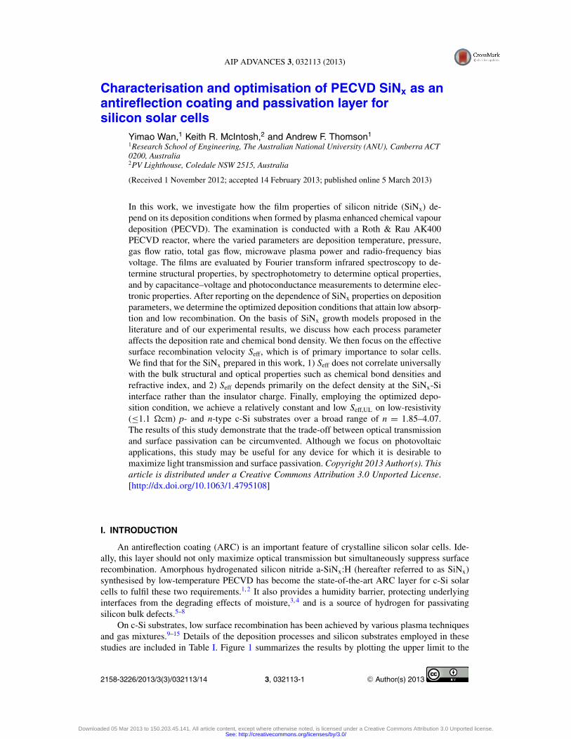
On c-Si substrates, low surface recombination has been achieved by various plasma techniquesand gas mixtures.9–15 Details of the deposition processes and silicon substrates employed in thesestudies are included in Table I. Figure 1 summarizes the results by plotting the upper limit to the
2158-3226/2013/3(3)/032113/14 C© Author(s) 20133, 032113-1
Downloaded 05 Mar 2013 to 150.203.45.141. All article content, except where otherwise noted, is licensed under a Creative Commons Attribution 3.0 Unported license.See: http://creativecommons.org/licenses/by/3.0/
032113-2 Wan, McIntosh, and Thomson AIP Advances 3, 032113 (2013)
TABLE I. Summary on the details of PECVD processes and silicon substrates employed in references.
Substrateb Lowest Seff,UL andPECVD process detailsa (FZ, {100} p-Si) associated n
Technique T (oC) Reactant gas mixture ρbulk (� · cm) W (μm) Seff,ULe (cm/s) n at 632 nm Refs.
Remote lab 375c SiH4, NH3 1.50 300 11.5 2.4 9Direct HF lab 350d SiH4, NH3, diluted H2 1.25 250 7.5 3.2 10Remote inline 350d SiH4, NH3, diluted H2 1.50 300 10.3 2.7 11Direct LF lab 370d SiH4, NH3 5.00 300 13.5 3.0 12Remote inline 450d SiH4, NH3 1.50 280 5.9 2.5 13Direct HF lab 400d SiH4, NH3, diluted N2 1.00 400 17.9 1.9 14Dual-mode lab 290c SiH4, NH3,Ar 0.85 300 1.6 1.9 15
aProcess variable altered in Refs. 10–13 is gas flow ratio.bFZ-float zone; ρbulk-nominal bulk resistivity; W-silicon substrate width.cMeasured temperature on substrate table by thermal coupler.dTemperature setpoint.eSeff,UL is cited at excess carrier density �n = 1015 cm−3 and recalculated using the latest Auger model.16
FIG. 1. The upper limit to the effective surface recombination velocity Seff,UL as a function of refractive index n at 632 nm forSiNx-passivated FZ p-Si substrates. SiNx is deposited by a variety of deposition techniques and gas mixtures as summarisedin Table I. The dash-line highlights the opposing trend presented in Ref. 15.
effective surface recombination velocity Seff,UL as a function of the refractive index n. The presentedSeff,UL and n are at an excess carrier density of �n = 1015 cm−3 and a wavelength of 632 nm,respectively. As can be seen, irrespective of deposition techniques and reactant gas mixtures em-ployed in Refs. 10, 12, and 13 an apparent trend is observed: Seff,UL decreases as n increases. Morecomplicated trends can be observed for the results in Refs. 9 and 11, whereby Seff,UL first decreaseswith increasing n and saturates for n above 2.3.
The results presented in Refs. 9–13 make it appear that the optimum surface passivation isacquired by Si-rich SiNx of high n. Since high-n SiNx is well-known to be highly absorbing of shortwavelength light, this trend implies there is a trade-off between optical transmission and surfacepassivation. However, two previous studies suggest that the trade-off can be circumvented: Schmidtet al.14 achieved a low Seff,UL (15.2 cm/s on FZ 1.0-� · cm p-Si) using a stoichiometric SiNx (n = 1.9)by including N2 with SiH4 and NH3, and our recent work15 presented a low Seff,UL (1.6 cm/s on FZ0.85-� · cm p-Si, and lower still on FZ 0.47-� · cm n-Si) by low absorption SiNx. The key process
Downloaded 05 Mar 2013 to 150.203.45.141. All article content, except where otherwise noted, is licensed under a Creative Commons Attribution 3.0 Unported license.See: http://creativecommons.org/licenses/by/3.0/
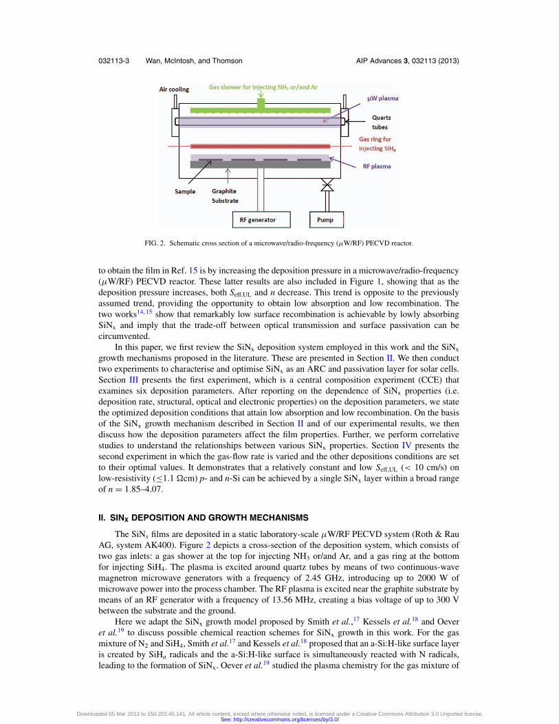
032113-3 Wan, McIntosh, and Thomson AIP Advances 3, 032113 (2013)
FIG. 2. Schematic cross section of a microwave/radio-frequency (μW/RF) PECVD reactor.
to obtain the film in Ref. 15 is by increasing the deposition pressure in a microwave/radio-frequency(μW/RF) PECVD reactor. These latter results are also included in Figure 1, showing that as thedeposition pressure increases, both Seff,UL and n decrease. This trend is opposite to the previouslyassumed trend, providing the opportunity to obtain low absorption and low recombination. Thetwo works14, 15 show that remarkably low surface recombination is achievable by lowly absorbingSiNx and imply that the trade-off between optical transmission and surface passivation can becircumvented.
In this paper, we first review the SiNx deposition system employed in this work and the SiNx
growth mechanisms proposed in the literature. These are presented in Section II. We then conducttwo experiments to characterise and optimise SiNx as an ARC and passivation layer for solar cells.Section III presents the first experiment, which is a central composition experiment (CCE) thatexamines six deposition parameters. After reporting on the dependence of SiNx properties (i.e.deposition rate, structural, optical and electronic properties) on the deposition parameters, we statethe optimized deposition conditions that attain low absorption and low recombination. On the basisof the SiNx growth mechanism described in Section II and of our experimental results, we thendiscuss how the deposition parameters affect the film properties. Further, we perform correlativestudies to understand the relationships between various SiNx properties. Section IV presents thesecond experiment in which the gas-flow rate is varied and the other depositions conditions are setto their optimal values. It demonstrates that a relatively constant and low Seff,UL (< 10 cm/s) onlow-resistivity (≤1.1 �cm) p- and n-Si can be achieved by a single SiNx layer within a broad rangeof n = 1.85–4.07.
II. SINX DEPOSITION AND GROWTH MECHANISMS
The SiNx films are deposited in a static laboratory-scale μW/RF PECVD system (Roth & RauAG, system AK400). Figure 2 depicts a cross-section of the deposition system, which consists oftwo gas inlets: a gas shower at the top for injecting NH3 or/and Ar, and a gas ring at the bottomfor injecting SiH4. The plasma is excited around quartz tubes by means of two continuous-wavemagnetron microwave generators with a frequency of 2.45 GHz, introducing up to 2000 W ofmicrowave power into the process chamber. The RF plasma is excited near the graphite substrate bymeans of an RF generator with a frequency of 13.56 MHz, creating a bias voltage of up to 300 Vbetween the substrate and the ground.
Here we adapt the SiNx growth model proposed by Smith et al.,17 Kessels et al.18 and Oeveret al.19 to discuss possible chemical reaction schemes for SiNx growth in this work. For the gasmixture of N2 and SiH4, Smith et al.17 and Kessels et al.18 proposed that an a-Si:H-like surface layeris created by SiHa radicals and the a-Si:H-like surface is simultaneously reacted with N radicals,leading to the formation of SiNx. Oever et al.19 studied the plasma chemistry for the gas mixture of
Downloaded 05 Mar 2013 to 150.203.45.141. All article content, except where otherwise noted, is licensed under a Creative Commons Attribution 3.0 Unported license.See: http://creativecommons.org/licenses/by/3.0/
032113-4 Wan, McIntosh, and Thomson AIP Advances 3, 032113 (2013)
NH3, SiH4 and Ar and refined the growth model, concluding that SiNx is formed by the direct surfacereaction between the a-Si:H-like layer and NHb radicals. We adapt the abovementioned models andrefine a simple reaction scheme for SiNx growth in this work:
(i) Gas phase dissociation:–NH3 is introduced into the system through the shower-head which forms part of the ceilingof the deposition chamber above the μW quartz tubes and is dissociated:
NH3 + e → NHb + H3−b + e (a)
–SiH4 is fed from the downstream gas ring that is between the quartz tube and RF-biasedgraphite substrate and is dissociated:
SiH4 + e → SiHa + H4−a + e (b)
(ii) Formation/insertion:An a-Si:H-like layer is formed on the silicon wafer by SiHa radicals and simultaneouslyinserted with NHb radicals.
(iii) Film densification by cross-linking at elevated substrate temperature to break Si–H and N–Hand form Si–N:
Si–H + N–H → Si–N + H2 (c)
Concurrently, the excessive incorporation of NHb radicals breaks and replaces the existingSi–H bonds (at elevated substrate temperature), forming Si–N:
Si–H + NHb → Si–N + Hb+1 (d)
or otherwise, the excessive incorporation of SiHa radicals breaks and replaces the existingN–H bonds, forming Si–N:
N–H + SiHa → Si–N + Ha+1. (e)
III. EXPERIMENT 1: CENTRAL COMPOSITION EXPERIMENT
For the optimization of six deposition parameters, we performed the CCE that consisted of 28different deposition conditions (parameter sets) and four additional replications of the baseline. Eachset of experiments involved varying one deposition parameter while keeping the other parametersconstant and at their baseline value. The relationships between SiNx properties and individualdeposition parameters are described and discussed in this section.
A. Experimental details
Table II presents the baseline and range of the deposition parameters varied in this work. It iscommon to have an offset between the set-point of the substrate table temperature and the actualsilicon sample temperature,9, 11 so all deposition temperatures reported here refer to the actual wafertemperature measured by an external calibrated thermocouple, and not to the reactor’s set-pointtemperature.
The lifetime samples in this experiment were p-type {100} FZ-Si wafers with a resistivity of0.85 � · cm and a thickness of 300 μm. All samples were etched in tetramethylammonium hydroxide(TMAH) at ∼85 ◦C to remove saw damage. The p-Si samples were cleaned by the RCA procedureand diffused with phosphorus to getter iron and other metallic impurities.20 The phosphorus glasswas then removed in HF acid and the phosphorus-doped silicon layer was removed by etching ina 1:10 HF:HNO3 solution. Next, all wafers were cleaned by the RCA procedure, dipped in HF toremove the native oxide, and then coated with SiNx on both surfaces by two sequential depositions.
Downloaded 05 Mar 2013 to 150.203.45.141. All article content, except where otherwise noted, is licensed under a Creative Commons Attribution 3.0 Unported license.See: http://creativecommons.org/licenses/by/3.0/
032113-5 Wan, McIntosh, and Thomson AIP Advances 3, 032113 (2013)
TABLE II. Baseline and tested range of PECVD deposition parameters.
Baseline Range
Temperature (◦C) 235 165–405Pressure (mbar) 0.2 0.02–0.50NH3/SiH4 gas flow ratioa 1.0 0.3–3.0Total gas flow (sccm)b 60 30–240μW plasma power (W) 500 50–1000RF Bias voltage (V) 150 75–250
aAr gas flow is kept constant at 20 sccm.bsccm denotes cubic centimetre per minute at standard temperature and pressure.
The effective carrier lifetime τ eff of the samples was measured using a Sinton Instruments WCT-120 operated in either transient or generalized quasi-steady-state mode, as described elsewhere.21
The Seff,UL(�n) can be calculated according to
Seff,UL = w
2
(1
τeff− 1
τbulk,intrinsic
), (1)
Where W is the Si substrate thickness and τ bulk,intrinsic is the Si intrinsic bulk lifetime parameterizedby Richter et al.16
Reflectance and C-V measurements were performed on double-side-polished n-type {100}FZ-Si with a resistivity of 1.0 � · cm and a thickness of 290 μm. Metal-insulator-semiconductor(MIS) test structures were fabricated for C-V measurements. In this work, the front metal contact wasformed by evaporating aluminum through a shadow mask to create circular dots of diameter ∼700 μmand thickness ∼100 nm. The rear contact was formed with a GaIn eutectic. More details on thefabrication of reflectance and C-V measurements samples, as well as the characterisation of thewavelength-dependent refractive index n(λ) and extinction coefficient k(λ), and the interface defectdensity Dit and effective insulator charge Qeff associated with SiNx, can be found in Ref. 15.
The FTIR transmission spectra were measured on the same samples as used for reflectance andC-V measurements, using FTIR spectrometer (Bruker Vertex 80V) with a resolution of 6 cm−1.The measurement showed three distinctive absorption peaks associated with Si–N, Si–H and N–Hvibrational modes about 850, 2220 and 3340 cm−1, respectively.22 The bond density [A–B], definedas the number of bonds per unit volume, can be determined by23
[A–B] = kA–B
∫α(ω)
ωdω, (2)
where α(ω) is the absorption coefficient at wavenumber ω, kA–B is the proportionality constantin cm−2. In this work, kA–B for Si–N, Si–H and N–H is taken from Ref. 22 having the values of2 × 1019, 2 × 10²⁰ and 1.2 × 10²⁰, respectively.
B. Results and discussion
1. Dependence of film properties on deposition parameters
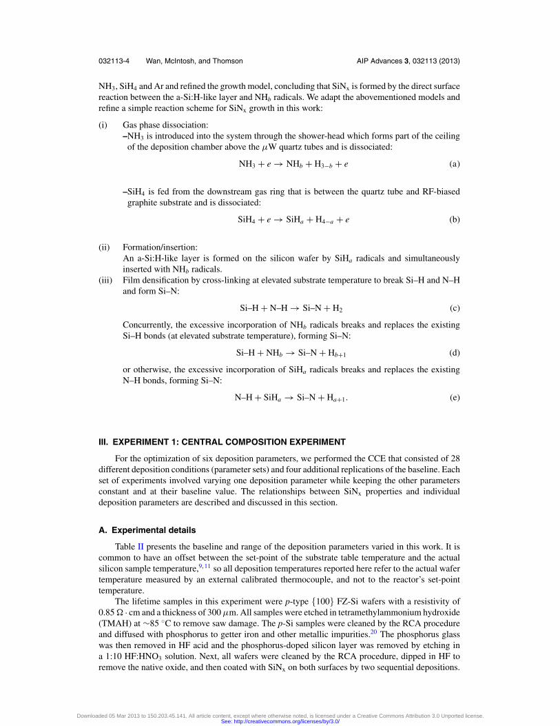
Figure 3 plots the dependence of the deposition rate, bond densities, optical and electronicproperties of plasma SiNx on the various deposition parameters. These dependencies are nowdescribed.
Deposition rate—For throughput considerations, the deposition rate by PECVD should be ashigh as possible. Figure 3(a) shows the effect of deposition parameters on the deposition rate. Thedeposition time for all conditions was 3 min, and the resulting film thickness ranged from 50 to200 nm. We found that increasing the total gas flow within the tested range causes a threefoldincrease in the deposition rate. The factor increase is ∼2 for the decrease of NH3/SiH4 gas flow ratioand smaller (∼1.2) for the variation of other parameters.
Downloaded 05 Mar 2013 to 150.203.45.141. All article content, except where otherwise noted, is licensed under a Creative Commons Attribution 3.0 Unported license.See: http://creativecommons.org/licenses/by/3.0/
032113-6 Wan, McIntosh, and Thomson AIP Advances 3, 032113 (2013)
FIG. 3. Main effects plots of SiNx (a) deposition rate; (b) chemical bond densities; (c) refractive index n at 632 nm andextinction coefficient k at 360 nm; (d) extracted surface recombination velocity Seff,UL at �n = 1015 cm−3 on FZ, 0.85 � cm,{100} 300 μm p-type c-Si.
Bond densities—Figure 3(b) shows the influence of deposition parameters on the SiNx chemicalbond densities, namely [Si–N], [N–H] and [Si–H]. [Si–N] exhibits a peak within the tested rangeof all the parameters, except for temperature, for which [Si–N] increases as temperature increases.When deposition pressure, gas flow ratio and plasma power are increased, and when total gas flow isdecreased, the hydrogen-bond concentrations, [N–H] and [Si–H] tend to exhibit inverse relationships,where [N–H] increases moderately and [Si–H] decreases strongly. This trend is consistent with thefilms becoming less Si-rich. Exceptions to this inverse correlation is that both [N–H] and [Si–H]decrease moderately as temperature increases and RF bias decreases.
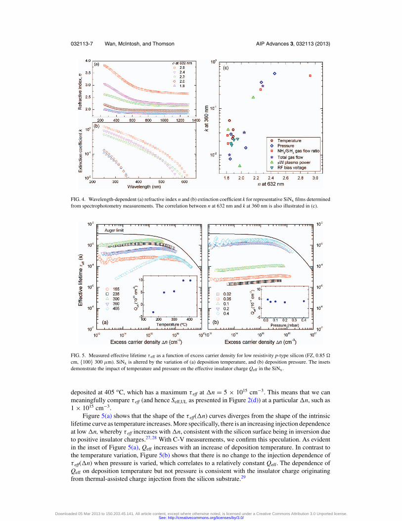
Optical properties—Figure 3(c) depicts the responses of n at 632 nm and k at 360 nm to thedeposition parameters. As we can see, n decreases strongly with increasing NH3/SiH4 gas flow ratio,μW plasma power, pressure and total gas flow, whereas it is hardly affected by the variation ofdeposition temperature and RF bias voltage. Moreover, Figure 4(a) and 4(b) show the dispersionrelation for both the refractive index n and the extinction coefficient k. The results are consistentwith those reported in other studies,24–26 showing a decrease of n and k with increasing wavelength.As expected, SiNx of low n (≤2.0) exhibits low absorption of short-wavelength light and almostnegligible absorption at wavelengths above 360 nm, implying it is better suited as the ARC insolar cells. Indeed, compared to the SiNx of n = 2.5 and an equivalent passivation, the opticalsimulation of our previous work15 found that the SiNx of n = 1.9 would enhance the photogeneratedcurrent density by more 0.66 mA/cm−2 or 1.40 mA/cm−2 for solar cells encapsulated in glass andethylene-vinyl acetate (EVA) or operating in air, respectively. This enhancement is due to the film’slow k rather than it having the optimum n. In addition, we find that, irrespective of the variation ofdeposition parameters, an increase of k at 360 nm is generally accompanied by an increase of n at632 nm, as made clearer with Figure 4(c).
Surface passivation—Figure 3(d) plots Seff,UL of the as-deposited SiNx. It indicates that Seff,UL
depends strongly on deposition temperature, pressure and gas flow ratio, and slightly on total gasflow, μW plasma power and RF bias voltage. Whereas Seff,UL increases with increasing NH3/SiH4 gasflow ratio, Seff,UL decreases significantly as pressure increases. An optimum deposition temperatureis observed at 300 ◦C, leading to a minimum Seff,UL.
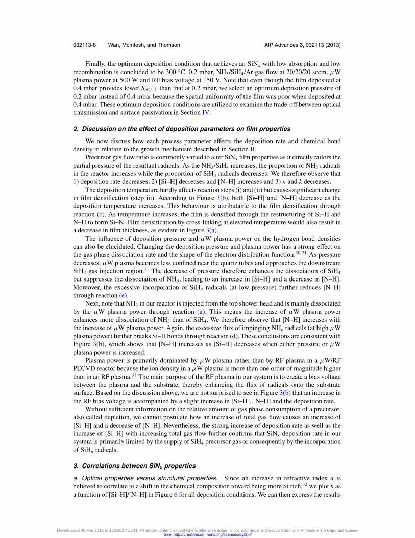
Figure 5 shows the injection-dependent effective lifetime τ eff(�n) for SiNx-passivated p-typesilicon samples. We briefly comment on how τ eff(�n) is affected by temperature and pressure sincepassivation is the most sensitive to these parameters. For reference, the Auger limit parameterizedby Richter et al. is also plotted.16 We note that none of the τ eff(�n) curves cross over except for SiNx
Downloaded 05 Mar 2013 to 150.203.45.141. All article content, except where otherwise noted, is licensed under a Creative Commons Attribution 3.0 Unported license.See: http://creativecommons.org/licenses/by/3.0/
032113-7 Wan, McIntosh, and Thomson AIP Advances 3, 032113 (2013)
FIG. 4. Wavelength-dependent (a) refractive index n and (b) extinction coefficient k for representative SiNx films determinedfrom spectrophotometry measurements. The correlation between n at 632 nm and k at 360 nm is also illustrated in (c).
FIG. 5. Measured effective lifetime τ eff as a function of excess carrier density for low resistivity p-type silicon (FZ, 0.85 �
cm, {100} 300 μm). SiNx is altered by the variation of (a) deposition temperature, and (b) deposition pressure. The insetsdemonstrate the impact of temperature and pressure on the effective insulator charge Qeff in the SiNx.
deposited at 405 oC, which has a maximum τ eff at �n = 5 × 1015 cm−3. This means that we canmeaningfully compare τ eff (and hence Seff,UL as presented in Figure 2(d)) at a particular �n, such as1 × 1015 cm−3.
Figure 5(a) shows that the shape of the τ eff(�n) curves diverges from the shape of the intrinsiclifetime curve as temperature increases. More specifically, there is an increasing injection dependenceat low �n, whereby τ eff increases with �n, consistent with the silicon surface being in inversion dueto positive insulator charges.27, 28 With C-V measurements, we confirm this speculation. As evidentin the inset of Figure 5(a), Qeff increases with an increase of deposition temperature. In contrast tothe temperature variation, Figure 5(b) shows that there is no change to the injection dependence ofτ eff(�n) when pressure is varied, which correlates to a relatively constant Qeff. The dependence ofQeff on deposition temperature but not pressure is consistent with the insulator charge originatingfrom thermal-assisted charge injection from the silicon substrate.29
Downloaded 05 Mar 2013 to 150.203.45.141. All article content, except where otherwise noted, is licensed under a Creative Commons Attribution 3.0 Unported license.See: http://creativecommons.org/licenses/by/3.0/
032113-8 Wan, McIntosh, and Thomson AIP Advances 3, 032113 (2013)
Finally, the optimum deposition condition that achieves an SiNx with low absorption and lowrecombination is concluded to be 300 ◦C, 0.2 mbar, NH3/SiH4/Ar gas flow at 20/20/20 sccm, μWplasma power at 500 W and RF bias voltage at 150 V. Note that even though the film deposited at0.4 mbar provides lower Seff,UL than that at 0.2 mbar, we select an optimum deposition pressure of0.2 mbar instead of 0.4 mbar because the spatial uniformity of the film was poor when deposited at0.4 mbar. These optimum deposition conditions are utilized to examine the trade-off between opticaltransmission and surface passivation in Section IV.
2. Discussion on the effect of deposition parameters on film properties
We now discuss how each process parameter affects the deposition rate and chemical bonddensity in relation to the growth mechanism described in Section II.
Precursor gas flow ratio is commonly varied to alter SiNx film properties as it directly tailors thepartial pressure of the resultant radicals. As the NH3/SiH4 increases, the proportion of NHb radicalsin the reactor increases while the proportion of SiHa radicals decreases. We therefore observe that1) deposition rate decreases, 2) [Si–H] decreases and [N–H] increases and 3) n and k decreases.
The deposition temperature hardly affects reaction steps (i) and (ii) but causes significant changein film densification (step iii). According to Figure 3(b), both [Si–H] and [N–H] decrease as thedeposition temperature increases. This behaviour is attributable to the film densification throughreaction (c). As temperature increases, the film is densified through the restructuring of Si–H andN–H to form Si–N. Film densification by cross-linking at elevated temperature would also result ina decrease in film thickness, as evident in Figure 3(a).
The influence of deposition pressure and μW plasma power on the hydrogen bond densitiescan also be elucidated. Changing the deposition pressure and plasma power has a strong effect onthe gas phase dissociation rate and the shape of the electron distribution function.30, 31 As pressuredecreases, μW plasma becomes less confined near the quartz tubes and approaches the downstreamSiH4 gas injection region.11 The decrease of pressure therefore enhances the dissociation of SiH4
but suppresses the dissociation of NH3, leading to an increase in [Si–H] and a decrease in [N–H].Moreover, the excessive incorporation of SiHa radicals (at low pressure) further reduces [N–H]through reaction (e).
Next, note that NH3 in our reactor is injected from the top shower head and is mainly dissociatedby the μW plasma power through reaction (a). This means the increase of μW plasma powerenhances more dissociation of NH3 than of SiH4. We therefore observe that [N–H] increases withthe increase of μW plasma power. Again, the excessive flux of impinging NHb radicals (at high μWplasma power) further breaks Si–H bonds through reaction (d). These conclusions are consistent withFigure 3(b), which shows that [N–H] increases as [Si–H] decreases when either pressure or μWplasma power is increased.
Plasma power is primarily dominated by μW plasma rather than by RF plasma in a μW/RFPECVD reactor because the ion density in a μW plasma is more than one order of magnitude higherthan in an RF plasma.31 The main purpose of the RF plasma in our system is to create a bias voltagebetween the plasma and the substrate, thereby enhancing the flux of radicals onto the substratesurface. Based on the discussion above, we are not surprised to see in Figure 3(b) that an increase inthe RF bias voltage is accompanied by a slight increase in [Si–H], [N–H] and the deposition rate.
Without sufficient information on the relative amount of gas phase consumption of a precursor,also called depletion, we cannot postulate how an increase of total gas flow causes an increase of[Si–H] and a decrease of [N–H]. Nevertheless, the strong increase of deposition rate as well as theincrease of [Si–H] with increasing total gas flow further confirms that SiNx deposition rate in oursystem is primarily limited by the supply of SiH4 precursor gas or consequently by the incorporationof SiHa radicals.
3. Correlations between SiNx properties
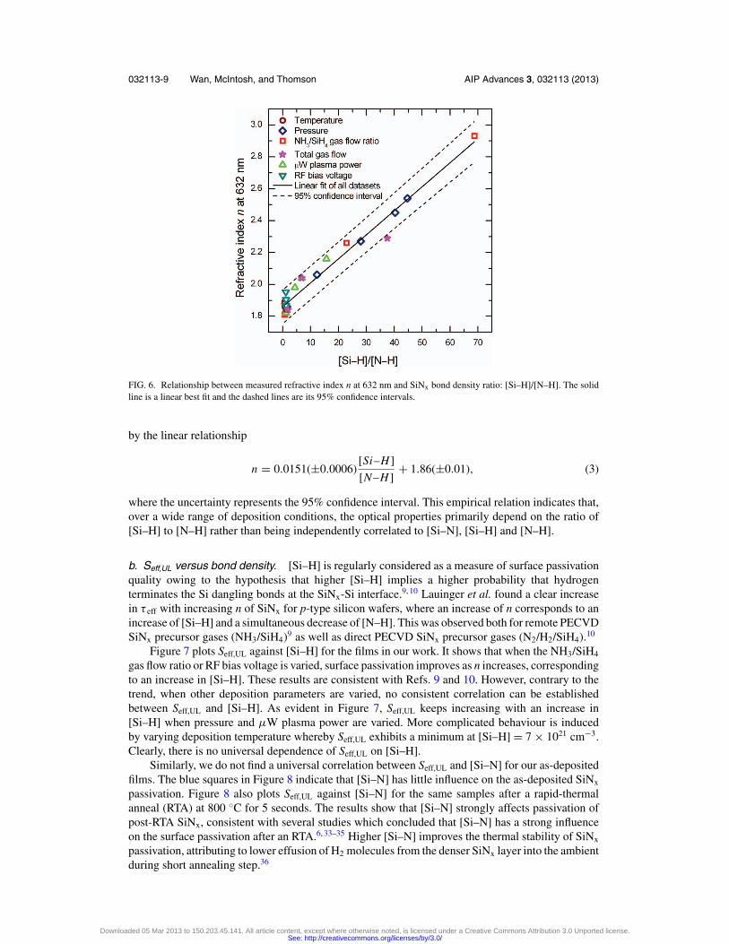
a. Optical properties versus structural properties. Since an increase in refractive index n isbelieved to correlate to a shift in the chemical composition toward being more Si rich,32 we plot n asa function of [Si–H]/[N–H] in Figure 6 for all deposition conditions. We can then express the results
Downloaded 05 Mar 2013 to 150.203.45.141. All article content, except where otherwise noted, is licensed under a Creative Commons Attribution 3.0 Unported license.See: http://creativecommons.org/licenses/by/3.0/
032113-9 Wan, McIntosh, and Thomson AIP Advances 3, 032113 (2013)
FIG. 6. Relationship between measured refractive index n at 632 nm and SiNx bond density ratio: [Si–H]/[N–H]. The solidline is a linear best fit and the dashed lines are its 95% confidence intervals.
by the linear relationship
n = 0.0151(±0.0006)[Si–H ]
[N–H ]+ 1.86(±0.01), (3)
where the uncertainty represents the 95% confidence interval. This empirical relation indicates that,over a wide range of deposition conditions, the optical properties primarily depend on the ratio of[Si–H] to [N–H] rather than being independently correlated to [Si–N], [Si–H] and [N–H].
b. Seff,UL versus bond density. [Si–H] is regularly considered as a measure of surface passivationquality owing to the hypothesis that higher [Si–H] implies a higher probability that hydrogenterminates the Si dangling bonds at the SiNx-Si interface.9, 10 Lauinger et al. found a clear increasein τ eff with increasing n of SiNx for p-type silicon wafers, where an increase of n corresponds to anincrease of [Si–H] and a simultaneous decrease of [N–H]. This was observed both for remote PECVDSiNx precursor gases (NH3/SiH4)9 as well as direct PECVD SiNx precursor gases (N2/H2/SiH4).10
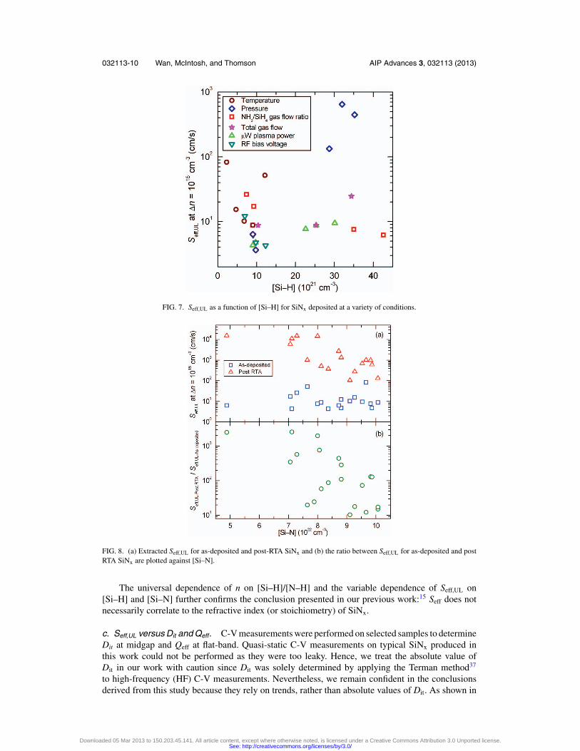
Figure 7 plots Seff,UL against [Si–H] for the films in our work. It shows that when the NH3/SiH4
gas flow ratio or RF bias voltage is varied, surface passivation improves as n increases, correspondingto an increase in [Si–H]. These results are consistent with Refs. 9 and 10. However, contrary to thetrend, when other deposition parameters are varied, no consistent correlation can be establishedbetween Seff,UL and [Si–H]. As evident in Figure 7, Seff,UL keeps increasing with an increase in[Si–H] when pressure and μW plasma power are varied. More complicated behaviour is inducedby varying deposition temperature whereby Seff,UL exhibits a minimum at [Si–H] = 7 × 1021 cm−3.Clearly, there is no universal dependence of Seff,UL on [Si–H].
Similarly, we do not find a universal correlation between Seff,UL and [Si–N] for our as-depositedfilms. The blue squares in Figure 8 indicate that [Si–N] has little influence on the as-deposited SiNx
passivation. Figure 8 also plots Seff,UL against [Si–N] for the same samples after a rapid-thermalanneal (RTA) at 800 ◦C for 5 seconds. The results show that [Si–N] strongly affects passivation ofpost-RTA SiNx, consistent with several studies which concluded that [Si–N] has a strong influenceon the surface passivation after an RTA.6, 33–35 Higher [Si–N] improves the thermal stability of SiNx
passivation, attributing to lower effusion of H2 molecules from the denser SiNx layer into the ambientduring short annealing step.36
Downloaded 05 Mar 2013 to 150.203.45.141. All article content, except where otherwise noted, is licensed under a Creative Commons Attribution 3.0 Unported license.See: http://creativecommons.org/licenses/by/3.0/
032113-10 Wan, McIntosh, and Thomson AIP Advances 3, 032113 (2013)
FIG. 7. Seff,UL as a function of [Si–H] for SiNx deposited at a variety of conditions.
FIG. 8. (a) Extracted Seff,UL for as-deposited and post-RTA SiNx and (b) the ratio between Seff,UL for as-deposited and postRTA SiNx are plotted against [Si–N].
The universal dependence of n on [Si–H]/[N–H] and the variable dependence of Seff,UL on[Si–H] and [Si–N] further confirms the conclusion presented in our previous work:15 Seff does notnecessarily correlate to the refractive index (or stoichiometry) of SiNx.
c. Seff,UL versus Dit and Qeff. C-V measurements were performed on selected samples to determineDit at midgap and Qeff at flat-band. Quasi-static C-V measurements on typical SiNx produced inthis work could not be performed as they were too leaky. Hence, we treat the absolute value ofDit in our work with caution since Dit was solely determined by applying the Terman method37
to high-frequency (HF) C-V measurements. Nevertheless, we remain confident in the conclusionsderived from this study because they rely on trends, rather than absolute values of Dit. As shown in
Downloaded 05 Mar 2013 to 150.203.45.141. All article content, except where otherwise noted, is licensed under a Creative Commons Attribution 3.0 Unported license.See: http://creativecommons.org/licenses/by/3.0/
032113-11 Wan, McIntosh, and Thomson AIP Advances 3, 032113 (2013)
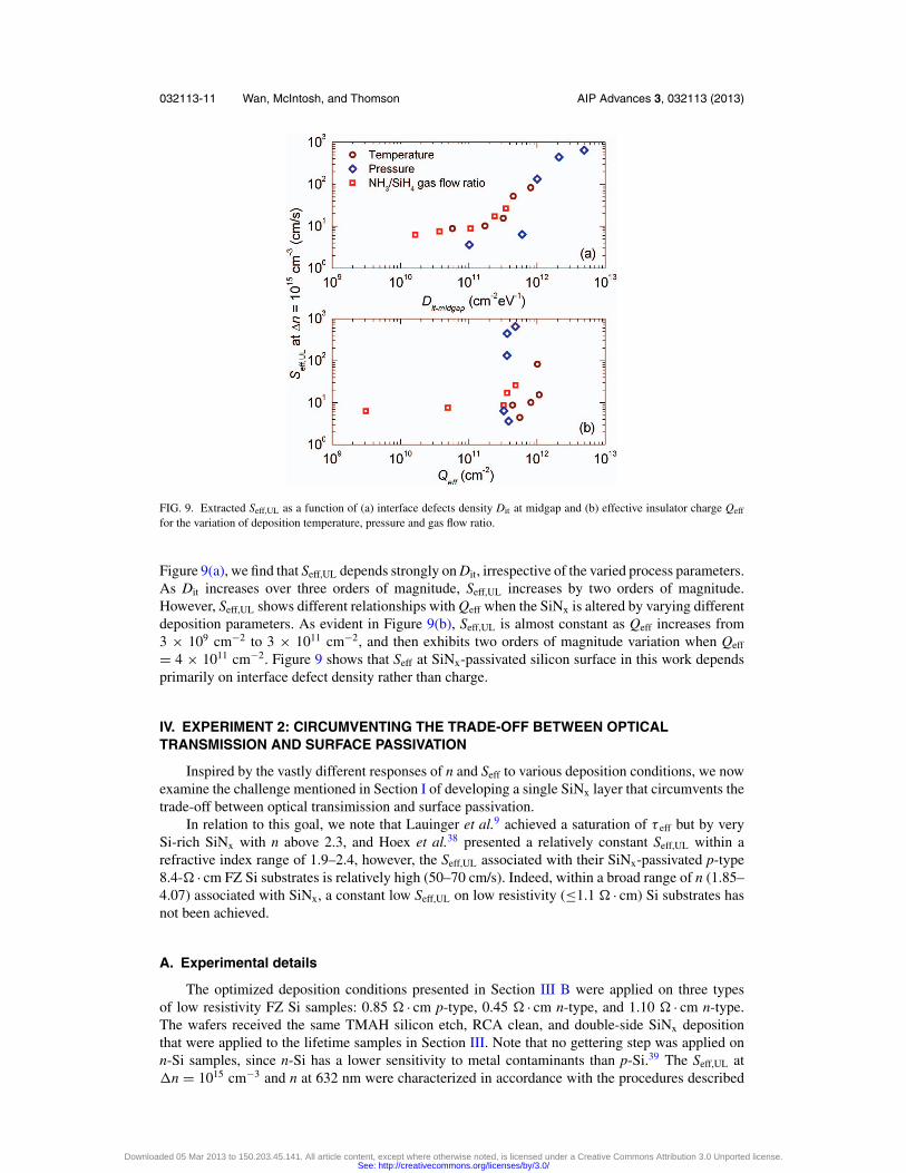
FIG. 9. Extracted Seff,UL as a function of (a) interface defects density Dit at midgap and (b) effective insulator charge Qeff
for the variation of deposition temperature, pressure and gas flow ratio.
Figure 9(a), we find that Seff,UL depends strongly on Dit, irrespective of the varied process parameters.As Dit increases over three orders of magnitude, Seff,UL increases by two orders of magnitude.However, Seff,UL shows different relationships with Qeff when the SiNx is altered by varying differentdeposition parameters. As evident in Figure 9(b), Seff,UL is almost constant as Qeff increases from3 × 109 cm−2 to 3 × 1011 cm−2, and then exhibits two orders of magnitude variation when Qeff
= 4 × 1011 cm−2. Figure 9 shows that Seff at SiNx-passivated silicon surface in this work dependsprimarily on interface defect density rather than charge.
IV. EXPERIMENT 2: CIRCUMVENTING THE TRADE-OFF BETWEEN OPTICALTRANSMISSION AND SURFACE PASSIVATION
Inspired by the vastly different responses of n and Seff to various deposition conditions, we nowexamine the challenge mentioned in Section I of developing a single SiNx layer that circumvents thetrade-off between optical transimission and surface passivation.
In relation to this goal, we note that Lauinger et al.9 achieved a saturation of τ eff but by verySi-rich SiNx with n above 2.3, and Hoex et al.38 presented a relatively constant Seff,UL within arefractive index range of 1.9–2.4, however, the Seff,UL associated with their SiNx-passivated p-type8.4-� · cm FZ Si substrates is relatively high (50–70 cm/s). Indeed, within a broad range of n (1.85–4.07) associated with SiNx, a constant low Seff,UL on low resistivity (≤1.1 � · cm) Si substrates hasnot been achieved.
A. Experimental details
The optimized deposition conditions presented in Section III B were applied on three typesof low resistivity FZ Si samples: 0.85 � · cm p-type, 0.45 � · cm n-type, and 1.10 � · cm n-type.The wafers received the same TMAH silicon etch, RCA clean, and double-side SiNx depositionthat were applied to the lifetime samples in Section III. Note that no gettering step was applied onn-Si samples, since n-Si has a lower sensitivity to metal contaminants than p-Si.39 The Seff,UL at�n = 1015 cm−3 and n at 632 nm were characterized in accordance with the procedures described
Downloaded 05 Mar 2013 to 150.203.45.141. All article content, except where otherwise noted, is licensed under a Creative Commons Attribution 3.0 Unported license.See: http://creativecommons.org/licenses/by/3.0/
032113-12 Wan, McIntosh, and Thomson AIP Advances 3, 032113 (2013)
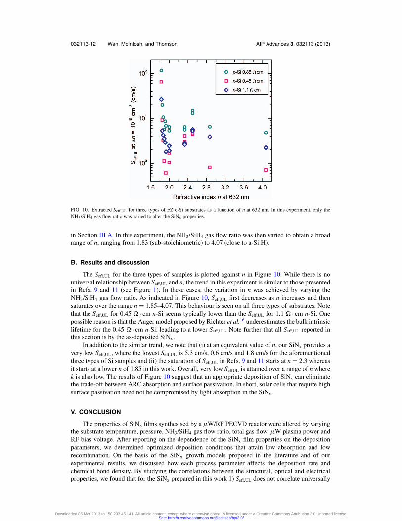
FIG. 10. Extracted Seff,UL for three types of FZ c-Si substrates as a function of n at 632 nm. In this experiment, only theNH3/SiH4 gas flow ratio was varied to alter the SiNx properties.
in Section III A. In this experiment, the NH3/SiH4 gas flow ratio was then varied to obtain a broadrange of n, ranging from 1.83 (sub-stoichiometric) to 4.07 (close to a-Si:H).
B. Results and discussion
The Seff,UL for the three types of samples is plotted against n in Figure 10. While there is nouniversal relationship between Seff,UL and n, the trend in this experiment is similar to those presentedin Refs. 9 and 11 (see Figure 1). In these cases, the variation in n was achieved by varying theNH3/SiH4 gas flow ratio. As indicated in Figure 10, Seff,UL first decreases as n increases and thensaturates over the range n = 1.85–4.07. This behaviour is seen on all three types of substrates. Notethat the Seff,UL for 0.45 � · cm n-Si seems typically lower than the Seff,UL for 1.1 � · cm n-Si. Onepossible reason is that the Auger model proposed by Richter et al.16 underestimates the bulk intrinsiclifetime for the 0.45 � · cm n-Si, leading to a lower Seff,UL. Note further that all Seff,UL reported inthis section is by the as-deposited SiNx.
In addition to the similar trend, we note that (i) at an equivalent value of n, our SiNx provides avery low Seff,UL, where the lowest Seff,UL is 5.3 cm/s, 0.6 cm/s and 1.8 cm/s for the aforementionedthree types of Si samples and (ii) the saturation of Seff,UL in Refs. 9 and 11 starts at n = 2.3 whereasit starts at a lower n of 1.85 in this work. Overall, very low SeffUL is attained over a range of n wherek is also low. The results of Figure 10 suggest that an appropriate deposition of SiNx can eliminatethe trade-off between ARC absorption and surface passivation. In short, solar cells that require highsurface passivation need not be compromised by light absorption in the SiNx.
V. CONCLUSION
The properties of SiNx films synthesised by a μW/RF PECVD reactor were altered by varyingthe substrate temperature, pressure, NH3/SiH4 gas flow ratio, total gas flow, μW plasma power andRF bias voltage. After reporting on the dependence of the SiNx film properties on the depositionparameters, we determined optimized deposition conditions that attain low absorption and lowrecombination. On the basis of the SiNx growth models proposed in the literature and of ourexperimental results, we discussed how each process parameter affects the deposition rate andchemical bond density. By studying the correlations between the structural, optical and electricalproperties, we found that for the SiNx prepared in this work 1) Seff,UL does not correlate universally
Downloaded 05 Mar 2013 to 150.203.45.141. All article content, except where otherwise noted, is licensed under a Creative Commons Attribution 3.0 Unported license.See: http://creativecommons.org/licenses/by/3.0/
032113-13 Wan, McIntosh, and Thomson AIP Advances 3, 032113 (2013)
with the bulk structural and optical properties such as chemical bond densities and refractive index,and 2) Seff,UL depends primarily on the defect density at the SiNx-Si interface rather than theinsulator charge. Finally, employing the optimized deposition condition, we achieved a relativelyconstant and low Seff,UL on low-resistivity (≤1.1 �cm) p- and n-type c-Si substrates over a broadrange of n = 1.85–4.07. The results demonstrate that the trade-off between optical transmissionand surface passivation can be circumvented by a judicious deposition of SiNx. Although we focuson photovoltaic applications, this study may be useful for any device for which it is desirable tomaximize light transmission and surface passivation.
ACKNOWLEDGMENT
The authors would like to thank Prof. Andres Cuevas and Dr. Saul Winderbaum for valuablediscussions. This work was supported by an Australian Research Council Linkage between TheAustralian National University and Braggone Oy under Grant LP0989593.
1 A. G. Aberle, Solar Energy Materials and Solar Cells 65, 239 (2001).2 C. Leguijt, P. Lolgen, J. A. Eikelboom, A. W. Weeber, F. M. Schuurmans, W. C. Sinke, P. F. A. Alkemade, P. M.
Sarro, C. H. M. Maree, and L. A. Verhoef, Solar Energy Materials and Solar Cells 40, 297 (1996).3 X. Dai and K. R. McIntosh, in Proc. 35th IEEE PVSC, Proc. 35th IEEE PVSC, 2010, pp. 3205.4 B. Gorowitz, T. B. Gorczyca, and R. J. Saia, Solid State Technology 28, 197 (1985).5 Z. Chen, A. Rohatgi, R. O. Bell, and J. P. Kalejs, Applied Physics Letters 65, 2078 (1994).6 A. W. Weeber, H. C. Rieffe, M. J. A. A. Goris, J. Hong, W. M. M. Kessels, M. C. M. van de Sanden, and W. J.
Soppe, in Photovoltaic Energy Conversion, 2003. Proceedings of 3rd World Conference on, 2003, p. 1131.7 H. F. W. Dekkers, L. Carnel, and G. Beaucarne, Applied Physics Letters 89, 013508 (2006).8 J. Hong, W. M. M. Kessels, W. J. Soppe, A. W. Weeber, W. M. Arnoldbik, and M. C. M. v. d. Sanden, Journal of
Vacuum Science & Technology B: Microelectronics and Nanometer Structures 21, 2123 (2003).9 T. Lauinger, J. Moschner, A. G. Aberle, and R. Hezel, Journal of Vacuum Science & Technology A: Vacuum, Surfaces,
and Films 16, 530 (1998).10 H. Mackel and R. Ludemann, Journal of Applied Physics 92, 2602 (2002).11 J. D. Moschner, J. Henze, J. Schmidt, and R. Hezel, Progress in Photovoltaics: Research and Applications 12, 21 (2004).12 J. F. Lelievre, E. Fourmond, A. Kaminski, O. Palais, D. Ballutaud, and M. Lemiti, Solar Energy Materials and Solar
Cells 93, 1281 (2009).13 S. D. Gupta, B. Hoex, L. Fen, T. Mueller, and A. G. Aberle, in Photovoltaic Specialists Conference (PVSC), 2011 37th
IEEE, 2011, p. 001421.14 J. Schmidt and M. Kerr, Solar Energy Materials and Solar Cells 65, 585 (2001).15 Y. Wan, K. R. McIntosh, A. F. Thomson, and A. Cuevas, Photovoltaics, IEEE Journal of PP, 1 (2012).16 A. Richter, S. W. Glunz, F. Werner, J. Schmidt, and A. Cuevas, Physical Review B 86, 165202 (2012).17 D. L. Smith, A. S. Alimonda, and F. J. v. Preissig, Journal of Vacuum Science & Technology B: Microelectronics and
Nanometer Structures 8, 551 (1990).18 W. M. M. Kessels, F. J. H. v. Assche, J. Hong, D. C. Schram, and M. C. M. v. d. Sanden, Journal of Vacuum Science
& Technology A: Vacuum, Surfaces, and Films 22, 96 (2004).19 P. J. v. d. Oever, J. H. v. Helden, J. L. v. Hemmen, R. Engeln, D. C. Schram, M. C. M. v. d. Sanden, and W. M. M.
Kessels, Journal of Applied Physics 100, 093303 (2006).20 S. P. Phang and D. Macdonald, Journal of Applied Physics 109, 073521 (2011).21 R. A. Sinton and A. Cuevas, Applied Physics Letters 69, 2510 (1996).22 F. Giorgis, F. Giuliani, C. F. Pirri, E. Tresso, C. Summonte, R. Rizzoli, R. Galloni, A. Desalvo, and P. Rava,
Philosophical Magazine Part B 77, 925 (1998).23 M. Cardona, physica status solidi (b) 118, 463 (1983).24 P. Doshi, G. E. Jellison, and A. Rohatgi, Appl. Opt. 36, 7826 (1997).25 S. Duttagupta, F. Ma, B. Hoex, T. Mueller, and A. G. Aberle, Energy Procedia 15, 78 (2012).26 M. H. Kang, K. Ryu, A. Upadhyaya, and A. Rohatgi, (John Wiley and Sons, Ltd.), p. n/a.27 A. G. Aberle, T. Lauinger, J. Schmidt, and R. Hezel, Applied Physics Letters 66, 2828 (1995).28 M. J. Kerr and A. Cuevas, Semiconductor Science and Technology 17, 166 (2002).29 J. R. Elmiger and M. Kunst, Applied Physics Letters 69, 517 (1996).30 G. Turban, Y. Catherine, and B. Grolleau, Thin Solid Films 67, 309 (1980).31 L. Martinu and D. Poitras, Journal of Vacuum Science & Technology A: Vacuum, Surfaces, and Films 18, 2619 (2000).32 J. Robertson, Philosophical Magazine Part B 63, 47 (1991).33 A. W. Weeber, H. C. Rieffe, I. G. Romijn, W. C. Sinke, and W. J. Soppe, in Photovoltaic Specialists Conference,
2005. Conference Record of the Thirty-first IEEE, 2005, p. 1043.34 A. Cuevas, C. Florence, T. Jason, M. Helmut, W. Saul, and R. Kristin, in Photovoltaic Energy Conversion, Conference
Record of the 2006 IEEE 4th World Conference on, 2006, p. 1148.
Downloaded 05 Mar 2013 to 150.203.45.141. All article content, except where otherwise noted, is licensed under a Creative Commons Attribution 3.0 Unported license.See: http://creativecommons.org/licenses/by/3.0/

032113-14 Wan, McIntosh, and Thomson AIP Advances 3, 032113 (2013)
35 F. Chen, I. Romijn, A. Weeber, J. Tan, B. Hallam, and J. Cotter, in 22nd European Photovoltaic Solar EnergyConference, Milan, Italy, 2007, p. 1053.
36 H. F. W. Dekkers, G. Beaucarne, M. Hiller, H. Charifi, and A. Slaoui, Applied Physics Letters 89, 211914 (2006).37 L. M. Terman, Solid-State Electronics 5, 285 (1962).38 B. Hoex, A. J. M. van Erven, R. C. M. Bosch, W. T. M. Stals, M. D. Bijker, P. J. van den Oever, W. M. M. Kessels,
and M. C. M. van de Sanden, Progress in Photovoltaics: Research and Applications 13, 705 (2005).39 D. Macdonald and L. J. Geerligs, Applied Physics Letters 85, 4061 (2004).
Downloaded 05 Mar 2013 to 150.203.45.141. All article content, except where otherwise noted, is licensed under a Creative Commons Attribution 3.0 Unported license.See: http://creativecommons.org/licenses/by/3.0/