Embed Size (px)
Citation preview
CK98 Clock Synthesizer/DriverDesign Guidelines
(Includes CK133 Definition)
November, 1999
Order Number: 245338-001
Information in this document is provided in connection with Intel products. No license, express or implied, by estoppel or otherwise, to anyintellectual property rights is granted by this document. Except as provided in Intel's Terms and Conditions of Sale for such products, Intelassumes no liability whatsoever, and Intel disclaims any express or implied warranty, relating to sale and/or use of Intel products includingliability or warranties relating to fitness for a particular purpose, merchantability, or infringement of any patent, copyright or other intellectualproperty right. Intel products are not intended for use in medical, life saving, or life sustaining applications.
The hardware vendor remains solely responsible for the design, sale and functionality of its product, including any liabilityarising from product infringement or product warranty, and Intel assumes no liability for vendor products, either alone or incombination with Intel products.
Intel may make changes to specifications and product descriptions at any time, without notice.
Designers must not rely on the absence or characteristics of any features or instructions marked "reserved" or "undefined." Intel reservesthese for future definition and shall have no responsibility whatsoever for conflicts or incompatibilities arising from future changes to them.
The Pentium® III processor, Pentium III Xeon processor and Intel® Celeron processor may contain design defects or errors known aserrata which may cause the product to deviate from published specifications. Current characterized errata are available on request.
Contact your local Intel sales office or your distributor to obtain the latest specifications and before placing your product order.
Copies of documents which have an ordering number and are referenced in this document, or other Intel literature, may be obtained bycalling 1-800-548-4725 or by visiting Intel’s website at http://www.intel.comCopyright © Intel Corporation 1999*
* Third-party brands and names are the property of their respective owners

CK98 Clock Synthesizer/Driver Design Guidelines
Page iv
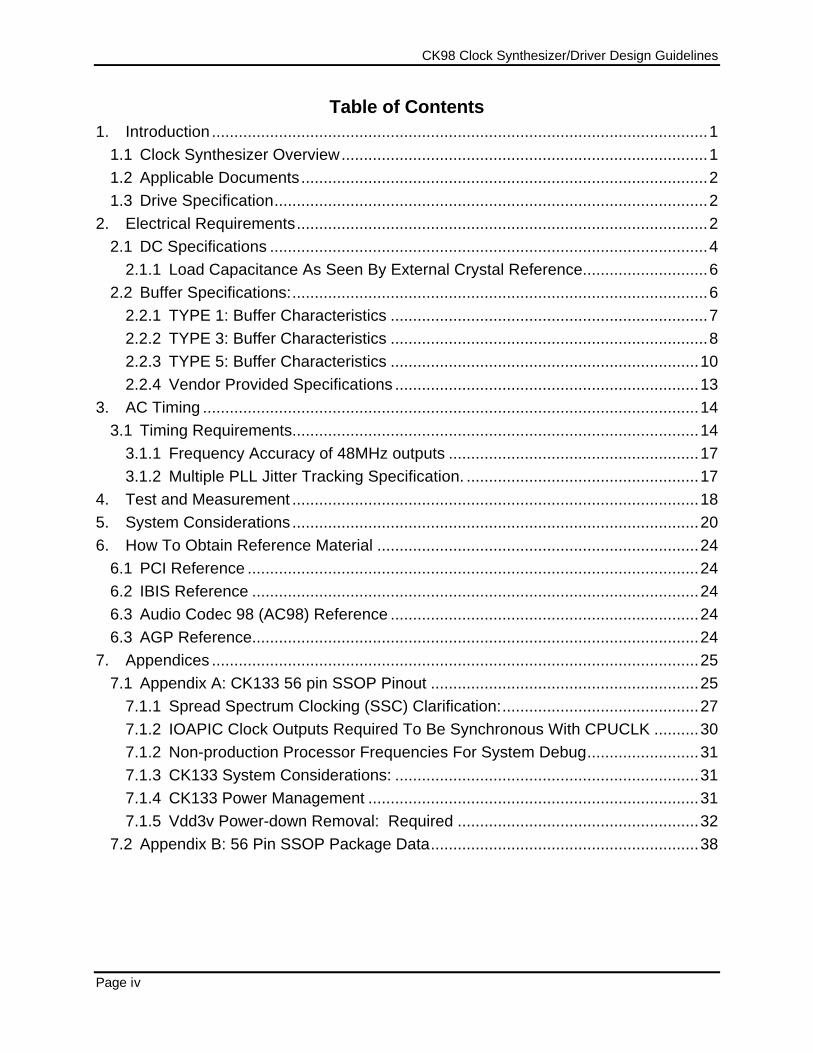
Table of Contents1. Introduction ...............................................................................................................1
1.1 Clock Synthesizer Overview..................................................................................11.2 Applicable Documents...........................................................................................21.3 Drive Specification.................................................................................................2
2. Electrical Requirements............................................................................................22.1 DC Specifications ..................................................................................................4
2.1.1 Load Capacitance As Seen By External Crystal Reference............................62.2 Buffer Specifications:.............................................................................................6
2.2.1 TYPE 1: Buffer Characteristics .......................................................................72.2.2 TYPE 3: Buffer Characteristics .......................................................................82.2.3 TYPE 5: Buffer Characteristics .....................................................................102.2.4 Vendor Provided Specifications ....................................................................13
3. AC Timing ...............................................................................................................143.1 Timing Requirements...........................................................................................14
3.1.1 Frequency Accuracy of 48MHz outputs ........................................................173.1.2 Multiple PLL Jitter Tracking Specification. ....................................................17
4. Test and Measurement ...........................................................................................185. System Considerations ...........................................................................................206. How To Obtain Reference Material ........................................................................24
6.1 PCI Reference .....................................................................................................246.2 IBIS Reference ....................................................................................................246.3 Audio Codec 98 (AC98) Reference .....................................................................246.3 AGP Reference....................................................................................................24
7. Appendices .............................................................................................................257.1 Appendix A: CK133 56 pin SSOP Pinout ............................................................25
7.1.1 Spread Spectrum Clocking (SSC) Clarification:............................................277.1.2 IOAPIC Clock Outputs Required To Be Synchronous With CPUCLK ..........307.1.2 Non-production Processor Frequencies For System Debug.........................317.1.3 CK133 System Considerations: ....................................................................317.1.4 CK133 Power Management ..........................................................................317.1.5 Vdd3v Power-down Removal: Required ......................................................32
7.2 Appendix B: 56 Pin SSOP Package Data............................................................38
CK98 Clock Synthesizer/Driver Design Guidelines
Revision 1.0 Page v
List of Figures
FIGURE 1 TYPE 1: PULL-UP CHARACTERISTICS................................................................................7FIGURE 2 TYPE 1: PULL-DOWN CHARACTERISTICS .........................................................................8FIGURE 3 TYPE 3: PULL-UP CHARACTERISTICS................................................................................9FIGURE 4 TYPE 3: PULL-DOWN CHARACTERISTICS .........................................................................9FIGURE 5 TYPE 5: PULL-UP CHARACTERISTICS.............................................................................. 10FIGURE 6 TYPE 5: PULL-DOWN CHARACTERISTICS ..................................................................... 12FIGURE 7 GROUP OFFSET WAVEFORMS......................................................................................... 16FIGURE 8 CK133 CLOCK WAVEFORMS............................................................................................. 19FIGURE 9 COMPONENT VERSUS SYSTEM MEASURE POINTS....................................................... 19FIGURE 10 TYPICAL CLOCK LAYOUT TOPOLOGIES ........................................................................ 20FIGURE 11 OVERSHOOT & UNDERSHOOT ...................................................................................... 23FIGURE 12 TRIANGULAR FREQUENCY MODULATION PROFILE. .................................................... 27FIGURE 13 SPECTRAL FUNDAMENTAL FREQUENCY COMPARISON ............................................. 28FIGURE 14 DOWNSTREAM PLL TRACKING SKEW AND MODULATION FREQUENCY.................... 29FIGURE 15 CK33 CPU_STOP# TIMING DIAGRAM.............................................................................. 35FIGURE 16 CK133 PCI_STOP# TIMING DIAGRAM ............................................................................. 36FIGURE 17 CK133 PWR_DWN# TIMING DIAGRAM............................................................................ 37
List of Tables
TABLE 1 ABSOLUTE MAXIMUM DC POWER SUPPLY .........................................................................4TABLE 2 ABSOLUTE MAXIMUM DC I/O.................................................................................................4TABLE 3 DC OPERATING REQUIREMENTS.........................................................................................5TABLE 4 BUFFER TYPES ......................................................................................................................6TABLE 5 TYPE 1: OPERATING REQUIREMENTS.................................................................................7TABLE 6 OPERATING REQUIREMENTS...............................................................................................8TABLE 7: OPERATING REQUIREMENTS............................................................................................ 10TABLE 8 HOST BUS AC TIMING REQUIREMENTS............................................................................. 14TABLE 9 GROUP SKEW AND JITTER LIMITS..................................................................................... 15TABLE 10 GROUP OFFSET LIMITS..................................................................................................... 15TABLE 11 MINIMUM AND MAXIMUM LUMPED CAPACITIVE TEST LOADS....................................... 18TABLE 12 LAYOUT DIMENSIONS........................................................................................................ 21TABLE 13 BOARD LEVEL SIMULATION CONDITIONS ....................................................................... 21TABLE 14 TYPICAL DC CHARACTERISTICS AT 3.3V CLOCK DESTINATION ................................... 22TABLE 15 AC SIGNAL QUALITY REQUIREMENTS AT DESTINATION............................................... 23TABLE 16 CK133 PIN DESCRIPTION TABLE ...................................................................................... 26TABLE 17 DESIRED PEAK AMPLITUDE REDUCTION BY SSC. ......................................................... 28TABLE 18 CK133 SELECT FUNCTIONS .............................................................................................. 30TABLE 19 CK133 TRUTH TABLE ......................................................................................................... 30TABLE 20 CK133 MAXIMUM ALLOWED CURRENT ............................................................................ 31TABLE 21 CK133 CLOCK ENABLE CONFIGURATION ........................................................................ 34TABLE 22 CK133 POWER MANAGEMENT REQUIREMENTS............................................................. 34

CK98 Clock Synthesizer/Driver Design Guidelines
Revision 1.0 Page 1
1. IntroductionThis document is designed to provide the industry with the technical specifications required byclock drivers and synthesizers to meet the needs of Intel architecture platforms. Split powersupply signaling to provide 2.5V and 3.3V clocks is a stated requirement for this class ofproducts. Additionally, the clocking solution must provide processor and chipset clockfrequencies of 133 MHz (7.50 nS period) and 100 MHz (10.00 nS period.)
This document is intended to aid clock circuit suppliers and computer OEMs in defining andusing the clock synthesizer components for all desktop system clocking requirements.
The 3.3V power supply is used to power the inputs, some of the outputs, all internal logic andthe PLL cores for the clock device. The 2.5V power supply is used to power the remainingoutputs for the clock device. Because the two power supplies are independent, and becausecurrent PC technology does not control the power sequencing for turning on or turning off thesystem, latch-up and potentially damaging conditions can exist during these power sequencingphases. Your design is required to operate properly and make no requirement of thesystem to sequence the power supplies.
This 2.5V signaling specification follows the JEDEC standard 8-X. It should be noted that thepreferred implementation of the 2.5V supply will be a 2.5V ±5% voltage regulator.Processor and chipset clock voltages above the specified +5% variation are not allowed.The 3.3V input signaling specification follows the JEDEC standard for LVTTL signaling. The3.3V power delivery specification follows the JEDEC standard range 3.3V ±5%.
This document provides a baseline of development for future Intel Architecture processor-based platform clock driver requirements. It is not the only implementation that can bedeveloped; however, this baseline functionality is required for most desktop platforms.
1.1 Clock Synthesizer OverviewClock synthesizers are expected to source multiple clock types: e.g. Host clock, PCI clock andothers as defined by IA system requirements. This document deals with the processor clock,other Host bus clocks, PCI clocks, IOAPIC clocks, 48MHz, and copies of the reference clock.This class of products will also be required to generate fixed frequency 66 MHz outputs.
There are no references to the number of clocks or the types of clocks any given clock driverchip will supply in the main body of the document. Examples of clock synthesizer designs arelocated in the appendix. The number of clocks and types of outputs, package type and loadconditions are also defined.
CK98 Clock Synthesizer/Driver Design Guidelines
Page 2
1.2 Applicable DocumentsThe latest revision of the following are used as reference documents:
JEDEC Standard No. 8-1A, Interface Standard for 3.3±0.3 V Power Supply & Digital Integrated Circuits.JEDEC Standard No. 8-X, 2.5V±0.2V (normal range), and 1.8V to 2.7V (wide range) Power supplyVoltage and Interface Standard for Non-terminated Digital Integrated Circuit.PCI Specification 2.1IBIS Modeling SpecificationAudio Codec 98 Specification (AC98)AGP specification
Other Intel Clock Specification Documents:CK97 Clock Design Guidelines
See section 6 on how to obtain copies of PCI, AC98, AGP and IBIS specifications.
1.3 Drive SpecificationThe primary motivation for this document is to specify the issues associated with split I/Ovoltage and the effects of it on system power delivery, signaling, timing and test. Thesignaling, timing, and test characteristics change with the different supply voltages and need tobe thoroughly understood and simulated for optimal system performance.
The clock driver output buffers are specified in terms of the AC switching characteristics andtheir DC drive characteristics. The primary electrical parameters are the voltage to currentrelationship (V/I), and rise and fall time (Trise/Tfall) of the driver through its active switchingrange.
2. Electrical RequirementsThis section details the electrical parameters for two types of 2.5V clock output buffers,multiple types of 3.3V clock output buffers and a 5.0V compatible 3.3V PCI clock driver outputbuffer. The different types of 2.5V and 3.3V drivers are needed to compensate forcorresponding board layout topologies.
Due to the low voltage (<3.0V) required by the CPU, TTL output signaling levels are no longerviable. A signaling level to support 2.5V is being used for that portion of the design. TheJEDEC standard called “2.5V±0.2V (normal range), and 1.8V to 2.7V (wide range) PowerSupply Voltage and Interface Standard for Non-terminated Digital Integrated Circuit”, hereafterreferred to as 2.5V signaling and 2.5V supply is being used. The 3.3V clocking requirementsstill support the TTL-level compatible requirements and will be called by their appropriatename, LVTTL, even though they are TTL signaling levels.
A clock driver designed to operate in the 2.5V Pentium and Pentium III Processor signalingenvironment will not necessarily operate correctly in the 3.3V LVTTL or the 5.0V PCI I/O bussignaling environment. Great care must be taken in this design environment to properlysupport the extremely tight timing requirements between clocks.
CK98 Clock Synthesizer/Driver Design Guidelines
Revision 1.0 Page 3
The clock driver for all clocks must generate monotonic edges through the input thresholdregions as specified for each signaling environment. Many conditions exist in the design of theclock driver and the system that can affect the monotonic operation of the clock driver. Powersupply noise, pin inductance and capacitance, ratio of clock signals to Vddq and Vss pins, androuting topology will affect the monotonicity of these clocks. The electrical requirementsoutlined here ensure components connect directly together without any external buffers orother "glue" logic. Series terminating resistors may be required to keep noise within limits onstrong drivers under lightly loaded conditions. Components should be designed to operatewithin the "commercial" range of environmental parameters. However, this does not precludethe option of other operating environments at the vendor's discretion.
Clock driver output buffers are specified in terms of their V/I curves and Trise/Tfall times.Limits on acceptable V/I curves provide for a maximum output impedance that can achieveacceptable timing in typical configurations, and for a minimum output impedance that keepsthe reflected wave within reasonable bounds for signal quality. It is important to understandthat drive strength and layout topology go hand in hand. Point-to-point or multiple stubs at thereceiver end will work with a weaker driver, whereas a route that splits at the driver requires astronger buffer. The signal quality problems of a strong driver under light loads can benegated somewhat with a series termination resistor placed as close to the driver as possible.See Section 5 for more detail.
Examples of possible clock driver designs are contained in the appendices. These are not theonly solutions that can be achieved, but are a good starting point to design a component tomeet specific design requirements.
Due to the mixed power supplies now required for proper system operation, it is veryimportant to understand that specific power supply sequencing is not supported. Theclock synthesizer CANNOT force power sequencing requirements in the system.
CK98 Clock Synthesizer/Driver Design Guidelines
Page 4
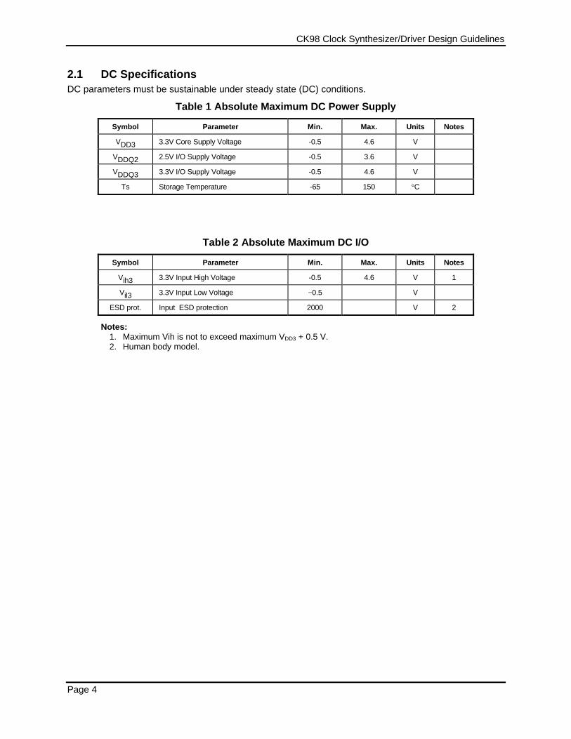
2.1 DC SpecificationsDC parameters must be sustainable under steady state (DC) conditions.
Table 1 Absolute Maximum DC Power Supply
Symbol Parameter Min. Max. Units Notes
VDD3 3.3V Core Supply Voltage -0.5 4.6 V
VDDQ2 2.5V I/O Supply Voltage -0.5 3.6 V
VDDQ3 3.3V I/O Supply Voltage -0.5 4.6 V
Ts Storage Temperature -65 150 °C
Table 2 Absolute Maximum DC I/O
Symbol Parameter Min. Max. Units Notes
Vih3 3.3V Input High Voltage -0.5 4.6 V 1
Vil3 3.3V Input Low Voltage −0.5 V
ESD prot. Input ESD protection 2000 V 2
Notes:1. Maximum Vih is not to exceed maximum VDD3 + 0.5 V.2. Human body model.
CK98 Clock Synthesizer/Driver Design Guidelines
Revision 1.0 Page 5
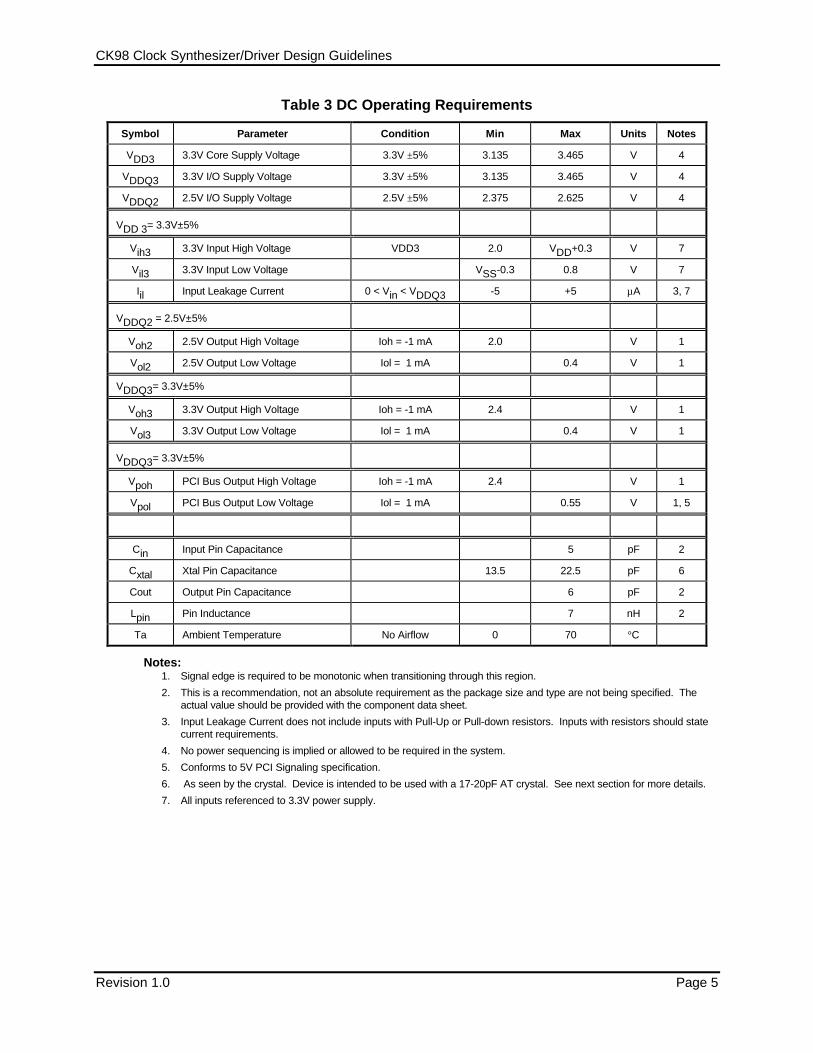
Table 3 DC Operating Requirements
Symbol Parameter Condition Min Max Units Notes
VDD3 3.3V Core Supply Voltage 3.3V ±5% 3.135 3.465 V 4
VDDQ3 3.3V I/O Supply Voltage 3.3V ±5% 3.135 3.465 V 4
VDDQ2 2.5V I/O Supply Voltage 2.5V ±5% 2.375 2.625 V 4
VDD 3= 3.3V±5%
Vih3 3.3V Input High Voltage VDD3 2.0 VDD+0.3 V 7
Vil3 3.3V Input Low Voltage VSS-0.3 0.8 V 7
Iil Input Leakage Current 0 < Vin < VDDQ3 -5 +5 µA 3, 7
VDDQ2 = 2.5V±5%
Voh2 2.5V Output High Voltage Ioh = -1 mA 2.0 V 1
Vol2 2.5V Output Low Voltage Iol = 1 mA 0.4 V 1
VDDQ3= 3.3V±5%
Voh3 3.3V Output High Voltage Ioh = -1 mA 2.4 V 1
Vol3 3.3V Output Low Voltage Iol = 1 mA 0.4 V 1
VDDQ3= 3.3V±5%
Vpoh PCI Bus Output High Voltage Ioh = -1 mA 2.4 V 1
Vpol PCI Bus Output Low Voltage Iol = 1 mA 0.55 V 1, 5
Cin Input Pin Capacitance 5 pF 2
Cxtal Xtal Pin Capacitance 13.5 22.5 pF 6
Cout Output Pin Capacitance 6 pF 2
Lpin Pin Inductance 7 nH 2
Ta Ambient Temperature No Airflow 0 70 °C
Notes:1. Signal edge is required to be monotonic when transitioning through this region.
2. This is a recommendation, not an absolute requirement as the package size and type are not being specified. Theactual value should be provided with the component data sheet.
3. Input Leakage Current does not include inputs with Pull-Up or Pull-down resistors. Inputs with resistors should statecurrent requirements.
4. No power sequencing is implied or allowed to be required in the system.
5. Conforms to 5V PCI Signaling specification.
6. As seen by the crystal. Device is intended to be used with a 17-20pF AT crystal. See next section for more details.
7. All inputs referenced to 3.3V power supply.
CK98 Clock Synthesizer/Driver Design Guidelines
Page 6
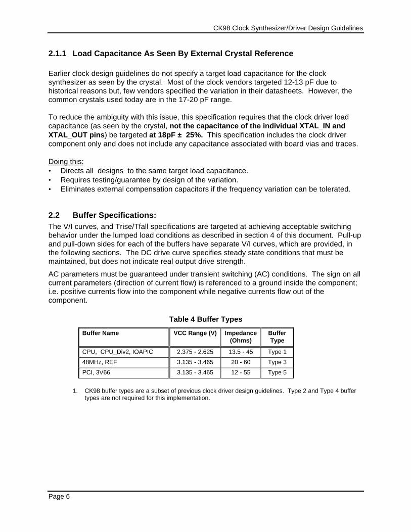
2.1.1 Load Capacitance As Seen By External Crystal Reference
Earlier clock design guidelines do not specify a target load capacitance for the clocksynthesizer as seen by the crystal. Most of the clock vendors targeted 12-13 pF due tohistorical reasons but, few vendors specified the variation in their datasheets. However, thecommon crystals used today are in the 17-20 pF range.
To reduce the ambiguity with this issue, this specification requires that the clock driver loadcapacitance (as seen by the crystal, not the capacitance of the individual XTAL_IN andXTAL_OUT pins) be targeted at 18pF ± 25%. This specification includes the clock drivercomponent only and does not include any capacitance associated with board vias and traces.
Doing this:• Directs all designs to the same target load capacitance.• Requires testing/guarantee by design of the variation.• Eliminates external compensation capacitors if the frequency variation can be tolerated.
2.2 Buffer Specifications:The V/I curves, and Trise/Tfall specifications are targeted at achieving acceptable switchingbehavior under the lumped load conditions as described in section 4 of this document. Pull-upand pull-down sides for each of the buffers have separate V/I curves, which are provided, inthe following sections. The DC drive curve specifies steady state conditions that must bemaintained, but does not indicate real output drive strength.
AC parameters must be guaranteed under transient switching (AC) conditions. The sign on allcurrent parameters (direction of current flow) is referenced to a ground inside the component;i.e. positive currents flow into the component while negative currents flow out of thecomponent.
Table 4 Buffer Types
Buffer Name VCC Range (V) Impedance(Ohms)
BufferType
CPU, CPU_Div2, IOAPIC 2.375 - 2.625 13.5 - 45 Type 1
48MHz, REF 3.135 - 3.465 20 - 60 Type 3
PCI, 3V66 3.135 - 3.465 12 - 55 Type 5
1. CK98 buffer types are a subset of previous clock driver design guidelines. Type 2 and Type 4 buffertypes are not required for this implementation.
CK98 Clock Synthesizer/Driver Design Guidelines
Revision 1.0 Page 7
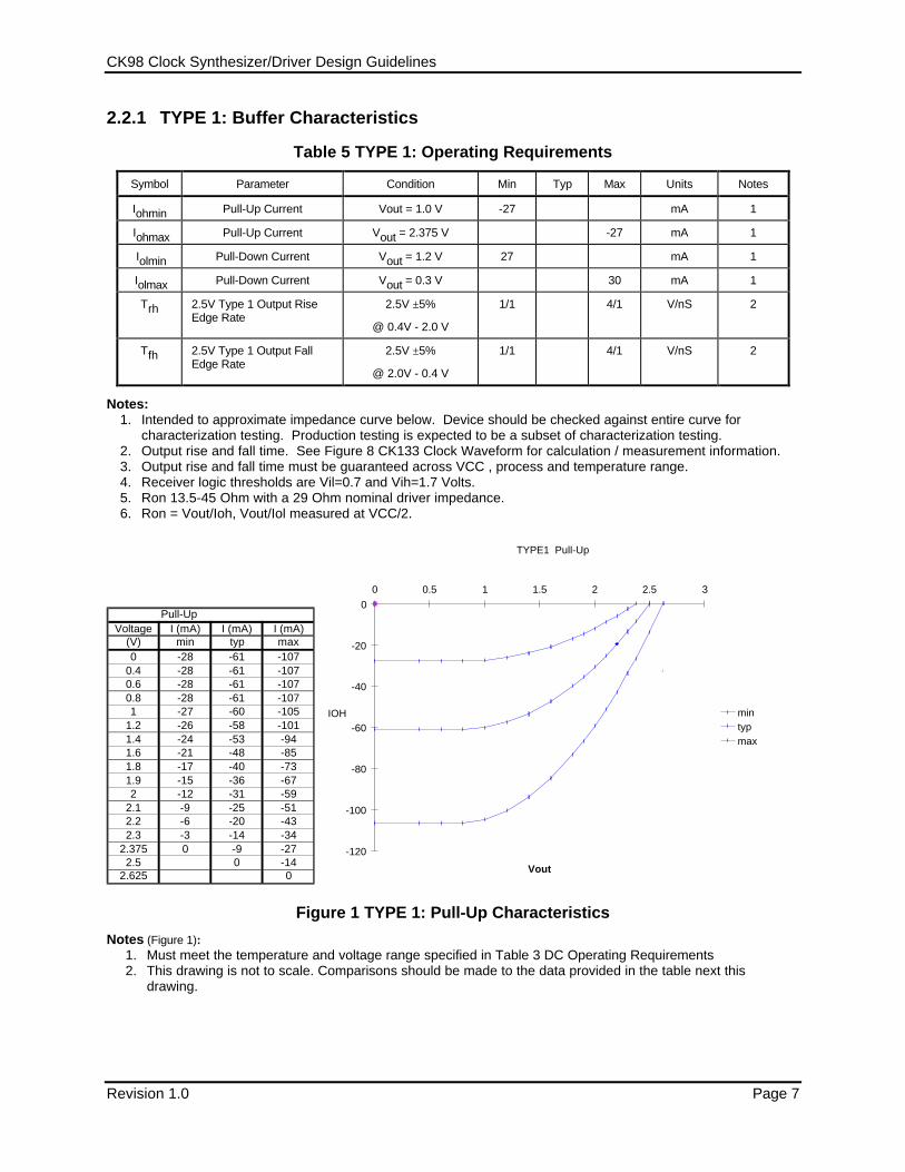
2.2.1 TYPE 1: Buffer Characteristics
Table 5 TYPE 1: Operating Requirements
Symbol Parameter Condition Min Typ Max Units Notes
Iohmin Pull-Up Current Vout = 1.0 V -27 mA 1
Iohmax Pull-Up Current Vout = 2.375 V -27 mA 1
Iolmin Pull-Down Current Vout = 1.2 V 27 mA 1
Iolmax Pull-Down Current Vout = 0.3 V 30 mA 1
Trh 2.5V Type 1 Output RiseEdge Rate
2.5V ±5%
@ 0.4V - 2.0 V
1/1 4/1 V/nS 2
Tfh 2.5V Type 1 Output FallEdge Rate
2.5V ±5%
@ 2.0V - 0.4 V
1/1 4/1 V/nS 2
Notes:1. Intended to approximate impedance curve below. Device should be checked against entire curve for
characterization testing. Production testing is expected to be a subset of characterization testing.2. Output rise and fall time. See Figure 8 CK133 Clock Waveform for calculation / measurement information.3. Output rise and fall time must be guaranteed across VCC , process and temperature range.4. Receiver logic thresholds are Vil=0.7 and Vih=1.7 Volts.5. Ron 13.5-45 Ohm with a 29 Ohm nominal driver impedance.6. Ron = Vout/Ioh, Vout/Iol measured at VCC/2.
Pull-UpVoltage I (mA) I (mA) I (mA)
(V) min typ max0 -28 -61 -107
0.4 -28 -61 -1070.6 -28 -61 -1070.8 -28 -61 -1071 -27 -60 -105
1.2 -26 -58 -1011.4 -24 -53 -941.6 -21 -48 -851.8 -17 -40 -731.9 -15 -36 -672 -12 -31 -59
2.1 -9 -25 -512.2 -6 -20 -432.3 -3 -14 -34
2.375 0 -9 -272.5 0 -14
2.625 0
TYPE1 Pull-Up
-120
-100
-80
-60
-40
-20
0
0 0.5 1 1.5 2 2.5 3
Vout
IOH mintypmax
Figure 1 TYPE 1: Pull-Up Characteristics
Notes (Figure 1):1. Must meet the temperature and voltage range specified in Table 3 DC Operating Requirements2. This drawing is not to scale. Comparisons should be made to the data provided in the table next this
drawing.
CK98 Clock Synthesizer/Driver Design Guidelines
Page 8
Pull-DownVoltage I (mA) I (mA) I (mA)
(V) min typ max0 0 0 0
0.1 3 7 110.2 6 13 210.3 9 19 300.4 12 24 400.5 15 30 480.6 17 35 560.7 19 39 630.8 21 43 700.9 23 47 771 24 50 83
1.1 25 53 881.2 27 56 931.3 27 58 971.4 28 60 1001.6 29 62 1061.8 29 63 1102 29 63 111
2.2 29 63 1112.375 29 63 1112.5 63 111
2.625 111
Type 1 Pull-Down
0
20
40
60
80
100
120
0 0.5 1 1.5 2 2.5 3
Vout
IOL
mintypmax
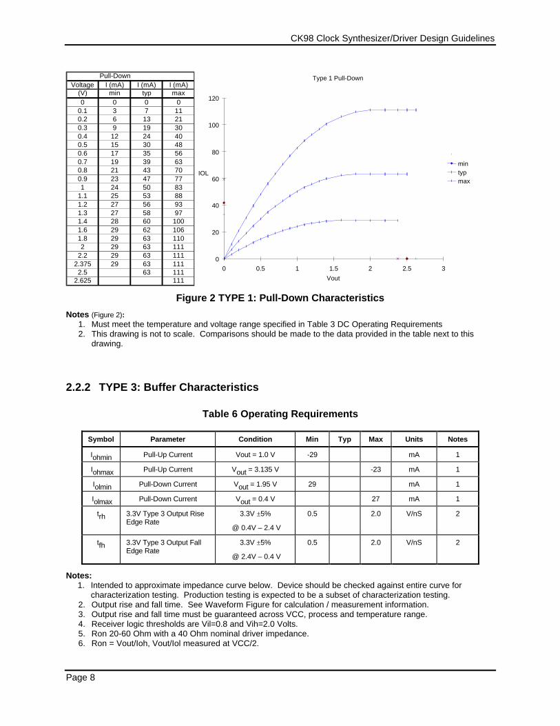
Figure 2 TYPE 1: Pull-Down Characteristics
Notes (Figure 2):1. Must meet the temperature and voltage range specified in Table 3 DC Operating Requirements2. This drawing is not to scale. Comparisons should be made to the data provided in the table next to this
drawing.
2.2.2 TYPE 3: Buffer Characteristics
Table 6 Operating Requirements
Symbol Parameter Condition Min Typ Max Units Notes
Iohmin Pull-Up Current Vout = 1.0 V -29 mA 1
Iohmax Pull-Up Current Vout = 3.135 V -23 mA 1
Iolmin Pull-Down Current Vout = 1.95 V 29 mA 1
Iolmax Pull-Down Current Vout = 0.4 V 27 mA 1
trh 3.3V Type 3 Output RiseEdge Rate
3.3V ±5%
@ 0.4V – 2.4 V
0.5 2.0 V/nS 2
tfh 3.3V Type 3 Output FallEdge Rate
3.3V ±5%
@ 2.4V – 0.4 V
0.5 2.0 V/nS 2
Notes:1. Intended to approximate impedance curve below. Device should be checked against entire curve for
characterization testing. Production testing is expected to be a subset of characterization testing.2. Output rise and fall time. See Waveform Figure for calculation / measurement information.3. Output rise and fall time must be guaranteed across VCC, process and temperature range.4. Receiver logic thresholds are Vil=0.8 and Vih=2.0 Volts.5. Ron 20-60 Ohm with a 40 Ohm nominal driver impedance.6. Ron = Vout/Ioh, Vout/Iol measured at VCC/2.
CK98 Clock Synthesizer/Driver Design Guidelines
Revision 1.0 Page 9
Pull-UpVoltage I (mA) I (mA) I (mA)
(V) min typ max0 -29 -46 -991 -29 -46 -99
1.4 -27 -44 -941.5 -27 -43 -921.65 -25 -41 -891.8 -24 -39 -852 -22 -36 -79
2.4 -16 -28 -632.6 -12 -22 -53
3.135 0 -6 -233.3 0 -12
3.465 0
Type3 Pull-Up
-120
-100
-80
-60
-40
-20
0
0 0.5 1 1.5 2 2.5 3 3.5
Vout
IOH mintypmax
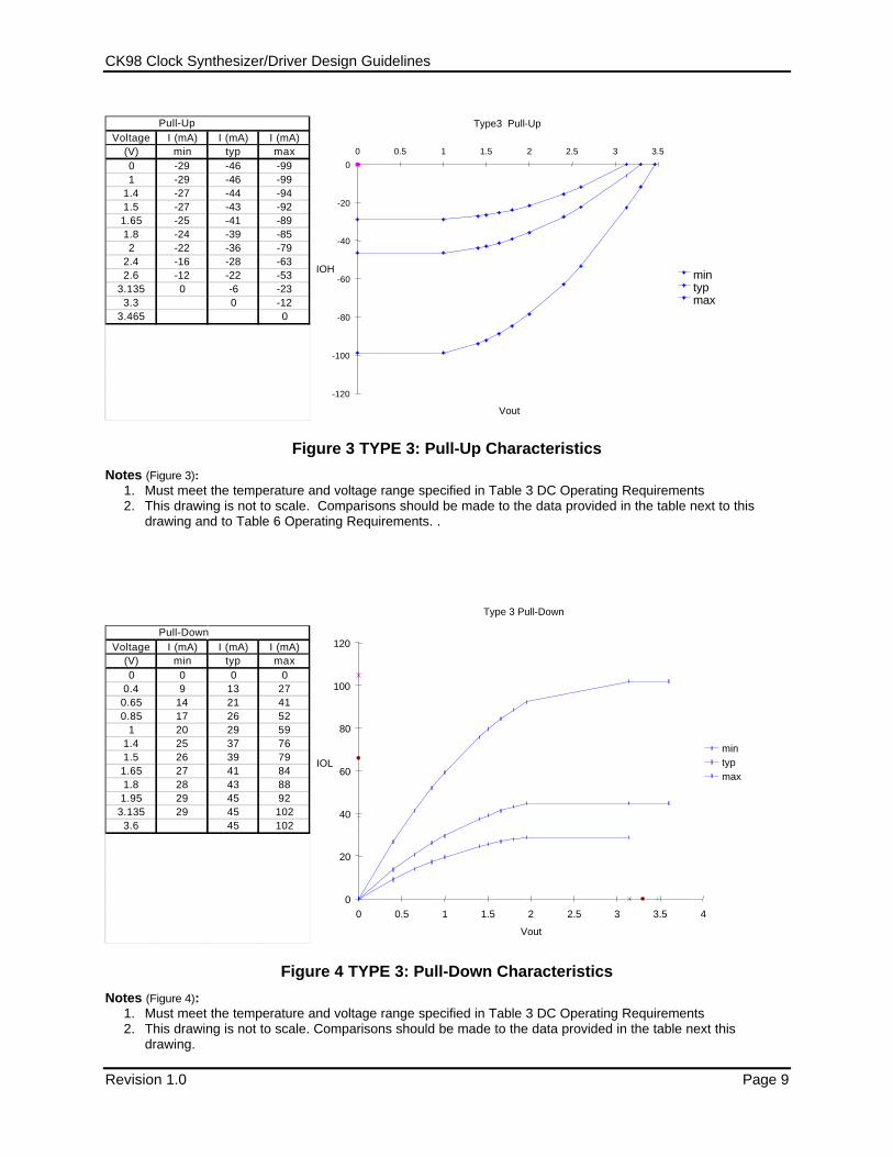
Figure 3 TYPE 3: Pull-Up Characteristics
Notes (Figure 3):1. Must meet the temperature and voltage range specified in Table 3 DC Operating Requirements2. This drawing is not to scale. Comparisons should be made to the data provided in the table next to this
drawing and to Table 6 Operating Requirements. .
Pull-DownVoltage I (mA) I (mA) I (mA)
(V) min typ max0 0 0 0
0.4 9 13 270.65 14 21 410.85 17 26 52
1 20 29 591.4 25 37 761.5 26 39 791.65 27 41 841.8 28 43 881.95 29 45 92
3.135 29 45 1023.6 45 102
Type 3 Pull-Down
0
20
40
60
80
100
120
0 0.5 1 1.5 2 2.5 3 3.5 4
Vout
IOL
mintypmax
Figure 4 TYPE 3: Pull-Down Characteristics
Notes (Figure 4):1. Must meet the temperature and voltage range specified in Table 3 DC Operating Requirements2. This drawing is not to scale. Comparisons should be made to the data provided in the table next this
drawing.
CK98 Clock Synthesizer/Driver Design Guidelines
Page 10
2.2.3 TYPE 5: Buffer Characteristics
Table 7: Operating Requirements
Symbol Parameter Condition Min Typ Max Units Notes
Iohmin Pull-Up Current Vout = 1.0 V -33 mA 1
Iohmax Pull-Up Current Vout = 3.135 V -33 mA 1
Iolmin Pull-Down Current Vout = 1.95 V 30 mA 1
Iolmax Pull-Down Current Vout = 0.4 V 38 mA 1
Trh 3.3V Type 4 Output RiseEdge Rate
3.3V ±5%
@ 0.4V - 2.4 V
1/1 4/1 V/nS 2
Tfh 3.3V Type 4 Output FallEdge Rate
3.3V ±5%
@ 2.4V - 0.4 V
1/1 4/1 V/nS 2
Notes:1. Intended to approximate impedance curve below. Device should be checked against entire curve for characterization testing.
Production testing is expected to be a subset of characterization testing.2. Output rise and fall time. See Figure 8 CK133 Clock Waveform for calculation / measurement information.3. Output rise and fall time must be guaranteed across VCC , process and temperature range.4. Receiver logic thresholds are Vil=0.8 and Vih=2.0 Volts.5. Ron 12-55 Ohm with a 30 Ohm nominal driver impedance.6. Ron = Vout/Ioh, Vout/Iol measured at VCC/2.7. See PCI specification for additional PCI details.
Pull-UpVoltage I (mA) I (mA) I (mA)
(V) min typ max0 -34 -59 -1951 -33 -58 -194
1.4 -31 -55 -1891.5 -30 -54 -184
1.65 -28 -52 -1721.8 -25.5 -50 -159
2 -22 -46 -1402.4 -14.5 -35 -1002.6 -11 -28 -83
3.135 0 -6 -333.3 0 -193.6 0
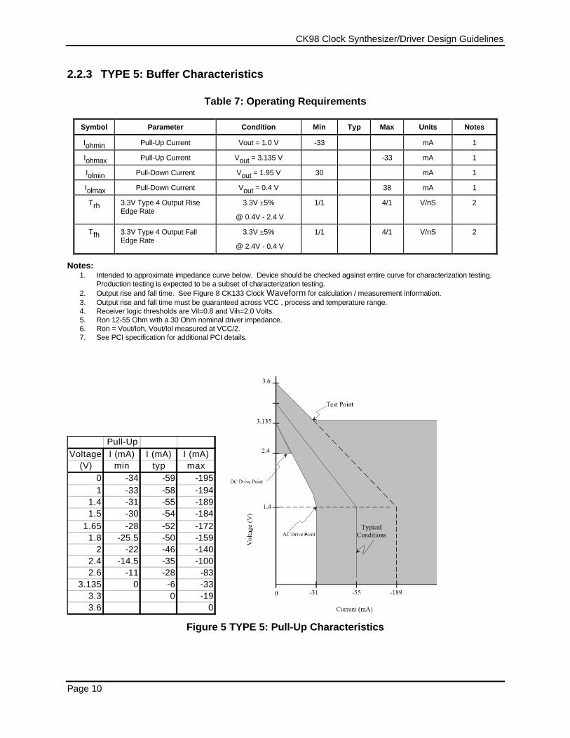
Figure 5 TYPE 5: Pull-Up Characteristics
CK98 Clock Synthesizer/Driver Design Guidelines
Revision 1.0 Page 11
Notes (Figure 5):1. Must meet the temperature and voltage range specified in Table 3 DC Operating Requirements.2. This drawing is not to scale. Comparisons should be made to the data provided in the table next to it and to Table 7: Operating
Requirements
CK98 Clock Synthesizer/Driver Design Guidelines
Page 12
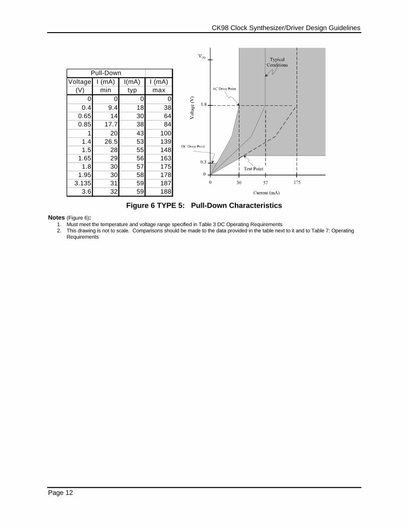
Pull-DownVoltage I (mA) I(mA) I (mA)
(V) min typ max0 0 0 0
0.4 9.4 18 380.65 14 30 640.85 17.7 38 84
1 20 43 1001.4 26.5 53 1391.5 28 55 148
1.65 29 56 1631.8 30 57 175
1.95 30 58 1783.135 31 59 187
3.6 32 59 188
Figure 6 TYPE 5: Pull-Down Characteristics
Notes (Figure 6):1. Must meet the temperature and voltage range specified in Table 3 DC Operating Requirements2. This drawing is not to scale. Comparisons should be made to the data provided in the table next to it and to Table 7: Operating
Requirements
CK98 Clock Synthesizer/Driver Design Guidelines
Revision 1.0 Page 13
2.2.4 Vendor Provided Specifications
Vendors should make the following information available in their data sheets:
• Pin capacitance for all pins (min and max).
• Pin inductance for all pins (min and max).
• Output V/I curves under switching conditions. Two graphs/tables should be given foreach output type used: one for driving high, the other for driving low. Both should showbest and worst case conditions.
• Loaded rise/fall times for each output type for loads as specified in the test section ofthis document.
• Absolute maximum data, including operating and non-operating temperature, DCmaximums, etc.
It is strongly recommended that component vendors make the following informationelectronically available in the IBIS model format. Include the following minimum information:
• Output V/I curves under switching conditions. Two curves should be supplied one fordriving high, the other for driving low. Both should show best-typical-worst curves.
• Unloaded rise/fall times for each output type as specified by IBIS.
• Package Resistance (R_pkg [min, max]), Package Inductance (L_pkg [min, max]),Package Capacitance (C_pkg [min, max]); Component Capacitance (C_comp [min,max]).
CK98 Clock Synthesizer/Driver Design Guidelines
Page 14
3. AC Timing
3.1 Timing Requirements
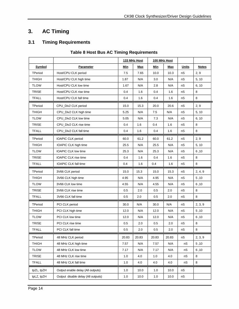
Table 8 Host Bus AC Timing Requirements
133 MHz Host 100 MHz Host
Symbol Parameter Min Max Min Max Units Notes
TPeriod Host/CPU CLK period 7.5 7.65 10.0 10.3 nS 2, 9
THIGH Host/CPU CLK high time 1.87 N/A 3.0 N/A nS 5, 10
TLOW Host/CPU CLK low time 1.67 N/A 2.8 N/A nS 6, 10
TRISE Host/CPU CLK rise time 0.4 1.6 0.4 1.6 nS 8
TFALL Host/CPU CLK fall time 0.4 1.6 0.4 1.6 nS 8
TPeriod CPU_Div2 CLK period 15.0 15.3 20.0 20.6 nS 2, 9
THIGH CPU_Div2 CLK high time 5.25 N/A 7.5 N/A nS 5, 10
TLOW CPU_Div2 CLK low time 5.05 N/A 7.3 N/A nS 6, 10
TRISE CPU_Div2 CLK rise time 0.4 1.6 0.4 1.6 nS 8
TFALL CPU_Div2 CLK fall time 0.4 1.6 0.4 1.6 nS 8
TPeriod IOAPIC CLK period 60.0 61.2 60.0 61.2 nS 2, 9
THIGH IOAPIC CLK high time 25.5 N/A 25.5 N/A nS 5, 10
TLOW IOAPIC CLK low time 25.3 N/A 25.3 N/A nS 6 ,10
TRISE IOAPIC CLK rise time 0.4 1.6 0.4 1.6 nS 8
TFALL IOAPIC CLK fall time 0.4 1.6 0.4 1.6 nS 8
TPeriod 3V66 CLK period 15.0 15.3 15.0 15.3 nS 2, 4, 9
THIGH 3V66 CLK high time 4.95 N/A 4.95 N/A nS 5 ,10
TLOW 3V66 CLK low time 4.55 N/A 4.55 N/A nS 6 ,10
TRISE 3V66 CLK rise time 0.5 2.0 0.5 2.0 nS 8
TFALL 3V66 CLK fall time 0.5 2.0 0.5 2.0 nS 8
TPeriod PCI CLK period 30.0 N/A 30.0 N/A nS 2, 3, 9
THIGH PCI CLK high time 12.0 N/A 12.0 N/A nS 5 ,10
TLOW PCI CLK low time 12.0 N/A 12.0 N/A nS 6 ,10
TRISE PCI CLK rise time 0.5 2.0 0.5 2.0 nS 8
TFALL PCI CLK fall time 0.5 2.0 0.5 2.0 nS 8
TPeriod 48 MHz CLK period 20.83 20.83 20.83 20.83 nS 2, 3, 9
THIGH 48 MHz CLK high time 7.57 N/A 7.57 N/A nS 5 ,10
TLOW 48 MHz CLK low time 7.17 N/A 7.17 N/A nS 6 ,10
TRISE 48 MHz CLK rise time 1.0 4.0 1.0 4.0 nS 8
TFALL 48 MHz CLK fall time 1.0 4.0 4.0 4.0 nS 8
tpZL, tpZH Output enable delay (All outputs) 1.0 10.0 1.0 10.0 nS
tpLZ, tpZH Output disable delay (All outputs) 1.0 10.0 1.0 10.0 nS
CK98 Clock Synthesizer/Driver Design Guidelines
Revision 1.0 Page 15
tstable All clock Stabilization from power-up 3 3 mS 7
Notes: 1. Output drivers must have monotonic rise/fall times through the specified VOL/VOH levels.2. Period, jitter, offset and skew measured on rising edge @1.25V for 2.5V clocks and @ 1.5V for 3.3V clocks.3. The PCI clock is the Host clock divided by four at Host=133MHz. PCI clock is the Host clock divided by
three at Host = 100MHz.4. 3V66 is internal VCO frequency divided by four for Host=133MHz. 3V66 clock is internal VCO frequency
divided by three for Host=100MHz5. THIGH is measured at 2.0V for 2.5V outputs, 2.4V for 3.3V outputs.6. TLOW is measured at 0.4V for all outputs.7. The time specified is measured from when Vddq achieves its nominal operating level (typical condition Vddq
= 3.3V) till the frequency output is stable and operating within specification.8. TRISE and TFALL are measured as a transition through the threshold region VOL and VOH.9. The average period over any 1 uS period of time must be greater than the minimum specified period10. Calculated at minimum edge-rate (1V/nS) to guarantee 45/55% duty-cycle. Pulse width is required to be
wider at faster edge-rate to ensure duty-cycle specification is met.
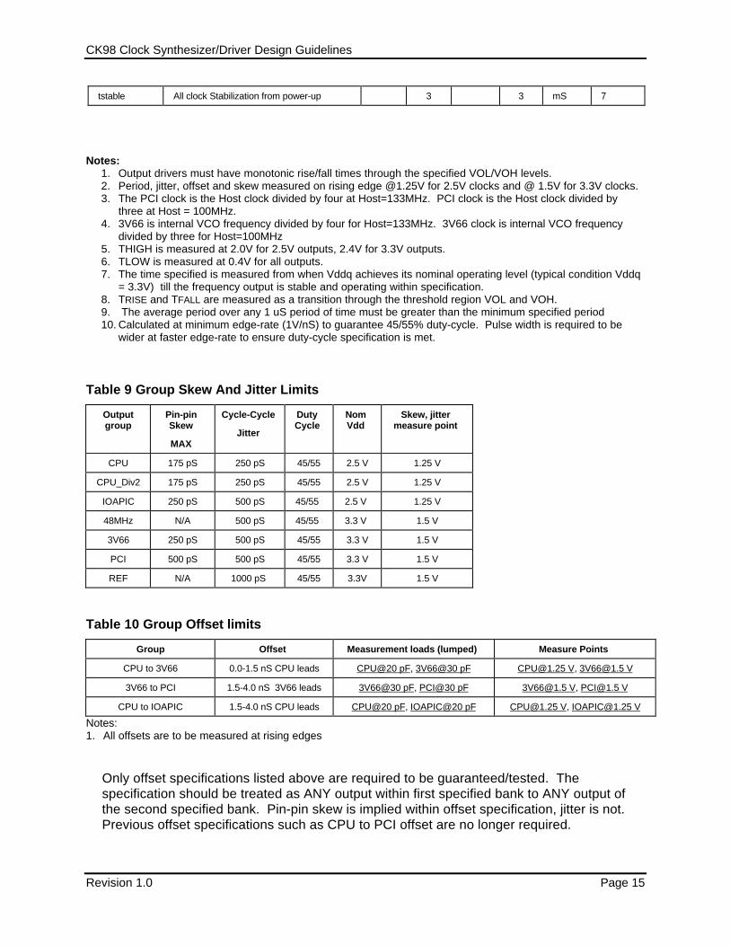
Table 9 Group Skew And Jitter Limits
Outputgroup
Pin-pinSkew
MAX
Cycle-Cycle
Jitter
DutyCycle
NomVdd
Skew, jittermeasure point
CPU 175 pS 250 pS 45/55 2.5 V 1.25 V
CPU_Div2 175 pS 250 pS 45/55 2.5 V 1.25 V
IOAPIC 250 pS 500 pS 45/55 2.5 V 1.25 V
48MHz N/A 500 pS 45/55 3.3 V 1.5 V
3V66 250 pS 500 pS 45/55 3.3 V 1.5 V
PCI 500 pS 500 pS 45/55 3.3 V 1.5 V
REF N/A 1000 pS 45/55 3.3V 1.5 V
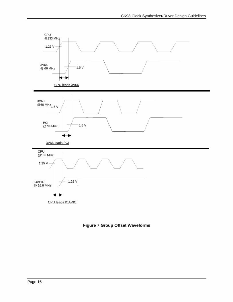
Table 10 Group Offset limits
Group Offset Measurement loads (lumped) Measure Points
CPU to 3V66 0.0-1.5 nS CPU leads CPU@20 pF, 3V66@30 pF [email protected] V, [email protected] V
3V66 to PCI 1.5-4.0 nS 3V66 leads 3V66@30 pF, PCI@30 pF [email protected] V, [email protected] V
CPU to IOAPIC 1.5-4.0 nS CPU leads CPU@20 pF, IOAPIC@20 pF [email protected] V, [email protected] V
Notes:1. All offsets are to be measured at rising edges
Only offset specifications listed above are required to be guaranteed/tested. Thespecification should be treated as ANY output within first specified bank to ANY output ofthe second specified bank. Pin-pin skew is implied within offset specification, jitter is not.Previous offset specifications such as CPU to PCI offset are no longer required.
CK98 Clock Synthesizer/Driver Design Guidelines
Page 16
CPU@133 MHz
3V66@ 66 MHz
CPU leads 3V66
1.5 V
1.25 V
3V66@66 MHz
PCI@ 33 MHz
3V66 leads PCI
1.5 V
1.5 V
CPU@133 MHz
IOAPIC@ 16.6 MHz
CPU leads IOAPIC
1.25 V
1.25 V
Figure 7 Group Offset Waveforms
CK98 Clock Synthesizer/Driver Design Guidelines
Revision 1.0 Page 17
3.1.1 Frequency Accuracy of 48MHz outputsThe 48 MHz PPM of the nominal frequency is REQUIRED to be +167 from 48.00MHz toconform to the USB default frequency accuracy specification.
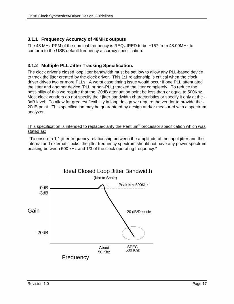
3.1.2 Multiple PLL Jitter Tracking Specification.The clock driver’s closed loop jitter bandwidth must be set low to allow any PLL-based deviceto track the jitter created by the clock driver. This 1:1 relationship is critical when the clockdriver drives two or more PLLs. A worst case timing issue would occur if one PLL attenuatedthe jitter and another device (PLL or non-PLL) tracked the jitter completely. To reduce thepossibility of this we require that the -20dB attenuation point be less than or equal to 500Khz.Most clock vendors do not specify their jitter bandwidth characteristics or specify it only at the -3dB level. To allow for greatest flexibility in loop design we require the vendor to provide the -20dB point. This specification may be guaranteed by design and/or measured with a spectrumanalyzer.
This specification is intended to replace/clarify the Pentium® processor specification which wasstated as:
“To ensure a 1:1 jitter frequency relationship between the amplitude of the input jitter and theinternal and external clocks, the jitter frequency spectrum should not have any power spectrumpeaking between 500 kHz and 1/3 of the clock operating frequency.”
Gain
Frequency
-3dB
-20dB
500 Khz About50 Khz
0dB
Ideal Closed Loop Jitter Bandwidth
-20 dB/Decade
SPEC
(Not to Scale)
Peak is < 500Khz
CK98 Clock Synthesizer/Driver Design Guidelines
Page 18
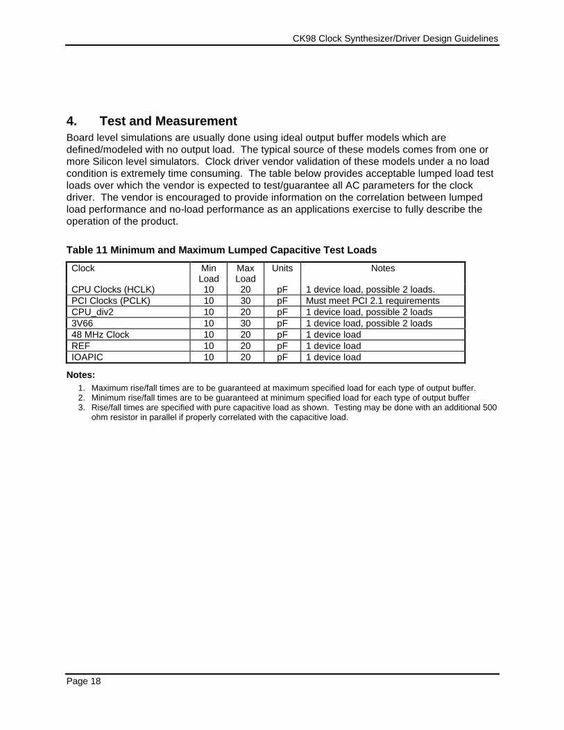
4. Test and MeasurementBoard level simulations are usually done using ideal output buffer models which aredefined/modeled with no output load. The typical source of these models comes from one ormore Silicon level simulators. Clock driver vendor validation of these models under a no loadcondition is extremely time consuming. The table below provides acceptable lumped load testloads over which the vendor is expected to test/guarantee all AC parameters for the clockdriver. The vendor is encouraged to provide information on the correlation between lumpedload performance and no-load performance as an applications exercise to fully describe theoperation of the product.
Table 11 Minimum and Maximum Lumped Capacitive Test Loads
Clock MinLoad
MaxLoad
Units Notes
CPU Clocks (HCLK) 10 20 pF 1 device load, possible 2 loads.PCI Clocks (PCLK) 10 30 pF Must meet PCI 2.1 requirementsCPU_div2 10 20 pF 1 device load, possible 2 loads3V66 10 30 pF 1 device load, possible 2 loads48 MHz Clock 10 20 pF 1 device loadREF 10 20 pF 1 device loadIOAPIC 10 20 pF 1 device load
Notes:1. Maximum rise/fall times are to be guaranteed at maximum specified load for each type of output buffer.2. Minimum rise/fall times are to be guaranteed at minimum specified load for each type of output buffer3. Rise/fall times are specified with pure capacitive load as shown. Testing may be done with an additional 500
ohm resistor in parallel if properly correlated with the capacitive load.
CK98 Clock Synthesizer/Driver Design Guidelines
Revision 1.0 Page 19
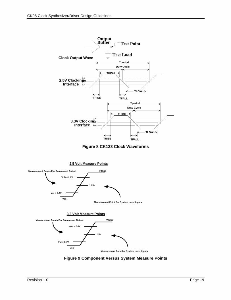
Clock Output WaveForm
TRISE
2.0
0.4
Tperiod
1.25
THIGH
TLOW
Duty Cycle
2.5V ClockingInterface
OutputBuffer Test Point
Test Load
TFALL
TRISE
2.4
0.4
Tperiod
1.5
THIGH
TLOW
Duty Cycle
3.3V ClockingInterface
TFALL
Figure 8 CK133 Clock Waveforms
Vol = 0.4V
1.25V
Voh = 2.0V
Measurement Points For Component Output
Measurement Point For System Level Inputs
Vddq2
Vss
Vol = 0.4V
1.5V
Voh = 2.4V
Measurement Points For Component Output
Measurement Point for System Level Inputs
Vddq3
Vss
2.5 Volt Measure Points
3.3 Volt Measure Points
Figure 9 Component Versus System Measure Points
CK98 Clock Synthesizer/Driver Design Guidelines
Page 20
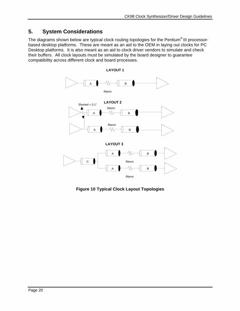
5. System ConsiderationsThe diagrams shown below are typical clock routing topologies for the Pentium® III processor-based desktop platforms. These are meant as an aid to the OEM in laying out clocks for PCDesktop platforms. It is also meant as an aid to clock driver vendors to simulate and checktheir buffers. All clock layouts must be simulated by the board designer to guaranteecompatibility across different clock and board processes.
LAYOUT 1
A
Rterm
B
LAYOUT 2
A
Rterm
B
A
Rterm
B
A
Rterm
B
C
LAYOUT 3
A
Rterm
B
Shorted < 0.1"
Figure 10 Typical Clock Layout Topologies
CK98 Clock Synthesizer/Driver Design Guidelines
Revision 1.0 Page 21
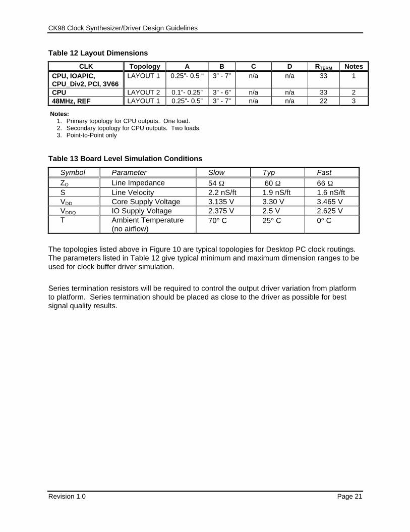
Table 12 Layout Dimensions
CLK Topology A B C D RTERM NotesCPU, IOAPIC,CPU_Div2, PCI, 3V66
LAYOUT 1 0.25”- 0.5 “ 3” - 7” n/a n/a 33 1
CPU LAYOUT 2 0.1”- 0.25” 3” - 6” n/a n/a 33 248MHz, REF LAYOUT 1 0.25”- 0.5” 3” - 7” n/a n/a 22 3
Notes:1. Primary topology for CPU outputs. One load.2. Secondary topology for CPU outputs. Two loads.3. Point-to-Point only
Table 13 Board Level Simulation Conditions
Symbol Parameter Slow Typ FastZO Line Impedance 54 Ω 60 Ω 66 ΩS Line Velocity 2.2 nS/ft 1.9 nS/ft 1.6 nS/ftVDD Core Supply Voltage 3.135 V 3.30 V 3.465 VVDDQ IO Supply Voltage 2.375 V 2.5 V 2.625 VT Ambient Temperature
(no airflow)70° C 25° C 0° C
The topologies listed above in Figure 10 are typical topologies for Desktop PC clock routings.The parameters listed in Table 12 give typical minimum and maximum dimension ranges to beused for clock buffer driver simulation.
Series termination resistors will be required to control the output driver variation from platformto platform. Series termination should be placed as close to the driver as possible for bestsignal quality results.
CK98 Clock Synthesizer/Driver Design Guidelines
Page 22
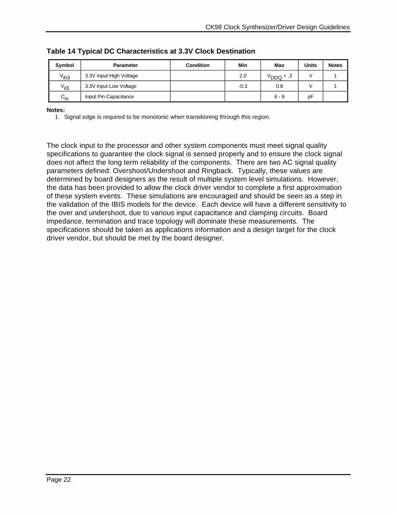
Table 14 Typical DC Characteristics at 3.3V Clock Destination
Symbol Parameter Condition Min Max Units Notes
Vih3 3.3V Input High Voltage 2.0 VDDQ + .3 V 1
Vil3 3.3V Input Low Voltage -0.3 0.8 V 1
Cin Input Pin Capacitance 6 - 9 pF
Notes:1. Signal edge is required to be monotonic when transitioning through this region.
The clock input to the processor and other system components must meet signal qualityspecifications to guarantee the clock signal is sensed properly and to ensure the clock signaldoes not affect the long term reliability of the components. There are two AC signal qualityparameters defined: Overshoot/Undershoot and Ringback. Typically, these values aredetermined by board designers as the result of multiple system level simulations. However,the data has been provided to allow the clock driver vendor to complete a first approximationof these system events. These simulations are encouraged and should be seen as a step inthe validation of the IBIS models for the device. Each device will have a different sensitivity tothe over and undershoot, due to various input capacitance and clamping circuits. Boardimpedance, termination and trace topology will dominate these measurements. Thespecifications should be taken as applications information and a design target for the clockdriver vendor, but should be met by the board designer.
CK98 Clock Synthesizer/Driver Design Guidelines
Revision 1.0 Page 23
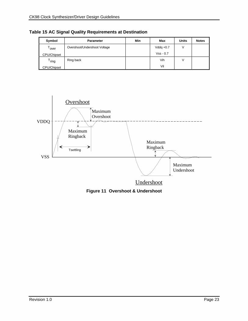
Table 15 AC Signal Quality Requirements at Destination
Symbol Parameter Min Max Units Notes
Tover
CPU/Chipset
Overshoot/Undershoot Voltage Vddq +0.7
Vss - 0.7
V
Tring
CPU/Chipset
Ring back Vih
Vil
V
VDDQ
MaximumOvershoot
MaximumRingback
MaximumUndershoot
MaximumRingback
Overshoot
Undershoot
VSS
Tsettling
Figure 11 Overshoot & Undershoot
CK98 Clock Synthesizer/Driver Design Guidelines
Page 24
6. How To Obtain Reference Material
6.1 PCI ReferenceThe PCI Special Interest Group is an industry-wide group that controls the official PCIspecification. You can obtain the latest copies of the PCI specification by contacting the PCISpecial Interest Group at the following numbers:
(800) 433-5177 - USA(503) 797-4297 - International(503) 234-6762 - Fax
There is a nominal fee for obtaining this specification.
6.2 IBIS ReferenceThe IBIS Open Forum is an industry-wide forum that controls the official IBIS specification.Minutes of IBIS meetings, email correspondence, proposals for specification changes, etc. areon-line at "vhdl.org". To join in the email discussions, send a message to "[email protected]" and request that your name be added to the IBIS mail reflector. Be sure toinclude your email address.
The IBIS home page can be found at http://www.eia.org/eig/ibis/ibis.htm
6.3 Audio Codec 98 (AC98) ReferenceThe AC97 home page can be found at http://www.intel.com/pc-supp/platform/aud98
6.3 AGP ReferenceAGP information can be found at http://developer.intel.com/solutions/tech/agp.htm
CK98 Clock Synthesizer/Driver Design Guidelines
Revision 1.0 Page 25
7. Appendices
7.1 Appendix A: CK133 56 pin SSOP Pin-out
The following addendum defines a generic pin-out and base requirements for IntelArchitecture based platforms. It is intended to be used with another clock driver toclock the memory devices. This appendix can be used as an example for developmentof other custom clock components. This is not the only solution that can be derived.
Features (56 Pin SSOP Package):• Four copies of CPU Clock• Eight copies of PCI Clock (Synchronous w/CPU Clock). One free running PCI.• Two CPU/2 outputs for synchronous memory reference• Four copies of fixed frequency 3.3V Clock• Three copies of IOAPIC Clock @16.667 MHz, synchronous to CPU Clock• One copy of 48MHz Clock• Two copies of Ref. Clock @14.31818 MHz• Ref. 14.31818MHz Xtal Oscillator Input• 133MHz or 100MHz operation• Power Management Control Input Pins
VssREF0REF1
Vdd3VXTAL_IN
XTAL_OUTVss
PCICLK_FPCICLK1
Vdd3VPCICLK2PCICLK3
VssPCICLK4PCICLK5
Vdd3VPCICLK6PCICLK7
VssVss
3V66_03V66_1Vdd3V
Vss3V66_23V66_3Vdd3V
SEL133/100#
Vdd25VAPIC2APIC1APIC0VssVdd25VCPU_div2CPU_div2VssVdd25VCPUCLK3CPUCLK2VssVdd25VCPUCLK1CPUCLK0VssVdd3VVssPCISTOP#CPUSTOP#PWRDWN#SPREAD#SEL1SEL0Vdd3V48MhzVss
12345678910111213141516171819202122232425262728
56555453525150494847464544434241403938373635343332313029
CK133
2.5V Supply
CK98 Clock Synthesizer/Driver Design Guidelines
Page 26
Table 16 CK133 Pin Description Table
Pin Type Qty Symbol Description
2,3 output 2 REF [0-1] 3.3V 14.318 MHz clock output
5 input 1 XTAL_IN 14.318 MHz Crystal input
6 output 1 XTAL_OUT 14.318 MHz Crystal output
8 output 1 PCICLK_F 3.3V Free running PCI clock
9,11,12,14,15,17,18 output 7 PCICLK [1-7] 3.3V PCI clock outputs
21,22,25,26 output 4 3V66 [0-3] 3.3V Fixed 66MHz clock outputs
28 input 1 SEL133/100# 3.3V LVTTL compatible input for 133MHz or 100MHz CPUoutputs.
H = 133MHz, L = 100MHz
30 output 1 48MHz 3.3V Fixed 48MHz clock output
32,33 input 2 SEL [0-1] 3.3V LVTTL compatible inputs for logic selection
34 input 1 SPREAD# 3.3V LVTTL compatible input. Enables spread spectrummode when held LOW
35 input 1 PWRDWN# 3.3V LVTTL compatible input. Device enters power-downmode when held LOW
36 input 1 CPUSTOP# 3.3V LVTTL compatible input. Stops all CPU, and 3V66clocks when held LOW. CPU_div2 output remains on allthe time.
37 input 1 PCISTOP# 3.3V LVTTL compatible input. Stops all PCI clocks exceptPCICLK_F when held LOW
41,42,45,46 output 4 CPUCLK [0-3] 2.5V Host bus clock output. 133MHz or 100MHzdepending on state of SEL133/100#
49,50 output 2 CPU_div2[0-1] 2.5V output running at 1/2 CPU (Host bus) clockfrequency. 66MHz or 50MHz depending on stateSEL133/100#
53,54,55 output 3 APIC [0-2] 2.5V clock outputs running divide synchronous with theCPU (Host bus) clock frequency. Fixed 16.67MHz limit.
If CPU = 133MHz, APIC = CPU/8
If CPU = 100MHz, APIC = CPU/6
4,10,16,23,27,31,39 3.3V Power 7 Vdd3V 3.3V power supply
1,7,13,19,20,24,29,38,40,44,48,52
Vss 12 Vss Ground
43,47,51,56 2.5V Power 4 Vdd25V 2.5V power
CK98 Clock Synthesizer/Driver Design Guidelines
Revision 1.0 Page 27
7.1.1 Spread Spectrum Clocking (SSC) Clarification:Spread Spectrum functionality on the CK133 clock driver is required by most OEMs and actsas an on/off switch for different forms of spread spectrum modulation techniques. Any givenOEM may or may not use this feature due to platform-level timing issues. The followingspecifications are added to the current CK133 definition:
1. No external modulation frequency source is required by the CK133.2. Vendor needs to synchronously modulate all the CPU, PCI, APIC, 3V66, and CPU/2
output clocks. REF and fixed frequency 48MHz clock outputs are not modulated.3. All device timings (including jitter, skew, min-max clock period, output rise/fall time)
MUST meet the existing non-spread spectrum specifications4. All non-spread CPU and PCI functionality must be maintained in the spread
spectrum mode (includes all power management functions.)5. The minimum clock period cannot be violated. The preferred method is to adjust
the spread technique to not allow for modulation above the nominal frequency.This technique is often called “down-spreading”. An example triangular frequencymodulation profile is shown in Figure 12. The modulation profile in a modulationperiod can be expressed as:
<<⋅⋅⋅−+
<<⋅⋅⋅+−=
, )(
; )(
mmnommnom
mnommnom
f1
tf21
when tff2f1
f21
t0when tff2f1f
δδ
δδ
where fnom is the nominal frequency in the non-SSC mode, fm is the modulationfrequency, δ is the modulation amount, and t is time.
(1-δ)fnom
fnom
1/fmt
0.5/fm
Figure 12 Triangular Frequency Modulation Profile.
6. For triangular modulation, the clock frequency deviation (δ) is required to be no
more than 0.6% “down-spread” from the corresponding nominal frequency, i.e.,+0%/-0.6%. The absolute spread amount at the fundamental frequency is shown inFigure 13, as the width of its spectral distribution (between the -3dB roll-off). Theratio of this width to the fundamental frequency cannot exceed 0.6%. Thisparameter can be measured in the frequency domain using a spectrum analyzer.The amount of allowed spreading for any non-triangular modulation is determinedby the induced downstream PLL tracking skew (see explanation in 8), which cannotexceed that of a 0.6% triangular modulation. Typically, it is about 0.5%.
CK98 Clock Synthesizer/Driver Design Guidelines
Page 28
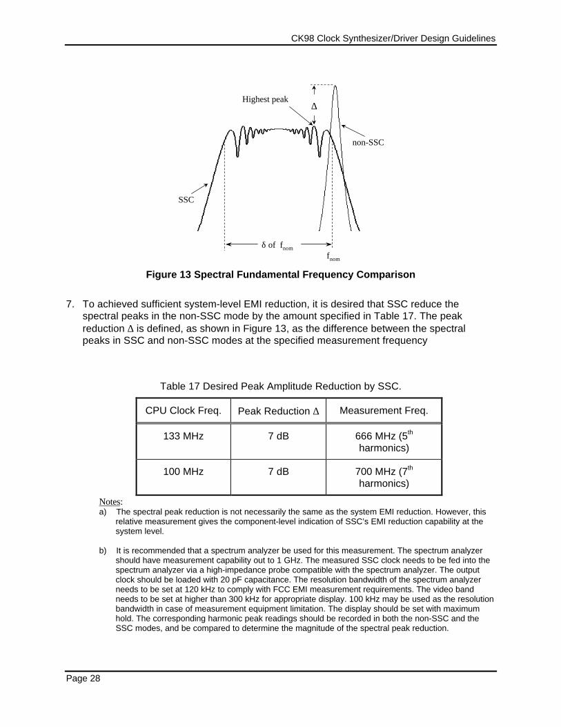
∆
SSC
non-SSC
Highest peak
δ of fnom
fnom
Figure 13 Spectral Fundamental Frequency Comparison
7. To achieved sufficient system-level EMI reduction, it is desired that SSC reduce the
spectral peaks in the non-SSC mode by the amount specified in Table 17. The peakreduction ∆ is defined, as shown in Figure 13, as the difference between the spectralpeaks in SSC and non-SSC modes at the specified measurement frequency
Table 17 Desired Peak Amplitude Reduction by SSC.
CPU Clock Freq. Peak Reduction ∆ Measurement Freq.
133 MHz 7 dB 666 MHz (5th
harmonics)
100 MHz 7 dB 700 MHz (7th
harmonics)
Notes:a) The spectral peak reduction is not necessarily the same as the system EMI reduction. However, this
relative measurement gives the component-level indication of SSC’s EMI reduction capability at thesystem level.
b) It is recommended that a spectrum analyzer be used for this measurement. The spectrum analyzershould have measurement capability out to 1 GHz. The measured SSC clock needs to be fed into thespectrum analyzer via a high-impedance probe compatible with the spectrum analyzer. The outputclock should be loaded with 20 pF capacitance. The resolution bandwidth of the spectrum analyzerneeds to be set at 120 kHz to comply with FCC EMI measurement requirements. The video bandneeds to be set at higher than 300 kHz for appropriate display. 100 kHz may be used as the resolutionbandwidth in case of measurement equipment limitation. The display should be set with maximumhold. The corresponding harmonic peak readings should be recorded in both the non-SSC and theSSC modes, and be compared to determine the magnitude of the spectral peak reduction.
CK98 Clock Synthesizer/Driver Design Guidelines
Revision 1.0 Page 29
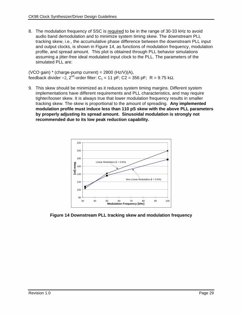
8. The modulation frequency of SSC is required to be in the range of 30-33 kHz to avoidaudio band demodulation and to minimize system timing skew. The downstream PLLtracking skew, i.e., the accumulative phase difference between the downstream PLL inputand output clocks, is shown in Figure 14, as functions of modulation frequency, modulationprofile, and spread amount. This plot is obtained through PLL behavior simulationsassuming a jitter-free ideal modulated input clock to the PLL. The parameters of thesimulated PLL are:
(VCO gain) * (charge-pump current) = 2800 (Hz/V)(A), feedback divider =2, 2nd-order filter: C1 = 11 pF; C2 = 356 pF; R = 9.75 kΩ. 9. This skew should be minimized as it reduces system timing margins. Different system
implementations have different requirements and PLL characteristics, and may requiretighter/looser skew. It is always true that lower modulation frequency results in smallertracking skew. The skew is proportional to the amount of spreading. Any implementedmodulation profile must induce less than 110 pS skew with the above PLL parametersby properly adjusting its spread amount. Sinusoidal modulation is strongly notrecommended due to its low peak reduction capability.
80
100
120
140
160
180
200
220
30 40 50 60 70 80 90 100Modulation Frequency [kHz]
Skew
[ps]
Linear Modulation (δ = 0.6%)
Non-Linear Modulation (δ = 0.5%)
Figure 14 Downstream PLL tracking skew and modulation frequency
CK98 Clock Synthesizer/Driver Design Guidelines
Page 30
7.1.2 IOAPIC Clock Outputs Required To Be Synchronous With CPUCLKThe IOAPIC clocks, which were previously obtained by buffering the input reference crystalfrequency, are now required to be synchronous with the CPUCLK outputs. The IOAPICvoltage will track that of the Host bus and will have a maximum frequency of 16.667MHz. TheIOAPIC clocks will be derived by dividing the CPUCLK outputs by eight when the Host bus is133.33MHz, and by six when the Host bus is 100MHz. The IOAPIC clocks will lag the Hostbus clocks by 1.5-4.0 nS at the maximum device load (20pF.)
This functionality is to be defined to allow the clock driver to meet the previously optional“functional redundancy check (FRC) mode.” However, it is believed that the synchronousIOAPIC clocks will help reduce the jitter variation seen across vendors by allowing a commondecoupling scheme for IOAPIC noise.
Table 18 CK133 Select Functions
SEL133/100# SEL1 SEL0 Function
0 0 0 All outputs Tri-State0 0 1 (Reserved)0 1 0 Active 100MHz, 48MHz PLL
inactive0 1 1 Active 100MHz, 48MHz PLL active1 0 0 Test Mode1 0 1 (Reserved)1 1 0 Active 133MHz, 48MHz PLL
inactive1 1 1 Active 133MHz, 48MHz PLL active
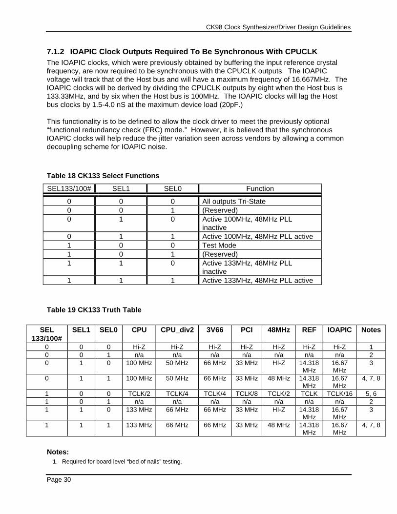
Table 19 CK133 Truth Table
SEL133/100#
SEL1 SEL0 CPU CPU_div2 3V66 PCI 48MHz REF IOAPIC Notes
0 0 0 Hi-Z Hi-Z Hi-Z Hi-Z Hi-Z Hi-Z Hi-Z 10 0 1 n/a n/a n/a n/a n/a n/a n/a 20 1 0 100 MHz 50 MHz 66 MHz 33 MHz HI-Z 14.318
MHz16.67MHz
3
0 1 1 100 MHz 50 MHz 66 MHz 33 MHz 48 MHz 14.318MHz
16.67MHz
4, 7, 8
1 0 0 TCLK/2 TCLK/4 TCLK/4 TCLK/8 TCLK/2 TCLK TCLK/16 5, 61 0 1 n/a n/a n/a n/a n/a n/a n/a 21 1 0 133 MHz 66 MHz 66 MHz 33 MHz HI-Z 14.318
MHz16.67MHz
3
1 1 1 133 MHz 66 MHz 66 MHz 33 MHz 48 MHz 14.318MHz
16.67MHz
4, 7, 8
Notes:1. Required for board level “bed of nails” testing.
CK98 Clock Synthesizer/Driver Design Guidelines
Revision 1.0 Page 31
2. Used to support Intel confidential application. Contact Intel representative for more details.3. 48MHz PLL disabled to reduce component jitter. Vendor expected to tighten jitter spec in this mode to
<200pS. 48 MHz outputs to be held HI-Z instead of driven to a LOW state.4. “Normal” mode of operation5. TCLK is a test clock over driven on the XTAL_IN input during test mode. TCLK mode is based on 133 MHz
CPU select logic.6. Required for DC output impedance verification7. Range of reference frequency allowed is min = 14.316 nominal = 14.31818 MHz, max = 14.32 MHz.8. Frequency accuracy of 48MHz must be +167PPM to match USB default. See Section 3.1.1 for details
7.1.2 Non-production Processor Frequencies For System DebugSome system debug applications exist where processor frequencies that are above and belowthe specified 100, 133 MHz are of interest for this device. The ability to use this device in a labenvironment using a 10 or 20 MHz crystal is desired. Another desired feature of this product isthe ability to use a function generator (in lab environment only) to drive XTAL_IN (floatXTAL_OUT) in test mode to create up to a 66 MHz CPU output.
7.1.3 CK133 System Considerations:The SEL133/100# frequency select pin requires a specific motherboard pull-up resistor(preliminary = 220 Ohms) to 3.3V to allow the CK133 device to sense the maximum Host busfrequency of the processor to automatically configure the CK133 to either 133 or 100MHz.
No internal pull-up or pull-down resistors are allowed on the SEL100/133# pin.
7.1.4 CK133 Power ManagementThe following power-consumption conditions for the device should be tested/guaranteed byeach vendor. The values below are estimates for the power specs.
Table 20 CK133 Maximum Allowed Current
CK133Condition
Max 2.5V supply consumptionMax discrete cap loads,
Vddq2 = 2.625VAll static inputs = Vddq3 or Vss
Max 3.3V supply consumptionMax discrete cap loads
Vddq3 = 3.465VAll static inputs = Vddq3 or Vss.
Power-down Mode(PWRDWN# = 0)
100 uA 200 uA
Full Active 100 MHzSEL133/100# = 0
SEL1, 0 = 11CPUSTOP#, PCISTOP# = 1
75 mA 160 mA
Full Active 133 MHzSEL133/100# = 1
SEL1,0 = 11
90 mA 160 mA
CK98 Clock Synthesizer/Driver Design Guidelines
Page 32
CPUSTOP#, PCISTOP# = 1
The power-down controller provides a signal that is latched with its own copy of the PCI clock.In theory, this should be synchronous with the clock driver output IF the following is quantified:
1. The flight time of the clock trace from PCI clock to the controller2. Input edge-rate at the controller, input load at the controller, set/hold time at the controller.3. Variance of output edge-rate from PCI of clock driver4. Internal delay from output of PCI on clock driver to internal clock signal
However, the large number of platform level variables that must be taken into account for theinput to be described as “synchronous” to the clock driver output is large and highly dependenton the board design. To simplify the platform design, the CPU_STOP# and the PCI_STOP#inputs are defined to be ASYNCHRONOUS from the clock driver external PCI clock. The clockdriver must synchronize the input signal and resynchronize it with its own PCI clock output.This leaves the board timing issues up to the board designer rather than the clock vendor.
Clock sequencing must always guarantee full clock timing parameters at all times after thesystem has initially powered up except where noted. During power up and power downoperations using the PWR_DWN# select pin, partial clocks are not allowed and all clock timingparameters must be met except for the following. It is understood that the first clock pulsecoming out of a stopped clock condition could be slightly distorted due to clock networkcharging requirements. It is also understood that board routing and signal loading have a largeimpact on the initial clock distortion.
7.1.5 Vdd3v Power-down Removal: RequiredThere is a specific power-down procedure that will be used by some platform implementationsof this device. The CK133 device is required to meet the following requirement to allow for acommon design across multiple platforms.
To allow for multiple devices in platforms to share voltage regulators, the CK133 must be ableto allow the removal of power from the Vdd3v voltage pins during the following specificcondition. Leakage currents from the Vdd3v and Vdd25v pins are not allowed to violateexisting powerdown# specifications.
Going into power-down mode:1) Assert the PWRDWN# signal to the CK133.2) Remove power from the 3.3V pins of the CK133.3) All input pins of CK133 will be either powered down or driven to ground.4) The Vdd3 power plane will be pulled to or discharge to <250 mV.5) The 2.5V pins will remain powered at 2.5V.
Restore power:1) Apply 3.3V to the CK133.2) Wait 200 - 2000mSec3) De-assert the PWRDWN# signal4) Wait longer than lock time specified for device
CK98 Clock Synthesizer/Driver Design Guidelines
Revision 1.0 Page 33
5) Continue operation as normal
CK98 Clock Synthesizer/Driver Design Guidelines
Page 34
Table 21 CK133 Clock Enable Configuration
CPU_STOP# PWR_DWN# PCI_STOP# CPUCLK CPU_div2 APIC 3V66 PCI PCI_F REF,48Mhz
Osc VCOs
X 0 X LOW LOW LOW LOW LOW LOW LOW OFF OFF
0 1 0 LOW ON ON LOW LOW ON ON ON ON
0 1 1 LOW ON ON LOW ON ON ON ON ON
1 1 0 ON ON ON ON LOW ON ON ON ON
1 1 1 ON ON ON ON ON ON ON ON ON
Notes:1. LOW means outputs held static LOW as per latency requirement below.2. ON means active.3. PWR_DWN# pulled LOW, impacts all outputs including REF and 48 MHz outputs.4. All 3V66 as well as all CPU clocks should stop cleanly when CPU_STOP# is pulled LOW.5. CPU_div2, IOAPIC, REF, 48MHz signals are not controlled by the CPU_STOP# functionality and are enabled
all in all conditions except PWR_DWN#=LOW.
Table 22 CK133 Power Management Requirements
Latency
Signal Signal State No. of rising edges of PCICLK
CPU_STOP# 0 (disabled) 1
1 (enabled) 1
PCI_STOP# 0 (disabled) 1
1 (enabled) 1
PWR_DWN# 1 (normal operation) 3 mS
0 (power down) 2 max.
Notes:1. Clock on/off latency is defined in the number of rising edges of free running PCICLKs between the clock disable goes low/high to
the first valid clock comes out of the device.2. Power up latency is when PWR_DWN# goes inactive (high) to when the first valid clocks are driven from the device.
CK98 Clock Synthesizer/Driver Design Guidelines
Revision 1.0 Page 35
CPU_STOP# is an input to the clock synthesizer. It is used to turn off the CPU and 3V66clocks for low power operation. CPU_STOP# is asserted asynchronously by the external clockcontrol logic with the rising edge of free running PCI clock (and hence CPU clock) and must beinternally synchronized to the external PCI_F output. All other clocks will continue to run whilethe CPU clocks are disabled. The CPU clocks must always be stopped in a low state andstarted in such a manner as to guarantee that the high pulse width is a full pulse. ONLY onerising edge of PCI_F is allowed after the clock control logic switched for both the CPU and3V66 outputs to become enabled/disabled.
CPUCLK(internal)
PCICLK(internal)
CPU_STOP#
PCI_STOP#
PWR_DWN#
CPUCLK(external)
PCI_F(External)
3V66(external)
Figure 15 CK33 CPU_STOP# Timing Diagram
Notes:1. All internal timing is referenced to the CPUCLK2. The Internal label means inside the chip and is a reference only. This in fact may not be the way that the control is designed.3. CPU_STOP# signal is an input signal that must be made synchronous to free running PCI_F4. 3V66 clocks also stop/start before one rising edge of PCI_F when CPU_STOP# is asserted/deasserted.5. PWR_DWN# and PCI_STOP# are shown in a high state.6. Diagrams shown with respect to 133MHz. Similar operation when CPU is 100MHz
CK98 Clock Synthesizer/Driver Design Guidelines
Page 36
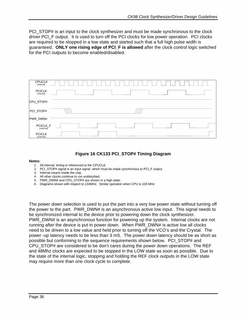
PCI_STOP# is an input to the clock synthesizer and must be made synchronous to the clockdriver PCI_F output. It is used to turn off the PCI clocks for low power operation. PCI clocksare required to be stopped in a low state and started such that a full high pulse width isguaranteed. ONLY one rising edge of PCI_F is allowed after the clock control logic switchedfor the PCI outputs to become enabled/disabled.
CPUCLK(internal)
PCICLK(internal)
CPU_STOP#
PCI_STOP#
PWR_DWN#
PCICLK(external)
PCICLK_F(external)
Figure 16 CK133 PCI_STOP# Timing Diagram
Notes:1. All internal timing is referenced to the CPUCLK.2. PCI_STOP# signal is an input signal which must be made synchronous to PCI_F output.3. Internal means inside the chip.4. All other clocks continue to run undisturbed.5. PWR_DWN# and CPU_STOP# are shown in a high state.6. Diagrams shown with respect to 133MHz. Similar operation when CPU is 100 MHz
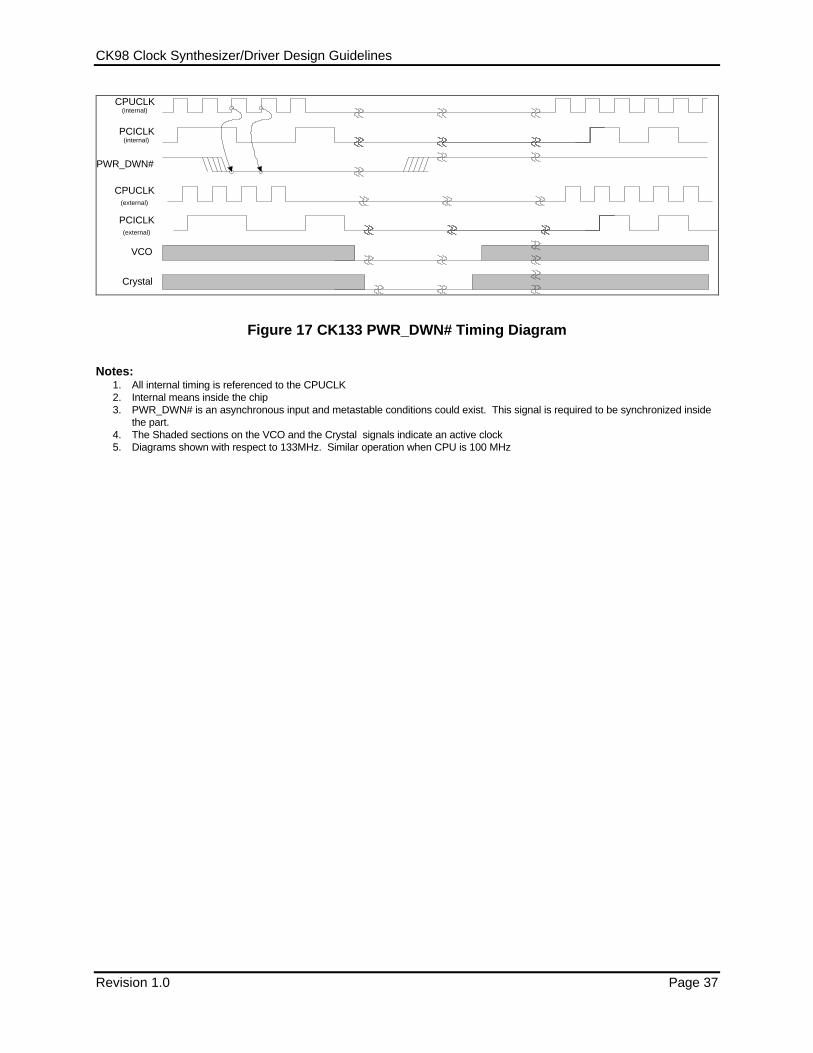
The power down selection is used to put the part into a very low power state without turning offthe power to the part. PWR_DWN# is an asynchronous active low input. This signal needs tobe synchronized internal to the device prior to powering down the clock synthesizer.PWR_DWN# is an asynchronous function for powering up the system. Internal clocks are notrunning after the device is put in power down. When PWR_DWN# is active low all clocksneed to be driven to a low value and held prior to turning off the VCO’s and the Crystal. Thepower -up latency needs to be less than 3 mS. The power down latency should be as short aspossible but conforming to the sequence requirements shown below. PCI_STOP# andCPU_STOP# are considered to be don’t cares during the power down operations. The REFand 48Mhz clocks are expected to be stopped in the LOW state as soon as possible. Due tothe state of the internal logic, stopping and holding the REF clock outputs in the LOW statemay require more than one clock cycle to complete.
CK98 Clock Synthesizer/Driver Design Guidelines
Revision 1.0 Page 37
CPUCLK(internal)
PCICLK(internal)
PWR_DWN#
PCICLK(external)
CPUCLK(external)
VCO
Crystal
Figure 17 CK133 PWR_DWN# Timing Diagram
Notes:1. All internal timing is referenced to the CPUCLK2. Internal means inside the chip3. PWR_DWN# is an asynchronous input and metastable conditions could exist. This signal is required to be synchronized inside
the part.4. The Shaded sections on the VCO and the Crystal signals indicate an active clock5. Diagrams shown with respect to 133MHz. Similar operation when CPU is 100 MHz
CK98 Clock Synthesizer/Driver Design Guidelines
Page 38
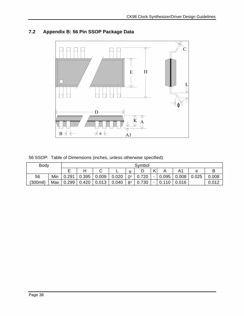
7.2 Appendix B: 56 Pin SSOP Package Data
56 SSOP: Table of Dimensions (inches, unless otherwise specified)
Body SymbolE H C L φ D K A A1 e B
56 Min 0.291 0.395 0.009 0.020 0° 0.720 - 0.095 0.008 0.025 0.008(300mil) Max 0.299 0.420 0.013 0.040 8° 0.730 - 0.110 0.016 0.012
UNITED STATES, Intel Corporation2200 Mission College Blvd., P.O. Box 58119, Santa Clara, CA 95052-8119
Tel: +1 408 765-8080
JAPAN, Intel Japan K.K.5-6 Tokodai, Tsukuba-shi, Ibaraki-ken 300-26
Tel: + 81-29847-8522
FRANCE, Intel Corporation S.A.R.L.1, Quai de Grenelle, 75015 Paris
Tel: +33 1-45717171
UNITED KINGDOM, Intel Corporation (U.K.) Ltd.Pipers Way, Swindon, Wiltshire, England SN3 1RJ
Tel: +44 1-793-641440
GERMANY, Intel GmbHDornacher Strasse 1
85622 Feldkirchen/ MuenchenTel: +49 89/99143-0
HONG KONG, Intel Semiconductor Ltd.32/F Two Pacific Place, 88 Queensway, Central
Tel: +852 2844-4555
CANADA, Intel Semiconductor of Canada, Ltd.190 Attwell Drive, Suite 500Rexdale, Ontario M9W 6H8
Tel: +416 675-2438
BRAZIL, Intel Semicondutores do BrasilCentro Empresarial Nações Unidas - Edifício Torre Oeste
Av. das Nações Unidas, 12.901 - 18o. andar - Brooklin Novo04578.000 São Paulo - S.P. – Brasil
Tel: +55-11-5505-2296