Embed Size (px)
Citation preview

COLOR MONITORSERVICE MANUAL
Website:http://biz.LGservice.comE-mail:http://www.LGEservice.com/techsup.html
CAUTIONBEFORE SERVICING THE UNIT, READ THE SAFETY PRECAUTIONS IN THIS MANUAL.
CHASSIS NO. : LP69G
MODEL: M208WA (M208WA-BZH.A**VLP)*( ) **Same model for Service
- 2 -
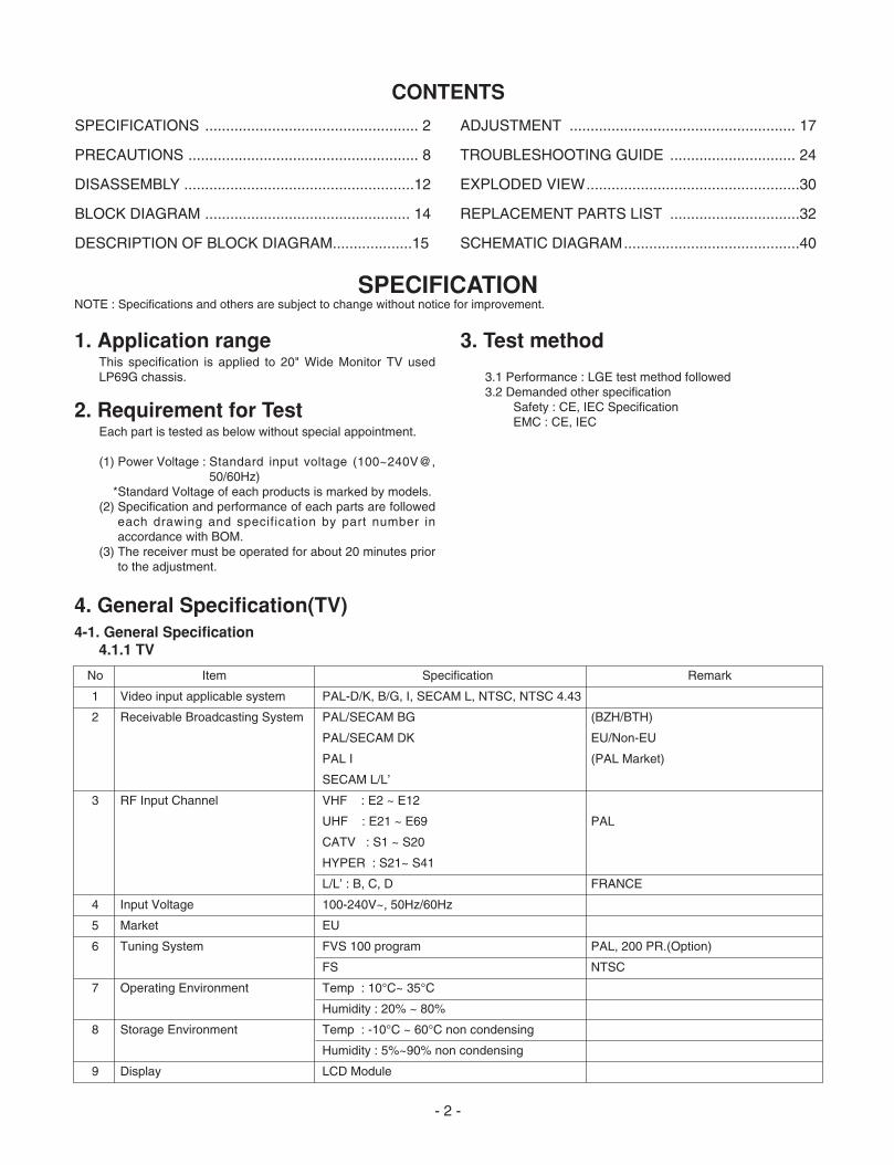
CONTENTS
SPECIFICATIONS ................................................... 2
PRECAUTIONS ....................................................... 8
DISASSEMBLY .......................................................12
BLOCK DIAGRAM ................................................. 14
DESCRIPTION OF BLOCK DIAGRAM...................15
ADJUSTMENT ...................................................... 17
TROUBLESHOOTING GUIDE .............................. 24
EXPLODED VIEW...................................................30
REPLACEMENT PARTS LIST ...............................32
SCHEMATIC DIAGRAM..........................................40
1. Application rangeThis specification is applied to 20" Wide Monitor TV usedLP69G chassis.
2. Requirement for TestEach part is tested as below without special appointment.
(1) Power Voltage : Standard input voltage (100~240V@,50/60Hz)
*Standard Voltage of each products is marked by models.(2) Specification and performance of each parts are followed
each drawing and specification by part number inaccordance with BOM.
(3) The receiver must be operated for about 20 minutes priorto the adjustment.
3. Test method
3.1 Performance : LGE test method followed3.2 Demanded other specification
Safety : CE, IEC SpecificationEMC : CE, IEC
SPECIFICATIONNOTE : Specifications and others are subject to change without notice for improvement.
4-1. General Specification4.1.1 TV
4. General Specification(TV)
No Item Specification Remark
1 Video input applicable system PAL-D/K, B/G, I, SECAM L, NTSC, NTSC 4.43
2 Receivable Broadcasting System PAL/SECAM BG (BZH/BTH)
PAL/SECAM DK EU/Non-EU
PAL I (PAL Market)
SECAM L/L’
3 RF Input Channel VHF : E2 ~ E12
UHF : E21 ~ E69 PAL
CATV : S1 ~ S20
HYPER : S21~ S41
L/L’ : B, C, D FRANCE
4 Input Voltage 100-240V~, 50Hz/60Hz
5 Market EU
6 Tuning System FVS 100 program PAL, 200 PR.(Option)
FS NTSC
7 Operating Environment Temp : 10°C~ 35°C
Humidity : 20% ~ 80%
8 Storage Environment Temp : -10°C ~ 60°C non condensing
Humidity : 5%~90% non condensing
9 Display LCD Module
- 3 -
No. Item Min Typ. Max Unit Remark
1. Type TFT Color LCD Module
2. Active Display area 433.44 (H) x 270.9 (V) mm
3. Outline dimension 459.4 (H) x 296.4 (V) x16.6 (D) mm Typ
4. Pixel pitch 0.258mm (H) x 0.258mm (V) x RGB mm
5. Color arrangement RGB vertical stripe
6. Color Depth 16.7M color
7. Electrical Interface LVDS
8. Surface Treatment Hard coating(3H) & Anti-glare(Haze 25)
9. Operating Mode Normally White
10. Back light Unit 4 CCFL (4 lamps)
11. R/T R.T : 3.6ms + R.T : 1.4ms Typ.
No. Item Specification Remark
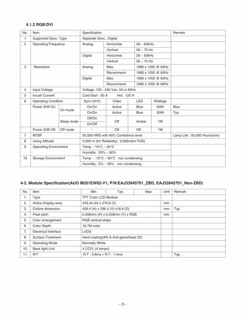
1 Supported Sync. Type Separate Sync., Digital
2 Operating Frequency Analog Horizontal 28 ~ 83kHz
Vertical 56 ~ 75 Hz
Digital Horizontal 28 ~ 83kHz
Vertical 56 ~ 75 Hz
3 Resolution Analog Max. 1680 x 1050 @ 60Hz
Recommend 1680 x 1050 @ 60Hz
Digital Max. 1680 x 1050 @ 60Hz
Recommend 1680 x 1050 @ 60Hz
4 Input Voltage Voltage :100 - 240 Vac, 50 or 60Hz
5 Inrush Current Cold Start : 50 A Hot : 120 A
6 Operating Condition Sync (H/V) Video LED Wattage
Power S/W OnOn mode
On/On Active Blue 60W Max.
On/On Active Blue 50W Typ.
Sleep modeOff/On
Off Amber 1WOn/Off
Power S/W Off Off mode - Off Off 1W
7 MTBF 50,000 HRS with 90% Confidence level Lamp Life : 50,000 Hours(min)
8 Using Altitude 5,000 m (for Reliability) 3,000m(for FOS)
9 Operating Environment Temp : 10°C ~ 35°C
Humidity : 20% ~ 80%
10 Storage Environment Temp : -10°C ~ 60°C non condensing
Humidity : 5% ~ 90% non condensing
4.1.2 RGB/DVI
4-2. Module Specification(AUO M201EW02-V1, P/N:EAJ33945701_ZBD, EAJ33945701_Non-ZBD)
- 4 -
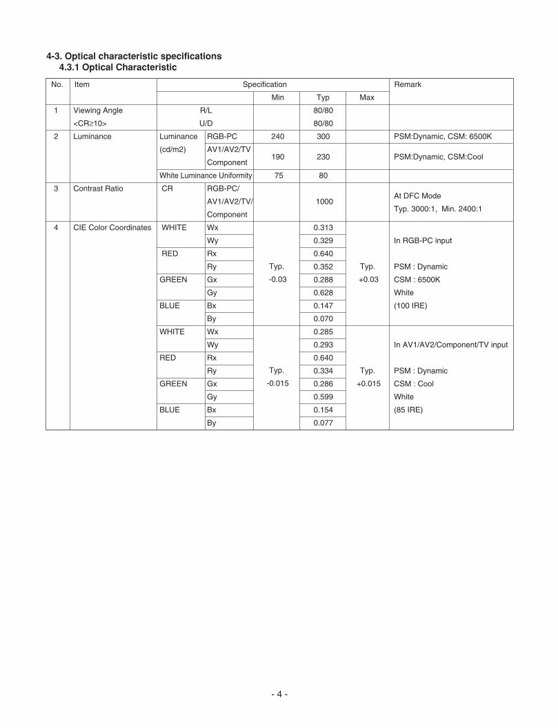
4-3. Optical characteristic specifications4.3.1 Optical Characteristic
No. Item Specification Remark
Min Typ Max
1 Viewing Angle R/L 80/80
<CR≥10> U/D 80/80
2 Luminance Luminance RGB-PC 240 300 PSM:Dynamic, CSM: 6500K
(cd/m2) AV1/AV2/TV190 230 PSM:Dynamic, CSM:Cool
Component
White Luminance Uniformity 75 80
3 Contrast Ratio CR RGB-PC/At DFC Mode
AV1/AV2/TV/ 1000Typ. 3000:1, Min. 2400:1
Component
4 CIE Color Coordinates WHITE Wx 0.313
Wy 0.329 In RGB-PC input
RED Rx 0.640
Ry 0.352 PSM : Dynamic
GREEN Gx 0.288 CSM : 6500K
Gy 0.628 White
BLUE Bx 0.147 (100 IRE)
By 0.070
WHITE Wx 0.285
Wy 0.293 In AV1/AV2/Component/TV input
RED Rx 0.640
Ry 0.334 PSM : Dynamic
GREEN Gx 0.286 CSM : Cool
Gy 0.599 White
BLUE Bx 0.154 (85 IRE)
By 0.077
Typ.
+0.03
Typ.
+0.015
Typ.
-0.03
Typ.
-0.015
- 5 -
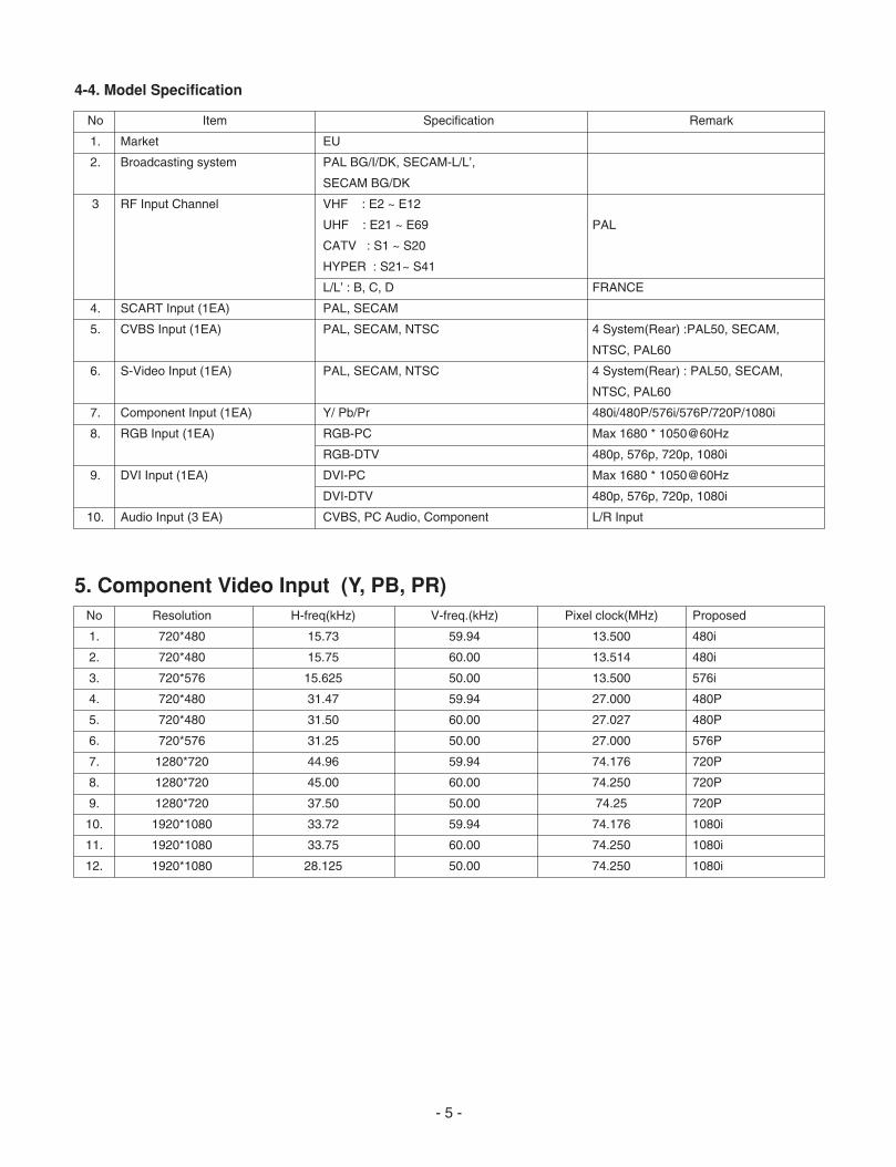
5. Component Video Input (Y, PB, PR)No Resolution H-freq(kHz) V-freq.(kHz) Pixel clock(MHz) Proposed
1. 720*480 15.73 59.94 13.500 480i
2. 720*480 15.75 60.00 13.514 480i
3. 720*576 15.625 50.00 13.500 576i
4. 720*480 31.47 59.94 27.000 480P
5. 720*480 31.50 60.00 27.027 480P
6. 720*576 31.25 50.00 27.000 576P
7. 1280*720 44.96 59.94 74.176 720P
8. 1280*720 45.00 60.00 74.250 720P
9. 1280*720 37.50 50.00 74.25 720P
10. 1920*1080 33.72 59.94 74.176 1080i
11. 1920*1080 33.75 60.00 74.250 1080i
12. 1920*1080 28.125 50.00 74.250 1080i
4-4. Model Specification
No Item Specification Remark
1. Market EU
2. Broadcasting system PAL BG/I/DK, SECAM-L/L’,
SECAM BG/DK
3 RF Input Channel VHF : E2 ~ E12
UHF : E21 ~ E69 PAL
CATV : S1 ~ S20
HYPER : S21~ S41
L/L’ : B, C, D FRANCE
4. SCART Input (1EA) PAL, SECAM
5. CVBS Input (1EA) PAL, SECAM, NTSC 4 System(Rear) :PAL50, SECAM,
NTSC, PAL60
6. S-Video Input (1EA) PAL, SECAM, NTSC 4 System(Rear) : PAL50, SECAM,
NTSC, PAL60
7. Component Input (1EA) Y/ Pb/Pr 480i/480P/576i/576P/720P/1080i
8. RGB Input (1EA) RGB-PC Max 1680 * 1050@60Hz
RGB-DTV 480p, 576p, 720p, 1080i
9. DVI Input (1EA) DVI-PC Max 1680 * 1050@60Hz
DVI-DTV 480p, 576p, 720p, 1080i
10. Audio Input (3 EA) CVBS, PC Audio, Component L/R Input
- 6 -
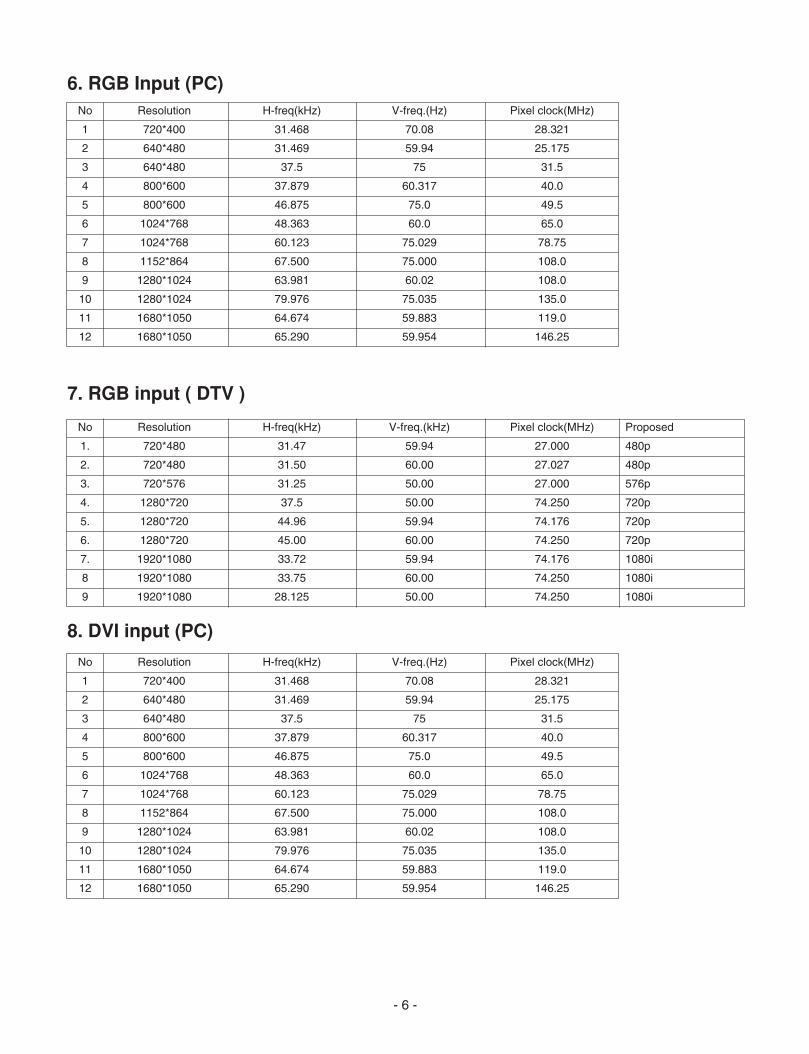
6. RGB Input (PC)No Resolution H-freq(kHz) V-freq.(Hz) Pixel clock(MHz)
1 720*400 31.468 70.08 28.321
2 640*480 31.469 59.94 25.175
3 640*480 37.5 75 31.5
4 800*600 37.879 60.317 40.0
5 800*600 46.875 75.0 49.5
6 1024*768 48.363 60.0 65.0
7 1024*768 60.123 75.029 78.75
8 1152*864 67.500 75.000 108.0
9 1280*1024 63.981 60.02 108.0
10 1280*1024 79.976 75.035 135.0
11 1680*1050 64.674 59.883 119.0
12 1680*1050 65.290 59.954 146.25
No Resolution H-freq(kHz) V-freq.(kHz) Pixel clock(MHz) Proposed
1. 720*480 31.47 59.94 27.000 480p
2. 720*480 31.50 60.00 27.027 480p
3. 720*576 31.25 50.00 27.000 576p
4. 1280*720 37.5 50.00 74.250 720p
5. 1280*720 44.96 59.94 74.176 720p
6. 1280*720 45.00 60.00 74.250 720p
7. 1920*1080 33.72 59.94 74.176 1080i
8 1920*1080 33.75 60.00 74.250 1080i
9 1920*1080 28.125 50.00 74.250 1080i
7. RGB input ( DTV )
8. DVI input (PC)
No Resolution H-freq(kHz) V-freq.(Hz) Pixel clock(MHz)
1 720*400 31.468 70.08 28.321
2 640*480 31.469 59.94 25.175
3 640*480 37.5 75 31.5
4 800*600 37.879 60.317 40.0
5 800*600 46.875 75.0 49.5
6 1024*768 48.363 60.0 65.0
7 1024*768 60.123 75.029 78.75
8 1152*864 67.500 75.000 108.0
9 1280*1024 63.981 60.02 108.0
10 1280*1024 79.976 75.035 135.0
11 1680*1050 64.674 59.883 119.0
12 1680*1050 65.290 59.954 146.25
- 7 -
9. DVI input (DTV)
No Resolution H-freq(kHz) V-freq.(kHz) Pixel clock(MHz) Proposed
1. 720*480 31.47 59.94 27.000 480p
2. 720*480 31.50 60.00 27.027 480p
3. 720*576 31.25 50.00 27.000 576p
4. 1280*720 37.5 50.00 74.250 720p
5. 1280*720 44.96 59.94 74.176 720p
6. 1280*720 45.00 60.00 74.250 720p
7. 1920*1080 33.72 59.94 74.176 1080i
8. 1920*1080 33.75 60.00 74.250 1080i
9. 1920*1080 28.125 50.00 74.250 1080i
- 8 -
WARNING FOR THE SAFETY-RELATED COMPONENT.
• There are some special components used in LCDmonitor that are important for safety. These parts aremarked on the schematic diagram and thereplacement parts list. It is essential that these criticalparts should be replaced with the manufacturer’sspecified parts to prevent electric shock, fire or otherhazard.
• Do not modify original design without obtaining writtenpermission from manufacturer or you will void theoriginal parts and labor guarantee.
TAKE CARE DURING HANDLING THE LCD MODULEWITH BACKLIGHT UNIT.
• Must mount the module using mounting holes arrangedin four corners.
• Do not press on the panel, edge of the frame stronglyor electric shock as this will result in damage to thescreen.
• Do not scratch or press on the panel with any sharpobjects, such as pencil or pen as this may result indamage to the panel.
• Protect the module from the ESD as it may damage theelectronic circuit (C-MOS).
• Make certain that treatment person’s body aregrounded through wrist band.
• Do not leave the module in high temperature and inareas of high humidity for a long time.
• The module not be exposed to the direct sunlight.
• Avoid contact with water as it may a short circuit withinthe module.
• If the surface of panel become dirty, please wipe it offwith a softmaterial. (Cleaning with a dirty or rough clothmay damage the panel.)
WARNING
BE CAREFUL ELECTRIC SHOCK !
• If you want to replace with the new backlight (CCFL) orinverter circuit, must disconnect the AC adapterbecause high voltage appears at inverter circuit about650Vrms.
• Handle with care wires or connectors of the invertercircuit. If the wires are pressed cause short and mayburn or take fire.
Leakage Current Hot Check Circuit
PRECAUTION
CAUTIONPlease use only a plastic screwdriver to protect yourselffrom shock hazard during service operation.
1.5 Kohm/10W
To Instrument'sexposed METALLIC PARTS
Good Earth Groundsuch as WATER PIPE,CONDUIT etc.
AC Volt-meter
- 9 -
SERVICING PRECAUTIONSCAUTION: Before servicing receivers covered by thisservice manual and its supplements and addenda, readand follow the SAFETY PRECAUTIONS on page 3 of thispublication.NOTE: If unforeseen circumstances create conflictbetween the following servicing precautions and any of thesafety precautions on page 3 of this publication, alwaysfollow the safety precautions. Remember: Safety First.
General Servicing Precautions1. Always unplug the receiver AC power cord from the AC
power source before;a. Removing or reinstalling any component, circuit
board module or any other receiver assembly.b. Disconnecting or reconnecting any receiver electrical
plug or other electrical connection.c. Connecting a test substitute in parallel with an
electrolytic capacitor in the receiver.CAUTION: A wrong part substitution or incorrectpolarity installation of electrolytic capacitors mayresult in an explosion hazard.
d. Discharging the picture tube anode.2. Test high voltage only by measuring it with an
appropriate high voltage meter or other voltagemeasuring device (DVM, FETVOM, etc) equipped witha suitable high voltage probe.Do not test high voltage by "drawing an arc".
3. Discharge the picture tube anode only by (a) firstconnecting one end of an insulated clip lead to thedegaussing or kine aquadag grounding system shieldat the point where the picture tube socket ground leadis connected, and then (b) touch the other end of theinsulated clip lead to the picture tube anode button,using an insulating handle to avoid personal contactwith high voltage.
4. Do not spray chemicals on or near this receiver or anyof its assemblies.
5. Unless specified otherwise in this service manual,clean electrical contacts only by applying the followingmixture to the contacts with a pipe cleaner, cotton-tipped stick or comparable non-abrasive applicator;10% (by volume) Acetone and 90% (by volume)isopropyl alcohol (90%-99% strength)CAUTION: This is a flammable mixture.Unless specified otherwise in this service manual,lubrication of contacts in not required.
6. Do not defeat any plug/socket B+ voltage interlockswith which receivers covered by this service manualmight be equipped.
7. Do not apply AC power to this instrument and/or any ofits electrical assemblies unless all solid-state deviceheat sinks are correctly installed.
8. Always connect the test receiver ground lead to thereceiver chassis ground before connecting the testreceiver positive lead.Always remove the test receiver ground lead last.
9. Use with this receiver only the test fixtures specified inthis service manual.CAUTION: Do not connect the test fixture ground strapto any heat sink in this receiver.
Electrostatically Sensitive (ES) DevicesSome semiconductor (solid-state) devices can bedamaged easily by static electricity. Such componentscommonly are called Electrostatically Sensitive (ES)Devices. Examples of typical ES devices are integratedcircuits and some field-effect transistors andsemiconductor "chip" components. The followingtechniques should be used to help reduce the incidence ofcomponent damage caused by static by static electricity.1. Immediately before handling any semiconductor
component or semiconductor-equipped assembly, drainoff any electrostatic charge on your body by touching aknown earth ground. Alternatively, obtain and wear acommercially available discharging wrist strap device,which should be removed to prevent potential shockreasons prior to applying power to the unit under test.
2. After removing an electrical assembly equipped withES devices, place the assembly on a conductivesurface such as aluminum foil, to prevent electrostaticcharge buildup or exposure of the assembly.
3. Use only a grounded-tip soldering iron to solder orunsolder ES devices.
4. Use only an anti-static type solder removal device.Some solder removal devices not classified as "anti-static" can generate electrical charges sufficient todamage ES devices.
5. Do not use freon-propelled chemicals. These cangenerate electrical charges sufficient to damage ESdevices.
6. Do not remove a replacement ES device from itsprotective package until immediately before you areready to install it. (Most replacement ES devices arepackaged with leads electrically shorted together byconductive foam, aluminum foil or comparableconductive material).
7. Immediately before removing the protective materialfrom the leads of a replacement ES device, touch theprotective material to the chassis or circuit assemblyinto which the device will be installed.CAUTION: Be sure no power is applied to the chassisor circuit, and observe all other safety precautions.
8. Minimize bodily motions when handling unpackagedreplacement ES devices. (Otherwise harmless motionsuch as the brushing together of your clothes fabric orthe lifting of your foot from a carpeted floor cangenerate static electricity sufficient to damage an ESdevice.)
- 10 -
General Soldering Guidelines1. Use a grounded-tip, low-wattage soldering iron and
appropriate tip size and shape that will maintain tiptemperature within the range or 500 F to 600 F.
2. Use an appropriate gauge of RMA resin-core soldercomposed of 60 parts tin/40 parts lead.
3. Keep the soldering iron tip clean and well tinned.4. Thoroughly clean the surfaces to be soldered. Use a
mall wire-bristle (0.5 inch, or 1.25cm) brush with ametal handle.Do not use freon-propelled spray-on cleaners.
5. Use the following unsoldering techniquea. Allow the soldering iron t ip to reach normal
temperature.(500 F to 600 F)
b. Heat the component lead until the solder melts.c. Quickly draw the melted solder with an anti-static,
suction-type solder removal device or with solderbraid.CAUTION: Work quickly to avoid overheating thecircuitboard printed foil.
6. Use the following soldering technique.a. Allow the soldering iron tip to reach a normal
temperature (500 F to 600 F)b. First, hold the soldering iron tip and solder the strand
against the component lead until the solder melts.
c. Quickly move the soldering iron tip to the junction ofthe component lead and the printed circuit foil, andhold it there only until the solder flows onto andaround both the component lead and the foil.CAUTION: Work quickly to avoid overheating thecircuit board printed foil.
d. Closely inspect the solder area and remove anyexcess or splashed solder with a small wire-bristlebrush.
IC Remove/ReplacementSome chassis circuit boards have slotted holes (oblong)through which the IC leads are inserted and then bent flatagainst the circuit foil. When holes are the slotted type,the following technique should be used to remove andreplace the IC. When working with boards using thefamiliar round hole, use the standard technique asoutlined in paragraphs 5 and 6 above.
Removal1. Desolder and straighten each IC lead in one operation
by gently prying up on the lead with the soldering irontip as the solder melts.
2. Draw away the melted solder with an anti-staticsuction-type solder removal device (or with solderbraid) before removing the IC.
Replacement1. Carefully insert the replacement IC in the circuit board.2. Carefully bend each IC lead against the circuit foil pad
and solder it.3. Clean the soldered areas with a small wire-bristle
brush. (It is not necessary to reapply acrylic coating tothe areas).
"Small-Signal" Discrete TransistorRemoval/Replacement1. Remove the defective transistor by clipping its leads as
close as possible to the component body.2. Bend into a "U" shape the end of each of three leads
remaining on the circuit board.3. Bend into a "U" shape the replacement transistor leads.4. Connect the replacement transistor leads to the
corresponding leads extending from the circuit boardand crimp the "U" with long nose pliers to insure metalto metal contact then solder each connection.
Power Output, Transistor DeviceRemoval/Replacement1. Heat and remove all solder from around the transistor
leads.2. Remove the heat sink mounting screw (if so equipped).3. Carefully remove the transistor from the heat sink of the
circuit board.4. Insert new transistor in the circuit board.5. Solder each transistor lead, and clip off excess lead.6. Replace heat sink.
Diode Removal/Replacement1. Remove defective diode by clipping its leads as close
as possible to diode body.2. Bend the two remaining leads perpendicular y to the
circuit board.3. Observing diode polarity, wrap each lead of the new
diode around the corresponding lead on the circuitboard.
4. Securely crimp each connection and solder it.5. Inspect (on the circuit board copper side) the solder
joints of the two "original" leads. If they are not shiny,reheat them and if necessary, apply additional solder.
Fuse and Conventional ResistorRemoval/Replacement1. Clip each fuse or resistor lead at top of the circuit board
hollow stake.2. Securely crimp the leads of replacement component
around notch at stake top.3. Solder the connections.
CAUTION: Maintain original spacing between thereplaced component and adjacent components and thecircuit board to prevent excessive componenttemperatures.
- 11 -
Circuit Board Foil RepairExcessive heat applied to the copper foil of any printedcircuit board will weaken the adhesive that bonds the foilto the circuit board causing the foil to separate from or"l i f t-off" the board. The following guidelines andprocedures should be followed whenever this condition isencountered.
At IC ConnectionsTo repair a defective copper pattern at IC connections usethe following procedure to install a jumper wire on thecopper pattern side of the circuit board. (Use thistechnique only on IC connections).
1. Carefully remove the damaged copper pattern with asharp knife. (Remove only as much copper asabsolutely necessary).
2. carefully scratch away the solder resist and acryliccoating (if used) from the end of the remaining copperpattern.
3. Bend a small "U" in one end of a small gauge jumperwire and carefully crimp it around the IC pin. Solder theIC connection.
4. Route the jumper wire along the path of the out-awaycopper pattern and let it overlap the previously scrapedend of the good copper pattern. Solder the overlappedarea and clip off any excess jumper wire.
At Other ConnectionsUse the following technique to repair the defective copperpattern at connections other than IC Pins. This techniqueinvolves the installation of a jumper wire on thecomponent side of the circuit board.1. Remove the defective copper pattern with a sharp
knife.Remove at least 1/4 inch of copper, to ensure that ahazardous condition will not exist if the jumper wireopens.
2. Trace along the copper pattern from both sides of thepattern break and locate the nearest component that isdirectly connected to the affected copper pattern.
3. Connect insulated 20-gauge jumper wire from the leadof the nearest component on one side of the patternbreak to the lead of the nearest component on theother side.Carefully crimp and solder the connections.CAUTION: Be sure the insulated jumper wire isdressed so the it does not touch components or sharpedges.
DISASSEMBLY
- 12 -
1. Push down slightly to disassembly it.
2. After push the cable management like above fig.(Downward),
Disassembly the Cable management with pulling it upward.
3. Disassembly Cable Holder.
Disassembly stand base.
Remove base body Like a picture. Push 2 letches Like a picture.
Push the button.
Hold the stand base.
# 1
# 4
# 2
# 5
# 3
# 6
- 13 -
# 7
# 9
# 8
# 10
Pull base body to separate from set during pressing 2 letches.
Remove the screws.
# 11
Pull the connector.
Disassembly back cover.
1. Remove the screws.
2. Disassembly Hinge Cover.
- 14 -
DV
I-D
CV
BS
SP
(R
)
SP
(L)
Aud
ioA
mp
(YD
A13
8)
LCD
Mod
ule
(AU
O)
16M
b S
DR
AM
(HY
57V
1616
10F
TP
)
EE
PR
OM
Sys
tem
(64k
)
Y/C
Dat
a(F
SD
0 ..
31)
(FS
A 0
..11
)
Y/P
b/P
r4M
b S
eria
lF
lash
Mem
ory
(MX
25L4
005A
)
Dat
a(O
CM
D 0
..7)
(OC
MA
0 ..
19)
Ana
log
Sig
nal
(R/G
/B/H
/V)
TM
DS
Sig
nal
CO
MP
PC
Aud
io
CO
MP
Aud
io
CV
BS
Aud
io
EE
PR
OM
D-S
UB
EE
PR
OM
Tune
rTA
FT-
W00
3D
CV
BS
SIF
L R
LV
DS
Sig
nal
L/R
Sca
ler+
Vid
eo
Dec
orde
r
(LG
E97
89A
D-L
F)
R/G
/B/C
VB
S/A
udio
SC
AR
T
CV
BS
/Aud
io
L/R
L/R
CS
4351
(DA
C)
INP
UT
ME
NU
OK
VO
LP
R
PO
WE
RIR
EA
GLE
EY
E
BLOCK DIAGRAM
- 15 -
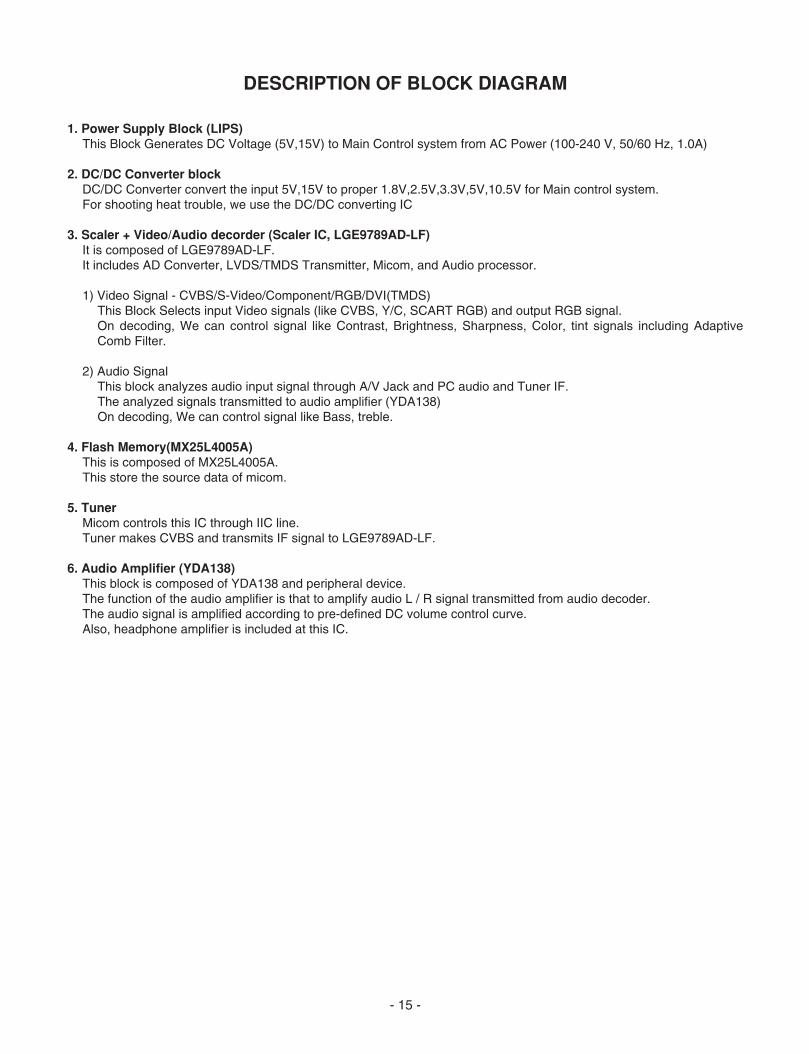
DESCRIPTION OF BLOCK DIAGRAM
1. Power Supply Block (LIPS)This Block Generates DC Voltage (5V,15V) to Main Control system from AC Power (100-240 V, 50/60 Hz, 1.0A)
2. DC/DC Converter block DC/DC Converter convert the input 5V,15V to proper 1.8V,2.5V,3.3V,5V,10.5V for Main control system.For shooting heat trouble, we use the DC/DC converting IC
3. Scaler + Video/Audio decorder (Scaler IC, LGE9789AD-LF)It is composed of LGE9789AD-LF.It includes AD Converter, LVDS/TMDS Transmitter, Micom, and Audio processor.
1) Video Signal - CVBS/S-Video/Component/RGB/DVI(TMDS)This Block Selects input Video signals (like CVBS, Y/C, SCART RGB) and output RGB signal.On decoding, We can control signal like Contrast, Brightness, Sharpness, Color, tint signals including AdaptiveComb Filter.
2) Audio SignalThis block analyzes audio input signal through A/V Jack and PC audio and Tuner IF.The analyzed signals transmitted to audio amplifier (YDA138)On decoding, We can control signal like Bass, treble.
4. Flash Memory(MX25L4005A)This is composed of MX25L4005A.This store the source data of micom.
5. TunerMicom controls this IC through IIC line.Tuner makes CVBS and transmits IF signal to LGE9789AD-LF.
6. Audio Amplifier (YDA138)This block is composed of YDA138 and peripheral device.The function of the audio amplifier is that to amplify audio L / R signal transmitted from audio decoder. The audio signal is amplified according to pre-defined DC volume control curve.Also, headphone amplifier is included at this IC.
- 16 -
EMICOMPONENTS
LINE100 ~ 240V
INPUT RECTIFIERAND FILTER
ENERGYTRANSFER
OUTPUT RECTIFIERAND FILTER
15V
5V
GND
SIGNALCOLLENT-
ION
PHOTO-COUPLERISOLATION
HVDC 100KHz
PRIMARY SECONDARY
50 ~ 60Hz
PWMCONTROLCIRCUIT
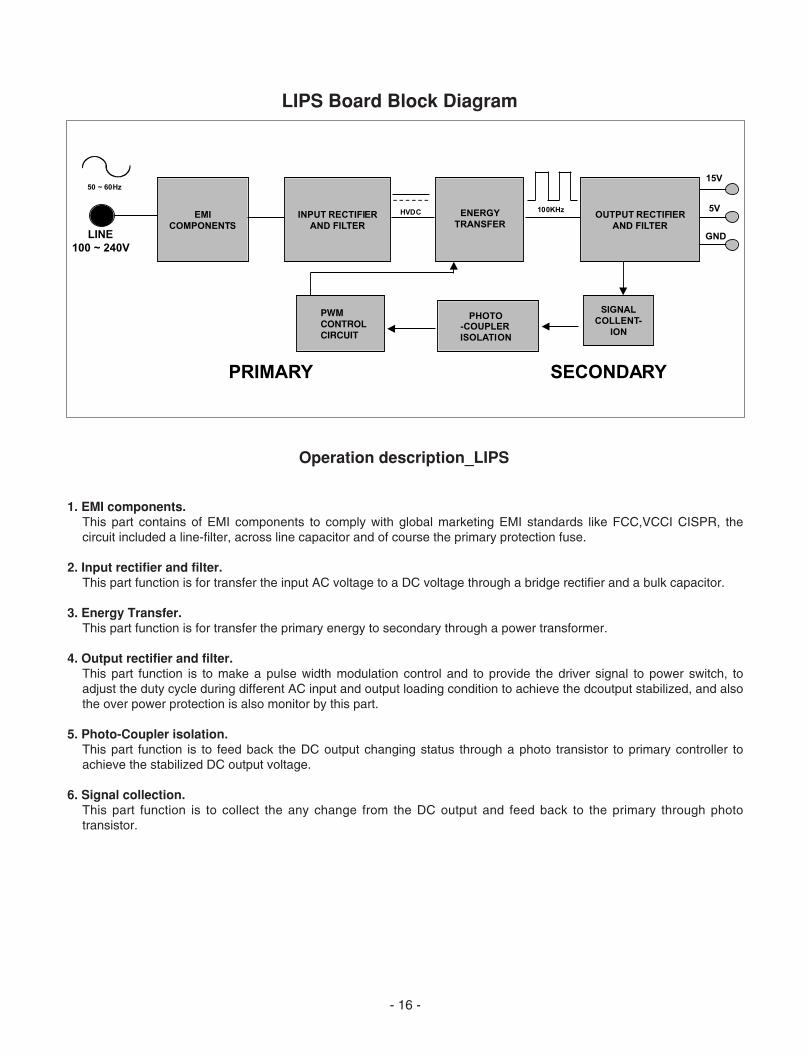
LIPS Board Block Diagram
Operation description_LIPS
1. EMI components.This part contains of EMI components to comply with global marketing EMI standards like FCC,VCCI CISPR, thecircuit included a line-filter, across line capacitor and of course the primary protection fuse.
2. Input rectifier and filter.This part function is for transfer the input AC voltage to a DC voltage through a bridge rectifier and a bulk capacitor.
3. Energy Transfer.This part function is for transfer the primary energy to secondary through a power transformer.
4. Output rectifier and filter.This part function is to make a pulse width modulation control and to provide the driver signal to power switch, toadjust the duty cycle during different AC input and output loading condition to achieve the dcoutput stabilized, and alsothe over power protection is also monitor by this part.
5. Photo-Coupler isolation.This part function is to feed back the DC output changing status through a photo transistor to primary controller toachieve the stabilized DC output voltage.
6. Signal collection.This part function is to collect the any change from the DC output and feed back to the primary through phototransistor.
- 17 -
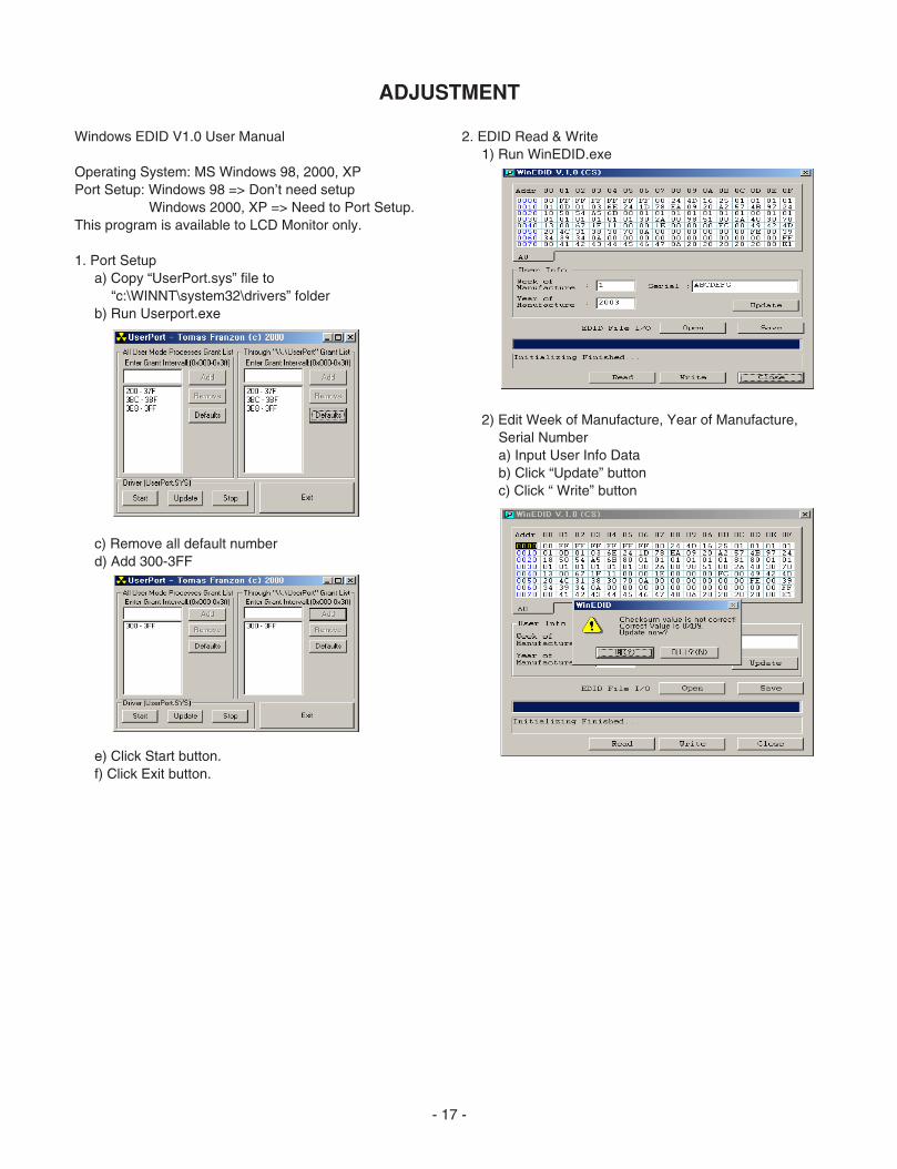
ADJUSTMENT
Windows EDID V1.0 User Manual
Operating System: MS Windows 98, 2000, XPPort Setup: Windows 98 => Don’t need setup
Windows 2000, XP => Need to Port Setup.This program is available to LCD Monitor only.
1. Port Setupa) Copy “UserPort.sys” file to
“c:\WINNT\system32\drivers” folderb) Run Userport.exe
c) Remove all default numberd) Add 300-3FF
e) Click Start button.f) Click Exit button.
2. EDID Read & Write1) Run WinEDID.exe
2) Edit Week of Manufacture, Year of Manufacture, Serial Numbera) Input User Info Datab) Click “Update” buttonc) Click “ Write” button
- 18 -
ADJUSTMENT INSTRUCTION
1. Application RangeThis specification sheet is applied to 19"/ 20"/ 22" LCDMonitor TV which is manufactured in TV (or Monitor) Factoryor is produced on the basis of this data.
2. Specification1) The adjustment is according to the order which is
designated and which must be followed, according to theplan which can be changed only on agreeing.
2) Power Adjustment : Free Voltage3) Magnetic Field Condition : Nil.4) Input signal Unit : Product Specification Standard5) Reserve after operation : Above 30 Minutes 6) Adjustment equipments : Color Analyzer(CA-210 or CA-
110), Pattern Generator (MSPG-925L or Equivalent), DDCAdjustment Jig equipment, SVC remote controller
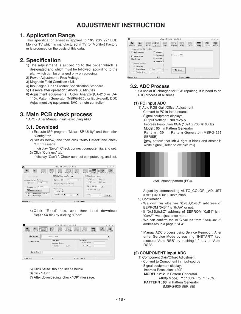
3. Main PCB check process* APC - After Manual-Insult, executing APC
3.1. Download1) Execute ISP program “Mstar ISP Utility” and then click
“Config” tab.2) Set as below, and then click “Auto Detect” and check
“OK” message.If display “Error”, Check connect computer, jig, and set.
3) Click “Connect” tab.If display “Can’t ”, Check connect computer, jig, and set.
4) Click “Read” tab, and then load downloadfile(XXXX.bin) by clicking “Read”.
5) Click “Auto” tab and set as below6) click “Run”.7) After downloading, check “OK” message.
3.2. ADC Process* If a scaler IC changed for PCB repairing, it is need to do
ADC process at all times.
(1) PC input ADC1) Auto RGB Gain/Offset Adjustment
- Convert to PC in Input-source- Signal equipment displays
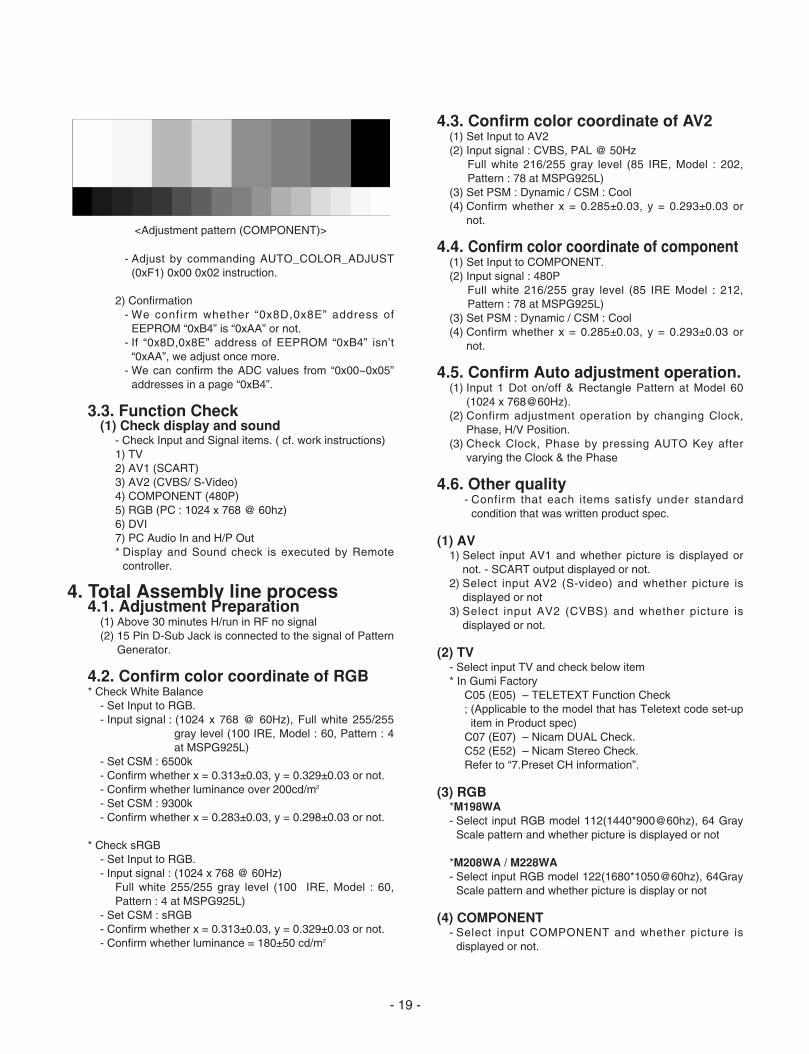
Output Voltage : 700 mVp-pImpress Resolution XGA (1024 x 768 @ 60Hz)Model : 60 in Pattern GeneratorPattern : 29 in Pattern Generator (MSPG-925SERISE) [gray pattern that left & right is black and center iswhite signal (Refer below picture)].
- Adjust by commanding AUTO_COLOR _ADJUST(0xF1) 0x00 0x02 instruction.
2) Confirmation- We confirm whether “0x8B,0x8C” address of
EEPROM “0xB4” is “0xAA” or not.- If “0x8B,0x8C” address of EEPROM “0xB4” isn’t
“0xAA”, we adjust once more.- We can confirm the ADC values from “0x00~0x05”
addresses in a page “0xB4”
* Manual ADC process using Service Remocon. Afterenter Service Mode by pushing “INSTART” key,execute “Auto-RGB” by pushing “_” key at “Auto-RGB”.
(2) COMPONENT input ADC1) Component Gain/Offset Adjustment
- Convert to Component in Input-source- Signal equipment displays
Impress Resolution 480PMODEL : 212 in Pattern Generator
(480p Mode, Y : 100%, Pb/Pr : 75%)PATTERN : 08 in Pattern Generator
(MSPG-925 SERISE)
<Adjustment pattern (PC)>
- 19 -
<Adjustment pattern (COMPONENT)>
- Adjust by commanding AUTO_COLOR_ADJUST(0xF1) 0x00 0x02 instruction.
2) Confirmation- We confirm whether “0x8D,0x8E” address of
EEPROM “0xB4” is “0xAA” or not.- If “0x8D,0x8E” address of EEPROM “0xB4” isn’t
“0xAA”, we adjust once more.- We can confirm the ADC values from “0x00~0x05”
addresses in a page “0xB4”.
3.3. Function Check(1) Check display and sound
- Check Input and Signal items. ( cf. work instructions)1) TV2) AV1 (SCART)3) AV2 (CVBS/ S-Video)4) COMPONENT (480P)5) RGB (PC : 1024 x 768 @ 60hz)6) DVI7) PC Audio In and H/P Out* Display and Sound check is executed by Remote
controller.
4. Total Assembly line process4.1. Adjustment Preparation
(1) Above 30 minutes H/run in RF no signal (2) 15 Pin D-Sub Jack is connected to the signal of Pattern
Generator.
4.2. Confirm color coordinate of RGB* Check White Balance
- Set Input to RGB.- Input signal : (1024 x 768 @ 60Hz), Full white 255/255
gray level (100 IRE, Model : 60, Pattern : 4at MSPG925L)
- Set CSM : 6500k- Confirm whether x = 0.313±0.03, y = 0.329±0.03 or not. - Confirm whether luminance over 200cd/m2
- Set CSM : 9300k - Confirm whether x = 0.283±0.03, y = 0.298±0.03 or not.
* Check sRGB- Set Input to RGB.- Input signal : (1024 x 768 @ 60Hz)
Full white 255/255 gray level (100 IRE, Model : 60,Pattern : 4 at MSPG925L)
- Set CSM : sRGB - Confirm whether x = 0.313±0.03, y = 0.329±0.03 or not. - Confirm whether luminance = 180±50 cd/m2
4.3. Confirm color coordinate of AV2(1) Set Input to AV2(2) Input signal : CVBS, PAL @ 50Hz
Full white 216/255 gray level (85 IRE, Model : 202,Pattern : 78 at MSPG925L)
(3) Set PSM : Dynamic / CSM : Cool(4) Confirm whether x = 0.285±0.03, y = 0.293±0.03 or
not.
4.4. Confirm color coordinate of component(1) Set Input to COMPONENT.(2) Input signal : 480P
Full white 216/255 gray level (85 IRE Model : 212,Pattern : 78 at MSPG925L)
(3) Set PSM : Dynamic / CSM : Cool(4) Confirm whether x = 0.285±0.03, y = 0.293±0.03 or
not.
4.5. Confirm Auto adjustment operation.(1) Input 1 Dot on/off & Rectangle Pattern at Model 60
(1024 x 768@60Hz).(2) Confirm adjustment operation by changing Clock,
Phase, H/V Position.(3) Check Clock, Phase by pressing AUTO Key after
varying the Clock & the Phase
4.6. Other quality - Confirm that each items satisfy under standard
condition that was written product spec.
(1) AV1) Select input AV1 and whether picture is displayed or
not. - SCART output displayed or not.2) Select input AV2 (S-video) and whether picture is
displayed or not3) Select input AV2 (CVBS) and whether picture is
displayed or not.
(2) TV- Select input TV and check below item * In Gumi Factory
C05 (E05) – TELETEXT Function Check ; (Applicable to the model that has Teletext code set-upitem in Product spec)
C07 (E07) – Nicam DUAL Check.C52 (E52) – Nicam Stereo Check.Refer to “7.Preset CH information”.
(3) RGB*M198WA- Select input RGB model 112(1440*900@60hz), 64 Gray
Scale pattern and whether picture is displayed or not
*M208WA / M228WA- Select input RGB model 122(1680*1050@60hz), 64Gray
Scale pattern and whether picture is display or not
(4) COMPONENT- Select input COMPONENT and whether picture is
displayed or not.
(5) DVI*M198WA- Select input DVI model 112(1440*900@60hz), 64 Gray
Scale pattern and whether picture is displayed or not
*M208WA / M228WA- Select input DVI model 122(1680*1050@60hz), 64Gray
pattern and whether picture is displayed or not.
4.7. DPM operation confirmation- Check if Power LED Color and Power Consumption operate
as standard. (1) Set Input to RGB and connect D-sub cable to set.(2) Measurement Condition : 230V@ 50Hz (Analog)(3) Confirm DPM operation at the state of screen without
Signal
4.8 DDC EDID Write1) Connect D-sub Signal Cable to D-Sub Jack.2) Connect HDMI Signal Cable to HDMI Jack.3) Write EDID DATA to EEPROM(24C02) by using DDC2B
protocol.4) Check whether written EDID data is correct or not. (refer
to Product spec).
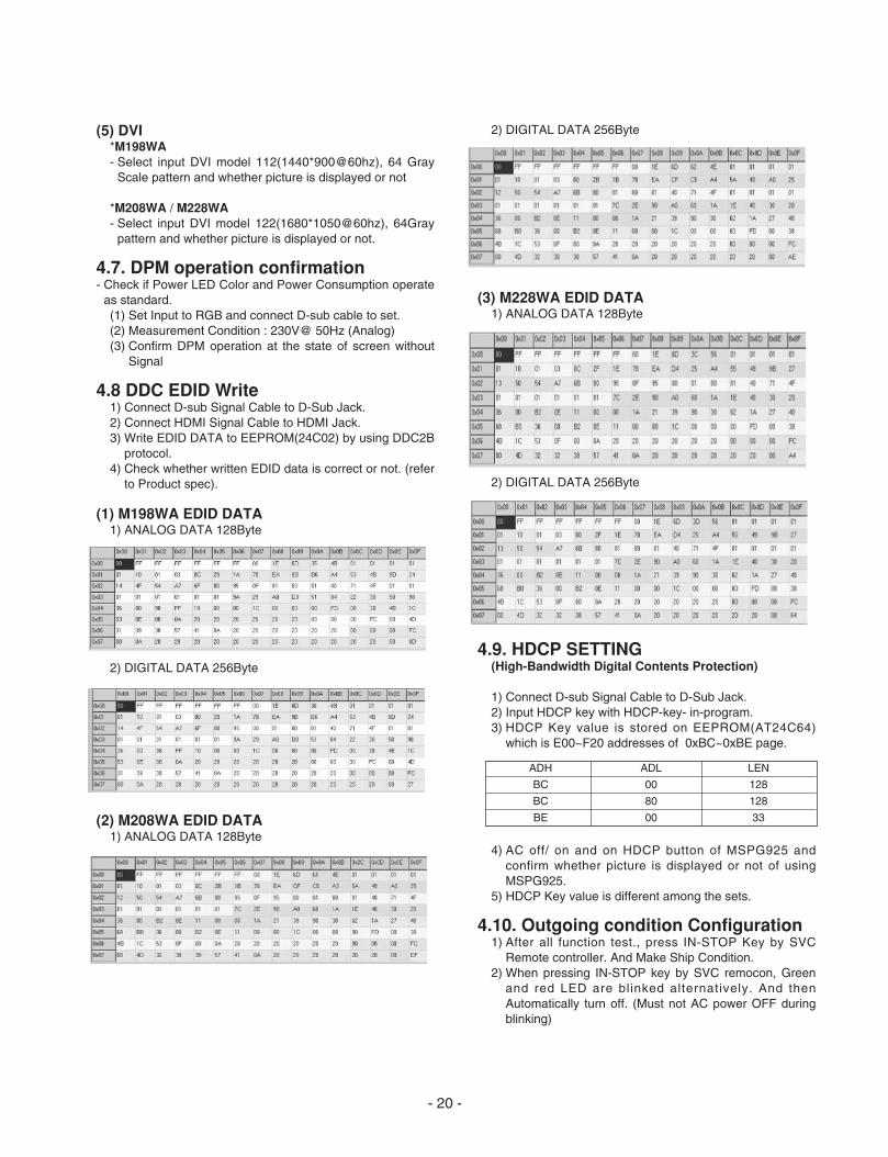
(1) M198WA EDID DATA1) ANALOG DATA 128Byte
2) DIGITAL DATA 256Byte
(2) M208WA EDID DATA1) ANALOG DATA 128Byte
2) DIGITAL DATA 256Byte
(3) M228WA EDID DATA1) ANALOG DATA 128Byte
2) DIGITAL DATA 256Byte
4.9. HDCP SETTING(High-Bandwidth Digital Contents Protection)
1) Connect D-sub Signal Cable to D-Sub Jack.2) Input HDCP key with HDCP-key- in-program.3) HDCP Key value is stored on EEPROM(AT24C64)
which is E00~F20 addresses of 0xBC~0xBE page.
4) AC off/ on and on HDCP button of MSPG925 andconfirm whether picture is displayed or not of usingMSPG925.
5) HDCP Key value is different among the sets.
4.10. Outgoing condition Configuration1) After all function test., press IN-STOP Key by SVC
Remote controller. And Make Ship Condition. 2) When pressing IN-STOP key by SVC remocon, Green
and red LED are blinked alternatively. And thenAutomatically turn off. (Must not AC power OFF duringblinking)
- 20 -
ADH ADL LEN
BC 00 128
BC 80 128
BE 00 33
- 21 -
4.11. Internal pressure- Confirm whether is nomal or not when between power
board's ac block and GND is impacked on 1.5kV(dc) or2.2kV(dc) for one second.
4.12 Option data setting (SVC OSD setting) (1) PAL Model
*M198WA(Change by Suffix) Tool Option 8065
*M208WA/M228WA(Change by Suffix) Tool Option 8066
*M198WA/M208WA/M228WA(Change by Suffix) Area Option 00
Option1(6)
1 200PR 0 0 : 200 PR Off
1 : 200 PR On
2 ACMS 1 0 : ACMS Off
1 : ACMS On
3 Text 1 TOP
FLOF
4 CH+AU 0 0 : Except below area
1 : China, Australia
5 BOOSTER 0
Option2(2)
1 SYS 0 0 : BG/I/DK/L
1 : BG/I/DK/M
2 A2 ST 1 Acting FM-ST after checking
Nicam
3 I II SAVE 0 0 : I II SAVE Off
1 : I II SAVE On
4 HDEV 0 0 : Except below area
1 : China
5 V-Curve 0 0 : Turbo Volume Off
1 : Turbo Volume On
6 MONO 0
Option3(2)
1 KEY-TYPE 2 2 : 8Key
Option 4(3)
1 Default Lang (Language) 3
2 Lang 0 Chesky,Dansk,Deutsch,English
Español,Français,Italiano,
Magyar,Nederlands,Norsk,
Polski,Português,
Romaneste,Suomi,Svenska
3 T- Lang 0 AUSTRIA,BULGARIA,
CROATIA,CZECH, DENMARK,
ESTONIA,FINLAND,FRANCE,
GERMANY,GREECE,
HUNGARY,ITALY,LATVIA,
NETHERLANDS,NORWAY,
POLAND,PORTUGAL,
RUMANIA,RUSSIA,SERBIA,
SLOVAKIA,SLOVENIA,SPAIN,
SWEDEN,SWITZERLAND,
TURKEY,UK,ARAB,HEBREW,
Others
Option5(9)
1 2HR-OFF 1 0 : 2 Hour off option -OFF
1 : 2 Hour off option -ON
2 TV-LINK-TUNER 0
3 FACTORY-MODE 0 0 : EEPROM Write Protection On
1 : EEPROM Write Protection Off
4 CHANNEL-MUTE 1
No. Item Condition Remark
M198WA-BZH REMARK
Resolution 1 WXGA+
Module 0
TV 1
SCART 1
AV2 1
COMPONENT 1
PC-RGB 1
DVI 1
HDMI 0
M208WA-BZH / M228WA-BZH REMARK
Resolution 2 WSXGA
Module 0
TV 1
SCART 1
AV2 1
COMPONENT 1
PC-RGB 1
DVI 1
HDMI 0
- 22 -
5. Adjustment Command5.1. Adjustment Commands(LENGTH=84)
5.2 EEPROM DATA READ(1) Signal Table
(2) Command Set
* Purpose : To read the appointment Address ofE2PROM by 128(80h)-byte
5.3. E2PROM Data Write(1) Signal Table
LEN : 84h+BytesCMD : 8EhADH : E2PROM Slave Address(A0,A2,A4,A6,A8), Not
00h(Reserved by BufferToEEPROM)ADL : E2PROM Sub Address(00~FF)Data : Write data
(2) Command Set
* Purpose1) EDID write : 16-byte by 16-byte, 8 order (128-byte)
write(TO “00 – 7F” of “EEPROM Page A4”).2) FOS Default write : 16-mode data (HFh, HFl, VF, STD,
HP, VP, Clk, ClkPh, PhFine) write.3) Random Data write : write the appointment Address of
E2PROM.
5.4. VRAM Read1) Send CMD(70h) to read Video RAM value from MICOM
And save its value to 128-Bytes Buffer(Common Bufferfor the use of EDID)
2) Delay 500ms ( Time to Wait and Read Video RAM fromMICOM)
3) Be transmitted the contents of MICOM’s 128-bytesBuffer to PC. (128th Data is the CheckSum of 127-bytesdata : That’s OK if the value of adding 128-bytes Data isZero)
FACTORY ON E0 00 00 Factory mode on
FACTORY OFF E2 00 00 Factory mode off
EEPROM ALL INIT. E4 00 00 EEPROM All clear
EEPROM Read E7 00 00 EEPROM Read
EEPROM Write E8 00 data EEPROM Write by some
values
COLOR SAVE
(R/G/B cutoff, Drive, EB 00 00 Color Save
Contrast, Bright)
H POSITION 20 00 00 – 100 They have different range
V POSITION 30 00 00 – 100 each mode, FOS Adjustment
CLOCK 90 00 00 – 100
PHASE 92 00 00 – 100
R DRIVE 16 00 00 – FF Drive adjustment
G DRIVE 18 00 00 – FF
B DRIVE 1A 00 00 – FF
R CUTOFF 80 00 00 – 7F Offset adjustment
G CUTOFF 82 00 00 – 7F
B CUTOFF 84 00 00 – 7F
BRIGHT 10 00 00 – 3F Bright adjustment
CONTRAST 12 00 00 - 64 Luminance adjustment
AUTO_COLOR_ F1 00 02 Auto COLOR Adjustment
ADJUST
CHANGE_COLOR F2 00 0,1,2,3 0: COOL
_TEMP 1: NORMAL
2: WARM
3: USER
FACTORY_DEFAULT F3 00 00 Factory mode off
& II_SW is “1”
& Input change to “ TV”
AUTO_INPUT F4 00 0,1,2,4 0 : TV
CHANGE 1 : AV1
2 : AV2
3 : Component
4 : RGB
5 : DVI
ADR VAL DescriptionCMD(hex)
Adjustment Contents
128 Bytes
Delay 100ms
EEPROM READ E7 A0 0 0-Page 0~7F Read
80 0-Page 80~FF Read
A2 0 1-Page 0~7F Read
80 1-Page 80~FF Read
A4 0 2-Page 0~7F Read
80 2-Page 80~FF Read
A6 0 3-Page 0~7F Read
80 3-Page 80~FF Read
Adjustment contents CMD(hex) ADH(hex) ADL(hex) Details
EEPROM WRITE E8 94 16-Byte Write
84+n n-byte Write
Adjustment contents CMD(hex) ADH(hex) Details
- 23 -
Figure 1. Cable Connection
220
IBMCompatible PC
PARALLEL PORT
Power inlet (required)
Power LED
ST Switch
Power Select Switch(110V/220V)
Con
trol
Lin
e
Not u
sed
RS232
C
PARAL
LEL
V-SY
NC
POW
ER
ST
VGS
MONITOR
E
E
V-Sync On/Off Switch(Switch must be ON.)
F
F
A
A
BB
C
C
15105
5
69
1
1
1
14
13
25
6
5V
5V
5V
4.7K4.7K
4.7K
74LS06
74LS06
OFF ON
OFF
ON
11Video SignalGenerator
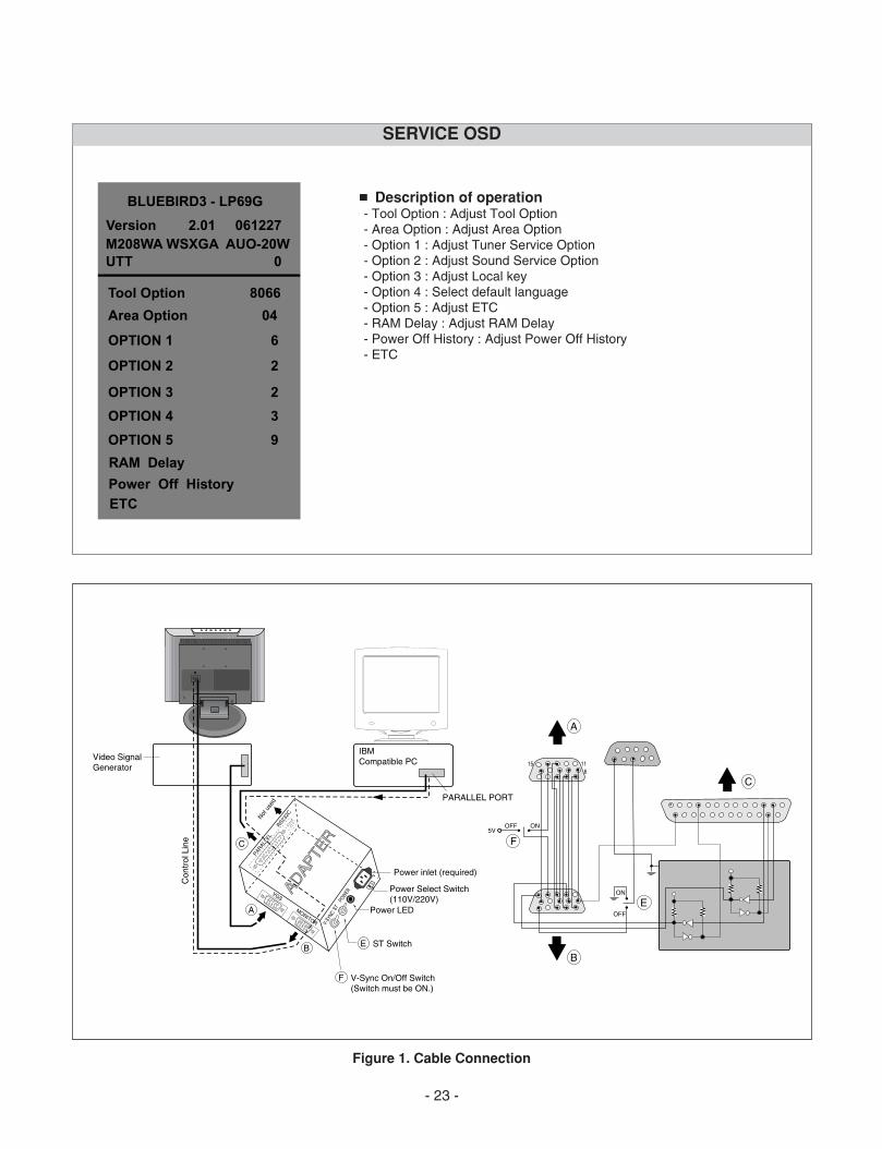
SERVICE OSD
Tool Option 8066
Area Option 04
OPTION 1 6
RAM Delay
OPTION 2 2
OPTION 3 2
OPTION 4 3
OPTION 5 9
ETC
BLUEBIRD3 - LP69G
Version 2.01 061227
UTT M208WA WSXGA AUO-20W
0
Power Off History
Description of operation- Tool Option : Adjust Tool Option- Area Option : Adjust Area Option- Option 1 : Adjust Tuner Service Option- Option 2 : Adjust Sound Service Option- Option 3 : Adjust Local key- Option 4 : Select default language- Option 5 : Adjust ETC- RAM Delay : Adjust RAM Delay- Power Off History : Adjust Power Off History- ETC
- 24 -
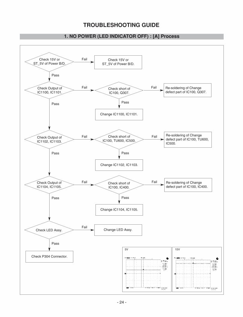
TROUBLESHOOTING GUIDE
1. NO POWER (LED INDICATOR OFF) : [A] Process
Check 15V orST_5V of Power B/D.
Fail Check 15V orST_5V of Power B/D.
Check Output ofIC1100, IC1101.
Check short ofIC100, Q307.
Pass
Pass
Pass
Pass
Re-soldering of Changedefect part of IC100, Q307.
Change IC1100, IC1101.
Change IC1102, IC1103.
Check Output ofIC1102, IC1103.
Check short ofIC100, TU600, IC500.
Re-soldering of Changedefect part of IC100, TU600,IC500.
Change IC1104, IC1105.
Change LED Assy.
Check Output ofIC1104, IC1105.
Check LED Assy.
Check P304 Connector.
Check short ofIC100, IC400.
Re-soldering of Changedefect part of IC100, IC400.
Fail
Fail
Fail
Fail
Fail
Fail
Fail
Pass
Pass
Pass
Pass
5V 15V
- 25 -
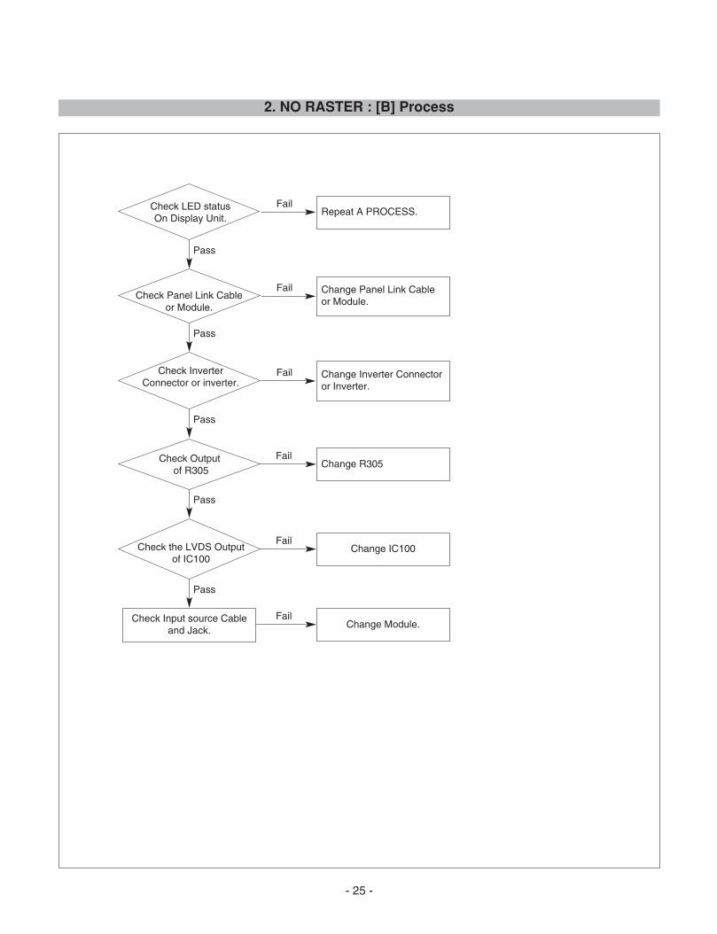
2. NO RASTER : [B] Process
Check LED statusOn Display Unit.
FailRepeat A PROCESS.
FailCheck Panel Link Cable
or Module.
Change Panel Link Cableor Module.
Check InverterConnector or inverter.
Change Inverter Connectoror Inverter.
Change IC100
Check Outputof R305
Check the LVDS Outputof IC100
Check Input source Cableand Jack.
Change Module.
Change R305
Pass
Pass
Pass
Pass
Pass
Fail
Fail
Fail
Fail
- 26 -
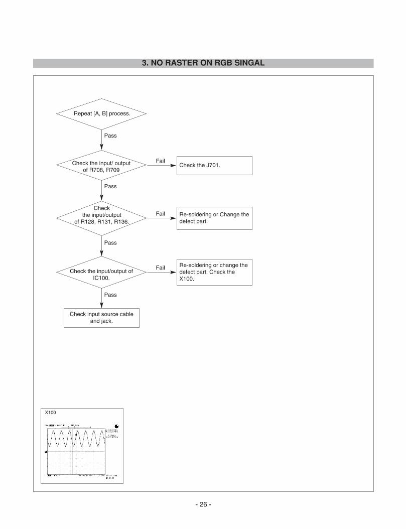
3. NO RASTER ON RGB SINGAL
Repeat [A, B] process.
Check the input/ outputof R708, R709
FailCheck the J701.
Fail
Fail Re-soldering or change thedefect part, Check theX100.
Checkthe input/output
of R128, R131, R136.
Check the input/output ofIC100.
Check input source cableand jack.
Re-soldering or Change thedefect part.
Pass
Pass
Pass
Pass
X100
- 27 -
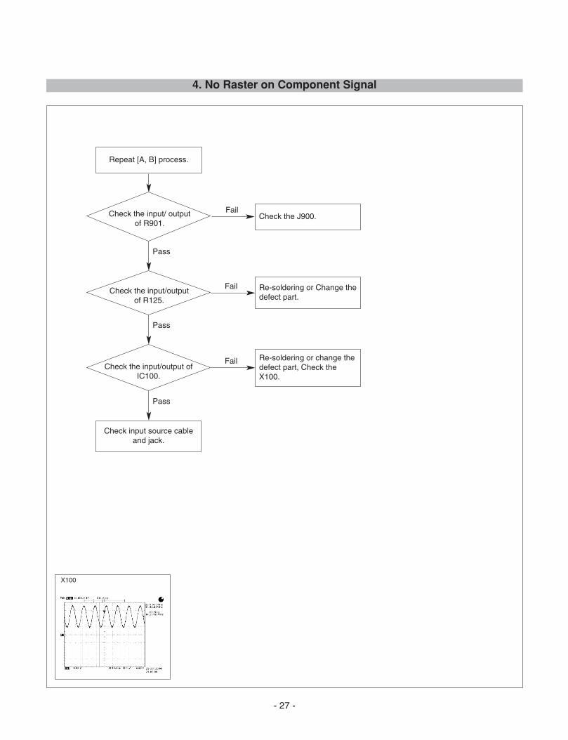
4. No Raster on Component Signal
Repeat [A, B] process.
Check the input/ outputof R901.
FailCheck the J900.
Fail
Pass
Re-soldering or change thedefect part, Check theX100.
Check the input/outputof R125.
Check the input/output ofIC100.
Check input source cableand jack.
Re-soldering or Change thedefect part.
Pass
Pass
Fail
X100
- 28 -
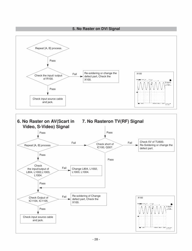
5. No Raster on DVI Signal
Repeat [A, B] process.
Pass
Check the input/ outputof R100.
Fail Re-soldering or change thedefect part, Check theX100.
Check input source cableand jack.
Pass
6. No Raster on AV(Scart inVideo, S-Video) Signal
7. No Rasteron TV(RF) Signal
Check input source cableand jack.
Repeat [A, B] process.Fail Check short of
IC100, Q307.
Fail
Fail
Fail
Pass
Check 5V of TU600.Re-Soldering or change thedefect part.
Checkthe input/output of
L804, L1002,L1003,L1004.
Change L804, L1002,L1003, L1004.
Check Output ofIC1104, IC1105.
Re-soldering of Changedefect part, Check theX100.
Pass Pass
Pass
Pass
Pass
X100
X100
- 29 -
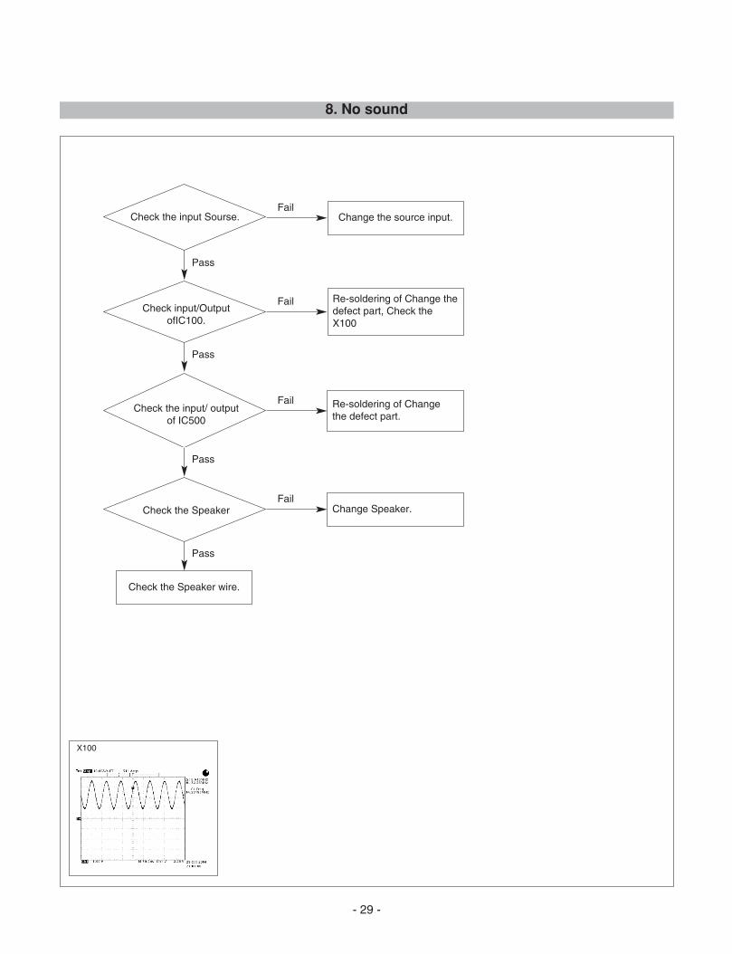
8. No sound
Check the input Sourse.Fail
Pass
Change the source input.
Check input/OutputofIC100.
Pass
Re-soldering of Change thedefect part, Check theX100
Check the input/ outputof IC500
Re-soldering of Changethe defect part.
Check the Speaker
Check the Speaker wire.
Change Speaker.
Pass
Pass
Fail
Fail
Fail
X100
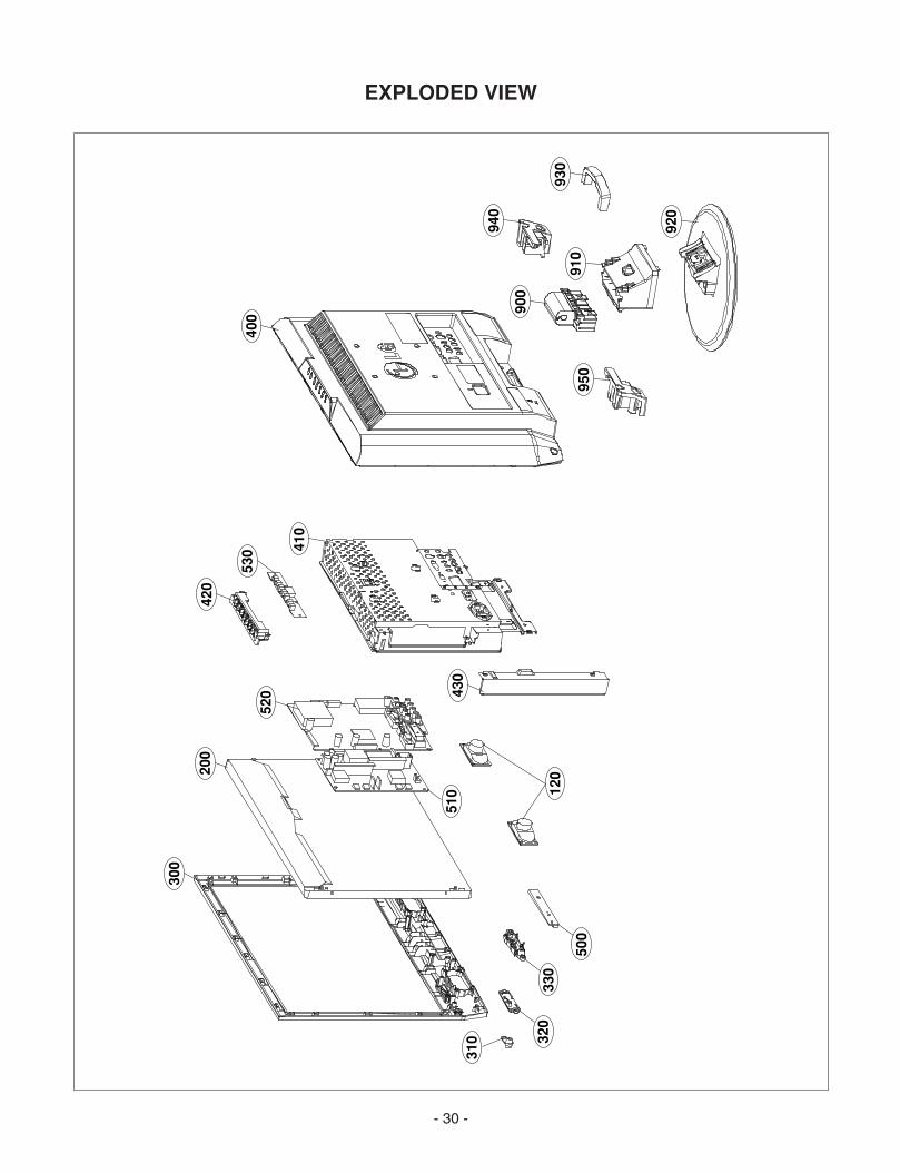
EXPLODED VIEW
- 30 -
300
200
120
510
320
330
500
310
520
420
430
530 41
0
400
940
900
950
910
930
920
- 31 -
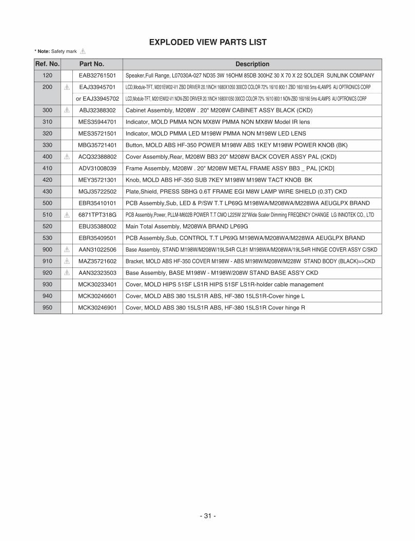
EXPLODED VIEW PARTS LIST
120
200
300
310
320
330
400
410
420
430
500
510
520
530
900
910
920
930
940
950
EAB32761501 Speaker,Full Range, L07030A-027 ND35 3W 16OHM 85DB 300HZ 30 X 70 X 22 SOLDER SUNLINK COMPANY
EAJ33945701 LCD,Module-TFT, M201EW02-V1 ZBD DRIVER 20.1INCH 1680X1050 300CD COLOR 72% 16/10 800:1 ZBD 160/160 5ms 4LAMPS AU OPTRONICS CORP
or EAJ33945702 LCD,Module-TFT, M201EW02-V1 NON-ZBD DRIVER 20.1INCH 1680X1050 300CD COLOR 72% 16/10 800:1 NON-ZBD 160/160 5ms 4LAMPS AU OPTRONICS CORP
ABJ32388302 Cabinet Assembly, M208W . 20" M208W CABINET ASSY BLACK (CKD)
MES35944701 Indicator, MOLD PMMA NON MX8W PMMA NON MX8W Model IR lens
MES35721501 Indicator, MOLD PMMA LED M198W PMMA NON M198W LED LENS
MBG35721401 Button, MOLD ABS HF-350 POWER M198W ABS 1KEY M198W POWER KNOB (BK)
ACQ32388802 Cover Assembly,Rear, M208W BB3 20" M208W BACK COVER ASSY PAL (CKD)
ADV31008039 Frame Assembly, M208W . 20" M208W METAL FRAME ASSY BB3 _ PAL [CKD]
MEY35721301 Knob, MOLD ABS HF-350 SUB 7KEY M198W M198W TACT KNOB BK
MGJ35722502 Plate,Shield, PRESS SBHG 0.6T FRAME EGI M8W LAMP WIRE SHIELD (0.3T) CKD
EBR35410101 PCB Assembly,Sub, LED & P/SW T.T LP69G M198WA/M208WA/M228WA AEUGLPX BRAND
6871TPT318G PCB Assembly,Power, PLLM-M602B POWER T.T CMO L225W 22"Wide Scaler Dimming FREQENCY CHANGE LG INNOTEK CO., LTD
EBU35388002 Main Total Assembly, M208WA BRAND LP69G
EBR35409501 PCB Assembly,Sub, CONTROL T.T LP69G M198WA/M208WA/M228WA AEUGLPX BRAND
AAN31022506 Base Assembly, STAND M198W/M208W/19LS4R CL81 M198WA/M208WA/19LS4R HINGE COVER ASSY C/SKD
MAZ35721602 Bracket, MOLD ABS HF-350 COVER M198W - ABS M198W/M208W/M228W STAND BODY (BLACK)=>CKD
AAN32323503 Base Assembly, BASE M198W - M198W/208W STAND BASE ASS'Y CKD
MCK30233401 Cover, MOLD HIPS 51SF LS1R HIPS 51SF LS1R-holder cable management
MCK30246601 Cover, MOLD ABS 380 15LS1R ABS, HF-380 15LS1R-Cover hinge L
MCK30246901 Cover, MOLD ABS 380 15LS1R ABS, HF-380 15LS1R Cover hinge R
DescriptionPart No.Ref. No.
* Note: Safety mark
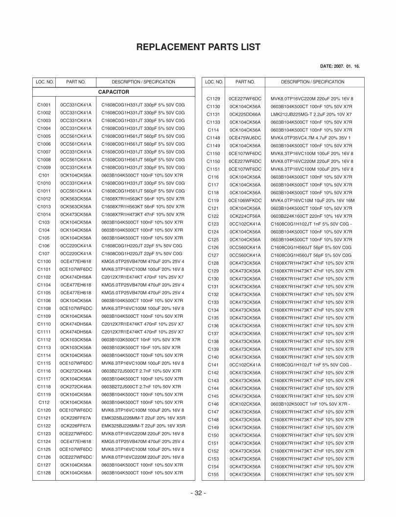
LOC. NO. PART NO. DESCRIPTION / SPECIFICATION
C1001
C1002
C1003
C1004
C1005
C1006
C1007
C1008
C1009
C101
C1010
C1011
C1012
C1013
C1014
C103
C104
C105
C106
C107
C1100
C1101
C1102
C1104
C1105
C1106
C1108
C1109
C1110
C1111
C1112
C1113
C1114
C1115
C1116
C1117
C1118
C1119
C112
C1120
C1121
C1122
C1123
C1124
C1125
C1126
C1127
C1128
0CC331CK41A
0CC331CK41A
0CC331CK41A
0CC331CK41A
0CC561CK41A
0CC561CK41A
0CC331CK41A
0CC561CK41A
0CC331CK41A
0CK104CK56A
0CC331CK41A
0CC561CK41A
0CK563CK56A
0CK563CK56A
0CK473CK56A
0CK104CK56A
0CK104CK56A
0CK104CK56A
0CC220CK41A
0CC220CK41A
0CE477EH618
0CE107WF6DC
0CK474DH56A
0CE477EH618
0CE477EH618
0CK104CK56A
0CE107WF6DC
0CK104CK56A
0CK474DH56A
0CK474DH56A
0CK103CK56A
0CK103CK56A
0CK104CK56A
0CE107WF6DC
0CK272CK46A
0CK104CK56A
0CK272CK46A
0CK104CK56A
0CK104CK56A
0CE107WF6DC
0CK226FF67A
0CK226FF67A
0CE227WF6DC
0CE477EH618
0CE107WF6DC
0CE227WF6DC
0CK104CK56A
0CK104CK56A
C1608C0G1H331JT 330pF 5% 50V C0G
C1608C0G1H331JT 330pF 5% 50V C0G
C1608C0G1H331JT 330pF 5% 50V C0G
C1608C0G1H331JT 330pF 5% 50V C0G
C1608C0G1H561JT 560pF 5% 50V C0G
C1608C0G1H561JT 560pF 5% 50V C0G
C1608C0G1H331JT 330pF 5% 50V C0G
C1608C0G1H561JT 560pF 5% 50V C0G
C1608C0G1H331JT 330pF 5% 50V C0G
0603B104K500CT 100nF 10% 50V X7R
C1608C0G1H331JT 330pF 5% 50V C0G
C1608C0G1H561JT 560pF 5% 50V C0G
C1608X7R1H563KT 56nF 10% 50V X7R
C1608X7R1H563KT 56nF 10% 50V X7R
C1608X7R1H473KT 47nF 10% 50V X7R
0603B104K500CT 100nF 10% 50V X7R
0603B104K500CT 100nF 10% 50V X7R
0603B104K500CT 100nF 10% 50V X7R
C1608C0G1H220JT 22pF 5% 50V C0G
C1608C0G1H220JT 22pF 5% 50V C0G
KMG5.0TP25VB470M 470uF 20% 25V 4
MVK6.3TP16VC100M 100uF 20% 16V 8
C2012X7R1E474KT 470nF 10% 25V X7
KMG5.0TP25VB470M 470uF 20% 25V 4
KMG5.0TP25VB470M 470uF 20% 25V 4
0603B104K500CT 100nF 10% 50V X7R
MVK6.3TP16VC100M 100uF 20% 16V 8
0603B104K500CT 100nF 10% 50V X7R
C2012X7R1E474KT 470nF 10% 25V X7
C2012X7R1E474KT 470nF 10% 25V X7
0603B103K500CT 10nF 10% 50V X7R
0603B103K500CT 10nF 10% 50V X7R
0603B104K500CT 100nF 10% 50V X7R
MVK6.3TP16VC100M 100uF 20% 16V 8
0603B272J500CT 2.7nF 10% 50V X7R
0603B104K500CT 100nF 10% 50V X7R
0603B272J500CT 2.7nF 10% 50V X7R
0603B104K500CT 100nF 10% 50V X7R
0603B104K500CT 100nF 10% 50V X7R
MVK6.3TP16VC100M 100uF 20% 16V 8
EMK325BJ226MM-T 22uF 20% 16V X5R
EMK325BJ226MM-T 22uF 20% 16V X5R
MVK8.0TP16VC220M 220uF 20% 16V 8
KMG5.0TP25VB470M 470uF 20% 25V 4
MVK6.3TP16VC100M 100uF 20% 16V 8
MVK8.0TP16VC220M 220uF 20% 16V 8
0603B104K500CT 100nF 10% 50V X7R
0603B104K500CT 100nF 10% 50V X7R
C1129
C1130
C1131
C1133
C114
C1148
C1149
C1150
C1150
C1151
C116
C117
C118
C119
C121
C122
C123
C124
C125
C126
C127
C128
C129
C130
C131
C132
C133
C134
C135
C136
C137
C138
C139
C140
C141
C142
C143
C144
C145
C146
C147
C148
C149
C150
C151
C152
C153
C154
C155
0CE227WF6DC
0CK104CK56A
0CK225DD66A
0CK104CK56A
0CK104CK56A
0CE475WJ6DC
0CK104CK56A
0CE107WF6DC
0CE227WF6DC
0CE107WF6DC
0CK104CK56A
0CK104CK56A
0CK104CK56A
0CE106WFKDC
0CK104CK56A
0CK224CF56A
0CC102CK41A
0CK104CK56A
0CK104CK56A
0CC560CK41A
0CC560CK41A
0CK473CK56A
0CK473CK56A
0CK473CK56A
0CK473CK56A
0CK473CK56A
0CK473CK56A
0CK473CK56A
0CK473CK56A
0CK473CK56A
0CK473CK56A
0CK473CK56A
0CK473CK56A
0CK473CK56A
0CC102CK41A
0CK473CK56A
0CK473CK56A
0CK473CK56A
0CK473CK56A
0CK102CK56A
0CK473CK56A
0CK473CK56A
0CK473CK56A
0CK473CK56A
0CK473CK56A
0CK473CK56A
0CK473CK56A
0CK473CK56A
0CK473CK56A
MVK8.0TP16VC220M 220uF 20% 16V 8
0603B104K500CT 100nF 10% 50V X7R
LMK212JB225MG-T 2.2uF 20% 10V X7
0603B104K500CT 100nF 10% 50V X7R
0603B104K500CT 100nF 10% 50V X7R
MVK4.0TP35VC4.7M 4.7uF 20% 35V 1
0603B104K500CT 100nF 10% 50V X7R
MVK6.3TP16VC100M 100uF 20% 16V 8
MVK8.0TP16VC220M 220uF 20% 16V 8
MVK6.3TP16VC100M 100uF 20% 16V 8
0603B104K500CT 100nF 10% 50V X7R
0603B104K500CT 100nF 10% 50V X7R
0603B104K500CT 100nF 10% 50V X7R
MVK4.0TP16VC10M 10uF 20% 16V 16M
0603B104K500CT 100nF 10% 50V X7R
0603B224K160CT 220nF 10% 16V X7R
C1608C0G1H102JT 1nF 5% 50V C0G -
0603B104K500CT 100nF 10% 50V X7R
0603B104K500CT 100nF 10% 50V X7R
C1608C0G1H560JT 56pF 5% 50V C0G
C1608C0G1H560JT 56pF 5% 50V C0G
C1608X7R1H473KT 47nF 10% 50V X7R
C1608X7R1H473KT 47nF 10% 50V X7R
C1608X7R1H473KT 47nF 10% 50V X7R
C1608X7R1H473KT 47nF 10% 50V X7R
C1608X7R1H473KT 47nF 10% 50V X7R
C1608X7R1H473KT 47nF 10% 50V X7R
C1608X7R1H473KT 47nF 10% 50V X7R
C1608X7R1H473KT 47nF 10% 50V X7R
C1608X7R1H473KT 47nF 10% 50V X7R
C1608X7R1H473KT 47nF 10% 50V X7R
C1608X7R1H473KT 47nF 10% 50V X7R
C1608X7R1H473KT 47nF 10% 50V X7R
C1608X7R1H473KT 47nF 10% 50V X7R
C1608C0G1H102JT 1nF 5% 50V C0G -
C1608X7R1H473KT 47nF 10% 50V X7R
C1608X7R1H473KT 47nF 10% 50V X7R
C1608X7R1H473KT 47nF 10% 50V X7R
C1608X7R1H473KT 47nF 10% 50V X7R
0603B102K500CT 1nF 10% 50V X7R -
C1608X7R1H473KT 47nF 10% 50V X7R
C1608X7R1H473KT 47nF 10% 50V X7R
C1608X7R1H473KT 47nF 10% 50V X7R
C1608X7R1H473KT 47nF 10% 50V X7R
C1608X7R1H473KT 47nF 10% 50V X7R
C1608X7R1H473KT 47nF 10% 50V X7R
C1608X7R1H473KT 47nF 10% 50V X7R
C1608X7R1H473KT 47nF 10% 50V X7R
C1608X7R1H473KT 47nF 10% 50V X7R
LOC. NO. PART NO. DESCRIPTION / SPECIFICATION
- 32 -
REPLACEMENT PARTS LIST
DATE: 2007. 01. 16.
CAPACITOR
LOC. NO. PART NO. DESCRIPTION / SPECIFICATION
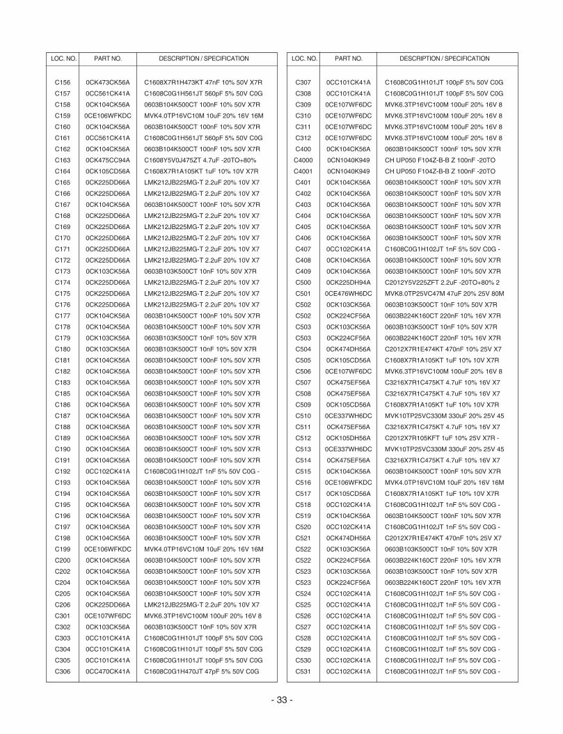
C156
C157
C158
C159
C160
C161
C162
C163
C164
C165
C166
C167
C168
C169
C170
C171
C172
C173
C174
C175
C176
C177
C178
C179
C180
C181
C182
C183
C185
C186
C187
C188
C189
C190
C191
C192
C193
C194
C195
C196
C197
C198
C199
C200
C202
C204
C205
C206
C301
C302
C303
C304
C305
C306
0CK473CK56A
0CC561CK41A
0CK104CK56A
0CE106WFKDC
0CK104CK56A
0CC561CK41A
0CK104CK56A
0CK475CC94A
0CK105CD56A
0CK225DD66A
0CK225DD66A
0CK104CK56A
0CK225DD66A
0CK225DD66A
0CK225DD66A
0CK225DD66A
0CK225DD66A
0CK103CK56A
0CK225DD66A
0CK225DD66A
0CK225DD66A
0CK104CK56A
0CK104CK56A
0CK103CK56A
0CK103CK56A
0CK104CK56A
0CK104CK56A
0CK104CK56A
0CK104CK56A
0CK104CK56A
0CK104CK56A
0CK104CK56A
0CK104CK56A
0CK104CK56A
0CK104CK56A
0CC102CK41A
0CK104CK56A
0CK104CK56A
0CK104CK56A
0CK104CK56A
0CK104CK56A
0CK104CK56A
0CE106WFKDC
0CK104CK56A
0CK104CK56A
0CK104CK56A
0CK104CK56A
0CK225DD66A
0CE107WF6DC
0CK103CK56A
0CC101CK41A
0CC101CK41A
0CC101CK41A
0CC470CK41A
C1608X7R1H473KT 47nF 10% 50V X7R
C1608C0G1H561JT 560pF 5% 50V C0G
0603B104K500CT 100nF 10% 50V X7R
MVK4.0TP16VC10M 10uF 20% 16V 16M
0603B104K500CT 100nF 10% 50V X7R
C1608C0G1H561JT 560pF 5% 50V C0G
0603B104K500CT 100nF 10% 50V X7R
C1608Y5V0J475ZT 4.7uF -20TO+80%
C1608X7R1A105KT 1uF 10% 10V X7R
LMK212JB225MG-T 2.2uF 20% 10V X7
LMK212JB225MG-T 2.2uF 20% 10V X7
0603B104K500CT 100nF 10% 50V X7R
LMK212JB225MG-T 2.2uF 20% 10V X7
LMK212JB225MG-T 2.2uF 20% 10V X7
LMK212JB225MG-T 2.2uF 20% 10V X7
LMK212JB225MG-T 2.2uF 20% 10V X7
LMK212JB225MG-T 2.2uF 20% 10V X7
0603B103K500CT 10nF 10% 50V X7R
LMK212JB225MG-T 2.2uF 20% 10V X7
LMK212JB225MG-T 2.2uF 20% 10V X7
LMK212JB225MG-T 2.2uF 20% 10V X7
0603B104K500CT 100nF 10% 50V X7R
0603B104K500CT 100nF 10% 50V X7R
0603B103K500CT 10nF 10% 50V X7R
0603B103K500CT 10nF 10% 50V X7R
0603B104K500CT 100nF 10% 50V X7R
0603B104K500CT 100nF 10% 50V X7R
0603B104K500CT 100nF 10% 50V X7R
0603B104K500CT 100nF 10% 50V X7R
0603B104K500CT 100nF 10% 50V X7R
0603B104K500CT 100nF 10% 50V X7R
0603B104K500CT 100nF 10% 50V X7R
0603B104K500CT 100nF 10% 50V X7R
0603B104K500CT 100nF 10% 50V X7R
0603B104K500CT 100nF 10% 50V X7R
C1608C0G1H102JT 1nF 5% 50V C0G -
0603B104K500CT 100nF 10% 50V X7R
0603B104K500CT 100nF 10% 50V X7R
0603B104K500CT 100nF 10% 50V X7R
0603B104K500CT 100nF 10% 50V X7R
0603B104K500CT 100nF 10% 50V X7R
0603B104K500CT 100nF 10% 50V X7R
MVK4.0TP16VC10M 10uF 20% 16V 16M
0603B104K500CT 100nF 10% 50V X7R
0603B104K500CT 100nF 10% 50V X7R
0603B104K500CT 100nF 10% 50V X7R
0603B104K500CT 100nF 10% 50V X7R
LMK212JB225MG-T 2.2uF 20% 10V X7
MVK6.3TP16VC100M 100uF 20% 16V 8
0603B103K500CT 10nF 10% 50V X7R
C1608C0G1H101JT 100pF 5% 50V C0G
C1608C0G1H101JT 100pF 5% 50V C0G
C1608C0G1H101JT 100pF 5% 50V C0G
C1608C0G1H470JT 47pF 5% 50V C0G
C307
C308
C309
C310
C311
C312
C400
C4000
C4001
C401
C402
C403
C404
C405
C406
C407
C408
C409
C500
C501
C502
C502
C503
C503
C504
C505
C506
C507
C508
C509
C510
C511
C512
C513
C514
C515
C516
C517
C518
C519
C520
C521
C522
C522
C523
C523
C524
C525
C526
C527
C528
C529
C530
C531
0CC101CK41A
0CC101CK41A
0CE107WF6DC
0CE107WF6DC
0CE107WF6DC
0CE107WF6DC
0CK104CK56A
0CN1040K949
0CN1040K949
0CK104CK56A
0CK104CK56A
0CK104CK56A
0CK104CK56A
0CK104CK56A
0CK104CK56A
0CC102CK41A
0CK104CK56A
0CK104CK56A
0CK225DH94A
0CE476WH6DC
0CK103CK56A
0CK224CF56A
0CK103CK56A
0CK224CF56A
0CK474DH56A
0CK105CD56A
0CE107WF6DC
0CK475EF56A
0CK475EF56A
0CK105CD56A
0CE337WH6DC
0CK475EF56A
0CK105DH56A
0CE337WH6DC
0CK475EF56A
0CK104CK56A
0CE106WFKDC
0CK105CD56A
0CC102CK41A
0CK104CK56A
0CC102CK41A
0CK474DH56A
0CK103CK56A
0CK224CF56A
0CK103CK56A
0CK224CF56A
0CC102CK41A
0CC102CK41A
0CC102CK41A
0CC102CK41A
0CC102CK41A
0CC102CK41A
0CC102CK41A
0CC102CK41A
C1608C0G1H101JT 100pF 5% 50V C0G
C1608C0G1H101JT 100pF 5% 50V C0G
MVK6.3TP16VC100M 100uF 20% 16V 8
MVK6.3TP16VC100M 100uF 20% 16V 8
MVK6.3TP16VC100M 100uF 20% 16V 8
MVK6.3TP16VC100M 100uF 20% 16V 8
0603B104K500CT 100nF 10% 50V X7R
CH UP050 F104Z-B-B Z 100nF -20TO
CH UP050 F104Z-B-B Z 100nF -20TO
0603B104K500CT 100nF 10% 50V X7R
0603B104K500CT 100nF 10% 50V X7R
0603B104K500CT 100nF 10% 50V X7R
0603B104K500CT 100nF 10% 50V X7R
0603B104K500CT 100nF 10% 50V X7R
0603B104K500CT 100nF 10% 50V X7R
C1608C0G1H102JT 1nF 5% 50V C0G -
0603B104K500CT 100nF 10% 50V X7R
0603B104K500CT 100nF 10% 50V X7R
C2012Y5V225ZFT 2.2uF -20TO+80% 2
MVK8.0TP25VC47M 47uF 20% 25V 80M
0603B103K500CT 10nF 10% 50V X7R
0603B224K160CT 220nF 10% 16V X7R
0603B103K500CT 10nF 10% 50V X7R
0603B224K160CT 220nF 10% 16V X7R
C2012X7R1E474KT 470nF 10% 25V X7
C1608X7R1A105KT 1uF 10% 10V X7R
MVK6.3TP16VC100M 100uF 20% 16V 8
C3216X7R1C475KT 4.7uF 10% 16V X7
C3216X7R1C475KT 4.7uF 10% 16V X7
C1608X7R1A105KT 1uF 10% 10V X7R
MVK10TP25VC330M 330uF 20% 25V 45
C3216X7R1C475KT 4.7uF 10% 16V X7
C2012X7R105KFT 1uF 10% 25V X7R -
MVK10TP25VC330M 330uF 20% 25V 45
C3216X7R1C475KT 4.7uF 10% 16V X7
0603B104K500CT 100nF 10% 50V X7R
MVK4.0TP16VC10M 10uF 20% 16V 16M
C1608X7R1A105KT 1uF 10% 10V X7R
C1608C0G1H102JT 1nF 5% 50V C0G -
0603B104K500CT 100nF 10% 50V X7R
C1608C0G1H102JT 1nF 5% 50V C0G -
C2012X7R1E474KT 470nF 10% 25V X7
0603B103K500CT 10nF 10% 50V X7R
0603B224K160CT 220nF 10% 16V X7R
0603B103K500CT 10nF 10% 50V X7R
0603B224K160CT 220nF 10% 16V X7R
C1608C0G1H102JT 1nF 5% 50V C0G -
C1608C0G1H102JT 1nF 5% 50V C0G -
C1608C0G1H102JT 1nF 5% 50V C0G -
C1608C0G1H102JT 1nF 5% 50V C0G -
C1608C0G1H102JT 1nF 5% 50V C0G -
C1608C0G1H102JT 1nF 5% 50V C0G -
C1608C0G1H102JT 1nF 5% 50V C0G -
C1608C0G1H102JT 1nF 5% 50V C0G -
LOC. NO. PART NO. DESCRIPTION / SPECIFICATION
- 33 -
LOC. NO. PART NO. DESCRIPTION / SPECIFICATION
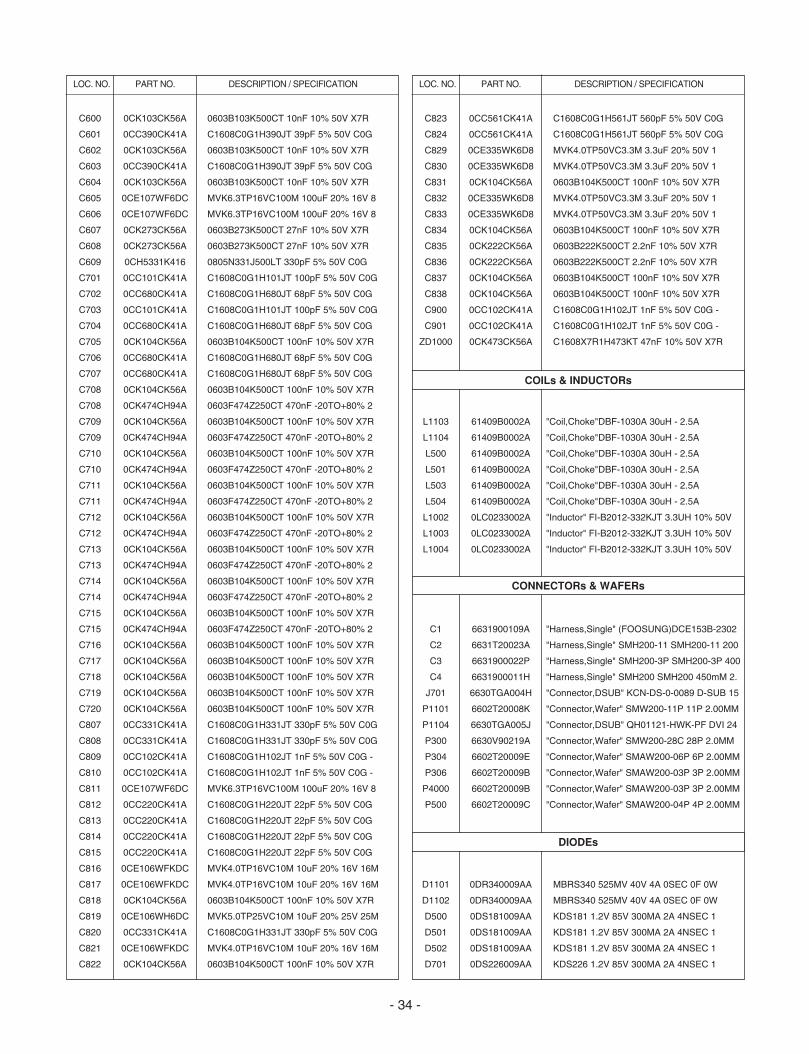
C600
C601
C602
C603
C604
C605
C606
C607
C608
C609
C701
C702
C703
C704
C705
C706
C707
C708
C708
C709
C709
C710
C710
C711
C711
C712
C712
C713
C713
C714
C714
C715
C715
C716
C717
C718
C719
C720
C807
C808
C809
C810
C811
C812
C813
C814
C815
C816
C817
C818
C819
C820
C821
C822
0CK103CK56A
0CC390CK41A
0CK103CK56A
0CC390CK41A
0CK103CK56A
0CE107WF6DC
0CE107WF6DC
0CK273CK56A
0CK273CK56A
0CH5331K416
0CC101CK41A
0CC680CK41A
0CC101CK41A
0CC680CK41A
0CK104CK56A
0CC680CK41A
0CC680CK41A
0CK104CK56A
0CK474CH94A
0CK104CK56A
0CK474CH94A
0CK104CK56A
0CK474CH94A
0CK104CK56A
0CK474CH94A
0CK104CK56A
0CK474CH94A
0CK104CK56A
0CK474CH94A
0CK104CK56A
0CK474CH94A
0CK104CK56A
0CK474CH94A
0CK104CK56A
0CK104CK56A
0CK104CK56A
0CK104CK56A
0CK104CK56A
0CC331CK41A
0CC331CK41A
0CC102CK41A
0CC102CK41A
0CE107WF6DC
0CC220CK41A
0CC220CK41A
0CC220CK41A
0CC220CK41A
0CE106WFKDC
0CE106WFKDC
0CK104CK56A
0CE106WH6DC
0CC331CK41A
0CE106WFKDC
0CK104CK56A
0603B103K500CT 10nF 10% 50V X7R
C1608C0G1H390JT 39pF 5% 50V C0G
0603B103K500CT 10nF 10% 50V X7R
C1608C0G1H390JT 39pF 5% 50V C0G
0603B103K500CT 10nF 10% 50V X7R
MVK6.3TP16VC100M 100uF 20% 16V 8
MVK6.3TP16VC100M 100uF 20% 16V 8
0603B273K500CT 27nF 10% 50V X7R
0603B273K500CT 27nF 10% 50V X7R
0805N331J500LT 330pF 5% 50V C0G
C1608C0G1H101JT 100pF 5% 50V C0G
C1608C0G1H680JT 68pF 5% 50V C0G
C1608C0G1H101JT 100pF 5% 50V C0G
C1608C0G1H680JT 68pF 5% 50V C0G
0603B104K500CT 100nF 10% 50V X7R
C1608C0G1H680JT 68pF 5% 50V C0G
C1608C0G1H680JT 68pF 5% 50V C0G
0603B104K500CT 100nF 10% 50V X7R
0603F474Z250CT 470nF -20TO+80% 2
0603B104K500CT 100nF 10% 50V X7R
0603F474Z250CT 470nF -20TO+80% 2
0603B104K500CT 100nF 10% 50V X7R
0603F474Z250CT 470nF -20TO+80% 2
0603B104K500CT 100nF 10% 50V X7R
0603F474Z250CT 470nF -20TO+80% 2
0603B104K500CT 100nF 10% 50V X7R
0603F474Z250CT 470nF -20TO+80% 2
0603B104K500CT 100nF 10% 50V X7R
0603F474Z250CT 470nF -20TO+80% 2
0603B104K500CT 100nF 10% 50V X7R
0603F474Z250CT 470nF -20TO+80% 2
0603B104K500CT 100nF 10% 50V X7R
0603F474Z250CT 470nF -20TO+80% 2
0603B104K500CT 100nF 10% 50V X7R
0603B104K500CT 100nF 10% 50V X7R
0603B104K500CT 100nF 10% 50V X7R
0603B104K500CT 100nF 10% 50V X7R
0603B104K500CT 100nF 10% 50V X7R
C1608C0G1H331JT 330pF 5% 50V C0G
C1608C0G1H331JT 330pF 5% 50V C0G
C1608C0G1H102JT 1nF 5% 50V C0G -
C1608C0G1H102JT 1nF 5% 50V C0G -
MVK6.3TP16VC100M 100uF 20% 16V 8
C1608C0G1H220JT 22pF 5% 50V C0G
C1608C0G1H220JT 22pF 5% 50V C0G
C1608C0G1H220JT 22pF 5% 50V C0G
C1608C0G1H220JT 22pF 5% 50V C0G
MVK4.0TP16VC10M 10uF 20% 16V 16M
MVK4.0TP16VC10M 10uF 20% 16V 16M
0603B104K500CT 100nF 10% 50V X7R
MVK5.0TP25VC10M 10uF 20% 25V 25M
C1608C0G1H331JT 330pF 5% 50V C0G
MVK4.0TP16VC10M 10uF 20% 16V 16M
0603B104K500CT 100nF 10% 50V X7R
C823
C824
C829
C830
C831
C832
C833
C834
C835
C836
C837
C838
C900
C901
ZD1000
L1103
L1104
L500
L501
L503
L504
L1002
L1003
L1004
C1
C2
C3
C4
J701
P1101
P1104
P300
P304
P306
P4000
P500
D1101
D1102
D500
D501
D502
D701
0CC561CK41A
0CC561CK41A
0CE335WK6D8
0CE335WK6D8
0CK104CK56A
0CE335WK6D8
0CE335WK6D8
0CK104CK56A
0CK222CK56A
0CK222CK56A
0CK104CK56A
0CK104CK56A
0CC102CK41A
0CC102CK41A
0CK473CK56A
61409B0002A
61409B0002A
61409B0002A
61409B0002A
61409B0002A
61409B0002A
0LC0233002A
0LC0233002A
0LC0233002A
6631900109A
6631T20023A
6631900022P
6631900011H
6630TGA004H
6602T20008K
6630TGA005J
6630V90219A
6602T20009E
6602T20009B
6602T20009B
6602T20009C
0DR340009AA
0DR340009AA
0DS181009AA
0DS181009AA
0DS181009AA
0DS226009AA
C1608C0G1H561JT 560pF 5% 50V C0G
C1608C0G1H561JT 560pF 5% 50V C0G
MVK4.0TP50VC3.3M 3.3uF 20% 50V 1
MVK4.0TP50VC3.3M 3.3uF 20% 50V 1
0603B104K500CT 100nF 10% 50V X7R
MVK4.0TP50VC3.3M 3.3uF 20% 50V 1
MVK4.0TP50VC3.3M 3.3uF 20% 50V 1
0603B104K500CT 100nF 10% 50V X7R
0603B222K500CT 2.2nF 10% 50V X7R
0603B222K500CT 2.2nF 10% 50V X7R
0603B104K500CT 100nF 10% 50V X7R
0603B104K500CT 100nF 10% 50V X7R
C1608C0G1H102JT 1nF 5% 50V C0G -
C1608C0G1H102JT 1nF 5% 50V C0G -
C1608X7R1H473KT 47nF 10% 50V X7R
"Coil,Choke"DBF-1030A 30uH - 2.5A
"Coil,Choke"DBF-1030A 30uH - 2.5A
"Coil,Choke"DBF-1030A 30uH - 2.5A
"Coil,Choke"DBF-1030A 30uH - 2.5A
"Coil,Choke"DBF-1030A 30uH - 2.5A
"Coil,Choke"DBF-1030A 30uH - 2.5A
"Inductor" FI-B2012-332KJT 3.3UH 10% 50V
"Inductor" FI-B2012-332KJT 3.3UH 10% 50V
"Inductor" FI-B2012-332KJT 3.3UH 10% 50V
"Harness,Single" (FOOSUNG)DCE153B-2302
"Harness,Single" SMH200-11 SMH200-11 200
"Harness,Single" SMH200-3P SMH200-3P 400
"Harness,Single" SMH200 SMH200 450mM 2.
"Connector,DSUB" KCN-DS-0-0089 D-SUB 15
"Connector,Wafer" SMW200-11P 11P 2.00MM
"Connector,DSUB" QH01121-HWK-PF DVI 24
"Connector,Wafer" SMW200-28C 28P 2.0MM
"Connector,Wafer" SMAW200-06P 6P 2.00MM
"Connector,Wafer" SMAW200-03P 3P 2.00MM
"Connector,Wafer" SMAW200-03P 3P 2.00MM
"Connector,Wafer" SMAW200-04P 4P 2.00MM
MBRS340 525MV 40V 4A 0SEC 0F 0W
MBRS340 525MV 40V 4A 0SEC 0F 0W
KDS181 1.2V 85V 300MA 2A 4NSEC 1
KDS181 1.2V 85V 300MA 2A 4NSEC 1
KDS181 1.2V 85V 300MA 2A 4NSEC 1
KDS226 1.2V 85V 300MA 2A 4NSEC 1
LOC. NO. PART NO. DESCRIPTION / SPECIFICATION
- 34 -
COILs & INDUCTORs
CONNECTORs & WAFERs
DIODEs
LOC. NO. PART NO. DESCRIPTION / SPECIFICATION
D702
D703
D704
D705
D706
D707
D708
D709
D710
D711
D712
D713
D714
D715
ZD1000
ZD1005
ZD1006
ZD1007
ZD1008
ZD1009
ZD1010
ZD1011
ZD1013
ZD1014
ZD1015
ZD1016
ZD1017
ZD1018
ZD1019
ZD1020
ZD1021
ZD1034
ZD2001
ZD4000
ZD4001
ZD701
ZD702
ZD703
ZD704
ZD705
ZD708
ZD709
ZD710
ZD801
ZD802
ZD803
ZD804
ZD805
ZD806
ZD807
ZD808
ZD809
ZD810
ZD811
0DS226009AA
0DS226009AA
0DS226009AA
0DS226009AA
0DS226009AA
0DS226009AA
0DS226009AA
0DS226009AA
0DS226009AA
0DS226009AA
0DSON00138A
0DSON00138A
0DD184009AA
0DD184009AA
0DZ560009GB
0DZ560009GB
0DZ560009GB
0DZ560009GB
0DZ560009GB
0DZ560009GB
0DZ560009GB
0DZ560009GB
0DZ560009GB
0DZ560009GB
0DZ560009GB
0DZ560009GB
0DZ560009GB
0DZ560009GB
0DZ560009GB
0DZ560009GB
0DZ560009GB
0DZ560009GB
0DZ560009AA
0DZ560009CF
0DZ560009CF
0DZ560009GB
0DZ560009GB
0DZ560009GB
0DZ560009GB
0DZ560009GB
0DZ560009GB
0DZ560009GB
0DZ560009GB
0DZ560009GB
0DZ560009GB
0DZ560009GB
0DZ560009GB
0DZ560009GB
0DZ560009GB
0DZ560009GB
0DZ560009GB
0DZ560009GB
0DZ560009GB
0DZ560009GB
KDS226 1.2V 85V 300MA 2A 4NSEC 1
KDS226 1.2V 85V 300MA 2A 4NSEC 1
KDS226 1.2V 85V 300MA 2A 4NSEC 1
KDS226 1.2V 85V 300MA 2A 4NSEC 1
KDS226 1.2V 85V 300MA 2A 4NSEC 1
KDS226 1.2V 85V 300MA 2A 4NSEC 1
KDS226 1.2V 85V 300MA 2A 4NSEC 1
KDS226 1.2V 85V 300MA 2A 4NSEC 1
KDS226 1.2V 85V 300MA 2A 4NSEC 1
KDS226 1.2V 85V 300MA 2A 4NSEC 1
MMBD301LT1G 600MV 30V - - 1.5pF
MMBD301LT1G 600MV 30V - - 1.5pF
KDS184 KDS184 TP KEC - 85V - - -
KDS184 KDS184 TP KEC - 85V - - -
BZT52C5V6S-(F) 5.6V 5.2TO6V 40OH
BZT52C5V6S-(F) 5.6V 5.2TO6V 40OH
BZT52C5V6S-(F) 5.6V 5.2TO6V 40OH
BZT52C5V6S-(F) 5.6V 5.2TO6V 40OH
BZT52C5V6S-(F) 5.6V 5.2TO6V 40OH
BZT52C5V6S-(F) 5.6V 5.2TO6V 40OH
BZT52C5V6S-(F) 5.6V 5.2TO6V 40OH
BZT52C5V6S-(F) 5.6V 5.2TO6V 40OH
BZT52C5V6S-(F) 5.6V 5.2TO6V 40OH
BZT52C5V6S-(F) 5.6V 5.2TO6V 40OH
BZT52C5V6S-(F) 5.6V 5.2TO6V 40OH
BZT52C5V6S-(F) 5.6V 5.2TO6V 40OH
BZT52C5V6S-(F) 5.6V 5.2TO6V 40OH
BZT52C5V6S-(F) 5.6V 5.2TO6V 40OH
BZT52C5V6S-(F) 5.6V 5.2TO6V 40OH
BZT52C5V6S-(F) 5.6V 5.2TO6V 40OH
BZT52C5V6S-(F) 5.6V 5.2TO6V 40OH
BZT52C5V6S-(F) 5.6V 5.2TO6V 40OH
MTZJ5.6B 5.6V 5.45TO5.73V 40OHM
MTZJ5.6B 5.6V 5.45TO5.73V 40OHM
MTZJ5.6B 5.6V 5.45TO5.73V 40OHM
BZT52C5V6S-(F) 5.6V 5.2TO6V 40OH
BZT52C5V6S-(F) 5.6V 5.2TO6V 40OH
BZT52C5V6S-(F) 5.6V 5.2TO6V 40OH
BZT52C5V6S-(F) 5.6V 5.2TO6V 40OH
BZT52C5V6S-(F) 5.6V 5.2TO6V 40OH
BZT52C5V6S-(F) 5.6V 5.2TO6V 40OH
BZT52C5V6S-(F) 5.6V 5.2TO6V 40OH
BZT52C5V6S-(F) 5.6V 5.2TO6V 40OH
BZT52C5V6S-(F) 5.6V 5.2TO6V 40OH
BZT52C5V6S-(F) 5.6V 5.2TO6V 40OH
BZT52C5V6S-(F) 5.6V 5.2TO6V 40OH
BZT52C5V6S-(F) 5.6V 5.2TO6V 40OH
BZT52C5V6S-(F) 5.6V 5.2TO6V 40OH
BZT52C5V6S-(F) 5.6V 5.2TO6V 40OH
BZT52C5V6S-(F) 5.6V 5.2TO6V 40OH
BZT52C5V6S-(F) 5.6V 5.2TO6V 40OH
BZT52C5V6S-(F) 5.6V 5.2TO6V 40OH
BZT52C5V6S-(F) 5.6V 5.2TO6V 40OH
BZT52C5V6S-(F) 5.6V 5.2TO6V 40OH
ZD812
ZD813
ZD814
ZD815
ZD900
ZD901
ZD902
ZD903
ZD904
ZD905
ZD906
ZD907
L1000
L1001
L1006
L1007
L1113
L1114
L1115
L1116
L1117
L505
L506
L507
L508
L509
L510
L511
L512
L801
L802
L803
L804
L805
L806
L807
L808
L900
L901
IC100
IC102
IC103
IC1100
IC1101
IC1102
IC1103
IC1104
IC1105
0DZ560009GB
0DZ560009GB
0DZ560009GB
0DZ560009GB
0DZ560009GB
0DZ560009GB
0DZ560009GB
0DZ560009GB
0DZ560009GB
0DZ560009GB
0DZ560009GB
0DZ560009GB
6210TCE001A
6210TCE001A
6210TCE001A
6210TCE001A
6210TCE001G
6200J00005E
6210TCE001G
6200J00005E
6200J00005E
6210TCE001G
6210TCE001G
6210TCE001G
6210TCE001G
6210TCE001G
6210TCE001G
6210TCE001G
6210TCE001G
6210TCE001A
6210TCE001A
6210TCE001A
6210TCE001A
6200J00005E
6200J00005E
6200J00005E
6210TCE001A
6210TCE001A
6210TCE001A
EAN33715804
EAN35392002
0IMMRAL026C
0IPRPSG025A
0IPMGSG016A
0IMCRMZ001A
0IMCRMZ001A
0IPMG00107A
0IMCRRH001A
BZT52C5V6S-(F) 5.6V 5.2TO6V 40OH
BZT52C5V6S-(F) 5.6V 5.2TO6V 40OH
BZT52C5V6S-(F) 5.6V 5.2TO6V 40OH
BZT52C5V6S-(F) 5.6V 5.2TO6V 40OH
BZT52C5V6S-(F) 5.6V 5.2TO6V 40OH
BZT52C5V6S-(F) 5.6V 5.2TO6V 40OH
BZT52C5V6S-(F) 5.6V 5.2TO6V 40OH
BZT52C5V6S-(F) 5.6V 5.2TO6V 40OH
BZT52C5V6S-(F) 5.6V 5.2TO6V 40OH
BZT52C5V6S-(F) 5.6V 5.2TO6V 40OH
BZT52C5V6S-(F) 5.6V 5.2TO6V 40OH
BZT52C5V6S-(F) 5.6V 5.2TO6V 40OH
HB-1S2012-080JT 8OHM 2X1.25X1MM
HB-1S2012-080JT 8OHM 2X1.25X1MM
HB-1S2012-080JT 8OHM 2X1.25X1MM
HB-1S2012-080JT 8OHM 2X1.25X1MM
HH-1M3216-501JT 500OHM 3.2X1.6X1
HH-1M2012-601JT 600OHM 2X1.25X1M
HH-1M3216-501JT 500OHM 3.2X1.6X1
HH-1M2012-601JT 600OHM 2X1.25X1M
HH-1M2012-601JT 600OHM 2X1.25X1M
HH-1M3216-501JT 500OHM 3.2X1.6X1
HH-1M3216-501JT 500OHM 3.2X1.6X1
HH-1M3216-501JT 500OHM 3.2X1.6X1
HH-1M3216-501JT 500OHM 3.2X1.6X1
HH-1M3216-501JT 500OHM 3.2X1.6X1
HH-1M3216-501JT 500OHM 3.2X1.6X1
HH-1M3216-501JT 500OHM 3.2X1.6X1
HH-1M3216-501JT 500OHM 3.2X1.6X1
HB-1S2012-080JT 8OHM 2X1.25X1MM
HB-1S2012-080JT 8OHM 2X1.25X1MM
HB-1S2012-080JT 8OHM 2X1.25X1MM
HB-1S2012-080JT 8OHM 2X1.25X1MM
HH-1M2012-601JT 600OHM 2X1.25X1M
HH-1M2012-601JT 600OHM 2X1.25X1M
HH-1M2012-601JT 600OHM 2X1.25X1M
HB-1S2012-080JT 8OHM 2X1.25X1MM
HB-1S2012-080JT 8OHM 2X1.25X1MM
HB-1S2012-080JT 8OHM 2X1.25X1MM
"LGE9789AD-LF 300MVTO3.6V,300MVTO"
M208WA-BZH Micom Ass'y
AT24C64AN-10SU-2.7 64KBIT 8192x8
LD1086D2M33 4.9TO30V 3.3V - D2PA
LD1086D2T18TR 3.4TO30V 1.8V - D2
"MP1583DN-Z,LF 4.75TO23V 21V 0W S"
"MP1583DN-Z,LF 4.75TO23V 21V 0W S"
AZ1117H-2.5TR/E1 15V 2.5V 0W SOT
BA033FP-E2 4.3TO25V 3.3V 1W TO25
LOC. NO. PART NO. DESCRIPTION / SPECIFICATION
- 35 -
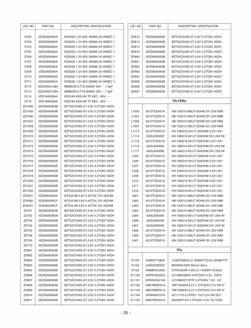
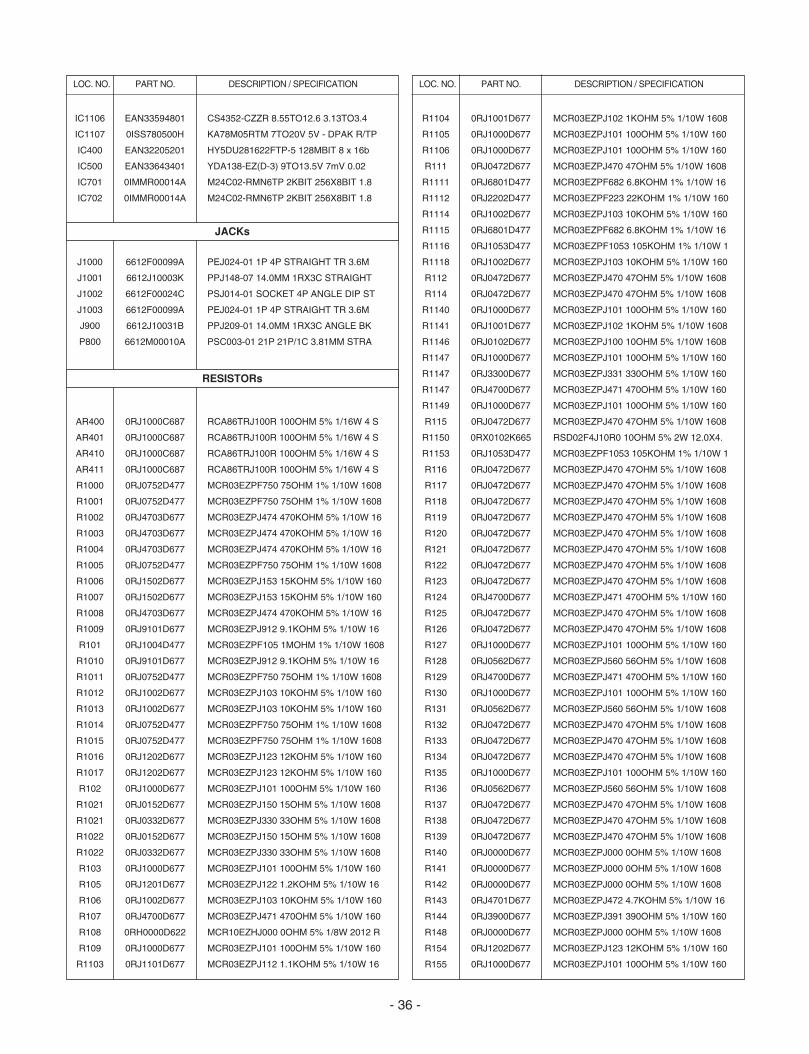
FILTERs
ICs
LOC. NO. PART NO. DESCRIPTION / SPECIFICATION
IC1106
IC1107
IC400
IC500
IC701
IC702
J1000
J1001
J1002
J1003
J900
P800
AR400
AR401
AR410
AR411
R1000
R1001
R1002
R1003
R1004
R1005
R1006
R1007
R1008
R1009
R101
R1010
R1011
R1012
R1013
R1014
R1015
R1016
R1017
R102
R1021
R1021
R1022
R1022
R103
R105
R106
R107
R108
R109
R1103
EAN33594801
0ISS780500H
EAN32205201
EAN33643401
0IMMR00014A
0IMMR00014A
6612F00099A
6612J10003K
6612F00024C
6612F00099A
6612J10031B
6612M00010A
0RJ1000C687
0RJ1000C687
0RJ1000C687
0RJ1000C687
0RJ0752D477
0RJ0752D477
0RJ4703D677
0RJ4703D677
0RJ4703D677
0RJ0752D477
0RJ1502D677
0RJ1502D677
0RJ4703D677
0RJ9101D677
0RJ1004D477
0RJ9101D677
0RJ0752D477
0RJ1002D677
0RJ1002D677
0RJ0752D477
0RJ0752D477
0RJ1202D677
0RJ1202D677
0RJ1000D677
0RJ0152D677
0RJ0332D677
0RJ0152D677
0RJ0332D677
0RJ1000D677
0RJ1201D677
0RJ1002D677
0RJ4700D677
0RH0000D622
0RJ1000D677
0RJ1101D677
CS4352-CZZR 8.55TO12.6 3.13TO3.4
KA78M05RTM 7TO20V 5V - DPAK R/TP
HY5DU281622FTP-5 128MBIT 8 x 16b
YDA138-EZ(D-3) 9TO13.5V 7mV 0.02
M24C02-RMN6TP 2KBIT 256X8BIT 1.8
M24C02-RMN6TP 2KBIT 256X8BIT 1.8
PEJ024-01 1P 4P STRAIGHT TR 3.6M
PPJ148-07 14.0MM 1RX3C STRAIGHT
PSJ014-01 SOCKET 4P ANGLE DIP ST
PEJ024-01 1P 4P STRAIGHT TR 3.6M
PPJ209-01 14.0MM 1RX3C ANGLE BK
PSC003-01 21P 21P/1C 3.81MM STRA
RCA86TRJ100R 100OHM 5% 1/16W 4 S
RCA86TRJ100R 100OHM 5% 1/16W 4 S
RCA86TRJ100R 100OHM 5% 1/16W 4 S
RCA86TRJ100R 100OHM 5% 1/16W 4 S
MCR03EZPF750 75OHM 1% 1/10W 1608
MCR03EZPF750 75OHM 1% 1/10W 1608
MCR03EZPJ474 470KOHM 5% 1/10W 16
MCR03EZPJ474 470KOHM 5% 1/10W 16
MCR03EZPJ474 470KOHM 5% 1/10W 16
MCR03EZPF750 75OHM 1% 1/10W 1608
MCR03EZPJ153 15KOHM 5% 1/10W 160
MCR03EZPJ153 15KOHM 5% 1/10W 160
MCR03EZPJ474 470KOHM 5% 1/10W 16
MCR03EZPJ912 9.1KOHM 5% 1/10W 16
MCR03EZPF105 1MOHM 1% 1/10W 1608
MCR03EZPJ912 9.1KOHM 5% 1/10W 16
MCR03EZPF750 75OHM 1% 1/10W 1608
MCR03EZPJ103 10KOHM 5% 1/10W 160
MCR03EZPJ103 10KOHM 5% 1/10W 160
MCR03EZPF750 75OHM 1% 1/10W 1608
MCR03EZPF750 75OHM 1% 1/10W 1608
MCR03EZPJ123 12KOHM 5% 1/10W 160
MCR03EZPJ123 12KOHM 5% 1/10W 160
MCR03EZPJ101 100OHM 5% 1/10W 160
MCR03EZPJ150 15OHM 5% 1/10W 1608
MCR03EZPJ330 33OHM 5% 1/10W 1608
MCR03EZPJ150 15OHM 5% 1/10W 1608
MCR03EZPJ330 33OHM 5% 1/10W 1608
MCR03EZPJ101 100OHM 5% 1/10W 160
MCR03EZPJ122 1.2KOHM 5% 1/10W 16
MCR03EZPJ103 10KOHM 5% 1/10W 160
MCR03EZPJ471 470OHM 5% 1/10W 160
MCR10EZHJ000 0OHM 5% 1/8W 2012 R
MCR03EZPJ101 100OHM 5% 1/10W 160
MCR03EZPJ112 1.1KOHM 5% 1/10W 16
R1104
R1105
R1106
R111
R1111
R1112
R1114
R1115
R1116
R1118
R112
R114
R1140
R1141
R1146
R1147
R1147
R1147
R1149
R115
R1150
R1153
R116
R117
R118
R119
R120
R121
R122
R123
R124
R125
R126
R127
R128
R129
R130
R131
R132
R133
R134
R135
R136
R137
R138
R139
R140
R141
R142
R143
R144
R148
R154
R155
0RJ1001D677
0RJ1000D677
0RJ1000D677
0RJ0472D677
0RJ6801D477
0RJ2202D477
0RJ1002D677
0RJ6801D477
0RJ1053D477
0RJ1002D677
0RJ0472D677
0RJ0472D677
0RJ1000D677
0RJ1001D677
0RJ0102D677
0RJ1000D677
0RJ3300D677
0RJ4700D677
0RJ1000D677
0RJ0472D677
0RX0102K665
0RJ1053D477
0RJ0472D677
0RJ0472D677
0RJ0472D677
0RJ0472D677
0RJ0472D677
0RJ0472D677
0RJ0472D677
0RJ0472D677
0RJ4700D677
0RJ0472D677
0RJ0472D677
0RJ1000D677
0RJ0562D677
0RJ4700D677
0RJ1000D677
0RJ0562D677
0RJ0472D677
0RJ0472D677
0RJ0472D677
0RJ1000D677
0RJ0562D677
0RJ0472D677
0RJ0472D677
0RJ0472D677
0RJ0000D677
0RJ0000D677
0RJ0000D677
0RJ4701D677
0RJ3900D677
0RJ0000D677
0RJ1202D677
0RJ1000D677
MCR03EZPJ102 1KOHM 5% 1/10W 1608
MCR03EZPJ101 100OHM 5% 1/10W 160
MCR03EZPJ101 100OHM 5% 1/10W 160
MCR03EZPJ470 47OHM 5% 1/10W 1608
MCR03EZPF682 6.8KOHM 1% 1/10W 16
MCR03EZPF223 22KOHM 1% 1/10W 160
MCR03EZPJ103 10KOHM 5% 1/10W 160
MCR03EZPF682 6.8KOHM 1% 1/10W 16
MCR03EZPF1053 105KOHM 1% 1/10W 1
MCR03EZPJ103 10KOHM 5% 1/10W 160
MCR03EZPJ470 47OHM 5% 1/10W 1608
MCR03EZPJ470 47OHM 5% 1/10W 1608
MCR03EZPJ101 100OHM 5% 1/10W 160
MCR03EZPJ102 1KOHM 5% 1/10W 1608
MCR03EZPJ100 10OHM 5% 1/10W 1608
MCR03EZPJ101 100OHM 5% 1/10W 160
MCR03EZPJ331 330OHM 5% 1/10W 160
MCR03EZPJ471 470OHM 5% 1/10W 160
MCR03EZPJ101 100OHM 5% 1/10W 160
MCR03EZPJ470 47OHM 5% 1/10W 1608
RSD02F4J10R0 10OHM 5% 2W 12.0X4.
MCR03EZPF1053 105KOHM 1% 1/10W 1
MCR03EZPJ470 47OHM 5% 1/10W 1608
MCR03EZPJ470 47OHM 5% 1/10W 1608
MCR03EZPJ470 47OHM 5% 1/10W 1608
MCR03EZPJ470 47OHM 5% 1/10W 1608
MCR03EZPJ470 47OHM 5% 1/10W 1608
MCR03EZPJ470 47OHM 5% 1/10W 1608
MCR03EZPJ470 47OHM 5% 1/10W 1608
MCR03EZPJ470 47OHM 5% 1/10W 1608
MCR03EZPJ471 470OHM 5% 1/10W 160
MCR03EZPJ470 47OHM 5% 1/10W 1608
MCR03EZPJ470 47OHM 5% 1/10W 1608
MCR03EZPJ101 100OHM 5% 1/10W 160
MCR03EZPJ560 56OHM 5% 1/10W 1608
MCR03EZPJ471 470OHM 5% 1/10W 160
MCR03EZPJ101 100OHM 5% 1/10W 160
MCR03EZPJ560 56OHM 5% 1/10W 1608
MCR03EZPJ470 47OHM 5% 1/10W 1608
MCR03EZPJ470 47OHM 5% 1/10W 1608
MCR03EZPJ470 47OHM 5% 1/10W 1608
MCR03EZPJ101 100OHM 5% 1/10W 160
MCR03EZPJ560 56OHM 5% 1/10W 1608
MCR03EZPJ470 47OHM 5% 1/10W 1608
MCR03EZPJ470 47OHM 5% 1/10W 1608
MCR03EZPJ470 47OHM 5% 1/10W 1608
MCR03EZPJ000 0OHM 5% 1/10W 1608
MCR03EZPJ000 0OHM 5% 1/10W 1608
MCR03EZPJ000 0OHM 5% 1/10W 1608
MCR03EZPJ472 4.7KOHM 5% 1/10W 16
MCR03EZPJ391 390OHM 5% 1/10W 160
MCR03EZPJ000 0OHM 5% 1/10W 1608
MCR03EZPJ123 12KOHM 5% 1/10W 160
MCR03EZPJ101 100OHM 5% 1/10W 160
LOC. NO. PART NO. DESCRIPTION / SPECIFICATION
- 36 -
JACKs
RESISTORs
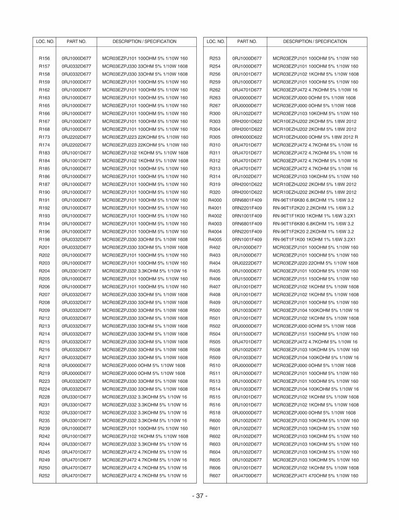
LOC. NO. PART NO. DESCRIPTION / SPECIFICATION
R156
R157
R158
R159
R162
R163
R165
R166
R167
R168
R173
R174
R183
R184
R185
R186
R187
R190
R191
R192
R193
R194
R196
R198
R201
R202
R203
R204
R205
R206
R207
R208
R209
R212
R213
R214
R215
R216
R217
R218
R219
R223
R224
R228
R231
R232
R235
R239
R242
R244
R245
R249
R250
R252
0RJ1000D677
0RJ0332D677
0RJ0332D677
0RJ1000D677
0RJ1000D677
0RJ1000D677
0RJ1000D677
0RJ1000D677
0RJ1000D677
0RJ1000D677
0RJ2202D677
0RJ2202D677
0RJ1001D677
0RJ1001D677
0RJ1000D677
0RJ1000D677
0RJ1000D677
0RJ1000D677
0RJ1000D677
0RJ1000D677
0RJ1000D677
0RJ1000D677
0RJ1000D677
0RJ0332D677
0RJ0332D677
0RJ1000D677
0RJ1000D677
0RJ3301D677
0RJ1000D677
0RJ1000D677
0RJ0332D677
0RJ0332D677
0RJ0332D677
0RJ0332D677
0RJ0332D677
0RJ0332D677
0RJ0332D677
0RJ0332D677
0RJ0332D677
0RJ0000D677
0RJ0000D677
0RJ0332D677
0RJ0332D677
0RJ3301D677
0RJ3301D677
0RJ3301D677
0RJ3301D677
0RJ1000D677
0RJ1001D677
0RJ3301D677
0RJ4701D677
0RJ4701D677
0RJ4701D677
0RJ4701D677
MCR03EZPJ101 100OHM 5% 1/10W 160
MCR03EZPJ330 33OHM 5% 1/10W 1608
MCR03EZPJ330 33OHM 5% 1/10W 1608
MCR03EZPJ101 100OHM 5% 1/10W 160
MCR03EZPJ101 100OHM 5% 1/10W 160
MCR03EZPJ101 100OHM 5% 1/10W 160
MCR03EZPJ101 100OHM 5% 1/10W 160
MCR03EZPJ101 100OHM 5% 1/10W 160
MCR03EZPJ101 100OHM 5% 1/10W 160
MCR03EZPJ101 100OHM 5% 1/10W 160
MCR03EZPJ223 22KOHM 5% 1/10W 160
MCR03EZPJ223 22KOHM 5% 1/10W 160
MCR03EZPJ102 1KOHM 5% 1/10W 1608
MCR03EZPJ102 1KOHM 5% 1/10W 1608
MCR03EZPJ101 100OHM 5% 1/10W 160
MCR03EZPJ101 100OHM 5% 1/10W 160
MCR03EZPJ101 100OHM 5% 1/10W 160
MCR03EZPJ101 100OHM 5% 1/10W 160
MCR03EZPJ101 100OHM 5% 1/10W 160
MCR03EZPJ101 100OHM 5% 1/10W 160
MCR03EZPJ101 100OHM 5% 1/10W 160
MCR03EZPJ101 100OHM 5% 1/10W 160
MCR03EZPJ101 100OHM 5% 1/10W 160
MCR03EZPJ330 33OHM 5% 1/10W 1608
MCR03EZPJ330 33OHM 5% 1/10W 1608
MCR03EZPJ101 100OHM 5% 1/10W 160
MCR03EZPJ101 100OHM 5% 1/10W 160
MCR03EZPJ332 3.3KOHM 5% 1/10W 16
MCR03EZPJ101 100OHM 5% 1/10W 160
MCR03EZPJ101 100OHM 5% 1/10W 160
MCR03EZPJ330 33OHM 5% 1/10W 1608
MCR03EZPJ330 33OHM 5% 1/10W 1608
MCR03EZPJ330 33OHM 5% 1/10W 1608
MCR03EZPJ330 33OHM 5% 1/10W 1608
MCR03EZPJ330 33OHM 5% 1/10W 1608
MCR03EZPJ330 33OHM 5% 1/10W 1608
MCR03EZPJ330 33OHM 5% 1/10W 1608
MCR03EZPJ330 33OHM 5% 1/10W 1608
MCR03EZPJ330 33OHM 5% 1/10W 1608
MCR03EZPJ000 0OHM 5% 1/10W 1608
MCR03EZPJ000 0OHM 5% 1/10W 1608
MCR03EZPJ330 33OHM 5% 1/10W 1608
MCR03EZPJ330 33OHM 5% 1/10W 1608
MCR03EZPJ332 3.3KOHM 5% 1/10W 16
MCR03EZPJ332 3.3KOHM 5% 1/10W 16
MCR03EZPJ332 3.3KOHM 5% 1/10W 16
MCR03EZPJ332 3.3KOHM 5% 1/10W 16
MCR03EZPJ101 100OHM 5% 1/10W 160
MCR03EZPJ102 1KOHM 5% 1/10W 1608
MCR03EZPJ332 3.3KOHM 5% 1/10W 16
MCR03EZPJ472 4.7KOHM 5% 1/10W 16
MCR03EZPJ472 4.7KOHM 5% 1/10W 16
MCR03EZPJ472 4.7KOHM 5% 1/10W 16
MCR03EZPJ472 4.7KOHM 5% 1/10W 16
R253
R254
R256
R259
R262
R263
R267
R300
R303
R304
R305
R310
R311
R312
R313
R314
R319
R320
R4000
R4001
R4002
R4003
R4004
R4005
R402
R403
R404
R405
R406
R407
R408
R409
R500
R501
R502
R504
R505
R508
R509
R510
R511
R513
R514
R515
R516
R518
R600
R601
R602
R603
R604
R605
R606
R607
0RJ1000D677
0RJ1000D677
0RJ1001D677
0RJ1000D677
0RJ4701D677
0RJ0000D677
0RJ0000D677
0RJ1002D677
0RH2001D622
0RH2001D622
0RH0000D622
0RJ4701D677
0RJ4701D677
0RJ4701D677
0RJ4701D677
0RJ1002D677
0RH2001D622
0RH2001D622
0RN6801F409
0RN2201F409
0RN1001F409
0RN6801F409
0RN2201F409
0RN1001F409
0RJ1000D677
0RJ1000D677
0RJ0222D677
0RJ1000D677
0RJ1500D677
0RJ1001D677
0RJ1001D677
0RJ1000D677
0RJ1003D677
0RJ1001D677
0RJ0000D677
0RJ1500D677
0RJ4701D677
0RJ1002D677
0RJ1003D677
0RJ0000D677
0RJ1000D677
0RJ1000D677
0RJ1003D677
0RJ1001D677
0RJ1001D677
0RJ0000D677
0RJ1002D677
0RJ1002D677
0RJ1002D677
0RJ1002D677
0RJ1002D677
0RJ1002D677
0RJ1001D677
0RJ4700D677
MCR03EZPJ101 100OHM 5% 1/10W 160
MCR03EZPJ101 100OHM 5% 1/10W 160
MCR03EZPJ102 1KOHM 5% 1/10W 1608
MCR03EZPJ101 100OHM 5% 1/10W 160
MCR03EZPJ472 4.7KOHM 5% 1/10W 16
MCR03EZPJ000 0OHM 5% 1/10W 1608
MCR03EZPJ000 0OHM 5% 1/10W 1608
MCR03EZPJ103 10KOHM 5% 1/10W 160
MCR10EZHJ202 2KOHM 5% 1/8W 2012
MCR10EZHJ202 2KOHM 5% 1/8W 2012
MCR10EZHJ000 0OHM 5% 1/8W 2012 R
MCR03EZPJ472 4.7KOHM 5% 1/10W 16
MCR03EZPJ472 4.7KOHM 5% 1/10W 16
MCR03EZPJ472 4.7KOHM 5% 1/10W 16
MCR03EZPJ472 4.7KOHM 5% 1/10W 16
MCR03EZPJ103 10KOHM 5% 1/10W 160
MCR10EZHJ202 2KOHM 5% 1/8W 2012
MCR10EZHJ202 2KOHM 5% 1/8W 2012
RN-96T1F6K80 6.8KOHM 1% 1/6W 3.2
RN-96T1F2K20 2.2KOHM 1% 1/6W 3.2
RN-96T1F1K00 1KOHM 1% 1/6W 3.2X1
RN-96T1F6K80 6.8KOHM 1% 1/6W 3.2
RN-96T1F2K20 2.2KOHM 1% 1/6W 3.2
RN-96T1F1K00 1KOHM 1% 1/6W 3.2X1
MCR03EZPJ101 100OHM 5% 1/10W 160
MCR03EZPJ101 100OHM 5% 1/10W 160
MCR03EZPJ220 22OHM 5% 1/10W 1608
MCR03EZPJ101 100OHM 5% 1/10W 160
MCR03EZPJ151 150OHM 5% 1/10W 160
MCR03EZPJ102 1KOHM 5% 1/10W 1608
MCR03EZPJ102 1KOHM 5% 1/10W 1608
MCR03EZPJ101 100OHM 5% 1/10W 160
MCR03EZPJ104 100KOHM 5% 1/10W 16
MCR03EZPJ102 1KOHM 5% 1/10W 1608
MCR03EZPJ000 0OHM 5% 1/10W 1608
MCR03EZPJ151 150OHM 5% 1/10W 160
MCR03EZPJ472 4.7KOHM 5% 1/10W 16
MCR03EZPJ103 10KOHM 5% 1/10W 160
MCR03EZPJ104 100KOHM 5% 1/10W 16
MCR03EZPJ000 0OHM 5% 1/10W 1608
MCR03EZPJ101 100OHM 5% 1/10W 160
MCR03EZPJ101 100OHM 5% 1/10W 160
MCR03EZPJ104 100KOHM 5% 1/10W 16
MCR03EZPJ102 1KOHM 5% 1/10W 1608
MCR03EZPJ102 1KOHM 5% 1/10W 1608
MCR03EZPJ000 0OHM 5% 1/10W 1608
MCR03EZPJ103 10KOHM 5% 1/10W 160
MCR03EZPJ103 10KOHM 5% 1/10W 160
MCR03EZPJ103 10KOHM 5% 1/10W 160
MCR03EZPJ103 10KOHM 5% 1/10W 160
MCR03EZPJ103 10KOHM 5% 1/10W 160
MCR03EZPJ103 10KOHM 5% 1/10W 160
MCR03EZPJ102 1KOHM 5% 1/10W 1608
MCR03EZPJ471 470OHM 5% 1/10W 160
LOC. NO. PART NO. DESCRIPTION / SPECIFICATION
- 37 -
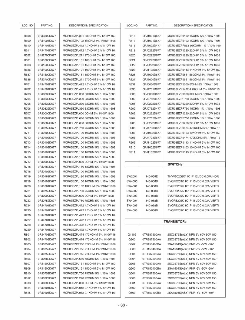
LOC. NO. PART NO. DESCRIPTION / SPECIFICATION
R608
R609
R610
R611
R622
R631
R633
R636
R637
R638
R701
R702
R703
R704
R705
R706
R707
R708
R709
R710
R711
R712
R713
R714
R715
R716
R717
R718
R718
R719
R719
R720
R721
R722
R723
R724
R725
R726
R727
R728
R729
R801
R802
R803
R804
R805
R806
R807
R808
R810
R812
R813
R814
R815
0RJ3300D677
0RJ1001D677
0RJ4701D677
0RJ4701D677
0RJ2700D677
0RJ1000D677
0RJ1500D677
0RJ1000D677
0RJ1500D677
0RJ2700D677
0RJ4701D677
0RJ4701D677
0RJ0332D677
0RJ0332D677
0RJ0332D677
0RJ0332D677
0RJ0000D677
0RJ0682D677
0RJ0682D677
0RJ0752D677
0RJ0102D677
0RJ0102D677
0RJ0102D677
0RJ0102D677
0RJ0102D677
0RJ0102D677
0RJ0000D677
0RJ0182D677
0RJ0102D677
0RJ0182D677
0RJ0102D677
0RJ1001D677
0RJ0752D677
0RJ0000D677
0RJ0752D677
0RJ4701D677
0RJ4701D677
0RJ4701D677
0RJ4701D677
0RJ4701D677
0RJ4701D677
0RJ4703D677
0RJ4703D677
0RJ0752D477
0RJ0752D477
0RJ0752D477
0RJ0682D677
0RJ1500D677
0RJ1500D677
0RJ0752D677
0RJ0222D677
0RJ0000D677
0RJ9101D677
0RJ9101D677
MCR03EZPJ331 330OHM 5% 1/10W 160
MCR03EZPJ102 1KOHM 5% 1/10W 1608
MCR03EZPJ472 4.7KOHM 5% 1/10W 16
MCR03EZPJ472 4.7KOHM 5% 1/10W 16
MCR03EZPJ271 270OHM 5% 1/10W 160
MCR03EZPJ101 100OHM 5% 1/10W 160
MCR03EZPJ151 150OHM 5% 1/10W 160
MCR03EZPJ101 100OHM 5% 1/10W 160
MCR03EZPJ151 150OHM 5% 1/10W 160
MCR03EZPJ271 270OHM 5% 1/10W 160
MCR03EZPJ472 4.7KOHM 5% 1/10W 16
MCR03EZPJ472 4.7KOHM 5% 1/10W 16
MCR03EZPJ330 33OHM 5% 1/10W 1608
MCR03EZPJ330 33OHM 5% 1/10W 1608
MCR03EZPJ330 33OHM 5% 1/10W 1608
MCR03EZPJ330 33OHM 5% 1/10W 1608
MCR03EZPJ000 0OHM 5% 1/10W 1608
MCR03EZPJ680 68OHM 5% 1/10W 1608
MCR03EZPJ680 68OHM 5% 1/10W 1608
MCR03EZPJ750 75OHM 5% 1/10W 1608
MCR03EZPJ100 10OHM 5% 1/10W 1608
MCR03EZPJ100 10OHM 5% 1/10W 1608
MCR03EZPJ100 10OHM 5% 1/10W 1608
MCR03EZPJ100 10OHM 5% 1/10W 1608
MCR03EZPJ100 10OHM 5% 1/10W 1608
MCR03EZPJ100 10OHM 5% 1/10W 1608
MCR03EZPJ000 0OHM 5% 1/10W 1608
MCR03EZPJ180 18OHM 5% 1/10W 1608
MCR03EZPJ100 10OHM 5% 1/10W 1608
MCR03EZPJ180 18OHM 5% 1/10W 1608
MCR03EZPJ100 10OHM 5% 1/10W 1608
MCR03EZPJ102 1KOHM 5% 1/10W 1608
MCR03EZPJ750 75OHM 5% 1/10W 1608
MCR03EZPJ000 0OHM 5% 1/10W 1608
MCR03EZPJ750 75OHM 5% 1/10W 1608
MCR03EZPJ472 4.7KOHM 5% 1/10W 16
MCR03EZPJ472 4.7KOHM 5% 1/10W 16
MCR03EZPJ472 4.7KOHM 5% 1/10W 16
MCR03EZPJ472 4.7KOHM 5% 1/10W 16
MCR03EZPJ472 4.7KOHM 5% 1/10W 16
MCR03EZPJ472 4.7KOHM 5% 1/10W 16
MCR03EZPJ474 470KOHM 5% 1/10W 16
MCR03EZPJ474 470KOHM 5% 1/10W 16
MCR03EZPF750 75OHM 1% 1/10W 1608
MCR03EZPF750 75OHM 1% 1/10W 1608
MCR03EZPF750 75OHM 1% 1/10W 1608
MCR03EZPJ680 68OHM 5% 1/10W 1608
MCR03EZPJ151 150OHM 5% 1/10W 160
MCR03EZPJ151 150OHM 5% 1/10W 160
MCR03EZPJ750 75OHM 5% 1/10W 1608
MCR03EZPJ220 22OHM 5% 1/10W 1608
MCR03EZPJ000 0OHM 5% 1/10W 1608
MCR03EZPJ912 9.1KOHM 5% 1/10W 16
MCR03EZPJ912 9.1KOHM 5% 1/10W 16
R816
R817
R818
R819
R820
R821
R822
R823
R825
R827
R831
R833
R836
R900
R901
R902
R903
R904
R905
R906
R907
R908
R909
R910
R911
SW2001
SW4000
SW4001
SW4002
SW4003
SW4004
SW4005
SW4006
Q1102
Q300
Q302
Q303
Q304
Q304
Q305
Q500
Q501
Q600
Q601
Q602
Q603
0RJ1001D677
0RJ1001D677
0RJ5602D477
0RJ0222D677
0RJ0222D677
0RJ0222D677
0RJ0222D677
0RJ1102D677
0RJ5600D677
0RJ5600D677
0RJ0000D677
0RJ4701D677
0RJ0000D677
0RJ0752D477
0RJ0222D677
0RJ0752D477
0RJ0222D677
0RJ0752D477
0RJ0222D677
0RJ4703D677
0RJ1002D677
0RJ4703D677
0RJ1102D677
0RJ1002D677
0RJ1102D677
140-058E
140-058B
140-058B
140-058B
140-058B
140-058B
140-058B
140-058B
0TR387500AA
0TR387500AA
0TR150400BA
0TR150400BA
0TR387500AA
0TR387500AA
0TR387500AA
0TR150400BA
0TR387500AA
0TR387500AA
0TR387500AA
0TR387500AA
0TR150400BA
MCR03EZPJ102 1KOHM 5% 1/10W 1608
MCR03EZPJ102 1KOHM 5% 1/10W 1608
MCR03EZPF563 56KOHM 1% 1/10W 160
MCR03EZPJ220 22OHM 5% 1/10W 1608
MCR03EZPJ220 22OHM 5% 1/10W 1608
MCR03EZPJ220 22OHM 5% 1/10W 1608
MCR03EZPJ220 22OHM 5% 1/10W 1608
MCR03EZPJ113 11KOHM 5% 1/10W 160
MCR03EZPJ561 560OHM 5% 1/10W 160
MCR03EZPJ561 560OHM 5% 1/10W 160
MCR03EZPJ000 0OHM 5% 1/10W 1608
MCR03EZPJ472 4.7KOHM 5% 1/10W 16
MCR03EZPJ000 0OHM 5% 1/10W 1608
MCR03EZPF750 75OHM 1% 1/10W 1608
MCR03EZPJ220 22OHM 5% 1/10W 1608
MCR03EZPF750 75OHM 1% 1/10W 1608
MCR03EZPJ220 22OHM 5% 1/10W 1608
MCR03EZPF750 75OHM 1% 1/10W 1608
MCR03EZPJ220 22OHM 5% 1/10W 1608
MCR03EZPJ474 470KOHM 5% 1/10W 16
MCR03EZPJ103 10KOHM 5% 1/10W 160
MCR03EZPJ474 470KOHM 5% 1/10W 16
MCR03EZPJ113 11KOHM 5% 1/10W 160
MCR03EZPJ103 10KOHM 5% 1/10W 160
MCR03EZPJ113 11KOHM 5% 1/10W 160
THVV502GBC 1C1P 12VDC 0.05A HORI
EVQPB205K 1C1P 15VDC 0.02A VERTI
EVQPB205K 1C1P 15VDC 0.02A VERTI
EVQPB205K 1C1P 15VDC 0.02A VERTI
EVQPB205K 1C1P 15VDC 0.02A VERTI
EVQPB205K 1C1P 15VDC 0.02A VERTI
EVQPB205K 1C1P 15VDC 0.02A VERTI
EVQPB205K 1C1P 15VDC 0.02A VERTI
2SC3875S(ALY) NPN 5V 60V 50V 150
2SC3875S(ALY) NPN 5V 60V 50V 150
2SA1504S(ASY) PNP -5V -50V -50V
2SA1504S(ASY) PNP -5V -50V -50V
2SC3875S(ALY) NPN 5V 60V 50V 150
2SC3875S(ALY) NPN 5V 60V 50V 150
2SC3875S(ALY) NPN 5V 60V 50V 150
2SA1504S(ASY) PNP -5V -50V -50V
2SC3875S(ALY) NPN 5V 60V 50V 150
2SC3875S(ALY) NPN 5V 60V 50V 150
2SC3875S(ALY) NPN 5V 60V 50V 150
2SC3875S(ALY) NPN 5V 60V 50V 150
2SA1504S(ASY) PNP -5V -50V -50V
LOC. NO. PART NO. DESCRIPTION / SPECIFICATION
- 38 -
SWITCHs
TRANSISTORs
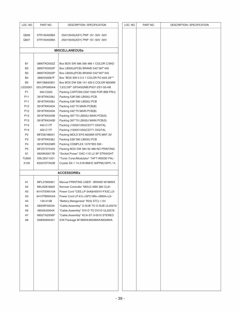
LOC. NO. PART NO. DESCRIPTION / SPECIFICATION
Q606
Q607
B1
B3
B3
B4
B5
LED2001
P1
P11
P11
P12
P12
P13
P13
P14
P14
P2
P3
P4
P5
S1
TU600
X100
A1
A2
A3
A3
A4
A5
A6
A7
A8
0TR150400BA
0TR150400BA
3890TKD002Z
3890TKD002P
3890TKD002P
3890V00067F
MAY36842901
0DLGP0080AA
400-C02Q
3918TKK038J
3918TKK038J
3918TKK040A
3918TKK040A
3918TKK040B
3918TKK040B
400-C17F
400-C17F
MFZ36188501
3918TKK038J
3918TKK038R
MFZ37372403
6620K00017B
EBL35311201
6202VDT002B
MFL37805901
MKJ32816602
6410TEW010A
6410TBW004A
130-013B
68509F0003A
68509J0004A
6852TAZ006P
SAB30693401
2SA1504S(ASY) PNP -5V -50V -50V
2SA1504S(ASY) PNP -5V -50V -50V
Box BOX SW 586 356 486 1 COLOR C/SKD
Box LB500J(PCB) BRAND 542*397*445
Box LB500J(PCB) BRAND 542*397*445
Box "BOX SW 0 0 0 1 COLOR PC-63A 29"""
Box BOX DW 536 141 429 2 COLOR M208W
"LED,DIP" GP34052ME/P507-ZSY-50-HB
Packing CARTON(1200*1000 FOR IBM FRU)
Packing 538*390 LB500J PCB
Packing 538*390 LB500J PCB
Packing 542*70 MAIN PCB(B)
Packing 542*70 MAIN PCB(B)
Packing 397*70 LB500J MAIN PCB(S)
Packing 397*70 LB500J MAIN PCB(S)
Packing (1000X1050)CS771 DIGITAL
Packing (1000X1050)CS771 DIGITAL
Packing MOLD EPS M208W EPS MNT 20'
Packing 538*390 LB500J PCB
Packing COMPLEX 1070*955 SW -
Packing BOX DW 584 50 486 NO PRINTING
"Socket,Power" DAC-11S L2 3P STRAIGHT
"Tuner,Tuner/Modulator" TAFT-W003D PAL-
Crystal SX-1 14.31818MHZ 30PPM(16PF) 14.
Manual PRINTING USER - BRAND M198WA
Remote Controller "MOLD ABS 380 CL81
Power Cord "CEE,LP-34A&H05VV-FX3C,LS-
Power Cord LP-61L+GFC18N+<B90A+LS-
"Battery,Manganese" R03( STC) 1.5V
"Cable,Assembly" D-SUB TO D-SUB UL20276
"Cable,Assembly" DVI-D TO DVI-D UL20276
"Cable,Assembly" KCA-ST-3-0010 STEREO
S/W Package M198WA/M208WA/M228WA
LOC. NO. PART NO. DESCRIPTION / SPECIFICATION
- 39 -
MISCELLANEOUSs
ACCESSORIEs
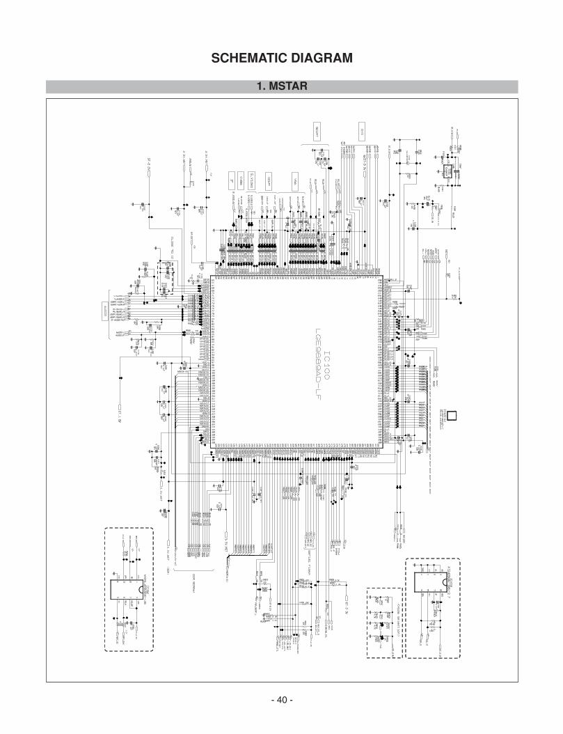
- 40 -
SCHEMATIC DIAGRAM
1. MSTAR
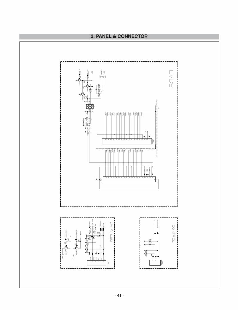
- 41 -
2. PANEL & CONNECTOR
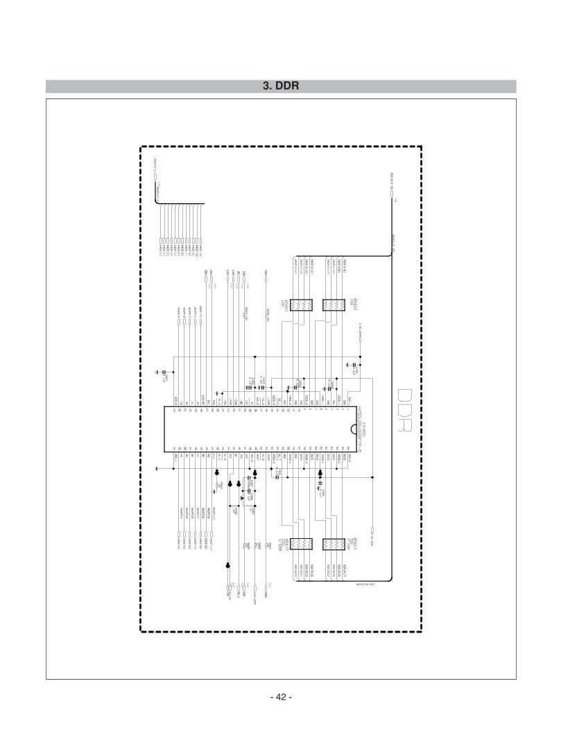
- 42 -
3. DDR
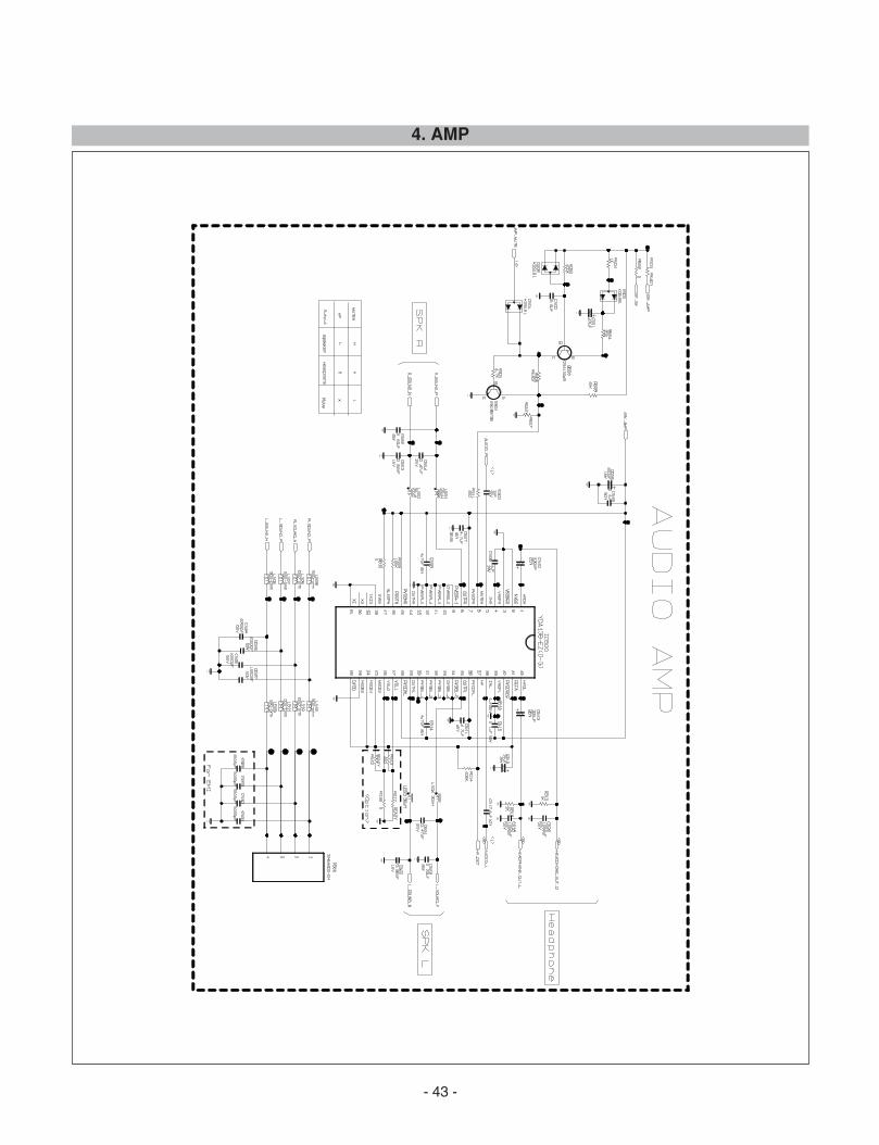
- 43 -
4. AMP
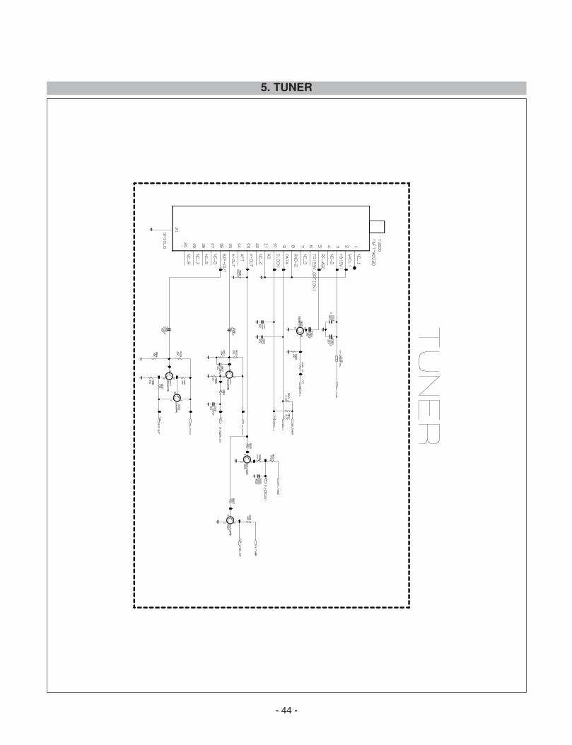
- 44 -
5. TUNER
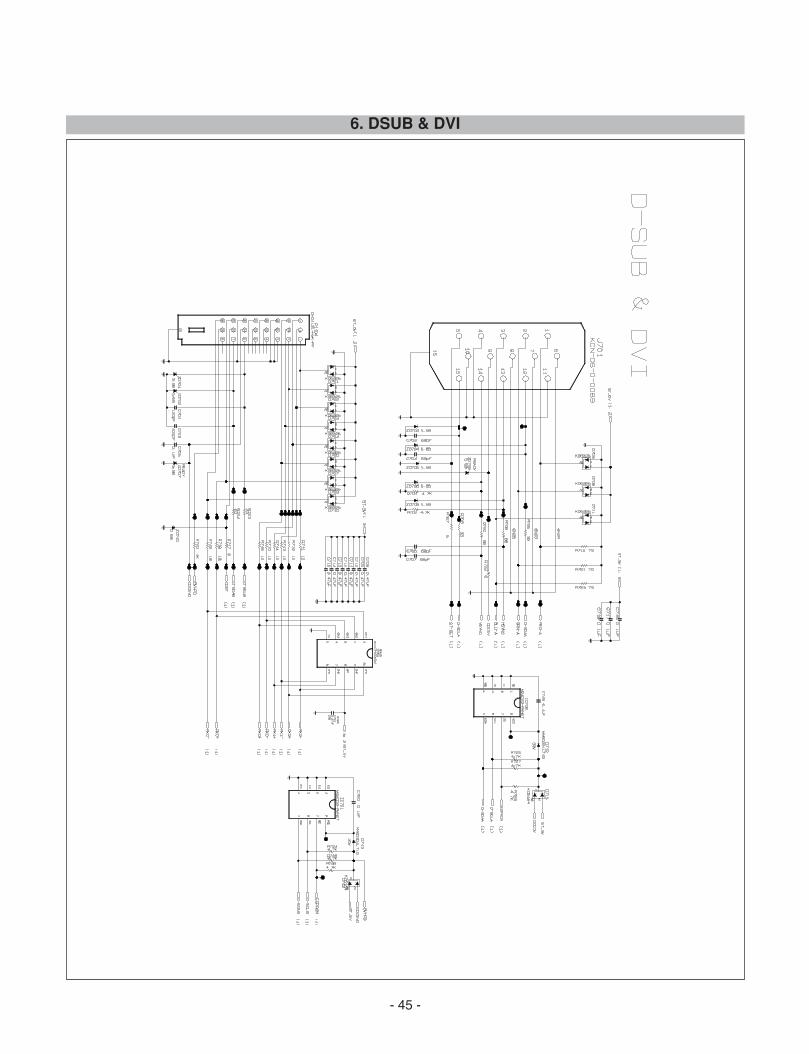
- 45 -
6. DSUB & DVI
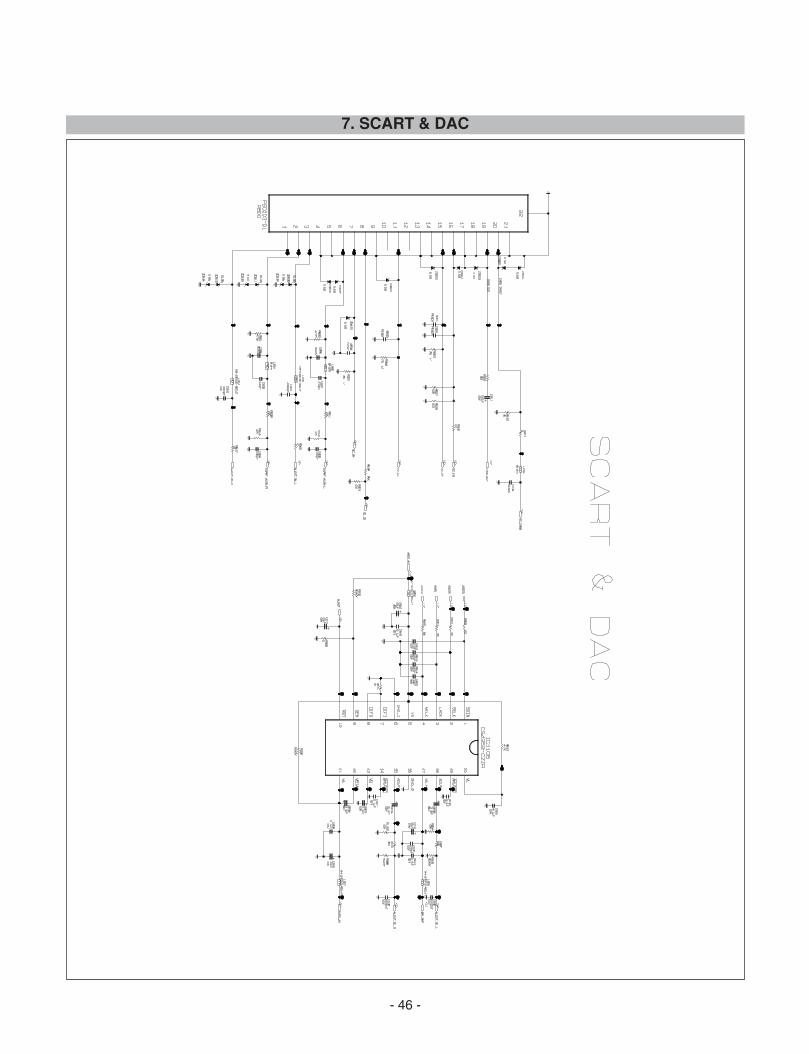
- 46 -
7. SCART & DAC
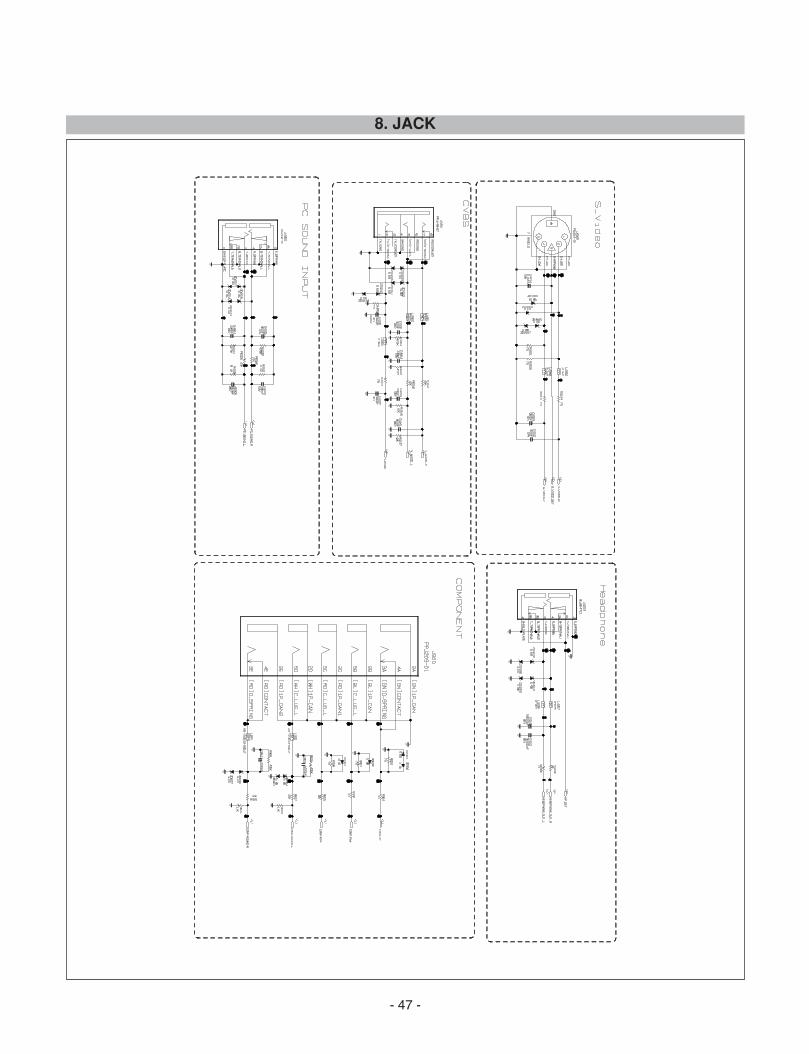
- 47 -
8. JACK
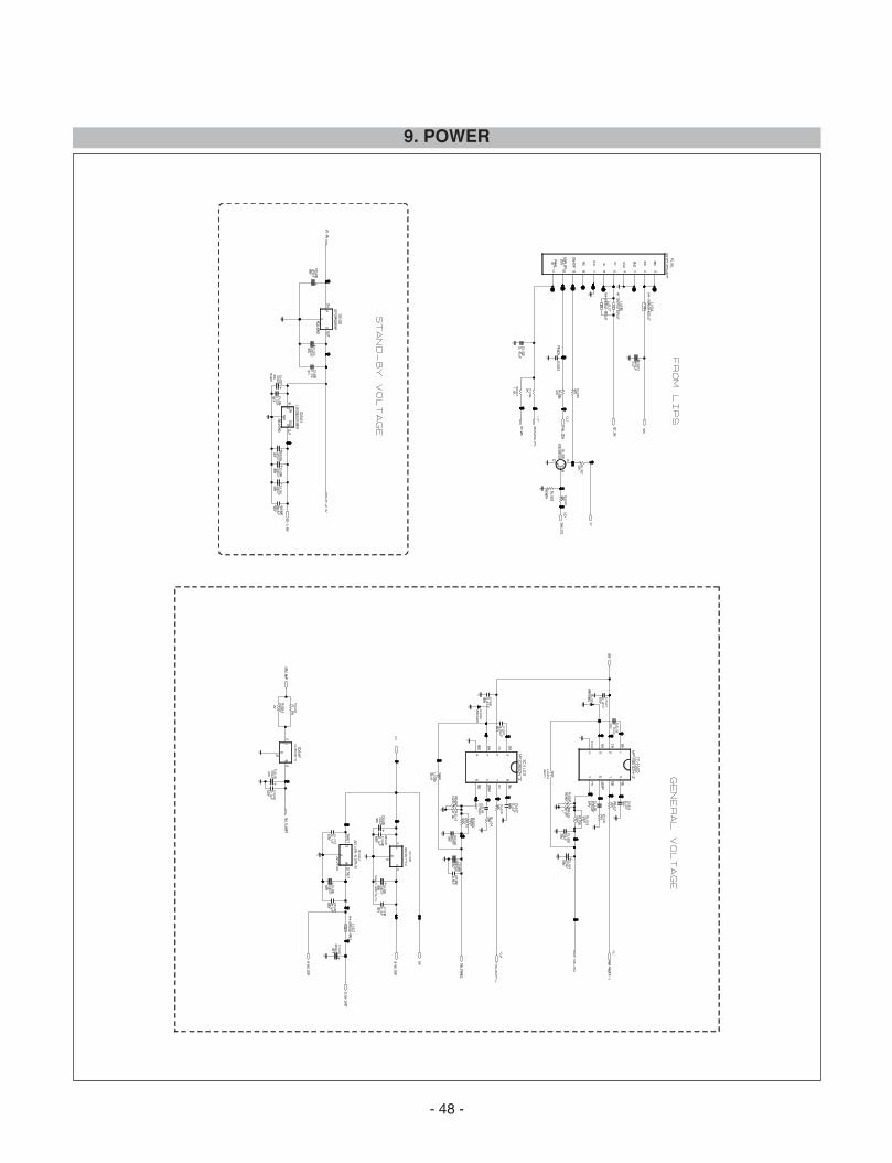
- 48 -
9. POWER
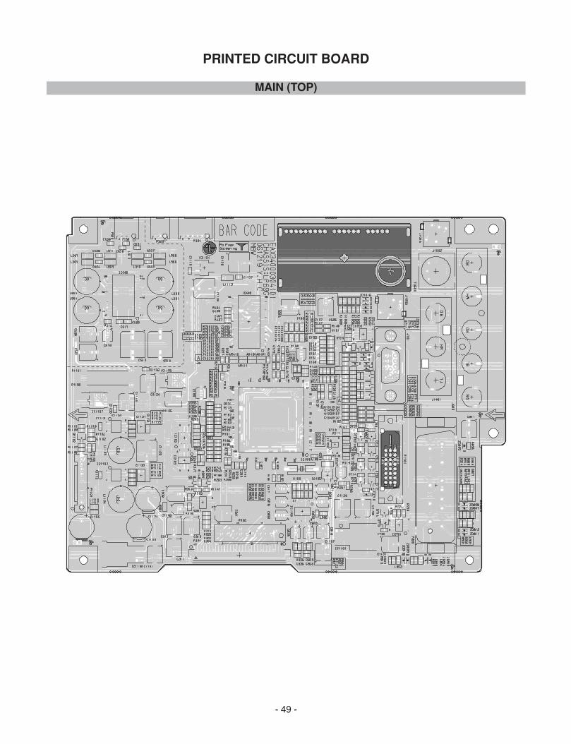
- 49 -
PRINTED CIRCUIT BOARD
MAIN (TOP)
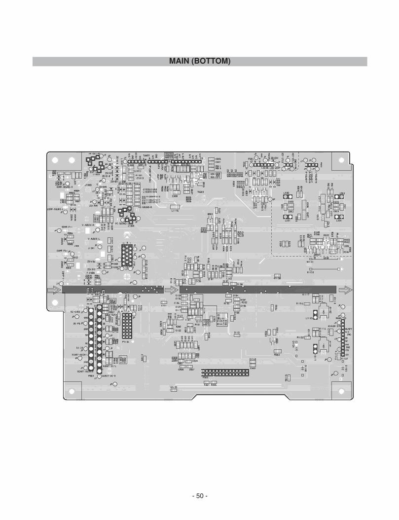
- 50 -
MAIN (BOTTOM)
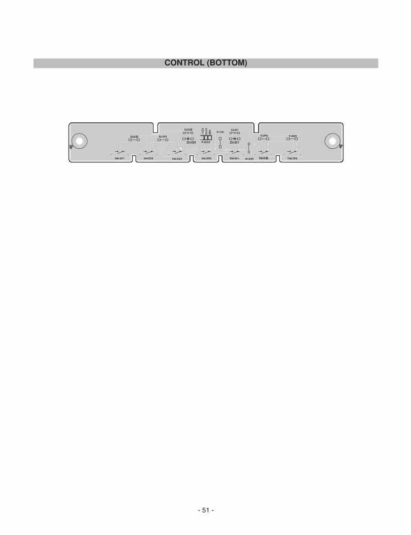
- 51 -
CONTROL (BOTTOM)

Jan. 2007P/NO : MFL36713673 Printed in Korea