Embed Size (px)
Citation preview
Combining soft lithography and functionalmonolayers with electrodeposition to form
nickel and zinc oxide nanostructuresMaster´s thesis
Enne T. FaberEnschede, October 15th 2009Chemical EngineeringUniversity of TwenteFaculty of Science and TechnologyInorganic Materials Science group
Graduation committee Prof. dr. ing. Dave H. A. Blank Dr. ir. André ten Elshof Dr. Regina Luttge Antony George M.Sc.

Abstract
Fabrication techniques for the production of nanostructures were investigated, specifi-cally a combination of microcontact printing, chemical etching, and the electrodepositionof nickel and zinc oxide. Research on electrodeposition at (in some cases exclusively)the sides of structures was performed.
Chemically etching a surface while using a monolayer to protect certain regions ofthe gold substrate from the etchant is a sensitive process. The quality of gold is ofsignificant influence, and the nature of the etchant is very important. Conducting linepatterns have been realized using chemical etching with octadecanethiol as an etch resist,although the monolayer is not intact after the etching step.
The electrodeposition of nickel combines well with microcontact printing based pat-terning, resulting in a smooth nickel layer in the unpatterned regions and cleared areain the patterned regions. The deposition of zinc oxide is less regioselective; most of thedeposit is found in the unpatterned regions while some deposit is found in the patternedregions. The conditions used in this research resulted in a rough deposit.
Deposition on the sides of structures was partially successful. Nickel was deposited ina continuous line along the side of a structure, while zinc oxide deposit could be found ontop of the structure as well. In one test, lines of silver were realized along nickel/gold lineswhich were produced by microcontact printing, etching and electrodeposition. Furtherresearch could include functionalizing surfaces with different monolayers, using etchedfunctionalized structures to deposit other metals, or using a template to deposit zincfeatures in.
i
Contents
1 Goals 11.1 Monolayer as an etch resist . . . . . . . . . . . . . . . . . . . . . . . . . . 21.2 Monolayer as an electrodeposition mask . . . . . . . . . . . . . . . . . . . 21.3 Deposition on the side of structures . . . . . . . . . . . . . . . . . . . . . . 2
2 Theoretical background 32.1 Introduction . . . . . . . . . . . . . . . . . . . . . . . . . . . . . . . . . . . 32.2 Patterning . . . . . . . . . . . . . . . . . . . . . . . . . . . . . . . . . . . . 3
2.2.1 Photolithography . . . . . . . . . . . . . . . . . . . . . . . . . . . . 32.2.2 Microcontact printing and monolayer formation . . . . . . . . . . . 52.2.3 Etching . . . . . . . . . . . . . . . . . . . . . . . . . . . . . . . . . 6
2.3 Electrodeposition . . . . . . . . . . . . . . . . . . . . . . . . . . . . . . . . 62.3.1 Nucleation and growth . . . . . . . . . . . . . . . . . . . . . . . . . 72.3.2 Watt’s bath . . . . . . . . . . . . . . . . . . . . . . . . . . . . . . . 82.3.3 Zinc oxide . . . . . . . . . . . . . . . . . . . . . . . . . . . . . . . . 9
3 Procedures and materials 113.1 Materials . . . . . . . . . . . . . . . . . . . . . . . . . . . . . . . . . . . . 113.2 Silicium wafer cleaning procedure . . . . . . . . . . . . . . . . . . . . . . . 123.3 Gold sputtering procedure . . . . . . . . . . . . . . . . . . . . . . . . . . . 12
3.3.1 Procedure without titanium . . . . . . . . . . . . . . . . . . . . . . 123.3.2 Thin gold layer . . . . . . . . . . . . . . . . . . . . . . . . . . . . . 133.3.3 Heated during sputtering . . . . . . . . . . . . . . . . . . . . . . . 13
3.4 Octadecane thiol monolayer procedure . . . . . . . . . . . . . . . . . . . . 133.5 Etching procedure . . . . . . . . . . . . . . . . . . . . . . . . . . . . . . . 143.6 Nickel electrodeposition procedure . . . . . . . . . . . . . . . . . . . . . . 14
3.6.1 Deposition with higher applied potential . . . . . . . . . . . . . . . 143.6.2 Deposition with more concentrated nickel solution . . . . . . . . . 14
3.7 Zinc oxide electrodeposition procedure . . . . . . . . . . . . . . . . . . . . 153.8 Pre-fabricated photolithography lift-off structures . . . . . . . . . . . . . . 15
3.8.1 Insulation of titanium by fluoride monolayer . . . . . . . . . . . . . 153.9 Combination of techniques . . . . . . . . . . . . . . . . . . . . . . . . . . . 16
4 Results and discussion 184.1 Etching experiments . . . . . . . . . . . . . . . . . . . . . . . . . . . . . . 18
4.1.1 Sputtered gold on titanium . . . . . . . . . . . . . . . . . . . . . . 184.1.2 Functionalized monolayer instead of titanium . . . . . . . . . . . . 194.1.3 Heated sputtered gold . . . . . . . . . . . . . . . . . . . . . . . . . 194.1.4 Sputtered thin gold . . . . . . . . . . . . . . . . . . . . . . . . . . 20
ii
4.1.5 Vapor-deposited gold . . . . . . . . . . . . . . . . . . . . . . . . . . 214.2 Electrodeposition of nickel . . . . . . . . . . . . . . . . . . . . . . . . . . . 22
4.2.1 Nickel deposition with a thiol pattern as a mask . . . . . . . . . . 224.3 Pre-fabricated photolithography lift-off structures . . . . . . . . . . . . . . 23
4.3.1 Insulation by passive oxidation of titanium . . . . . . . . . . . . . 244.3.2 Insulation by fluoride monolayer . . . . . . . . . . . . . . . . . . . 244.3.3 Influence of voltage on nickel nucleation . . . . . . . . . . . . . . . 264.3.4 Influence of nickel ion concentration on nucleation . . . . . . . . . 27
4.4 Electrodeposition of zinc oxide . . . . . . . . . . . . . . . . . . . . . . . . 274.4.1 Zinc oxide deposition using a thiol pattern as a mask . . . . . . . . 274.4.2 Zinc oxide deposition using a prefabricated structure . . . . . . . . 27
4.5 Combination of techniques . . . . . . . . . . . . . . . . . . . . . . . . . . . 28
5 Conclusion and recommendations 305.1 Monolayer as an etch resist . . . . . . . . . . . . . . . . . . . . . . . . . . 305.2 Monolayer as an electrodeposition mask . . . . . . . . . . . . . . . . . . . 305.3 Deposition on the side of structures . . . . . . . . . . . . . . . . . . . . . . 31
Bibliography 31
iii

Foreword
A master project is not something that should be undertaken easily, and a master’s thesisdoesn’t write itself. It is not a five-days experiment or a case study, and it definitelyneeds to be organized to a degree if it is to be successful. While I knew these thingsbefore I started last year, I relearned them so well I feel I have to restate them.
It is hard to oversee all the research one can do in a year beforehand. On the otherhand, after all the research is done it can be difficult to see what is accomplished. Forsomeone with a brain as chaotic as mine, it is very important to add a certain amountof order to the system - this in the form of hypotheses, tests and outcomes, or of coursesimply deadlines. When trying to get something done, I found it very important to havegoals, and to monitor my progress. And when I did get something done, it was usuallyafter asking myself Wait a minute - what do I actually know about this?’. In the end,I feel satisfied - but only partially. There is so much more that can be discovered, somany more tests can be done! However, my time for this has run out, and while I’d loveto see where this subject goes it’s probably not going to be me who does the next part.It is time for me to let go.
Research has left a mixed impression on me. I have always had a dream of becomingan inventor, especially a crazy, somewhat distracted inventor like professor Farnsworthfrom futurama. By now I completely understand why the archetype is like that. Notonly should the inventor bring a degree of order to the chaos that is his mind; he shouldalso be flexible and creative, relaxed and open to new ideas. This is not for everyone,and I hope I’ve got what it takes to carve out some knowledge for the world, or to realizethings that haven’t been done before.
However, I found that I did not much like the practical part of the lab work. Ilike making and disproving theories, thinking up new experiments and analyzing theresults. Perhaps I’d also be one for building models and testing them. I don’t much likemeasuring things in jars or cleaning or trying to get the next test to work the way I wantit to. Still, I think this has taught me the value of the time invested in experiments.While experiments in my mind were always instantly finished and analyzed, in realityeven simple experiments can last days, weeks even. Especially the analytical part. Forthose reasons, it pays to think very well about experiments before even starting them.
In any case, I’m going to do what I always do, be it in sports, studies, socializings orlove - I’m going to throw myself at it and see what happens. To further prepare myselffor the world, I plan to learn in practice. I look for work where I can help with therealization of new things and discover new ideas.
For helping me stay on track with my research, for helping me out practical issues aswell as theoretical problems, I’d like to thank my committee. Anthony, Andre, Regina,Dave - thank you very much. Your guidance gave me some room to breathe in the sheeramount of data and knowledge there is to consider while planning your next experiment.I’d like to thank my girlfriend Anne, my parents and my sister for supporting me in a
iv

time of need and for keeping me going. And finally I’d like to thank everyone who’shelped or motivated me while I was doing my research; the members of the IMS group,my fellow students and friends, as well as Frank Roesthuis and Svetlana Bystrova.
Thank you, everyone. I hope to meet you again in the future - wherever it takes me.Enne Faber
v
Chapter 1
Goals
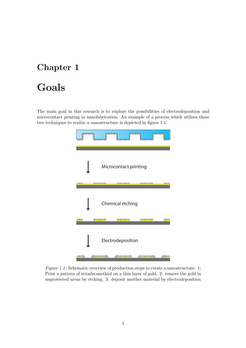
The main goal in this research is to explore the possibilities of electrodeposition andmicrocontact printing in nanofabrication. An example of a process which utilizes thesetwo techniques to realize a nanostructure is depicted in figure 1.1.
Microcontact printing
Chemical etching
Electrodeposition
Figure 1.1: Schematic overview of production steps to create a nanostructure. 1:Print a pattern of octadecanethiol on a thin layer of gold. 2: remove the gold inunprotected areas by etching. 3: deposit another material by electrodeposition
1
1.1 Monolayer as an etch resist
An etch resist is a layer of material deposited, usually in a pattern, onto a substrate. Thematerials under the etch resist are protected from any etchants, so that if any etchingoccurs it only occurs in the unprotected areas. In most cases, an etch resist is a polymer,with a pattern produced by photolithography.
Using octadecanethiol, it may be possible to use only a single layer of highly orderedmolecules as an effective etch resist. Such a such a layer could already effectively pro-tect the underlying material. Monolayers of octadecanethiol can be produced by softlithography.
If this proves effective and easy to use, this also means that soft lithography could beused to apply such resists quickly and cheaply, providing an alternative to conventionalphotolithography. If such a layer manages to be an effective resist and the attainablefeature size is sufficiently small, this would be interesting for a number of applications.
1.2 Monolayer as an electrodeposition mask
Electrodeposition (or electroplating) is commonly used in the industry to form coatingsor contacts of one or more metal layers on a surface. In conventional electroplating, itis very important to keep the surface clean because even small traces of dirt or organicscan strongly affect the quality of the plating. In this research, this property is exploredas a tool, using monolayer patterns in an attempt to selectively prevent deposition on apart of the surface.
Electrodeposition has previously been used to create nanostructures using templatessuch as channels. However, to use an open structure with only a monolayer to con-trol the formation of structures is an entirely new challenge which may also offer newopportunities.
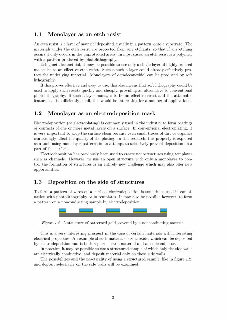
1.3 Deposition on the side of structures
To form a pattern of wires on a surface, electrodeposition is sometimes used in combi-nation with photolithography or in templates. It may also be possible however, to forma pattern on a nonconducting sample by electrodeposition.
Figure 1.2: A structure of patterned gold, covered by a nonconducting material
This is a very interesting prospect in the case of certain materials with interestingelectrical properties. An example of such materials is zinc oxide, which can be depositedby electrodeposition and is both a piezoelectric material and a semiconductor.
In practice, it may be possible to use a structured sample of which only the side wallsare electrically conductive, and deposit material only on these side walls.
The possibilities and the practicality of using a structured sample, like in figure 1.2,and deposit selectively on the side walls will be examined.
2
Chapter 2
Theoretical background
2.1 Introduction
Micro- and nanostructures have a stunning number of uses these days [1,2]. Not onlyare such structures used in electronics as wiring, transistors and memory chips - nanos-tructures are also used in completely different applications like sensors. An interestingconcept which has enjoyed a lot of attention the last few years is that of the microreactorand even the lab-on-a-chip.
Photolithography is the most commonly used technique to produce micro- and nanos-tructures. Photolithography is a well-developed technique, however it is important toknow what alternative patterning techniques can be used and what the possibilitiesand limitations of such techniques are. Some techniques have advantages over othertechniques when it comes to implementation; whether that is higher efficiency, smallerattainable feature size or even new options. Additional development of patterning tech-niques will open new opportunities and allow us to produce more - for less.
2.2 Patterning
Transistors in electronics are generally fabricated by depositing a pattern of conductingmaterial (copper, gold or other metals and/or metallic materials) onto a monocrystallinesilicon substrate. Sensors come in a wide variety of applications, and as such consist ofa wide variety of materials.
Examples of patterning techniques can be found in table 2.1 [3].One of the major advantages of making the features of a device very small is that a
large amount of functional units (transistors, memory cells, sensor cells or even simpleconducting lines) can be realized using a minimal amount of space and material. To dothis effectively, a master pattern is first created. The master is then used to transfer andreplicate the pattern.
Using photolithography as an example, a master pattern comes in the shape of alithographic mask. This mask is used many times to transfer the pattern to the pho-toresist.
2.2.1 Photolithography
Photolithography is the most commonly used method to realize nanostructures, by com-bining it with deposition and/or etch techniques. A thin film of resist is deposited onthe substrate, generally by spin coating. Light of a specific wavelength (in combination
3
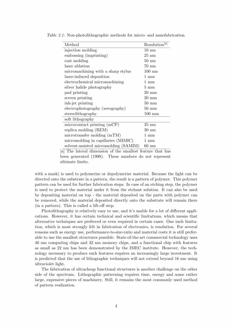
Table 2.1: Non-photolithographic methods for micro- and nanofabrication.
Method Resolution[a]
injection molding 10 nmembossing (imprinting) 25 nmcast molding 50 nmlaser ablation 70 nmmicromachining with a sharp stylus 100 nmlaser-induced deposition 1 mmelectrochemical micromachining 1 mmsilver halide photography 5 mmpad printing 20 mmscreen printing 20 mmink-jet printing 50 mmelectrophotography (xerography) 50 mmstereolithography 100 mm
soft lithography
microcontact printing (mCP) 35 nmreplica molding (REM) 30 nmmicrotransfer molding (mTM) 1 mmmicromolding in capillaries (MIMIC) 1 mmsolvent-assisted micromolding (SAMIM) 60 nm
[a] The lateral dimension of the smallest feature that hasbeen generated (1998). These numbers do not representultimate limits.
with a mask) is used to polymerize or depolymerize material. Because the light can bedirected onto the substrate in a pattern, the result is a pattern of polymer. This polymerpattern can be used for further fabrication steps. In case of an etching step, the polymeris used to protect the material under it from the etchant solution. It can also be usedby depositing material on top - the material deposited on the parts with polymer canbe removed, while the material deposited directly onto the substrate will remain there(in a pattern). This is called a lift-off step.
Photolithography is relatively easy to use, and it’s usable for a lot of different appli-cations. However, it has certain technical and scientific limitations, which means thatalternative techniques are preferred or even required in certain cases. One such limita-tion, which is most strongly felt in fabrication of electronics, is resolution. For severalreasons such as energy use, performance-to-size-ratio and material costs it is still prefer-able to use the smallest structures possible. State-of-the-art commercial technology uses40 nm computing chips and 32 nm memory chips, and a functional chip with featuresas small as 22 nm has been demonstrated by the IMEC institute. However, the tech-nology necessary to produce such features requires an increasingly large investment. Itis predicted that the use of lithographic techniques will not extend beyond 16 nm usingultraviolet light.
The fabrication of ultracheap functional structures is another challenge on the otherside of the spectrum. Lithographic patterning requires time, energy and some ratherlarge, expensive pieces of machinery. Still, it remains the most commonly used methodof pattern realization.
4
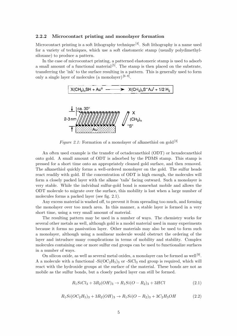
2.2.2 Microcontact printing and monolayer formation
Microcontact printing is a soft lithography technique [4]. Soft lithography is a name usedfor a variety of techniques, which use a soft elastomeric stamp (usually polydimethyl-siloxane) to produce a pattern.
In the case of microcontact printing, a patterned elastomeric stamp is used to adsorba small amount of a functional material [5]. The stamp is then placed on the substrate,transferring the ’ink’ to the surface resulting in a pattern. This is generally used to formonly a single layer of molecules (a monolayer) [6–8].
Figure 2.1: Formation of a monolayer of alkanethiol on gold [3]
An often used example is the transfer of octadecanethiol (ODT) or hexadecanethiolonto gold. A small amount of ODT is adsorbed by the PDMS stamp. This stamp ispressed for a short time onto an appropriately cleaned gold surface, and then removed.The alkanethiol quickly forms a well-ordered monolayer on the gold. The sulfur headsreact readily with gold. If the concentration of ODT is high enough, the molecules willform a closely packed layer with the alkane ’tails’ facing outward. Such a monolayer isvery stable. While the indvidual sulfur-gold bond is somewhat mobile and allows theODT molecule to migrate over the surface, this mobility is lost when a large number ofmolecules forms a packed layer (see fig. 2.1).
Any excess material is washed off, to prevent it from spreading too much, and formingthe monolayer over too much area. In this manner, a stable layer is formed in a veryshort time, using a very small amount of material.
The resulting pattern may be used in a number of ways. The chemistry works forseveral other metals as well, although gold is a model material used in many experimentsbecause it forms no passivation layer. Other materials may also be used to form sucha monolayer, although using a nonlinear molecule would obstruct the ordering of thelayer and intruduce many complications in terms of mobility and stability. Complexmolecules containing one or more sulfur end groups can be used to functionalize surfacesin a number of ways.
On silicon oxide, as well as several metal oxides, a monolayer can be formed as well [9].A a molecule with a functional -Si(OC2H5)3 or -SiCl3 end group is required, which willreact with the hydroxide groups at the surface of the material. These bonds are not asmobile as the sulfur bonds, but a closely packed layer can still be formed.
R1SiCl3 + 3R2(OH)3 → R1Si(O −R2)3 + 3HCl (2.1)
R1Si(OC2H5)3 + 3R2(OH)3 → R1Si(O −R2)3 + 3C2H5OH (2.2)
5
These reactions can be performed in a reflux setup, or in some cases from vaporphase in low vacuum.
2.2.3 Etching
Etching is a technique often used in micro- and nanofabrication in combination withphotolithography. There are two kinds of etching - chemical etching and plasma etching.In both cases, a part of the surface is protected (usually in by a pattern of material)while a part is exposed and etched. The chemical etchant or the plasma removes theexposed material. In this way, a pattern of material can be preserved while the rest isremoved, effectively forming a structure on the substrate.
In chemical etching the material is removed by a chemical reaction, usually in a fuidenvironment. Anodic and cathodic etching (which are forms of chemical etching) allowthe material to be dissolved by an oxidation or reduction reaction, respectively. Plasmaetching uses an ionized gas (usually oxygen or argon) to bombard the surface and removesmall pieces of material.
It is possible to use a very thin layer of material, such as an ordered alkanethiolmonolayer as a resist for a chemical etching process. Some research [10–12] is being doneon this subject. However, the selectivity of the etch rate is very important for the successof this technique.
Which etching methods are effective at removing material depends entirely on thematerial to be removed [13]. Because there are so many different etching agents, andthe etching process can be finely controlled, etching is an often-used instrument in thefabrication of microstructures.
In this research, oxygen plasma is used to clean traces of organic matter off thesurface of substrates, as well as to aid in the accelerated formation of passivating oxidelayers on titanium or nickel. Chemical etching is used as well, to selectively remove goldfrom a gold layer. This etchant does not remove nickel, which adds some opportunitiesthat will be used later on.
2.3 Electrodeposition
Electrodeposition is a method by which a layer of material can be deposited from asolution onto a conducting surface.
In this research, metallic nickel and zinc oxide are deposited from solution. Certainother metals can be deposited in a manner very similar to nickel, making this a flexibletechnique [15]. Also, like zinc oxide some nonmetallic materials can be deposited fromsolution by electrodeposition.
Conventional electrodeposition uses a reduction half reaction to turn metal ions insolution into solid metal. Electrons are needed for this reaction, and so the metal reducesat the cathode according to halfreaction 2.3, and deposits there. Meanwhile, anotherhalf reaction (usually the production of oxygen according to halfreaction 2.3) takes placeat the anode.
Mn+ + ne− →M0(s) (2.3)
4OH− → 2H2O +O2 + 4e− (2.4)
Because the reaction requires electrons, it can be assumed that the deposited materialwill be present on the conducting parts of the cathode, and not on the nonconducting
6
-
+
+
++
+
-
-
--
-+Anode
Anion
Ref erence electrode
Cathode
Cation
Electrolyte
+-
E ref
Electrochemical cell
anode(counter)
cathode(working)
reference
(a) (b)
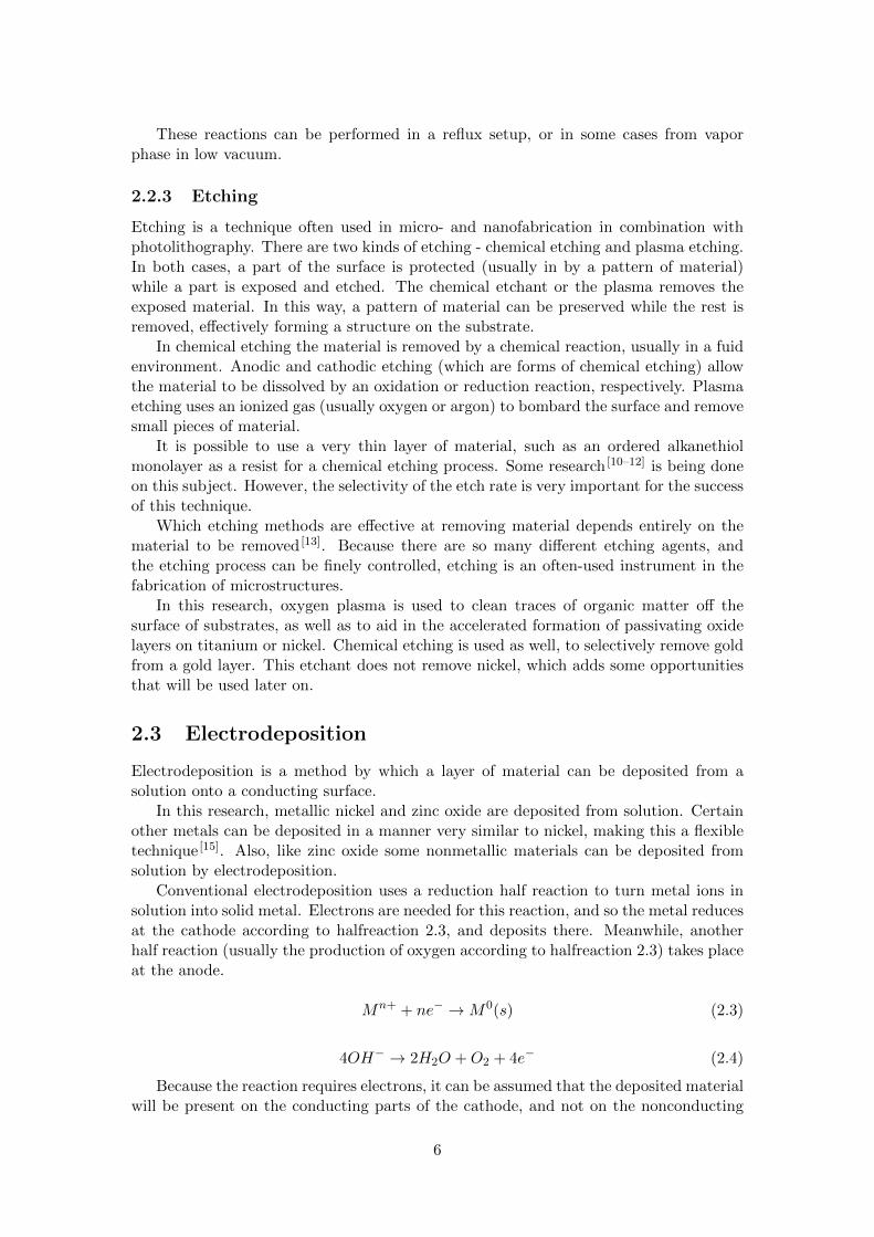
Figure 2.2: (a) A three-electrode setup (b) 3-electrode schematic [14]
parts. While electroplating in practice, it is found that even small contaminations such asfingerprints can easily stain the resulting layer of metal, indicating that the depositionis a sensitive process. Some research has indicated this can be used by performingelectrodeposition in combination with a monolayer [16]. The deposition of zinc oxide(which is also practiced in this research) is more complicated, and will be decribed inmore detail below.
It is possible to do electrodeposition using only two electrodes; one is the cathodeand one is the anode. However, both for metal and for metal oxide deposition, a threeelectrode setup is used. A schematic of a three-electrode setup is given in figure 2.2. Inthe setup used in this research, a silver chloride reference electrode is used. No currentflows through it, and the potential of the reference electrode is determined by reaction2.5 at V0 = 0,22 V.
AgCl(s) + e− ↔ Ag(s) + Cl−(aq) (2.5)
The advantages of adding the reference electrode to the setup, is that there is muchmore control over the potential of each electrode. This gives and therefore over theprocesses occurring at the electrodes.
2.3.1 Nucleation and growth
Deposition of metals is generally a two-phase process [17–20].First, insoluble metal is created and it nucleates on the surface. It forms small
pockets of material, with a preference for rougher surfaces and certain geometric features.Forming a nucleite requires a significant amount of energy, due to the high curvatureand the high surface-to-size ratio of the new pocket of material. Interfacial tension is avery important factor. In cases where the interfacial tension between the substrate andthe growing material is very low, nucleation may be a negligible part of the process.
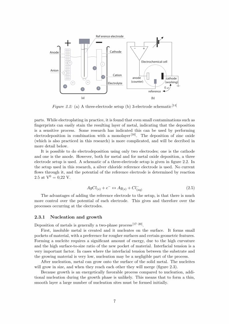
After nucleation, metal can grow onto the surface of the solid metal. The nucleiteswill grow in size, and when they reach each other they will merge (figure 2.3).
Because growth is an energetically favorable process compared to nucleation, addi-tional nucleation during the growth phase is unlikely. This means that to form a thin,smooth layer a large number of nucleation sites must be formed initially.
7
cba
Figure 2.3: Schematic of nucleation and growth phases. (a) Before deposition(b) Nucleation phase (c) Growth phase
2.3.2 Watt’s bath
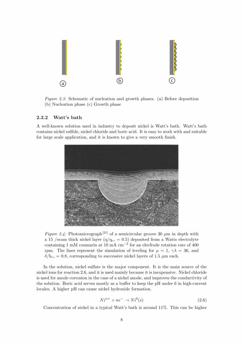
A well-known solution used in industry to deposit nickel is Watt’s bath. Watt’s bathcontains nickel sulfide, nickel chloride and boric acid. It is easy to work with and suitablefor large scale application, and it is known to give a very smooth finish.
Figure 2.4: Photomicrograph [21] of a semicircular groove 30 �m in depth witha 15 /mum thick nickel layer (q/q∘, = 0.5) deposited from a Watts electrolytecontaining 1 mM coumarin at 10 mA cm−2 for an elecfrode rotation rate of 400rpm. The lines represent the simulation of leveling for � = 1, � = 36, and�/h∘, = 0.8, corresponding to successive nickel layers of 1.5 �m each.
In the solution, nickel sulfate is the major component. It is the main source of thenickel ions for reaction 2.6, and it is used mainly because it is inexpensive. Nickel chlorideis used for anode corrosion in the case of a nickel anode, and improves the conductivity ofthe solution. Boric acid serves mostly as a buffer to keep the pH under 6 in high-currentlocales. A higher pH can cause nickel hydroxide formation.
Nin+ + ne− → Ni0(s) (2.6)
Concentration of nickel in a typical Watt’s bath is around 11%. This can be higher
8
or lower, depending on the needs of the application. Higher current density requires ahigher nickel flux, so the bath needs a higher nickel ion concentration for example.
Other customizations include the addition of organic brighteners or certain additivesto achieve specific results. A range of options is available when choosing the concentra-tions and additives in the solution. For example, changing the concentration of chlorideand sulfide influences the brightness of the deposit. In general deposits produced usingWatt’s contain sulfur - which may be avoided by adding certain organic agents.
An additional effect (which may contribute to the brightness of said layers) is ob-served by Madore and Landolt [21,22]. As the metal layer is being deposited, it quicklyforms a closed layer. Any initial pits and gaps are quickly filled with nickel while theprotruding parts grow relatively slowly (see figure 2.4).
2.3.3 Zinc oxide
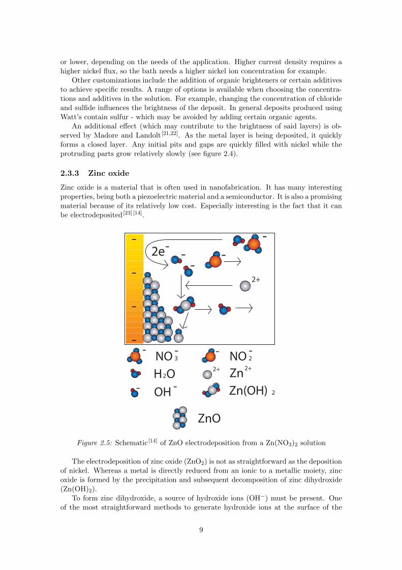
Zinc oxide is a material that is often used in nanofabrication. It has many interestingproperties, being both a piezoelectric material and a semiconductor. It is also a promisingmaterial because of its relatively low cost. Especially interesting is the fact that it canbe electrodeposited [23] [14].
-
-
-
-
---
-2+
2e-
H2O
- NO 3-
- OH -
- NO 2-
2+ Zn2+
ZnO
Zn(OH) 2
Figure 2.5: Schematic [14] of ZnO electrodeposition from a Zn(NO3)2 solution
The electrodeposition of zinc oxide (ZnO2) is not as straightforward as the depositionof nickel. Whereas a metal is directly reduced from an ionic to a metallic moiety, zincoxide is formed by the precipitation and subsequent decomposition of zinc dihydroxide(Zn(OH)2).
To form zinc dihydroxide, a source of hydroxide ions (OH−) must be present. Oneof the most straightforward methods to generate hydroxide ions at the surface of the
9
electrode is the half reaction 2.7. The freshly formed hydroxide ions will react with anynearby zinc ions according to reaction 2.8.
NO−3 +H2O + 2e− → NO−
2 + 2OH− (2.7)
Zn2+ + 2OH− → Zn(OH)2 (2.8)
The zinc hydroxide complex is only slightly soluble in water, and in larger concen-trations will precipitate. The electrode is covered in nonconducting zinc hydroxide. Atelevated temperatures (60-90∘C) the hydroxide will decompose, forming zinc oxide ac-cording to reaction 2.9. Since the hydroxide ions are being formed near the surface ofthe electrode, the most likely place for the zinc oxide to form is on the electrode.
Zn(OH)2 → ZnO +H2O (2.9)
As a result, a solution of zinc nitrate can be used to form zinc oxide by electrodeposi-tion. Deposition conditions can be varied to tune the morphology and properties of theformed zinc oxide layer, however experiments in this research were mostly preliminaryand so the conditions were mostly kept constant.
Important parameters which can be used to tune and control the behaviour of thereaction and the properties of the resulting deposit include acidity, temperature, voltage,current density and the option of exciting the solution using stirrers or bubbles.
10
Chapter 3
Procedures and materials
3.1 Materials
The materials and specialized equipment used in this research were the following:
∙ Sputtered gold - gold sputtered on location using a Perkin-Elmer sputter machinemodel 2400
∙ Atomic force microscope - Veeco Dimension Icon
∙ Silicon wafers - p-type silicon wafers from OKMETIC
∙ Nickel sulphate hexahydrate, Sigma-Aldrich, 227676 - 1 kg
∙ Boric acid, Sigma-Aldrich, 339067 - 500g
∙ Silver nitrate, Acros, 419351000
∙ Zinc nitrate, Sigma-Aldrich, 228737-500g
∙ Nitric acid, Acros, 12460010 - 1 l
∙ Nickel compatible gold etchant, Aldrich, 651842 - 500 ml1
∙ 1-octadecanethiol, Aldrich, 01858 - 25 ml
∙ Trichloro-(1H,1H,2H,2H-perfluorooctyl)silane 97% pure, Aldrich, 448931 - 10 g
∙ (3-mercaptopropyl)trimethoxysilane, Fluka, 63800 - 100 ml
∙ Absolute ethanol, Assink Chemie - 5 l
∙ Samples of 20 nm gold evaporated onto glass - ordered from SSENS
∙ Potentioscan Wenking POS 73
1Contains 5-10% iodine, 10-20% potassium iodide, 5-10% (NH4)2HPO4 (diammonium hydrophos-phate)
11
3.2 Silicium wafer cleaning procedure
Silicium wafers are first cleaned with purified ethanol. The alcohol is blown off withnitrogen, and the wafer is placed on a heater. While it is kept on the heater, a jet ofhigh pressure carbon dioxide gas is blown over it. The crystals are assumed to removeall traces of organic matter, as well as any remaining dust particles. In some cases, thesilicium is also treated with a piranha solution (3 parts sulfuric acid, 1 part hydrogenperoxide) for 15 minutes.
3.3 Gold sputtering procedure
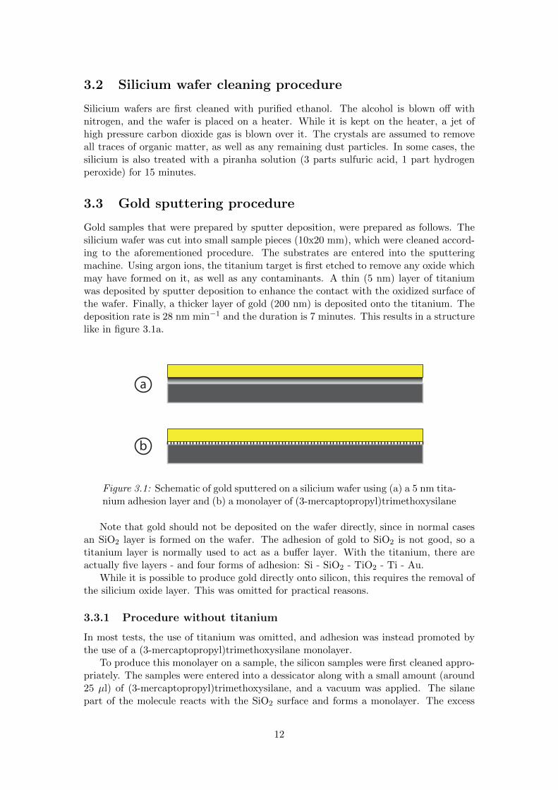
Gold samples that were prepared by sputter deposition, were prepared as follows. Thesilicium wafer was cut into small sample pieces (10x20 mm), which were cleaned accord-ing to the aforementioned procedure. The substrates are entered into the sputteringmachine. Using argon ions, the titanium target is first etched to remove any oxide whichmay have formed on it, as well as any contaminants. A thin (5 nm) layer of titaniumwas deposited by sputter deposition to enhance the contact with the oxidized surface ofthe wafer. Finally, a thicker layer of gold (200 nm) is deposited onto the titanium. Thedeposition rate is 28 nm min−1 and the duration is 7 minutes. This results in a structurelike in figure 3.1a.
a
b
Figure 3.1: Schematic of gold sputtered on a silicium wafer using (a) a 5 nm tita-nium adhesion layer and (b) a monolayer of (3-mercaptopropyl)trimethoxysilane
Note that gold should not be deposited on the wafer directly, since in normal casesan SiO2 layer is formed on the wafer. The adhesion of gold to SiO2 is not good, so atitanium layer is normally used to act as a buffer layer. With the titanium, there areactually five layers - and four forms of adhesion: Si - SiO2 - TiO2 - Ti - Au.
While it is possible to produce gold directly onto silicon, this requires the removal ofthe silicium oxide layer. This was omitted for practical reasons.
3.3.1 Procedure without titanium
In most tests, the use of titanium was omitted, and adhesion was instead promoted bythe use of a (3-mercaptopropyl)trimethoxysilane monolayer.
To produce this monolayer on a sample, the silicon samples were first cleaned appro-priately. The samples were entered into a dessicator along with a small amount (around25 �l) of (3-mercaptopropyl)trimethoxysilane, and a vacuum was applied. The silanepart of the molecule reacts with the SiO2 surface and forms a monolayer. The excess
12
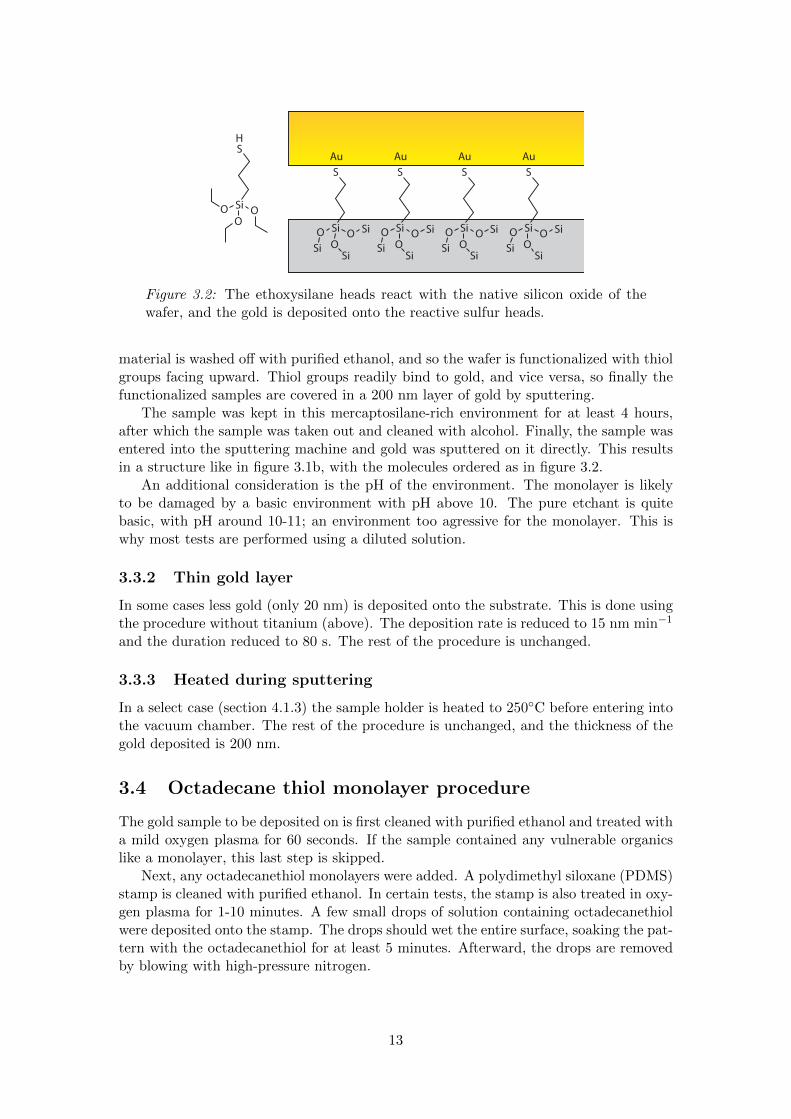
Figure 3.2: The ethoxysilane heads react with the native silicon oxide of thewafer, and the gold is deposited onto the reactive sulfur heads.
material is washed off with purified ethanol, and so the wafer is functionalized with thiolgroups facing upward. Thiol groups readily bind to gold, and vice versa, so finally thefunctionalized samples are covered in a 200 nm layer of gold by sputtering.
The sample was kept in this mercaptosilane-rich environment for at least 4 hours,after which the sample was taken out and cleaned with alcohol. Finally, the sample wasentered into the sputtering machine and gold was sputtered on it directly. This resultsin a structure like in figure 3.1b, with the molecules ordered as in figure 3.2.
An additional consideration is the pH of the environment. The monolayer is likelyto be damaged by a basic environment with pH above 10. The pure etchant is quitebasic, with pH around 10-11; an environment too agressive for the monolayer. This iswhy most tests are performed using a diluted solution.
3.3.2 Thin gold layer
In some cases less gold (only 20 nm) is deposited onto the substrate. This is done usingthe procedure without titanium (above). The deposition rate is reduced to 15 nm min−1
and the duration reduced to 80 s. The rest of the procedure is unchanged.
3.3.3 Heated during sputtering
In a select case (section 4.1.3) the sample holder is heated to 250∘C before entering intothe vacuum chamber. The rest of the procedure is unchanged, and the thickness of thegold deposited is 200 nm.
3.4 Octadecane thiol monolayer procedure
The gold sample to be deposited on is first cleaned with purified ethanol and treated witha mild oxygen plasma for 60 seconds. If the sample contained any vulnerable organicslike a monolayer, this last step is skipped.
Next, any octadecanethiol monolayers were added. A polydimethyl siloxane (PDMS)stamp is cleaned with purified ethanol. In certain tests, the stamp is also treated in oxy-gen plasma for 1-10 minutes. A few small drops of solution containing octadecanethiolwere deposited onto the stamp. The drops should wet the entire surface, soaking the pat-tern with the octadecanethiol for at least 5 minutes. Afterward, the drops are removedby blowing with high-pressure nitrogen.
13
The dried stamp is placed onto the gold sample. A very small amount of pressure isapplied to ensure full contact. After 10-60 seconds, the stamp is removed and the goldsample is cleaned again with purified ethanol; this time to remove any excess thiol.
Re-use of PDMS stamps should yield the same results as using fresh stamps for eachexperiment, especially if the stamp is not treated with an oxygen plasma. However, freshstamps are used each time to eliminate this as a possible unknown.
Octadecane thiol monolayers and patterns on gold are considered quite stable. How-ever, if more than a day has passed since the deposition of such a layer, the layer isremoved (by plasma) and a new layer is deposited in its stead. The use of old andpossibly degraded patterns is avoided to eliminate this as a possible unknown.
To promote the affinity between the PDMS and the alcoholic ink solution, PDMSstamps can be treated with oxygen plasma for a short time. This forms an oxide layeron the outside of the stamp. However, preliminary experiments showed that this reducesthe friction between the PDMS and the gold, making it more difficult to produce a clearpattern without moving the stamp over the surface. Oxidizing the stamp was omittedin further experiments.
3.5 Etching procedure
In certain experiments, an etch step was used to remove gold. The sample to be etchedwas cleaned with alcohol, and an etching solution was produced from the nickel selectiveetchant obtained from Aldrich. Three different concentrations were used for this solution:the pure etchant, a solution of 20% etchant with 80% demineralized water and a solutionof 5% etchant with 95% demineralized water.
The substrate is placed in the beaker with etching solution for the appropriateamount of time. No stirring or excitation of the fluid was performed. After etching,the sample is taken out and flushed with demineralized water.
3.6 Nickel electrodeposition procedure
In each of these experiments a solution of 0,91 M nickel sulphate and 0,58 M boric acidis used unless specifically noted otherwise. Most were produced with either a carbonor platina counter electrode, and a silver chloride reference electrode. Deposition isperformed at the cathode at -1 V (direct current) relative to the reference electrode.
Before deposition, the sample is positioned with the connection to the cathode abovethe surface. The parts of the surface where deposition is desired are submerged. Then,the potential is applied for a specified time (depending on the experiment). Finally, thesample is removed from the solution and flushed in demineralized water.
3.6.1 Deposition with higher applied potential
Tests were performed with a higher applied potential. The potential was -10 V (DC)relative to the reference electrode, and all other parameters remained the same.
3.6.2 Deposition with more concentrated nickel solution
Tests were also performed with a more concentrated solution. The concentration ofnickel is increased to 1,8 M and excess boric acid was added (up to the solubility of 0,76M at room temperature). The applied potential was -1 V (DC) relative to the referenceelectrode.
14
3.7 Zinc oxide electrodeposition procedure
For the deposition of zinc oxide, a beaker containing a 10,0 mM solution of zinc nitratewas used at 70 ∘C. The deposition occured at the cathode, and deposition was executedat -1 V relative to the reference electrode. Only direct current is used.
Before deposition, the solution is heated up to 70 ∘C. The sample is connected to thecathode, and the cathode is positioned so that the areas where deposition is desired aresubmerged. The potential of -1 V is applied for a specified time, and finally the sampleis removed and flushed in demineralized water.
3.8 Pre-fabricated photolithography lift-off structures
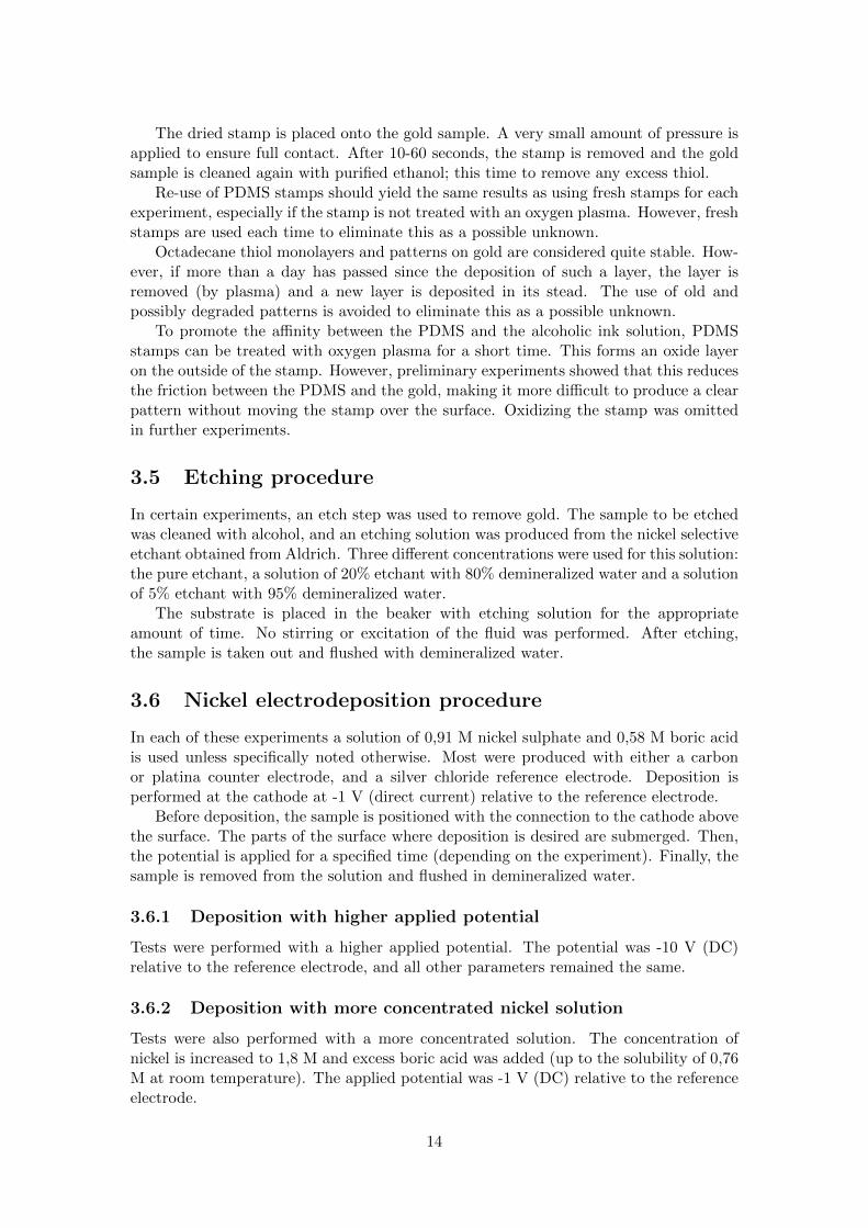
In order to allow the testing of material deposition on the side walls of structures,independent from the result of other parts of the research, samples were produced bySvetlana Bystrova from the Mesoscale Chemical Systems group.
Figure 3.3: Structure produced by photolithography and lift-off. From bottomto top the materials are: Oxidized silicium wafer, 5 nm titanium, 100 nm gold,10 nm titanium.
A 200 nm layer of photoresist was applied to a cleaned and oxidized silicon wafer.The layer was patterned and the excess resist washed off. Using sputter deposition,the following materials were deposited onto the patterned wafer consecutively: 5 nm oftitanium, 100 nm gold, 10 nm titanium. The bottom layer of titanium serves to promoteadhesion to the oxidized silicon, the gold is the functional conductor and the top layerof titanium is to be oxidized and possibly functionalized as an insulator.
Finally, the photoresist pattern was used to lift off a pattern in the sample by ultra-sonication of the wafer in acetone. Theoretically, the resulting structure should corre-spond to figure 3.3.
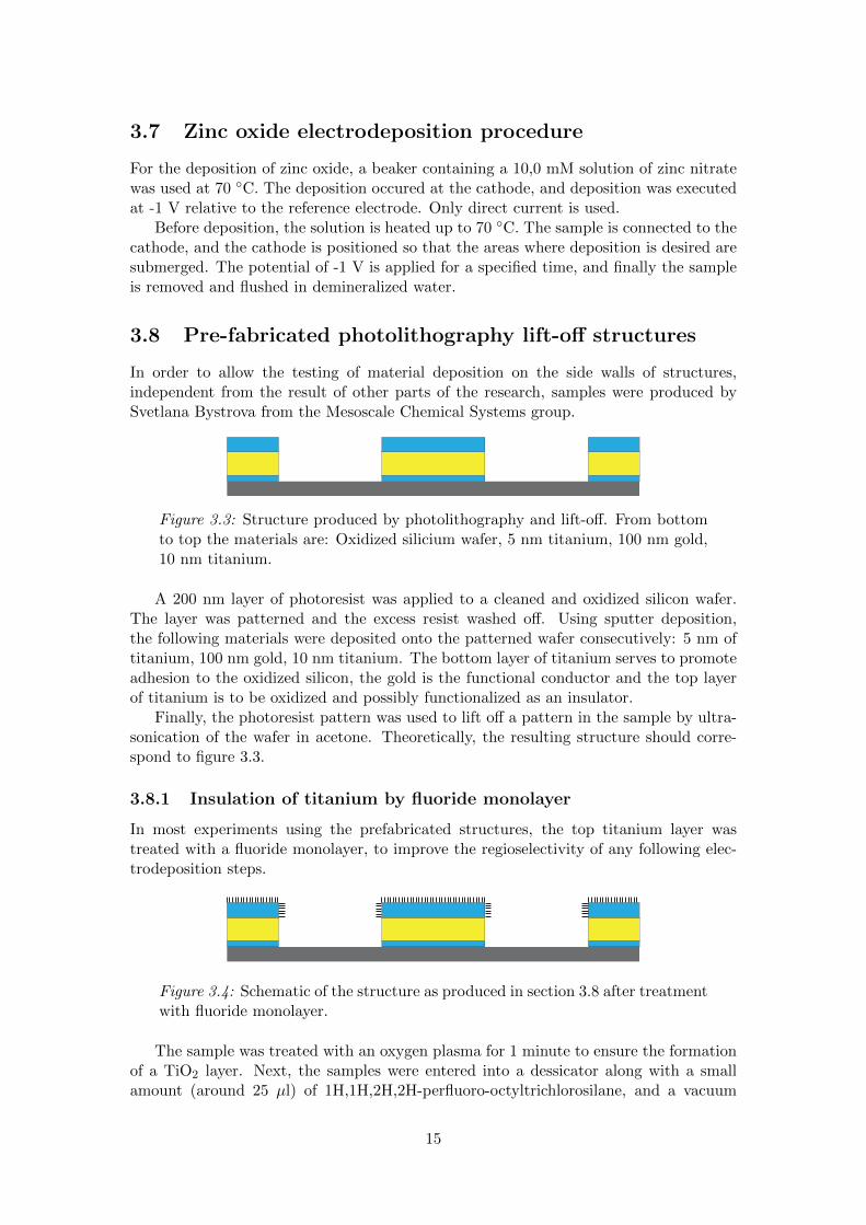
3.8.1 Insulation of titanium by fluoride monolayer
In most experiments using the prefabricated structures, the top titanium layer wastreated with a fluoride monolayer, to improve the regioselectivity of any following elec-trodeposition steps.
Figure 3.4: Schematic of the structure as produced in section 3.8 after treatmentwith fluoride monolayer.
The sample was treated with an oxygen plasma for 1 minute to ensure the formationof a TiO2 layer. Next, the samples were entered into a dessicator along with a smallamount (around 25 �l) of 1H,1H,2H,2H-perfluoro-octyltrichlorosilane, and a vacuum
15
was applied. In this vacuum, the functional material evaporates. The silane part of themolecule reacts with the TiO2 surface and forms a monolayer, quite similar to section3.3.1. The excess material is washed off with purified ethanol.
in the following manner. A pre-fabricated structure (as described before) was treatedby a mild oxygen plasma to clean it and ensure the top titanium layer is oxidized. Thesample was placed in a dessicator, and a few drops of 1H,1H,2H,2H-perfluoro-octyl-trichlorosilane were added (without making direct contact). The air was pumped out ofthe dessicator, and in the resulting vacuum some of the functional monolayer is expectedto evaporate. The sample was kept in the resulting low-pressure atmosphere for at least4 hours, and then removed from the vacuum chamber and cleaned with purified alcohol.
3.9 Combination of techniques
An experiment was conducted to test the reliability and wuality of the structures pro-duced by electrodepostion, soft lithography and etching. In this test, no lithography isused, and the entire series of experiments was executed on a single sample. An overviewof the process can be seen in figure 3.5. The sample used was a 20 nm vapor depositedgold sample as delivered by SSENS. After each step is a cleaning step with demineralizedwater and with ethanol.
Microcontact printing
A pattern of octadecanethiol lines was deposited on the gold surface using a PDMSstamp (see section 3.4)
Nickel electrodeposition
A 60 nm layer of nickel was deposited on the unpatterned areas by electrodeposition(see section 3.6)
Etching with nickel as a resist
An alternative was used to etch the aforementioned patterns into the gold. Because theetchant does not remove nickel a process as depicted in figure 3.5 may be possible. Anickel layer could be used as an etch resist, after being produced on the gold in a patternby electrodepostion.
The resulting sample was treated in an oxygen plasma for 1 minute to remove thethiol. An etching step was performed as in section 3.5. The total etching time was 50seconds, performed in two steps because after 25 seconds a residual gold layer could stillbe found.
Monolayer deposition
The sample was treated with an oxygen plasma again to ensure that the outside ofthe nickel layer was oxidized. The sample was treated with a 1H,1H,2H,2H-perfluoro-octyltrichlorosilane monolayer as in section 3.8.1.
Silver electrodeposition
The nickel layer should now be nonconductive, while the gold underneath is conducting.When placed in a solution, the gold is in contact with the solution at the sides, so
16
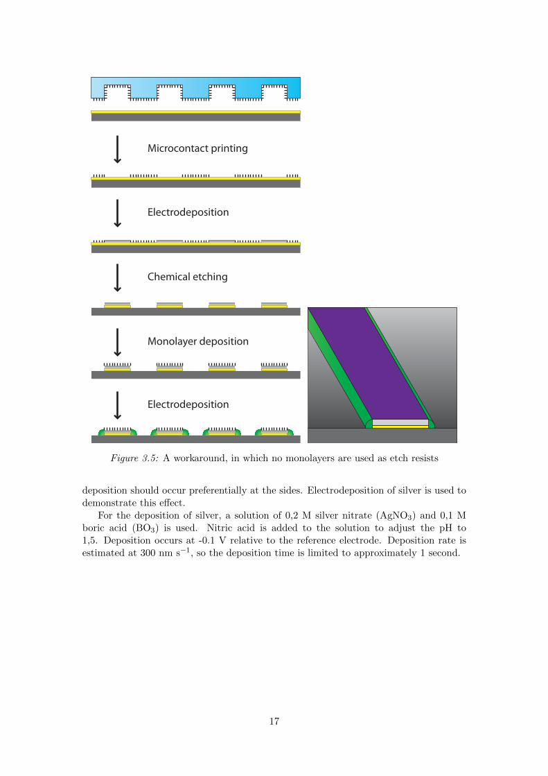
Microcontact printing
Chemical etching
Electrodeposition
Electrodeposition
Monolayer deposition
Figure 3.5: A workaround, in which no monolayers are used as etch resists
deposition should occur preferentially at the sides. Electrodeposition of silver is used todemonstrate this effect.
For the deposition of silver, a solution of 0,2 M silver nitrate (AgNO3) and 0,1 Mboric acid (BO3) is used. Nitric acid is added to the solution to adjust the pH to1,5. Deposition occurs at -0.1 V relative to the reference electrode. Deposition rate isestimated at 300 nm s−1, so the deposition time is limited to approximately 1 second.
17
Chapter 4
Results and discussion
4.1 Etching experiments
The etch rate of the etchant solution was determined beforehand by etching a layers ofgold with known thickness, and measuring the required time.
For removing a 200 nm sputtered/annealed gold layer in the 100% etchant solution,the time required was 30 seconds. After 25 seconds, some gold could still be fount onthe surface. The etch rate was estimated at 7 nm s−1.
Removing 200 nm sputtered/annealed gold in the 20% etchant diluted with deminer-alized water required close to 4 minutes or 240 seconds. 200 seconds was not enough toremove all the gold. The etch rate was estimated around 0,9 nm s−1.
Removing 20 nm vapor-deposited gold in the 5% etchant diluted with demineralizedwater required 50-60 seconds. The etch rate was estimated 0,3-0,4 nm s−1.
In short, these preliminary tests revealed that the etch rates were approximately thefollowing:
1. 100% etchant: 6,7 nm s−1
2. 20% etchant: 0,9 nm s−1
3. 5% etchant: 0,35 nm s−1
4.1.1 Sputtered gold on titanium
Gold layers were produced using titanium adhesion layers as described in section 3.3.These samples were etched for 30 seconds in 100% pure gold etchant. However, theadhesion of the gold to the substrate proved insufficient. During the etching step, thegold was separated from the substrate.
When etching the gold, the adhesion of the gold layer to the silicium proved unreli-able. The partially intact gold layer would be released from the substrate and float inthe solution. It is unknown whether this is a problem with the titanium adhesion layer,the etching solution, or something different. It may be that the titanium or titaniumoxide in the buffer layer (both needed for adhesion) were etched by the etchant similarto the gold. However the patterns created with a octadecanethiol monolayer were beingetched into the gold to an extent, as could be observed with a microscope.
18
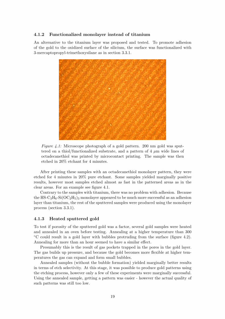
4.1.2 Functionalized monolayer instead of titanium
An alternative to the titanium layer was proposed and tested. To promote adhesionof the gold to the oxidized surface of the silicium, the surface was functionalized with3-mercaptopropyl-trimethoxysilane as in section 3.3.1.
Figure 4.1: Microscope photograph of a gold pattern. 200 nm gold was sput-tered on a thiol/functionalized substrate, and a pattern of 4 �m wide lines ofoctadecanethiol was printed by microcontact printing. The sample was thenetched in 20% etchant for 4 minutes.
After printing these samples with an octadecanethiol monolayer pattern, they wereetched for 4 minutes in 20% pure etchant. Some samples yielded marginally positiveresults, however most samples etched almost as fast in the patterned areas as in theclear areas. For an example see figure 4.1.
Contrary to the samples with titanium, there was no problem with adhesion. Becausethe HS-C3H6-Si(OC2H5)3 monolayer appeared to be much more successful as an adhesionlayer than titanium, the rest of the sputtered samples were produced using the monolayerprocess (section 3.3.1).
4.1.3 Heated sputtered gold
To test if porosity of the sputtered gold was a factor, several gold samples were heatedand annealed in an oven before testing. Annealing at a higher temperature than 300∘C could result in a gold layer with bubbles protruding from the surface (figure 4.2).Annealing for more than an hour seemed to have a similar effect.
Presumably this is the result of gas pockets trapped in the pores in the gold layer.The gas builds up pressure, and because the gold becomes more flexible at higher tem-peratures the gas can expand and form small bubbles.
Annealed samples (without the bubble formation) yielded marginally better resultsin terms of etch selectivity. At this stage, it was possible to produce gold patterns usingthe etching process, however only a few of these experiments were marginally successful.Using the annealed sample, getting a pattern was easier - however the actual quality ofsuch patterns was still too low.
19
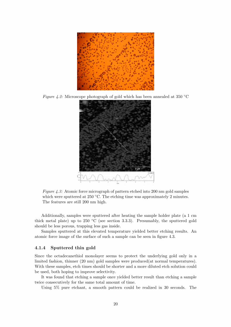
Figure 4.2: Microscope photograph of gold which has been annealed at 350 ∘C
Figure 4.3: Atomic force micrograph of pattern etched into 200 nm gold sampleswhich were sputtered at 250 ∘C. The etching time was approximately 2 minutes.The features are still 200 nm high.
Additionally, samples were sputtered after heating the sample holder plate (a 1 cmthick metal plate) up to 250 ∘C (see section 3.3.3). Presumably, the sputtered goldshould be less porous, trapping less gas inside.
Samples sputtered at this elevated temperature yielded better etching results. Anatomic force image of the surface of such a sample can be seen in figure 4.3.
4.1.4 Sputtered thin gold
Since the octadecanethiol monolayer seems to protect the underlying gold only in alimited fashion, thinner (20 nm) gold samples were produced(at normal temperatures).With these samples, etch times should be shorter and a more diluted etch solution couldbe used, both hoping to improve selectivity.
It was found that etching a sample once yielded better result than etching a sampletwice consecutively for the same total amount of time.
Using 5% pure etchant, a smooth pattern could be realized in 30 seconds. The
20
pattern is not very beautiful, and may not be continuous. Conducting lines (4,6 Ohm)were realized, although the lines are very rough and most of the gold is removed. There isa electrically conductive residual layer, and it is not likely this could be removed withoutalso removing the gold pattern.
Also, a pattern of gold could be realized using the 20% pure etchant for 4-5 seconds,although etching for 5-6 seconds would also cause the remaining gold to dissolve. Suchpatterns were not conductive.
4.1.5 Vapor-deposited gold
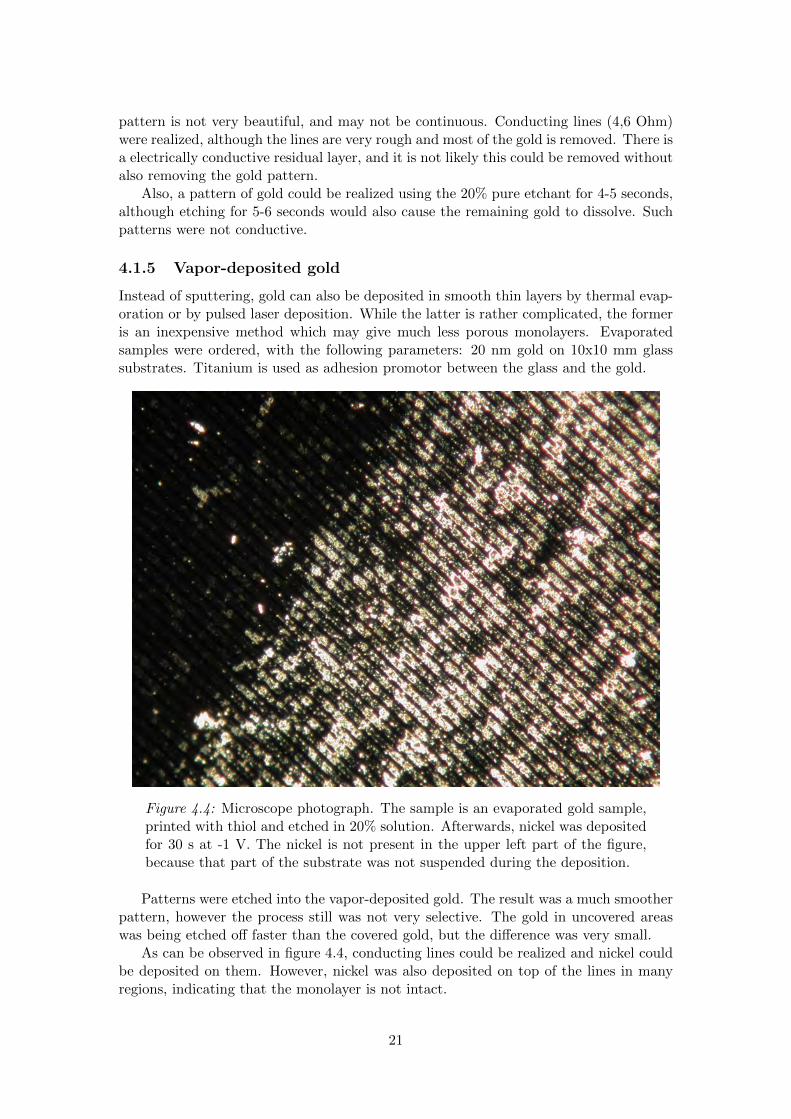
Instead of sputtering, gold can also be deposited in smooth thin layers by thermal evap-oration or by pulsed laser deposition. While the latter is rather complicated, the formeris an inexpensive method which may give much less porous monolayers. Evaporatedsamples were ordered, with the following parameters: 20 nm gold on 10x10 mm glasssubstrates. Titanium is used as adhesion promotor between the glass and the gold.
Figure 4.4: Microscope photograph. The sample is an evaporated gold sample,printed with thiol and etched in 20% solution. Afterwards, nickel was depositedfor 30 s at -1 V. The nickel is not present in the upper left part of the figure,because that part of the substrate was not suspended during the deposition.
Patterns were etched into the vapor-deposited gold. The result was a much smootherpattern, however the process still was not very selective. The gold in uncovered areaswas being etched off faster than the covered gold, but the difference was very small.
As can be observed in figure 4.4, conducting lines could be realized and nickel couldbe deposited on them. However, nickel was also deposited on top of the lines in manyregions, indicating that the monolayer is not intact.
21
4.2 Electrodeposition of nickel
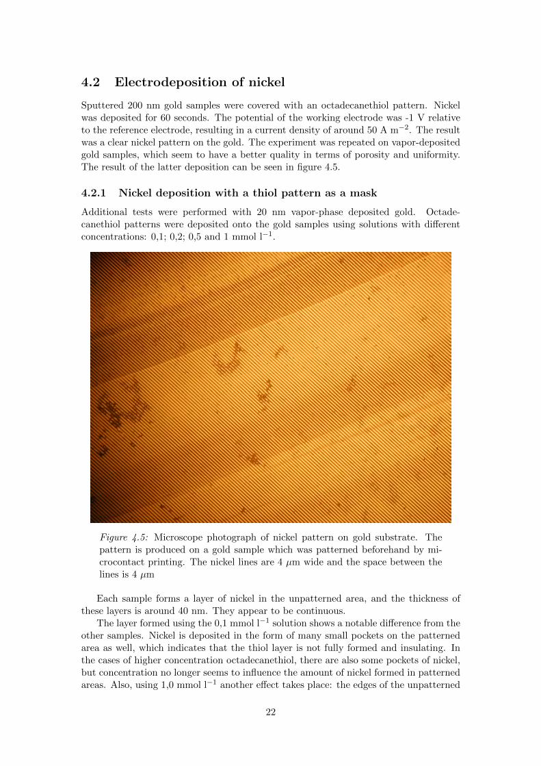
Sputtered 200 nm gold samples were covered with an octadecanethiol pattern. Nickelwas deposited for 60 seconds. The potential of the working electrode was -1 V relativeto the reference electrode, resulting in a current density of around 50 A m−2. The resultwas a clear nickel pattern on the gold. The experiment was repeated on vapor-depositedgold samples, which seem to have a better quality in terms of porosity and uniformity.The result of the latter deposition can be seen in figure 4.5.
4.2.1 Nickel deposition with a thiol pattern as a mask
Additional tests were performed with 20 nm vapor-phase deposited gold. Octade-canethiol patterns were deposited onto the gold samples using solutions with differentconcentrations: 0,1; 0,2; 0,5 and 1 mmol l−1.
Figure 4.5: Microscope photograph of nickel pattern on gold substrate. Thepattern is produced on a gold sample which was patterned beforehand by mi-crocontact printing. The nickel lines are 4 �m wide and the space between thelines is 4 �m
Each sample forms a layer of nickel in the unpatterned area, and the thickness ofthese layers is around 40 nm. They appear to be continuous.
The layer formed using the 0,1 mmol l−1 solution shows a notable difference from theother samples. Nickel is deposited in the form of many small pockets on the patternedarea as well, which indicates that the thiol layer is not fully formed and insulating. Inthe cases of higher concentration octadecanethiol, there are also some pockets of nickel,but concentration no longer seems to influence the amount of nickel formed in patternedareas. Also, using 1,0 mmol l−1 another effect takes place: the edges of the unpatterned
22
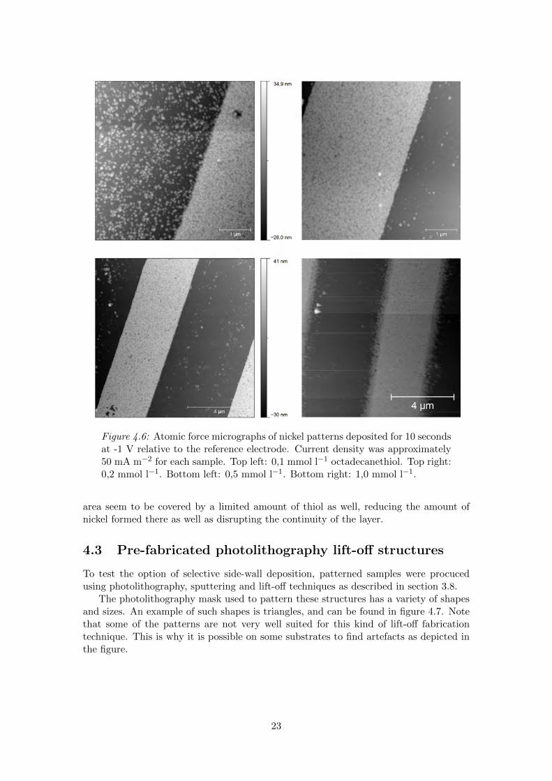
Figure 4.6: Atomic force micrographs of nickel patterns deposited for 10 secondsat -1 V relative to the reference electrode. Current density was approximately50 mA m−2 for each sample. Top left: 0,1 mmol l−1 octadecanethiol. Top right:0,2 mmol l−1. Bottom left: 0,5 mmol l−1. Bottom right: 1,0 mmol l−1.
area seem to be covered by a limited amount of thiol as well, reducing the amount ofnickel formed there as well as disrupting the continuity of the layer.
4.3 Pre-fabricated photolithography lift-off structures
To test the option of selective side-wall deposition, patterned samples were procucedusing photolithography, sputtering and lift-off techniques as described in section 3.8.
The photolithography mask used to pattern these structures has a variety of shapesand sizes. An example of such shapes is triangles, and can be found in figure 4.7. Notethat some of the patterns are not very well suited for this kind of lift-off fabricationtechnique. This is why it is possible on some substrates to find artefacts as depicted inthe figure.
23
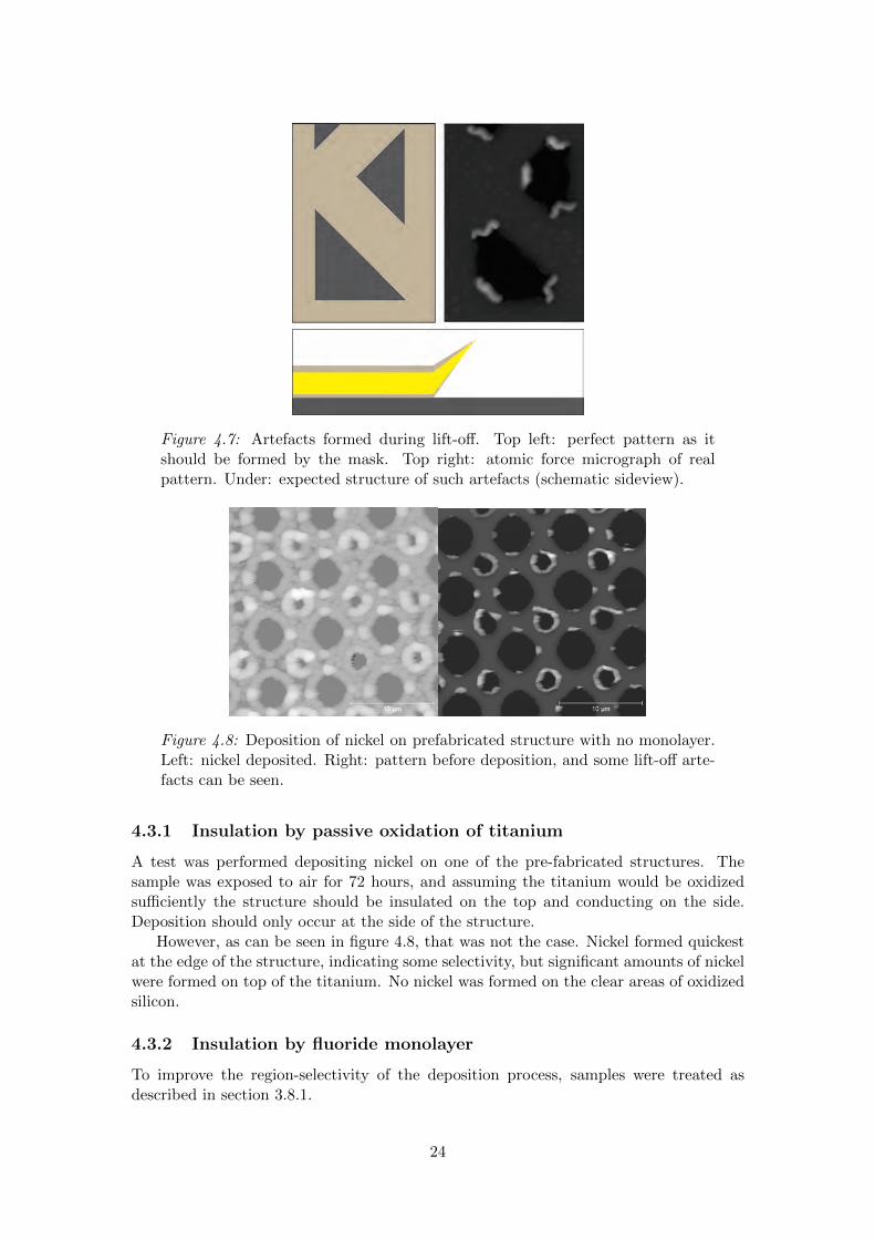
Figure 4.7: Artefacts formed during lift-off. Top left: perfect pattern as itshould be formed by the mask. Top right: atomic force micrograph of realpattern. Under: expected structure of such artefacts (schematic sideview).
Figure 4.8: Deposition of nickel on prefabricated structure with no monolayer.Left: nickel deposited. Right: pattern before deposition, and some lift-off arte-facts can be seen.
4.3.1 Insulation by passive oxidation of titanium
A test was performed depositing nickel on one of the pre-fabricated structures. Thesample was exposed to air for 72 hours, and assuming the titanium would be oxidizedsufficiently the structure should be insulated on the top and conducting on the side.Deposition should only occur at the side of the structure.
However, as can be seen in figure 4.8, that was not the case. Nickel formed quickestat the edge of the structure, indicating some selectivity, but significant amounts of nickelwere formed on top of the titanium. No nickel was formed on the clear areas of oxidizedsilicon.
4.3.2 Insulation by fluoride monolayer
To improve the region-selectivity of the deposition process, samples were treated asdescribed in section 3.8.1.
24
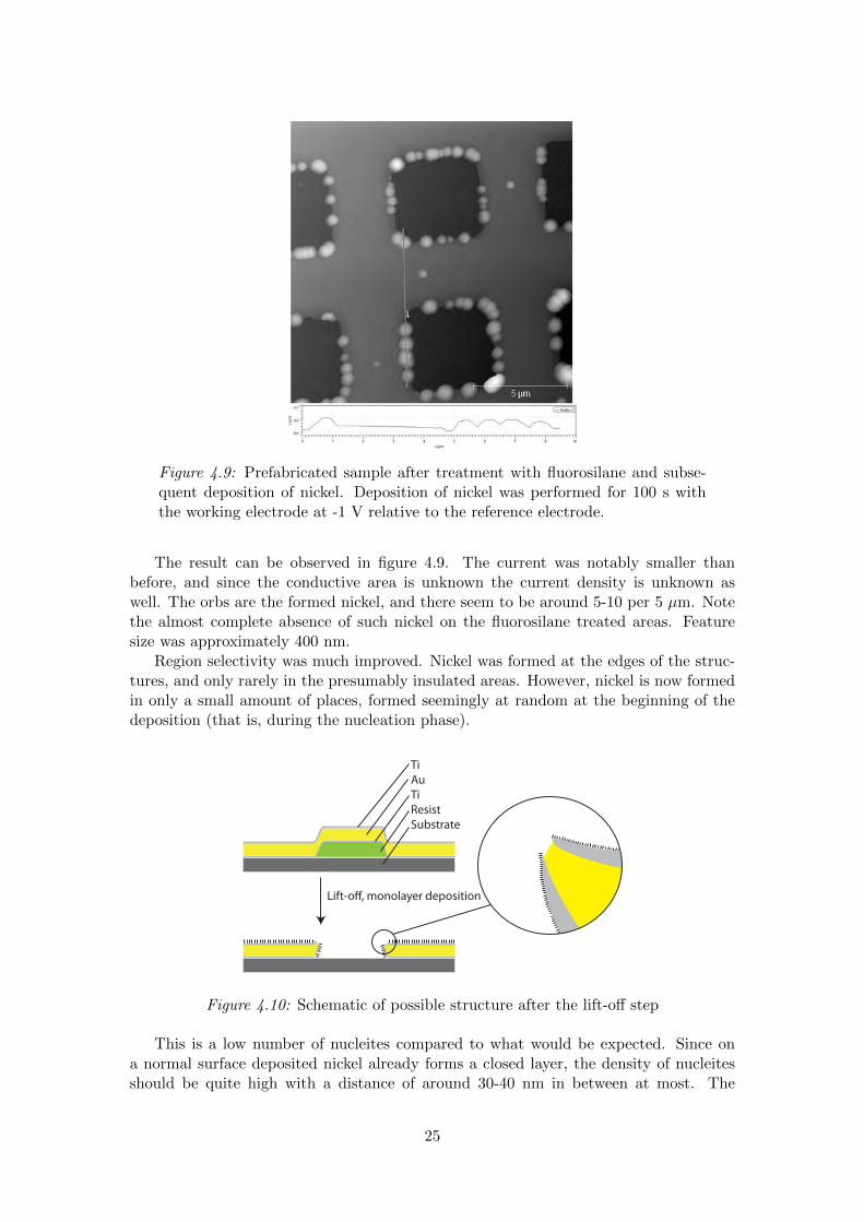
Figure 4.9: Prefabricated sample after treatment with fluorosilane and subse-quent deposition of nickel. Deposition of nickel was performed for 100 s withthe working electrode at -1 V relative to the reference electrode.
The result can be observed in figure 4.9. The current was notably smaller thanbefore, and since the conductive area is unknown the current density is unknown aswell. The orbs are the formed nickel, and there seem to be around 5-10 per 5 �m. Notethe almost complete absence of such nickel on the fluorosilane treated areas. Featuresize was approximately 400 nm.
Region selectivity was much improved. Nickel was formed at the edges of the struc-tures, and only rarely in the presumably insulated areas. However, nickel is now formedin only a small amount of places, formed seemingly at random at the beginning of thedeposition (that is, during the nucleation phase).
TiAuTiResistSubstrate
Lift-o�, monolayer deposition
Figure 4.10: Schematic of possible structure after the lift-off step
This is a low number of nucleites compared to what would be expected. Since ona normal surface deposited nickel already forms a closed layer, the density of nucleitesshould be quite high with a distance of around 30-40 nm in between at most. The
25
thickness of the gold layer is 100 nm, which means forming a continuous line shouldreally not be an issue.
One explanation for this is depicted in figure 4.10. It is possible that the sidewalls ofthe lift-off structures were also mostly covered by titanium. Titanium has a high tensilestrength, so it is not unlikely to stretch during the lift-off process before tearing.
In such areas, the fluoride monolayer would also be deposited - this would inhibitthe deposition of nickel. A solution for this problem would be to avoid lift-off and use adifferent method (such as etching) to pattern the substrate.
4.3.3 Influence of voltage on nickel nucleation
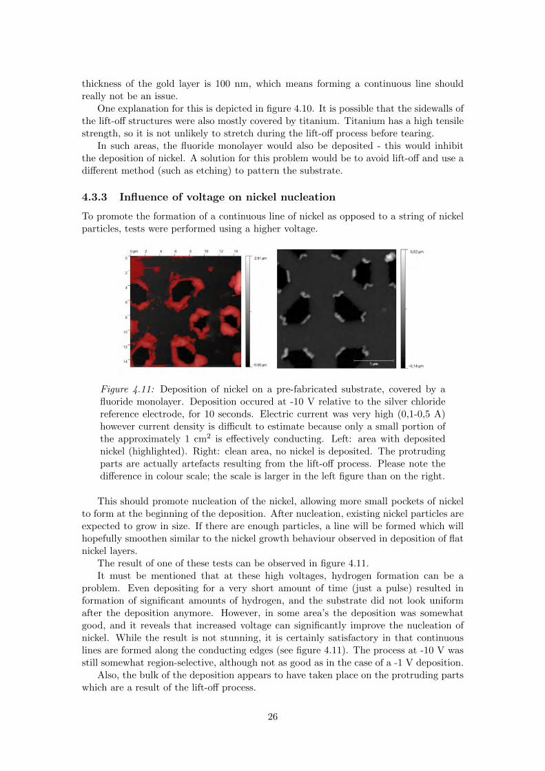
To promote the formation of a continuous line of nickel as opposed to a string of nickelparticles, tests were performed using a higher voltage.
Figure 4.11: Deposition of nickel on a pre-fabricated substrate, covered by afluoride monolayer. Deposition occured at -10 V relative to the silver chloridereference electrode, for 10 seconds. Electric current was very high (0,1-0,5 A)however current density is difficult to estimate because only a small portion ofthe approximately 1 cm2 is effectively conducting. Left: area with depositednickel (highlighted). Right: clean area, no nickel is deposited. The protrudingparts are actually artefacts resulting from the lift-off process. Please note thedifference in colour scale; the scale is larger in the left figure than on the right.
This should promote nucleation of the nickel, allowing more small pockets of nickelto form at the beginning of the deposition. After nucleation, existing nickel particles areexpected to grow in size. If there are enough particles, a line will be formed which willhopefully smoothen similar to the nickel growth behaviour observed in deposition of flatnickel layers.
The result of one of these tests can be observed in figure 4.11.It must be mentioned that at these high voltages, hydrogen formation can be a
problem. Even depositing for a very short amount of time (just a pulse) resulted information of significant amounts of hydrogen, and the substrate did not look uniformafter the deposition anymore. However, in some area’s the deposition was somewhatgood, and it reveals that increased voltage can significantly improve the nucleation ofnickel. While the result is not stunning, it is certainly satisfactory in that continuouslines are formed along the conducting edges (see figure 4.11). The process at -10 V wasstill somewhat region-selective, although not as good as in the case of a -1 V deposition.
Also, the bulk of the deposition appears to have taken place on the protruding partswhich are a result of the lift-off process.
26
4.3.4 Influence of nickel ion concentration on nucleation
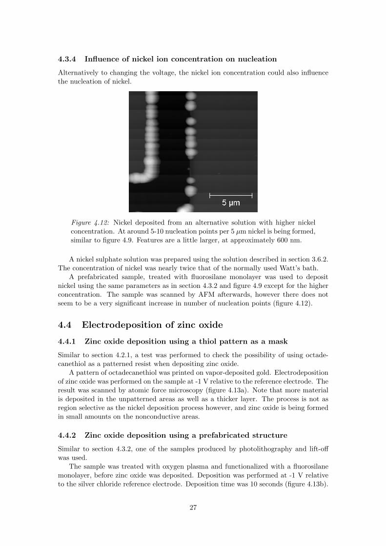
Alternatively to changing the voltage, the nickel ion concentration could also influencethe nucleation of nickel.
Figure 4.12: Nickel deposited from an alternative solution with higher nickelconcentration. At around 5-10 nucleation points per 5 �m nickel is being formed,similar to figure 4.9. Features are a little larger, at approximately 600 nm.
A nickel sulphate solution was prepared using the solution described in section 3.6.2.The concentration of nickel was nearly twice that of the normally used Watt’s bath.
A prefabricated sample, treated with fluorosilane monolayer was used to depositnickel using the same parameters as in section 4.3.2 and figure 4.9 except for the higherconcentration. The sample was scanned by AFM afterwards, however there does notseem to be a very significant increase in number of nucleation points (figure 4.12).
4.4 Electrodeposition of zinc oxide
4.4.1 Zinc oxide deposition using a thiol pattern as a mask
Similar to section 4.2.1, a test was performed to check the possibility of using octade-canethiol as a patterned resist when depositing zinc oxide.
A pattern of octadecanethiol was printed on vapor-deposited gold. Electrodepositionof zinc oxide was performed on the sample at -1 V relative to the reference electrode. Theresult was scanned by atomic force microscopy (figure 4.13a). Note that more materialis deposited in the unpatterned areas as well as a thicker layer. The process is not asregion selective as the nickel deposition process however, and zinc oxide is being formedin small amounts on the nonconductive areas.
4.4.2 Zinc oxide deposition using a prefabricated structure
Similar to section 4.3.2, one of the samples produced by photolithography and lift-offwas used.
The sample was treated with oxygen plasma and functionalized with a fluorosilanemonolayer, before zinc oxide was deposited. Deposition was performed at -1 V relativeto the silver chloride reference electrode. Deposition time was 10 seconds (figure 4.13b).
27
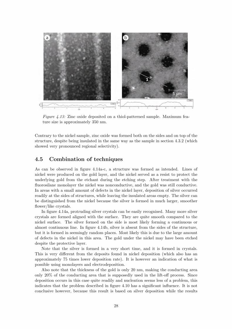
Figure 4.13: Zinc oxide deposited on a thiol-patterned sample. Maximum fea-ture size is approximately 350 nm.
Contrary to the nickel sample, zinc oxide was formed both on the sides and on top of thestructure, despite being insulated in the same way as the sample in section 4.3.2 (whichshowed very pronounced regional selectivity).
4.5 Combination of techniques
As can be observed in figure 4.14a-c, a structure was formed as intended. Lines ofnickel were produced on the gold layer, and the nickel served as a resist to protect theunderlying gold from the etchant during the etching step. After treatment with thefluorosilane monolayer the nickel was nonconductive, and the gold was still conductive.In areas with a small amount of defects in the nickel layer, deposition of silver occurredreadily at the sides of structures, while leaving the insulated areas empty. The silver canbe distinguished from the nickel because the silver is formed in much larger, smootherflower/like crystals.
In figure 4.14a, protruding silver crystals can be easily recognised. Many more silvercrystals are formed aligned with the surface. They are quite smooth compared to thenickel surface. The silver formed on the side is most likely forming a continuous oralmost continuous line. In figure 4.14b, silver is absent from the sides of the structure,but it is formed in seemingly random places. Most likely this is due to the large amountof defects in the nickel in this area. The gold under the nickel may have been etcheddespite the protective layer.
Note that the silver is formed in a very short time, and it is formed in crystals.This is very different from the deposits found in nickel deposition (which also has anapproximately 75 times lower deposition rate). It is however an indication of what ispossible using monolayers and electrodeposition.
Also note that the thickness of the gold is only 20 nm, making the conducting areaonly 20% of the conducting area that is supposedly used in the lift-off process. Sincedeposition occurs in this case quite readily and nucleation seems less of a problem, thisindicates that the problem described in figure 4.10 has a significant influence. It is notconclusive however, because this result is based on silver deposition while the results
28
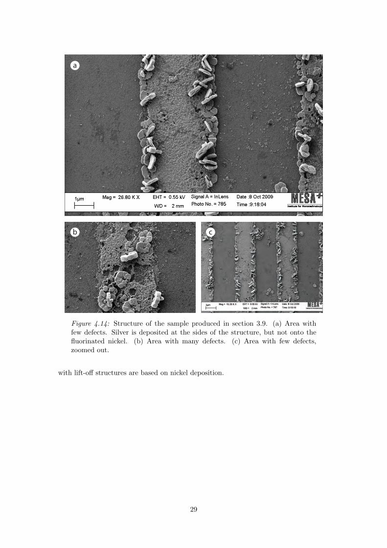
cb
a
Figure 4.14: Structure of the sample produced in section 3.9. (a) Area withfew defects. Silver is deposited at the sides of the structure, but not onto thefluorinated nickel. (b) Area with many defects. (c) Area with few defects,zoomed out.
with lift-off structures are based on nickel deposition.
29
Chapter 5
Conclusion and recommendations
5.1 Monolayer as an etch resist
The realization of gold patterns by etching proved difficult with the materials used in thisresearch. Patterns of gold were realized, but during the etching process the monolayeris definitely not stable.
In this research, the quality of the gold layer was improved. Tests indicate that thisis a significant factor in the stability of the alkanethiol on the gold, as better resultswere obtained using flatter and less porous gold samples. However, there are also otherfactors influencing the effectiveness of the monolayer etch resists.
An important factor is the permeability of the monolayer combined with the natureof the etchant. The permeability of the monolayer may have been too high in case ofthe iodide based etch resist. This could be influenced by several factors.
Between the monolayer deposition and the etching step, alcohol was used to removeexcess alkanethiol. This may have had the side effect of mixing some alcohol into themonolayer, which would increase the affinity of the monolayer for polar and ionic agents- increasing the permeability. If this is a factor, it is possible to remove such tracecs ofalcohol by exposing the sample to a vacuum for a short time and/or heating it.
While in this research only one etchant was used, different etchants are available.Successes have been reported using cyanide-based etching solutions, and another optionis the use of polymer based complexing agents. If the complexing agent is polymer basedthe permeability of the monolayer will be negligible. In such a situation, the monolayerwould likely remain intact and could even be used again in later stages of a fabricationprocess.
It would be recommendable for future research to improve on this step by changingthe etchant, possibly testing a polymer-based complexing agent, as well as by usingevaporation to deposit the substrates.
5.2 Monolayer as an electrodeposition mask
It appears that a pattern of an octadecanethiol monolayer can effectively prevent theformation of nickel. This is likely to work for similarly deposited metals as well, such ascopper. The perfluoride monolayer also effectively prevents the nickel from depositing.This is also likely to work for similarly deposited metals.
However, the zinc oxide is not as regio-selective as nickel. In the alkanethiol case,there was selectivity - but the selectivity was not good enough. In the perfluoride case,the zinc oxide appeared to grow preferentially on the monolayer. This suggest that the
30
type of surface is of major influence, and the choice of which monolayer is used is ofmajor influence. It may be possible to improve on this process by growing more slowlyafter nucleation, or by using a different monolayer. Since many factors are of influenceon the zinc oxide deposition, other factors may contribute as well.
Note that relative conduction of the areas is much more of a factor on the directdeposition of metals such as nickel, than it is in the case of zinc oxide. This is becausethe zinc oxide is not directly deposited. Hydroxide ions are formed directly on thesurface, and such ions form a complex with nickel. This complex forms nucleites of zincdihydroxide, preferably on a surface which has some affinity to zinc dihydroxide, andfinally decomposes and forms solid zinc oxide. It may also decompose before finding thesurface, which means that the surface needs to have affinity for zinc oxide.
In either case, the surface properties are of major influence. To ensure that zincoxide is deposited in the right areas and not in the wrong areas, the right areas musthave a higher affinity for either zinc dihydroxide, zinc oxide, or both (depending on theactual mechanism, which may also depend on factors like temperature). The conductingproperties are, especially at a smaller scale, less influential.
5.3 Deposition on the side of structures
Structures with nickel deposited only on the side-walls were realized as was intended.However, there are several challenges which must be met if this technique is to be usedin a fabrication process.
The most important challenge is the formation of a continuous line of nickel at asmaller scale. To achieve this, the number of nucleites must be increased. Tests haveindicated that the applied potential has a significant effect on the nucleation of nickel,while the concentration of nickel ions in the solution is less influential.
Another factor which may have been of influence is the way the structures werefabricated (see section 4.3.2). To examine whether or not this is a factor, similar testscould be performed with samples prepared by for example photolithography combinedwith etching (instead of photolithography and lift-off).
One test (see section 4.5) was performed with a sample produced without a lift-offstep. The thickness of the gold layer was only 20 nm (as opposed to 100), and thematerial deposited on the sides was silver. The results were quite promising, and it isrecommendable to perform tests on similar structures using other metals such as copper.Copper deposition should be a straightforward step using a solution of copper sulphateand sulphuric acid. Note however that this is primarily for experimental purposes, sincecopper can diffuse into the gold and form an undesired allow if in direct contact.
Structures with zinc oxide on the side-walls have proven more difficult to realize.Since the deposition is not a direct deposition, the conduction of a surface is less of anissue than the affinity of such a surface for the deposited material. It may be possible toform zinc oxide only on the sidewalls of a structure, however to realize this it is importantto control the factors involved in zinc oxide deposition as well as possible.
An easier route to the realization of zinc oxide lines on a surface is by using a template.Doing so would likely allow for the formation of zinc oxide lines with small feature sizes,similar to the result produced by Chenxiang Xiang et al [20]. It may be necessary toreduce the current density to ensure that the process is not diffusion-limited.
31
Bibliography
[1] Michael B. Cortie. The weird world of nanoscale gold. Gold Bulletin, 37:12–19,2004.
[2] George M. Whitesides et al. James L. Wilbur. Microcontact printing of self-assembled monolayers: applications in microfabrication. Nanotechnology, 7:452–457, 1996.
[3] Younan Xia and George M. Whitesides. Soft lithography. Angewandte Chemie int.ed., 37:550–575, 1998.
[4] Matthias Geissler and Younan Xia. Patterning: principles and some new develop-ments. Advanced Materials, 16:1249–1269, 2004.
[5] Arjen P. Quist et al. Recent advances in microcontact printing. Analytical andbioanalytical chemistry, 381:591–600, 2005.
[6] Frank Schreiber. Structure and growth of self-assembling monolayers. Progress inSurface Science, 65:151–256, 2000.
[7] B. Viaris de Lesegno C. ODwyer, * G. Gay and J. Weiner. The nature of alka-nethiol self-assembled monolayer adsorption on sputtered gold substrates. Lang-muir, 20:8172–8182, 2004.
[8] Abraham Ulman. Formation and structure of self-assembled monolayers. ChemicalReviews, 96:1533–1554, 1996.
[9] Hiroyuki Sugimara et al. Photolithography based on organosilane self-assembledmonolayer resist. Electrochimica Acta, 47:103–107, 2001.
[10] C. O’Dwyer. In situ examination of the selective etching of an alkanethiol monolayercovered au{111} surface. Materials letters, 61:3837–3841, 2007.
[11] Jiunn-Der Liao et al. Yi-Te Wu. Microcontact printing pattern as a mask forchemical etching: A scanning photoelectron microscopy study. The Journal ofVacuum Science and Technology B, 25(5):1729–1736, 2007.
[12] B. Michel M. Geissler, H. Schmid and E. Delamarche. Selective wet-etching ofmicrocontact-printed cu substrates with control over the etch profile. Microelec-tronic Engineering, 6768:326332, 2003.
[13] Kirt R. Williams. Etch rates for micromachining processing, part ii. Journal ofmicroelectromechanical systems, 12:761–778, 2003.
[14] Eddy Rodijk. Zinc oxide nanowires: Synthesis and Characterization. Master’sthesis, University of Twente, the Netherlands, February 2009.
32
[15] M. E. Sibert and M. A. Steinberg. Electrodeposition of titanium on base metals.Journal of the electrochemical society, 102:641–647, 1955.
[16] Kathleen J. Stebe Noshir S. Pesika, A. Radisic and Peter C. Searson. Fabrica-tion of complex architectures using electrodeposition into patterned self-assembledmonolayers. Nanoletters, 6:1023–1026, 2006.
[17] Christophe Leger et al. Growth patterns in electrodeposition. Physica A, 263:305–314, 1999.
[18] A. Dumont P. vanden Brande and Rene Winand. Nucleation and growth of nickelby electrodeposition under galvanostatic circumstances. Journal of applied electro-chemistry, 24:201–205, 1994.
[19] Chengxiang Xiang et al. Lithographically patterned nanowire electrodeposition. phys. stat. sol. (c), 5:35033505, 2008.
[20] Chenxiang Xiang et al. Lithographically patterned nanowire electrodeposition: Amethod for patterning electrically continuous metal nanowires on dielectrics. Amer-ican Chemical Society, 2:1939–1949, 2008.
[21] C. Madore and D Landolt. Blocking inhibitors in cathodic leveling. The Electro-chemical Society, 143:3936–3943, 1996.
[22] John O Dukovic and Charles W. Tobias. Simulation of leveling in electrodeposition.The Electrochemical Society, 137:3748–3755, 1990.
[23] Sophie Peulon and Daniel Lincot. Mechanistic study of cathodic elecfrodepositionof zinc oxide and zinc hydroxychioride films from oxygenated aqueous zinc chloridesolutions. The Electrochemical Society, 145:864–874, 1998.
33


![2 LASER INTERFERENCE LITHOGRAPHY - uni-halle.de · 2 LASER INTERFERENCE LITHOGRAPHY (LIL) 9 2 LASER INTERFERENCE LITHOGRAPHY (LIL) Laser interference lithography [3~22] (LIL) is a](https://img.pdfslide.net/doc/110x75/5eae180eecc7e273a41a4e88/2-laser-interference-lithography-uni-hallede-2-laser-interference-lithography.jpg)