Embed Size (px)
Citation preview
commodoresemiconductor group
MOS TECHNOLOGY, INC.950 Rittenhouse Rd., Norristown, PA 19403 ■ Tel.: 215/666-7950 - TLX 846-100 MOSTECHGY VAFG
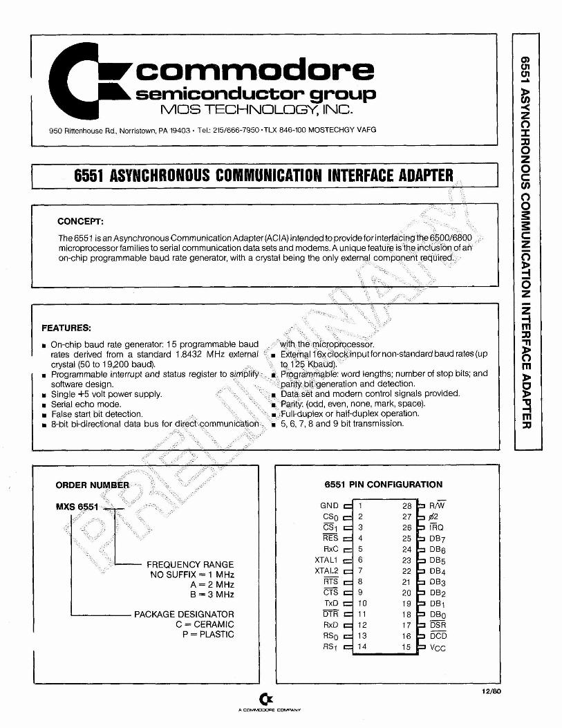
6551 ASYNCHRONOUS COMMUNICATION INTERFACE ADAPTER
CONCEPT: %
The 6551 is an Asynchronous Communication Adapter (ACIA) intended to provide for interfacing the 6500/6800 microprocessor families to serial communication data sets and modems. A unique feature is the inclusion of an on-chip programmable baud rate generator, with a crystal being the only external component required.
FEATURES:
■ On-chip baud rate generator: 15 programmable baud rates derived from a standard 1.8432 MHz external crystal (50 to 19,200 baud).
■ Programmable interrupt and status register to simplify software design.
■ Single +5 volt power supply.■ Serial echo mode,■ False start bit detection.■ 8-bit bi-directional data bus for direct communication
with the microprocessor.External 16x clock input for non-standard baud rates (up to 125 Kbaud).Programmable: word lengths; number of stop bits; and parity bit generation and detection.Data set and modern control signals provided.Parity: (odd, even, none, mark, space).Full-duplex or half-duplex operation.5, 6, 7, 8 and 9 bit transmission.
ORDER NUMBER
MXS6551 -
— FREQUENCY RANGE NO SUFFIX = 1 MHz
A = 2 MHz B = 3 MHz
PACKAGE DESIGNATOR C = CERAMIC
P = PLASTIC
6551 PIN CONFIGURATION
G N D n= 1 28 3 R/WC S 0 c= 2 27 3 ^ 2CS-| cr 3 26 3 IRQRES t= 4 25 3 D B 7
RxC i— 5 24 3 D B 6
XTAL1 x=. 6 23 3 D B 5
XTAL2 i= 7 22 3 D B 4
RTS i= 8 2 1 3 D B 3
CTS t= 9 20 3 D B 2
TxD c = 1 0 19 3 DB-idTr t= 11 18 3 DBoRxD c= 12 17 3 DSRRSo t= 13 16 3 DCDR S t r= 14 15 =» vCc
c *A CO M M O O O PE C O M PA N Y
12/80
6551 ASYNCHRO
NOUS
CO
MM
UNIC
ATION
INTERFACE AD
APTER
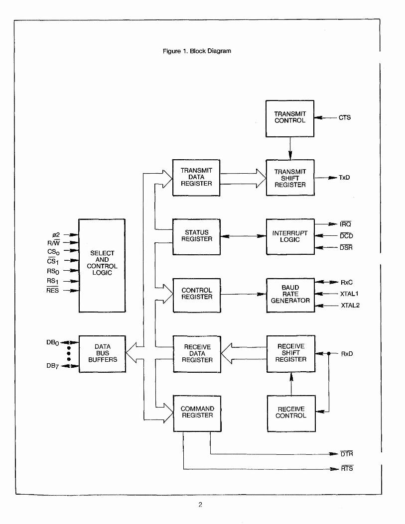
Figure 1. Block Diagram
TRANSMITCONTROL CTS
02 -» *■R/W —»►cs0 SELECTCSi -» *■ AND
CONTROLRSo — ► LOGICRSiRES —* ►
^ • DATA• BUS• BUFFERS
d b 7 - »
TRANSMITDATA
REGISTER -Nn /
'TRANSMIT
SHIFTREGISTER
•TxD
STATUSREGISTER
CONTROLREGISTER
BAUDRATE
GENERATOR
RECEIVEDATA
REGISTER
RxC
XTAL1
XTAL2
RECEIVESHIFT
REGISTER
COMMAND RECEIVEREGISTER CONTROL
RxD
- DTR
RTS
2
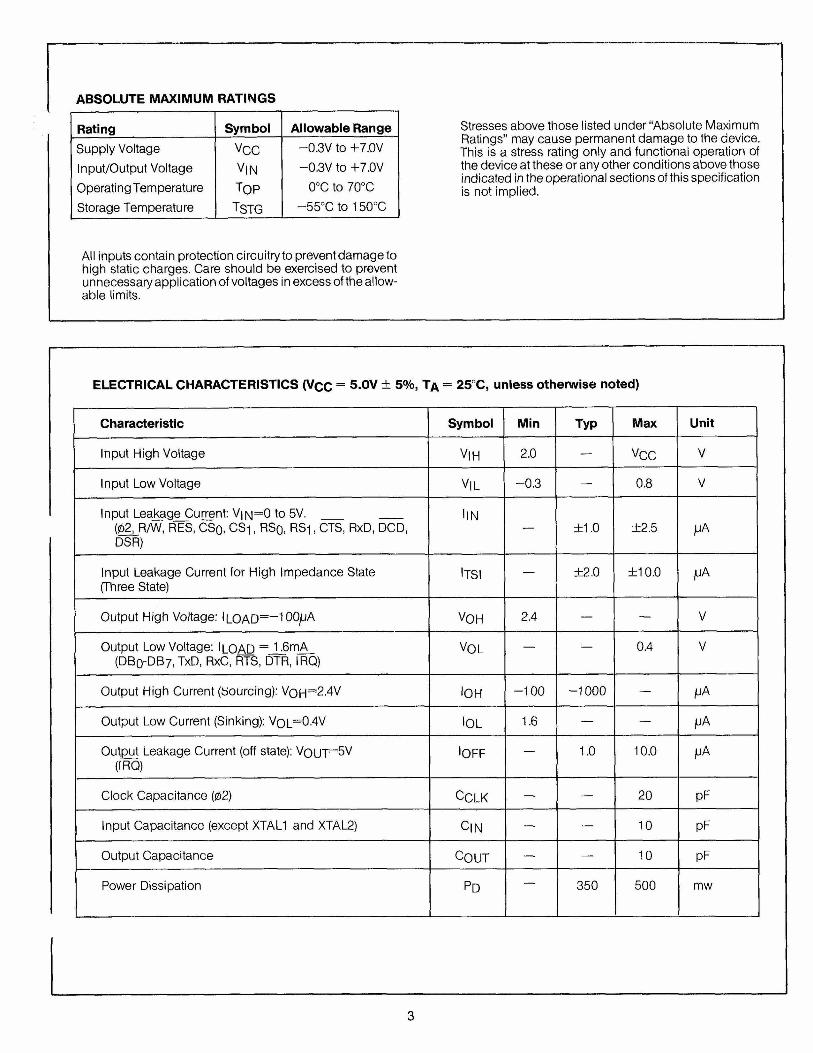
ABSOLUTE MAXIMUM RATINGS
Rating Symbol Allowable Range
Supply Voltage Input/Output Voltage Operating Temperature Storage Temperature
VccV|Nto p
tstg
-0.3V to +7.0V -0.3V to +7.0V
0°C to 70°C —55°C to 150°C
Stresses above those listed under “Absolute Maximum Ratings” may cause permanent damage to the device. This is a stress rating only and functional operation of the device at these or any other conditions above those indicated in the operational sections of this specification is not implied.
All inputs contain protection circuitryto prevent damage to high static charges. Care should be exercised to prevent unnecessary application of voltages in excess of the allowable limits.
ELECTRICAL CHARACTERISTICS (Vq c = 5.0V ± 5%, Ta = 25°C, unless otherwise noted)
Characteristic Symbol Min Typ Max Unit
Input High Voltage V|H 2.0 — Vcc V
Input Low Voltage V|L -0 .3 — 0.8 V
Input Leakage Current: V|n = 0 to 5V.(02, R/W, RES, CSo, C S i, RSo, R S i, CTS, RxD, DCD, DSR)
IlN— ± 1.0 ±2.5 jj A
Input Leakage Current for High Impedance State (Three State)
ITSI — ± 2.0 ± 10.0 juA
Output High Voltage: IlOAD= - 1 OOjjA VOH 2.4 — — V
Output Low Voltage: I LOAD = 1 -6mA (DB0-DB7, TxD, RxC, RTS, DTR, IRQ)
VOL — — 0.4 V
Output High Current (aourcing): Vo h =2.4V lOH -100 -1000 — MA
Output Low Current (Sinking): Vo l=0.4V lOL 1.6 — — juA
Output Leakage Current (off state): Vo u t= 5V (IRQ)
lOFF — 1.0 10.0 PA
Clock Capacitance (02) CCLK — — 20 pF
Input Capacitance (except XTAL1 and XTAL2) C|N — — 10 PF
Output Capacitance COUT — — 10 PF
Power Dissipation PD — 350 500 mw
3
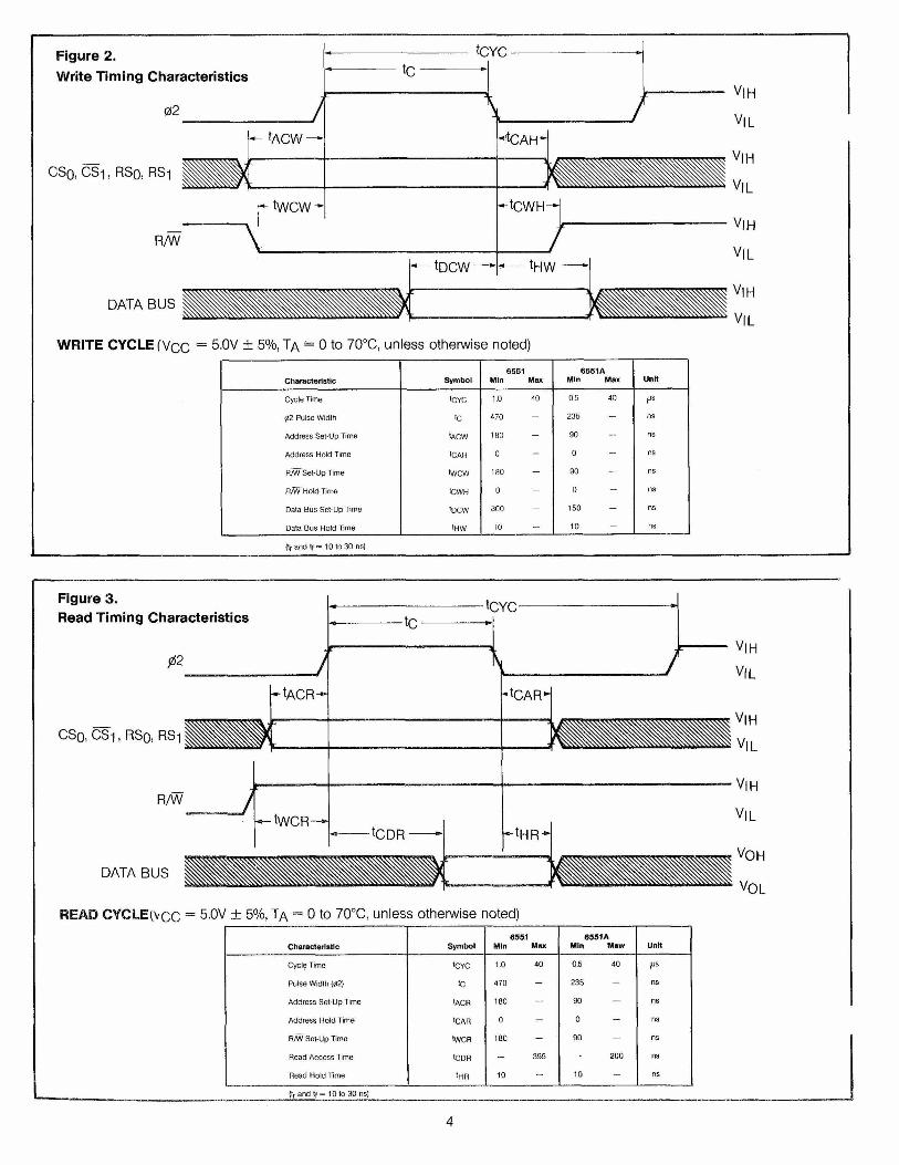
Characteristic Symbol6551
Min Max6551A
Min Max Unit
Cycle Time tCYC 1.0 40 0.5 40 ps
02 Pulse Width tc 470 - 235 - ns
Address Set-Up Time tACW 180 - 90 - ns
Address Hold Time tCAH 0 - 0 ns
R/W Set-Up Time tw cw 180 - 90 - ns
R/WHoldTime tCWH 0 _ 0 - ns
Data Bus Set-Up Time tDCW 300 - 150 - ns
Data Bus Hold Time tHW 10 - 10 - ns
(Ir and tf = 10 to 30 ns)
Figure 3.Read T im ing Characteristics
CS0, CS-I, RSo, RS1
DATA BUS
R/W
READ CYCLE(vqc = 5.0V ± 5%, Ta = 0 to 70°C, unless otherwise noted)
Characteristic Symbol0551
Min Max0551A
Min Maw Unit
Cycle Time tCYC 1.0 40 0.5 40 fjs
Pulse Width {02) tc 470 - 235 - ns
Address Set-Up Time tACR 180 “ 90 - ns
Address Hold Time tCAR 0 0 ~ ns
R/W Set-Up Time tWCR 180 - 90 - ns
Read Access Time tCDR 395 200 ns
Read Hold Time tHR 10 “ 10 ns
(tr and tf = 10 to 30 ns)
4
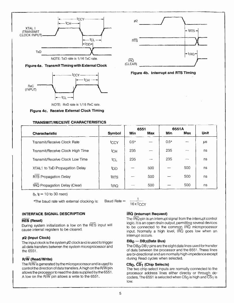
- tC H -XTAL1
(TRANSMIT CLOCK IN PU T). I
-tC C Y
\ /- tC L -
'tDD>
TxD XNOTE: TxD rate is 1 /16 TxC rate.
Figure 4a. Transm it T im ing w ith External Clock
RxC(INPUT)
NOTE: RxD rate is 1 /16 RxC rate.
Figure 4c. Receive External C lock Tim ing
TRANSMIT/RECEIVE CHARACTERISTICS
Characteristic Symbol6551
Min Max6551A
Min Max Unit
Transmit/Receive Clock Rate tCCY 0.5* — 0.5* — jUS
Transmit/Receive Clock High Time tCH 235 — 235 — ns
Transmit/Receive Clock Low Time tCL 235 — 235 — ns
XTAL1 to TxD Propagation Delay tDD — 500 — 500 ns
RTS Propagation Delay tRTS — 500 — 500 ns
IRQ Propagation Delay (Clear) t|RQ — 500 — 500 ns
(tr, tf = 10 to 30 nsec)
*The baud rate with external clocking is: Baud Rate : 116xTcCY
INTERFACE SIGNAL DESCRIPTION
RES (Reset) ___During system initialization a low on the RES input will cause internal registers to be cleared.
02 (Input Clock)The input clock is the system 02 clock and is used to trigger all data transfers between the system microprocessor and the 6551.
R/W (Read/Write)The R/W is generated by the microprocessorand is used to control the direction of data transfers. A high on the R/W pin allows the processor to read the data supplied by the 6551. A low on the R/W pin allows a write to the 6551.
IRQ (interrupt Request)The IRQ pin is an interrupt signal from the interrupt control logic. It is an open drain output, permitting several devices to be connected to the common IRQ microprocessor input. Normally a high level, IRQ goes low when an interrupt occurs.DBo — DB7 (Data Bus)The DB0-DB7 pins are the eight data lines used fortransfer of data between the processor and the 6551. These lines are bi-directional and are normally high-impedance except during Read cycles when selected.
CSo> CS1 (Chip Selects)The two chip select inputs are normally connected to the processor address lines either directly or through de- coders.The 6551 is selected when CSo is high and CS1 is low.
5
RSo, RS-f (Register Selects)
The two register select lines are normally connected to the processor address lines to allow the processor to select the various 6551 internal registers. The following table indicates the internal register select coding:
RSi RS0 Write Read
0 0 Transmit Data Register
Receiver Data Register
0 1 Programmed Reset (Data is “Don’t Care”)
Status Register
1 0 Command Register1 1 Control Register
The table shows that only the Command and Control registers are read/write. The Programmed Reset operation does not cause any data transfer, but is used to clear the 6551 registers. The Programmed Reset is slightly different from the Hardware Reset (RES) and these differences are described in the individual register definitions.
ACIA/MODEM INTERFACE SIGNAL DESCRIPTION
XTAL1, XTAL2 (Crystal Pins)These pins are normally directly connected to the external crystal (1.8432 M Hz) used to derive the various baud rates. Alternatively, an externally generated clock may be used to drive the XTAL1 pin, in which case the XTAL2 pin must float. XTAL1 is the input pin for the transmit clock.
TxD (Transmit Data)The TxD output line is used to transfer serial NRZ (non- return-to-zero) data to the modem. The LSB (least significant bit) of the Transmit Data Register is the first data bit transmitted and the rate of data transmission is determined by the baud rate selected.
RxD (Receive Data)The RxD input line is used to transfer serial N RZ data into the ACIA from the modem, LSB first. The receiver data rate is either the programmed baud rate or the rate of an externally generated receiver clock. This selection is made by programming the Control Register.
RxC (Receive Clock)
The RxC is a bi-directional pin which serves as either the receiver 16x clock input or the receiver 16x clock output. The latter mode results if the internal baud rate generator is selected for receiver data clocking.
RTS (Request to Send)
The RTS outpin pin is used to control the modem from the processor. The state of the RTS pin is determined by the contents of the Command Register.
CTS (Clear to Send)The CTS input pin is used to control the transmitter operation. The enable state is with CTS low. The transmitter is automatically disabled if CTS is high.
DTR (Data Terminal Ready)This ouput pin is used to indicate the status of the 6551 to the modem. A low on DTR indicates the 6551 is enabled and a high indicates it is disabled. The processor controls this pin via bit 0 of the Command Register.
DSR (Data Set Ready)The DSR input pin is used to indicate to the 6551 the status of the modem. A low indicates the “ready” state and a high, “not-ready”.
DCD (Data Carrier Detect)The DCD input pin is used to indicate to the 6551 the status of the carrier-detect output of the modem. A low indicates that the modern carrier signal is present and a high, that it is not.
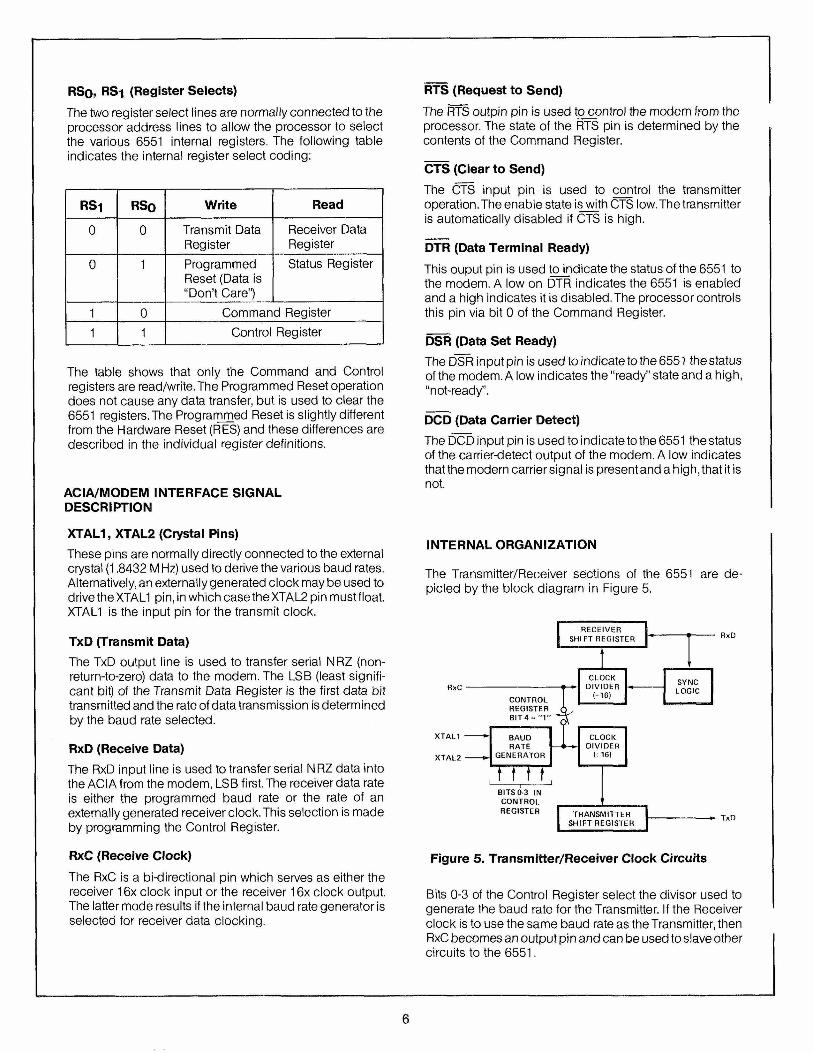
INTERNAL ORGANIZATION
The Transmitter/Receiver sections of the 6551 are depicted by the block diagram in Figure 5.
Figure 5. Transm itter/Receiver C lock Circuits
Bits 0-3 of the Control Register select the divisor used to generate the baud rate for the Transmitter. If the Receiver clock is to use the same baud rate as the Transmitter, then RxC becomes an output pin and can be used to slave other circuits to the 6551.
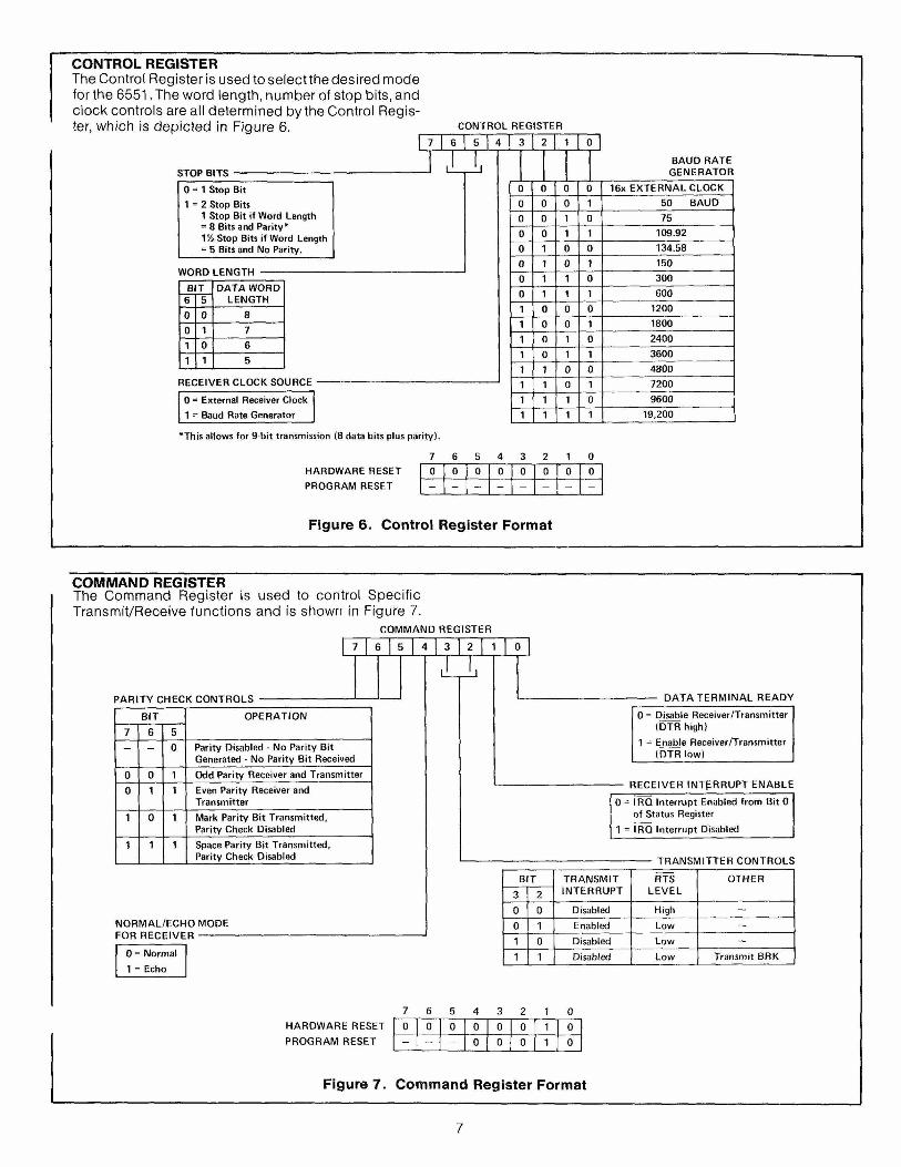
CONTROL REGISTERThe Control Register is used to select the desired mode for the 6551. The word length, number of stop bits, and clock controls are all determined by the Control Register, which is depicted in Figure 6.
STOP BITS
CONTROL REGISTER | 5 l 4 l 3 l 2 | l | o ]
0 = 1 Stop Bit 1 = 2 Stop Bits
1 Stop Bit if Word Length = 8 Bits and Parity*V/z Stop Bits if Word Length = 5 Bits and No Parity.
WORD LENGTHBIT DATA WORD
LENGTH6 50 0 80 1 71 0 61 1 5
RECEIVER CLOCK SOURCE
0 = External Receiver Clock1 - Baud Rate Generator
HARDWARE RESET PROGRAM RESET
*This allows for 9-bit transmission (8 data bits plus parity).
7 6
BAUD RATE GENERATOR
0 0 0 0 16x EXTERNAL CLOCK0 0 0 1 50 BAUD0 0 1 0 750 0 1 1 109.920 1 0 0 134.580 1 0 1 1500 1 1 0 3000 1 1 1 6001 0 0 0 12001 0 0 1 18001 0 1 0 24001 0 1 1 36001 1 0 0 48001 1 0 1 72001 1 1 0 96001 1 1 1 19,200
0 0 0 0 0 0 0 0
Figure 6. C ontro l Register Format
COMMAND REGISTERThe Command Register is used to control Specific Transmit/Receive functions and is shown in Figure 7.
COMMAND REGISTER
7 6 5 4 3 2 1 0
PARITY CHECK CONTROLS
BIT OPERATION7 6 5
- - 0 Parity Disabled • No Parity Bit Generated ■ No Parity Bit Received
0 0 1 Odd Parity Receiver and Transmitter0 1 1 Even Parity Receiver and
Transmitter1 0 1 Mark Parity B it Transmitted,
Parity Check Disabled1 1 1 Space Parity Bit Transmitted,
Parity Check Disabled
NORMAL/ECHO MODE FOR RECEIVER -----------
0 = Normal1 = Echo
DATA TERMINAL READY
0 = Disable Receiver/Transmitter{DTR high)
1 = Enable Receiver/Transmitter{DTR low)
RECEIVER INTERRUPT ENABLE
0 = IRQ Interrupt Enabled from Bit 0of Status Register
1 = IRQ Interrupt Disabled
TRANSMITTER CONTROLS
BIT TRANSMITINTERRUPT
RTSLEVEL
OTHER3 20 0 Disabled High -0 1 Enabled Low -1 0 Disabled Low -1 1 Disabled Low Transmit BRK
1 0HARDWARE RESET 0 0 0 0 0 0 1 0PROGRAM RESET - „ - 0 0 0 1 0
Figure 7. Command Register Form at
7
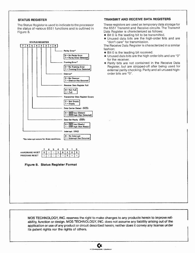
STATUS REGISTER TRANSMIT AND RECEIVE DATA REGISTERS
The Status Register is used to indicate to the processor the status of various 6551 functions and is outlined in Figure 8.
STATUS REGISTER
i l t°~i| L— —— Parity Error*
0 = No Parity Error1 = Parity Error Detected
Framing Error*
0 = No Framing Error1 = Framing Error Detected
Overrun*
These registers are used as temporary data storage for the 6551 Transmit and Receive circuits. The Transmit Data Register is characterized as follows:© Bit 0 is the leading bit to be transmitted,® Unused data bits are the high-order bits and are
“don’t care” for transmission.The Receive Data Register is characterized in a similar fashion:© Bit 0 is the leading bit received.® Unused data bits are the high-order bits and are “0”
for the receiver.® Parity bits are not contained in the Receive Data
Register, but are stripped-off after being used for external parity checking. Parity and all unused high- order bits are “0” .
0 = No Overrun1 = Overrun Has Occurred
Receiver Data Register Full
0 = Not Full1 = Full
Transmitter Data Register Empty
0 - Not Empty1 = Empty
Data Carrier Detect (DCD)
0 = DCD low (Detect)1 = DCD high (Not Detected)
Data Set Ready (DSR)
0 - DSR low (Ready)1 “ DSR high (Not Ready)
*No interrupt occurs for these conditions.
Interrupt (IRQ)
0 = No Interrupt1 = Interrupt Has Occurred
7 6 5 4 3 2 1 0HARDWARE RESET 0 - - 1 0 0 0 0PROGRAM RESET - - - - _ 0 - -
Figure 8. S tatus R egister Form at
MOS TECHNOLOGY, INC. reserves the right to make changes to any products herein to improve reliability, function or design. MOS TECHNOLOGY, INC. does not assume any liability arising out of the application or use of any product or circuit described herein; neither does it convey any license under its patent rights nor the rights of others.
A COM MOOOOC C O M PA N Y