Embed Size (px)
Citation preview
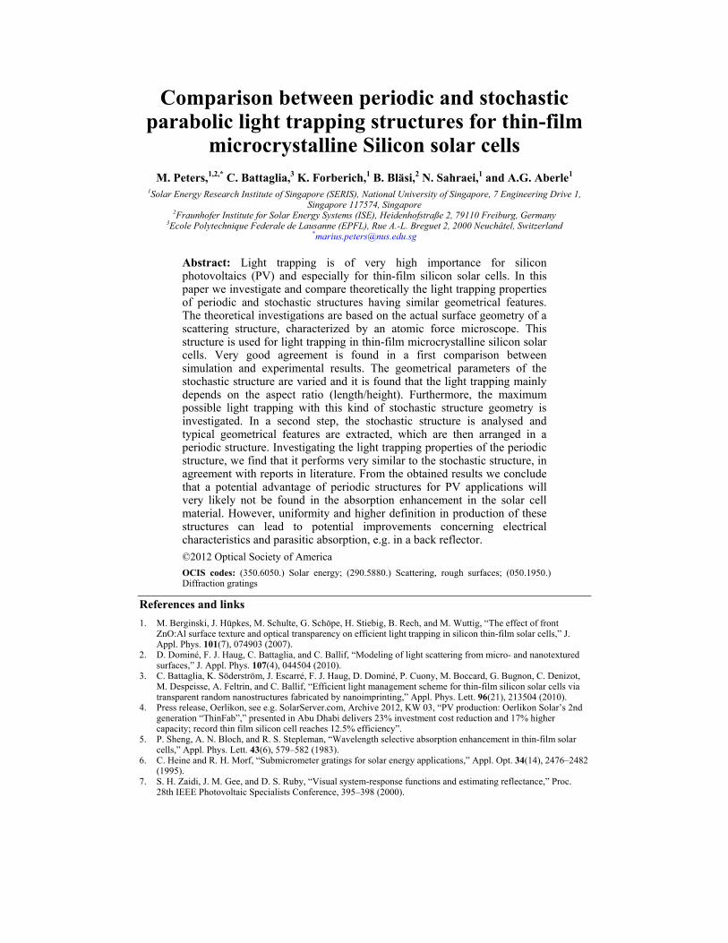
Comparison between periodic and stochastic parabolic light trapping structures for thin-film
microcrystalline Silicon solar cells M. Peters,1,2,* C. Battaglia,3 K. Forberich,1 B. Bläsi,2 N. Sahraei,1 and A.G. Aberle1
1Solar Energy Research Institute of Singapore (SERIS), National University of Singapore, 7 Engineering Drive 1, Singapore 117574, Singapore
2Fraunhofer Institute for Solar Energy Systems (ISE), Heidenhofstraße 2, 79110 Freiburg, Germany 3Ecole Polytechnique Federale de Lausanne (EPFL), Rue A.-L. Breguet 2, 2000 Neuchâtel, Switzerland
Abstract: Light trapping is of very high importance for silicon photovoltaics (PV) and especially for thin-film silicon solar cells. In this paper we investigate and compare theoretically the light trapping properties of periodic and stochastic structures having similar geometrical features. The theoretical investigations are based on the actual surface geometry of a scattering structure, characterized by an atomic force microscope. This structure is used for light trapping in thin-film microcrystalline silicon solar cells. Very good agreement is found in a first comparison between simulation and experimental results. The geometrical parameters of the stochastic structure are varied and it is found that the light trapping mainly depends on the aspect ratio (length/height). Furthermore, the maximum possible light trapping with this kind of stochastic structure geometry is investigated. In a second step, the stochastic structure is analysed and typical geometrical features are extracted, which are then arranged in a periodic structure. Investigating the light trapping properties of the periodic structure, we find that it performs very similar to the stochastic structure, in agreement with reports in literature. From the obtained results we conclude that a potential advantage of periodic structures for PV applications will very likely not be found in the absorption enhancement in the solar cell material. However, uniformity and higher definition in production of these structures can lead to potential improvements concerning electrical characteristics and parasitic absorption, e.g. in a back reflector.
©2012 Optical Society of America
OCIS codes: (350.6050.) Solar energy; (290.5880.) Scattering, rough surfaces; (050.1950.) Diffraction gratings
References and links
1. M. Berginski, J. Hüpkes, M. Schulte, G. Schöpe, H. Stiebig, B. Rech, and M. Wuttig, “The effect of front ZnO:Al surface texture and optical transparency on efficient light trapping in silicon thin-film solar cells,” J. Appl. Phys. 101(7), 074903 (2007).
2. D. Dominé, F. J. Haug, C. Battaglia, and C. Ballif, “Modeling of light scattering from micro- and nanotextured surfaces,” J. Appl. Phys. 107(4), 044504 (2010).
3. C. Battaglia, K. Söderström, J. Escarré, F. J. Haug, D. Dominé, P. Cuony, M. Boccard, G. Bugnon, C. Denizot, M. Despeisse, A. Feltrin, and C. Ballif, “Efficient light management scheme for thin-film silicon solar cells via transparent random nanostructures fabricated by nanoimprinting,” Appl. Phys. Lett. 96(21), 213504 (2010).
4. Press release, Oerlikon, see e.g. SolarServer.com, Archive 2012, KW 03, “PV production: Oerlikon Solar’s 2nd generation “ThinFab”,” presented in Abu Dhabi delivers 23% investment cost reduction and 17% higher capacity; record thin film silicon cell reaches 12.5% efficiency”.
5. P. Sheng, A. N. Bloch, and R. S. Stepleman, “Wavelength selective absorption enhancement in thin-film solar cells,” Appl. Phys. Lett. 43(6), 579–582 (1983).
6. C. Heine and R. H. Morf, “Submicrometer gratings for solar energy applications,” Appl. Opt. 34(14), 2476–2482 (1995).
7. S. H. Zaidi, J. M. Gee, and D. S. Ruby, “Visual system-response functions and estimating reflectance,” Proc. 28th IEEE Photovoltaic Specialists Conference, 395–398 (2000).
8. M. Peters, M. Rüdiger, H. Hauser, M. Hermle, and B. Bläsi, “Diffractive gratings for crystalline silicon solar cells - optimum parameters and loss mechanisms,” Prog. Photovolt. Res. Appl. 20(7), 862–873 (2012).
9. A. Mellor, I. Tobias, A. Marti, M. J. Mendes, and A. Luque, “Upper limits to absorption enhancement in thick solar cells using diffraction gratings,” Prog. Photovolt. Res. Appl. 19(6), 676–687 (2011).
10. Z. Yu, A. Raman, and S. Fan, “Fundamental limit of light trapping in grating structures,” Opt. Express 18(S3), A366–A380 (2010).
11. J. Gjessing, A. S. Sudbo, and E. S. Marstein, “A novel back-side light trapping structure for thin silicon solar cells,” J. Euro. Opt. Soc. 6, 11020 1–4 (2011).
12. C. van Trigt, “Visual system-response functions and estimating reflectance,” J. Opt. Soc. Am. A 14(4), 741–755 (1997).
13. E. Yablonovitch, “Statistical Ray Optics,” J. Opt. Soc. Am. A 72(7), 899–907 (1982). 14. T. Kirchartz in, “Physics of nanostructured solar cells,” V. Badescu (Edt.), Nova Science Publishers, 1–40 (2009) 15. H. Li, R. Franken, R. L. Stolk, J. K. Rath, and R. E. I. Schropp, “Mechanism of shunting of nanocrystalline
silicon solar cells deposited on rough Ag/ZnO substrates,” So. State. Phen. 131–133, 27–32 (2007). 16. M. Peters, B. Bläsi, S. W. Glunz, A. G. Aberle, J. Luther, and C. Battaglia, “Optical Simulation of Silicon Thin-
Film Solar Cells,” En. Proc. 15, 212–219 (2012). 17. V. E. Ferry, M. A. Verschuuren, M. C. Lare, R. E. I. Schropp, H. A. Atwater, and A. Polman, “Optimized Spatial
Correlations for Broadband Light Trapping Nanopatterns in High Efficiency Ultrathin Film a-Si:H Solar Cells,” Nano Lett. 11(10), 4239–4245 (2011).
18. B. Bläsi, H. Hauser, and A. J. Wolf, “Photon management structures for solar cells,” proceedings of SPIE 8438, Photonics for Solar Energy Systems IV, 84380F (2012), doi:10.1117/12.921824.
19. M. Peters, K. Forberich, C. Battaglia, A. G. Aberle, and B. Bläsi, “Comparison of periodic and random structures for scattering in thin-film microcrystalline silicon solar cells,” proceedings of SPIE 8438, Photonics for Solar Energy Systems IV, 84380F (2012), doi:10.1117/12.921774.
20. K. Jäger, R. A. C. M. M. van Swaaij, and M. Zeman, “A Full Scalar Scattering Model for Nano-Textured Interfaces”, in “Optical Nanostructures and Advanced Materials for Photovoltaics,” proceedings of the Optical Society of America, PWC5 (2011).
21. B. Vet, B. Grancic, O. Isabella, S. Solntsev, and M. Zeman, “Optical and Electrical Simulations of Advanced Silicon Based Solar Cell Devices,” Proceedings of the 24th European Photovoltaic Solar Energy Conference 2682–2685 (2009).
22. M. G. Moharam, D. A. Pommet, E. B. Grann, and T. K. Gaylord, “Stable implementation of the rigorous coupled-wave analysis for surface-relief gratings: enhanced transmittance matrix approach,” J. Opt. Soc. Am. A 12(5), 1077–1086 (1995).
23. P. Lalanne and M. P. Jurek, “Computation of the near-field pattern with the coupled wave method for transverse magnetic polarization,” J. Mod. Opt. 45(7), 1357–1374 (1998).
24. International Electrotechnical Standard, (IEC 60904–1), www.iec.ch. 25. H. E. A. Elgamel, “High efficiency polycrystalline silicon solar cells using low temperature PECVD process,”
IEEE Trans. Electron. Dev. 45, 2131–2137 (1998). 26. A. V. Shah, H. Schade, M. Vanecek, J. Meier, E. Vallat-Sauvain, N. Wyrsch, U. Krol, C. Droz, and J. Bailat,
“Thin-film Silicon Solar Cell Technology,” Prog. Photovolt. Res. Appl. 12(23), 113–142 (2004). 27. A. V. Shah, ed., “Thin-film Silicon Solar Cell Cells,” EPFL Press 1st edition, 216 - 231 (2010). 28. C. Battaglia, J. Escarre, K. Soederstroem, M. Boccard, and C. Ballif, “Experimental Evaluation of the Light
Trapping Potential of Optical Nanostructures for Thin-Film Silicon Solar Cells,” En. Proc. 15, 206–211 (2012). 29. S. Fahr, T. Kirchartz, C. Rockstuhl, and F. Lederer, “Approaching the Lambertian limit in randomly textured
thin-film solar cells,” Opt. Express 19(S4 Suppl 4), A865–A874 (2011). 30. D. Domine, “The role of front electrodes and intermediate reflectors in the optoelectronic properties of high
efficiency micromorph solar cells,” PhD Thesis, University of Neuchatel (2009). 31. C. Battaglia, C. M. Hsu, K. Söderström, J. Escarré, F. J. Haug, M. Charrière, M. Boccard, M. Despeisse, D. T. L.
Alexander, M. Cantoni, Y. Cui, and C. Ballif, “Light Trapping in Solar Cells: Can Periodic Beat Random?” ACS Nano 6(3), 2790–2797 (2012).
1. Introduction
Light trapping is of key importance for the further development of thin-film silicon photovoltaics (PV). A widely used and efficient approach to realize light trapping in thin-film silicon solar cells is to apply scattering textures at the interface between the transparent front electrode and the silicon layers. These textures are typically stochastically modulated transparent conductive oxide (TCO) surfaces onto which the photoactive silicon layers are deposited. A typical process to realize such textured TCO surfaces is by etching of sputtered ZnO layers [1]. The effectiveness of scattering textures has been shown by various authors [2,3] and the current world record for thin-film silicon solar cells has been achieved with a sophisticated hierarchical random texture [4].
Another promising approach is light trapping with diffractive, periodic structures like 1D or 2D gratings or photonic crystals. This concept was first proposed by Sheng et al. [5] for binary linear gratings for thin-film silicon solar cells. Later this concept was investigated for
other types of solar cells and other grating geometries [6–8]. Experimentally, considerable absorption enhancements could be achieved; however, the performance of gratings has not yet surpassed that of scattering textures.
A general question is whether periodic or random structures are more advantageous for light trapping. It is generally agreed that diffraction has a higher potential for enhancing the internal path length of light inside a solar cell [9]. Scattering structures, on the other hand are well established, have achieved good results in the lab and in mass-scale manufacturing, and are less expensive to fabricate. In this paper, we discuss a comparison between periodic and random structures with a similar geometry. For a fair comparison between the periodic and random structures we consider two very important points:
1. The investigated structures should have realistic geometries. Very good light trapping properties were shown theoretically for periodic structures [10,11], but an open question for these structures is still whether they can be produced at acceptable cost.
2. The periodic and random structures should be of geometrical similarity. What we mean by this, the problems connected with this issue, and how we define a similar geometry is discussed in detail in the next section.
Following that, we give a short introduction into the simulation methods used in this paper. Based on the structures defined in the preceding section, we show a theoretical analysis of their light trapping properties and how they change if the geometry of the structure is varied. A comparison between the properties of periodic and random structures is given. First, we compare the measured random structure to the constructed periodic structure with the initial parameter set. The comparison is then extended towards optimized parameters. For the random structures, an analysis of the light trapping potential for a certain solar cell geometry is also given and a light trapping limit is defined. The paper concludes with a summary of the most important results.
2. Structure definition
One problem every comparison between periodic and stochastic structures has to face is the choice of exactly which structures to compare. A first step towards a comparison is to look at the potential absorption enhancement factor in the limit of low absorption for both light trapping mechanisms. For diffractive gratings, Kirchartz has calculated a thermodynamic limit of 893n [12] with n the refractive index of the absorber material, resulting in a value of about 3000 for crystalline silicon. This number is, however, based on highly idealised assumptions and experimentally reported absorption enhancement factors are much lower. For scattering, a factor of 4n2 (approximately 50 for crystalline silicon) as calculated by Yablonovitch [13, 14] is often referred to as a limit. The value of 4n2 is obtained for a Lambertian light distribution inside the absorber layer. However, scattering characteristics can be constructed that result in higher absorption enhancements. In practice the Lambertian “limit” has proven to be useful (though, strictly speaking, it is only a limit if the incident light is completely diffuse). In actual solar cells, the absorption enhancement factor due to scattering structures is well below that of a Lambertian scatterer. In a later section we will have a further look into the absorption limit of scattering structures.
A second path to follow would be to compare ideal stochastic and periodic structures. However, as a Lambertian scatterer seems to be a good choice for an ideal scattering structure, it is unclear how an ideal periodic structure looks like. The light trapping properties of periodic structures depend largely on their shape. Examples for very efficient periodic structures with quite sophisticated shapes are given in literature [10,11] but no method is known yet to construct an ideal structure . This problem aggravates for periodic and stochastic structures if the electrical properties of solar cells are taken into account. Too high a surface roughness will result in shunting [14] of the cell, severely reducing its efficiency. An optically very good structure is then electrically detrimental, and vice versa.
Given this situation, we have chosen another path. Our analysis is based on an existing texture that has been used to fabricate efficient thin-film silicon solar cells. An atomic force
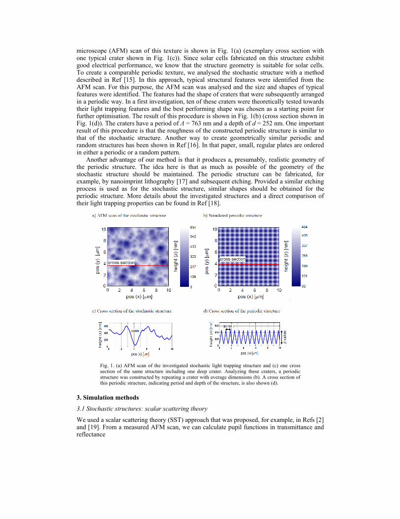
microscope (AFM) scan of this texture is shown in Fig. 1(a) (exemplary cross section with one typical crater shown in Fig. 1(c)). Since solar cells fabricated on this structure exhibit good electrical performance, we know that the structure geometry is suitable for solar cells. To create a comparable periodic texture, we analysed the stochastic structure with a method described in Ref [15]. In this approach, typical structural features were identified from the AFM scan. For this purpose, the AFM scan was analysed and the size and shapes of typical features were identified. The features had the shape of craters that were subsequently arranged in a periodic way. In a first investigation, ten of these craters were theoretically tested towards their light trapping features and the best performing shape was chosen as a starting point for further optimisation. The result of this procedure is shown in Fig. 1(b) (cross section shown in Fig. 1(d)). The craters have a period of Λ = 763 nm and a depth of d = 252 nm. One important result of this procedure is that the roughness of the constructed periodic structure is similar to that of the stochastic structure. Another way to create geometrically similar periodic and random structures has been shown in Ref [16]. In that paper, small, regular plates are ordered in either a periodic or a random pattern.
Another advantage of our method is that it produces a, presumably, realistic geometry of the periodic structure. The idea here is that as much as possible of the geometry of the stochastic structure should be maintained. The periodic structure can be fabricated, for example, by nanoimprint lithography [17] and subsequent etching. Provided a similar etching process is used as for the stochastic structure, similar shapes should be obtained for the periodic structure. More details about the investigated structures and a direct comparison of their light trapping properties can be found in Ref [18].
Fig. 1. (a) AFM scan of the investigated stochastic light trapping structure and (c) one cross section of the same structure including one deep crater. Analyzing these craters, a periodic structure was constructed by repeating a crater with average dimensions (b). A cross section of this periodic structure, indicating period and depth of the structure, is also shown (d).
3. Simulation methods
3.1 Stochastic structures: scalar scattering theory
We used a scalar scattering theory (SST) approach that was proposed, for example, in Refs [2] and [19]. From a measured AFM scan, we can calculate pupil functions in transmittance and reflectance
0 1 0 1 2( , )2 ( , )( )i x y n i x y n nR TG e and G eκ ζ κ ζ −= = (1)
In these equations R and T denote reflection and transmission, κ0 is the vacuum wave vector of the incident light, n1 and n2 are the refractive indices of incident and outgoing medium and ζ(x,y) is the measured height of the scattering surface. The angular distribution of reflected and transmitted light is obtained from the Fourier transform of the respective pupil function. Haze values are calculated by
2 22 2 14 4 (
1 1rms rmsn n n
R TH e and H eπσ πσ
λ λ− − −
= − = − (2) with σrms the rms roughness as determined from the AFM scan and λ the wavelength of
incident light. Subsequently, haze and angular distribution function are used as input parameters for the ASA opto-electrical device simulator [20] to calculate the absorbance in the silicon layer.
3.2 Periodic structures: rigorous coupled wave analysis (RCWA)
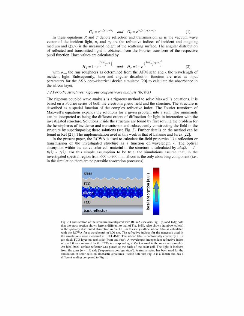
The rigorous coupled wave analysis is a rigorous method to solve Maxwell’s equations. It is based on a Fourier series of both the electromagnetic field and the structure. The structure is described as a spatial function of the complex refractive index. The Fourier transform of Maxwell’s equations expands the solutions for a given problem into a sum. The summands can be interpreted as being the different orders of diffraction for light in interaction with the investigated structure. Solutions inside the structure are found by first solving the problem for the hemispheres of incidence and transmission and subsequently constructing the field in the structure by superimposing these solutions (see Fig. 2). Further details on the method can be found in Ref [21]. The implementation used in this work is that of Lalanne and Jurek [22].
In the present paper, the RCWA is used to calculate far-field properties like reflection or transmission of the investigated structure as a function of wavelength λ. The optical absorption within the active solar cell material in the structure is calculated by abs(λ) = 1 - R(λ) - T(λ). For this simple assumption to be true, the simulations assume that, in the investigated spectral region from 600 to 900 nm, silicon is the only absorbing component (i.e., in the simulation there are no parasitic absorption processes).
Fig. 2. Cross section of the structure investigated with RCWA (see also Fig. 1(b) and 1(d); note that the cross section shown here is different to that of Fig. 1(d)). Also shown (rainbow colors) is the spatially distributed absorption in the 1.1 μm thick crystalline silicon film as calculated with the RCWA for a wavelength of 800 nm. The refractive indices for the materials used in the simulations were measured at EPFL-IMT. The silicon film is conformally coated by a 1.8 μm thick TCO layer on each side (front and rear). A wavelength-independent refractive index of n = 2.0 was assumed for the TCOs (corresponding to ZnO as used in the measured sample). An ideal back surface reflector was placed at the back of the solar cell. The light is incident from the glass (n = 1.5) side (‘superstrate configuration’). A similar setup has been used for the simulation of solar cells on stochastic structures. Please note that Fig. 2 is a sketch and has a different scaling compared to Fig. 1.

3.2 Calculation of solar cell characteristics
A first useful quantity is the absorbed photocurrent density jph. This quantity states how much current a solar cell would produce if every absorbed photon would contribute one electron to the current generation. We use a slightly different quantity here, the constricted photocurrent density, which gives the absorbed photocurrent within a certain spectral range [λ1,λ2]
2
1 21
, , ( ) ( )phj e d absλ
λ λ λλ λ φ λ= (3)
In this equation e is the elementary charge and φ(λ) is the spectral flux density of sunlight. In this work we used the AM1.5G solar spectrum as defined in Ref [23]. For several reasons, jph constitutes an upper limit for the current that a conventional solar cell can generate within the considered wavelength range. First, not all absorption occurring in a solar cell contributes to current generation. Parts of the light can, for example, be absorbed in the antireflection coating or in the (metal) reflector. In a strict treatment, useful and parasitic absorption need to be distinguished. Furthermore, electronic loss mechanisms (recombination) are not considered here. Some of these losses are of a fundamental nature.
A quantity summarising all losses (electronic and optical due to parasitic absorption) in the solar cell is the internal quantum efficiency IQE. IQE and short-circuit current density jSC of a solar cell can then be related by
( ) ( ) ( )SCj e d IQE absλ λ λ φ λ= (4)
Equation (4) can be used as one possible definition of the internal quantum efficiency. It must be noted, though, that the distinction between useful and parasitic absorption processes is non-trivial and to some extent arbitrary. For microcrystalline thin-film silicon solar cells, the IQE includes mainly losses due to parasitic absorption in the solar cell system.
Since in practice it is often impossible to distinguish between different loss mechanisms, and the IQE is not known exactly, it makes sense to combine the factors in Eq. (4) into another quantity, the external quantum efficiency EQE. The EQE can be defined by
( ) ( )SCj e d EQEλ λ φ λ= (5)
For the estimation of the useful absorption, we will use the EQE in this sense as a product of useful absorption and IQE. Similar to the case of a constricted photocurrent density, jSC can be defined for a certain spectral range by restricting the integral boundaries in equation.
Figure 3 shows the absorption calculated for a crystalline Si solar cell with a thickness of 1.1 μm deposited onto the texture shown in Fig. 1(a), using the SST method described in the previous section and Ref [18] and also using the simulation tool ASA [22]. Also shown is the measured EQE of the actual solar cell. Characteristics of this solar cell are given in Table 1.To compare the simulated useful absorption with the measured EQE, information about loss mechanisms, summarised in the IQE, is required. Literature values for the IQE of microcrystalline silicon solar cells vary [24–26]. According to the available data we started with a simplified approach, assuming that the external quantum efficiency is 10% lower than the absorption. This 10% reduction is due to parasitic processes such as, mainly, parasitic absorptions and, to a small extent, an imperfect carrier collection. Furthermore we assumed this reduction to be constant over the considered wavelength range. This assumption is certainly simplified but there are some experimental indications that the wavelength dependence is at least not very strong [27]. Still, especially for very long wavelengths (for which parasitic absorption becomes more important) it can be expected that the obtained results are inaccurate.
The result of this consideration is shown in Fig. 3. The black line is the EQE calculated from the simulated absorption. It is in good agreement with the measured EQE (blue dots). Also, the simulated EQE exceeds the measured EQE at long wavelengths, as expected. In fact, the agreement is better than could be expected for this simple approach, and might be
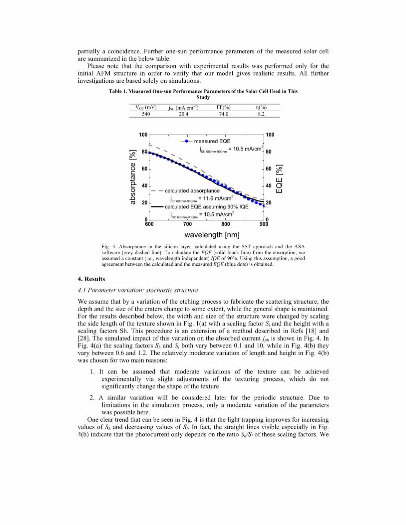
partially a coincidence. Further one-sun performance parameters of the measured solar cell are summarized in the below table.
Please note that the comparison with experimental results was performed only for the initial AFM structure in order to verify that our model gives realistic results. All further investigations are based solely on simulations.
Table 1. Measured One-sun Performance Parameters of the Solar Cell Used in This Study
VOC (mV) jSC (mA cm−2) FF(%) η(%)540 20.4 74.0 8.2
600 700 800 9000
20
40
60
80
100 measured EQE
jSC 600nm-900nm = 10.5 mA/cm2
EQ
E [%
]
calculated absorptancejph 600nm-900nm = 11.6 mA/cm2
calculated EQE assuming 90% IQEjSC 600nm-900nm = 10.5 mA/cm2
ab
sorp
tanc
e [%
]
wavelength [nm]
0
20
40
60
80
100
Fig. 3. Absorptance in the silicon layer, calculated using the SST approach and the ASA software (grey dashed line). To calculate the EQE (solid black line) from the absorption, we assumed a constant (i.e., wavelength independent) IQE of 90%. Using this assumption, a good agreement between the calculated and the measured EQE (blue dots) is obtained.
4. Results
4.1 Parameter variation: stochastic structure
We assume that by a variation of the etching process to fabricate the scattering structure, the depth and the size of the craters change to some extent, while the general shape is maintained. For the results described below, the width and size of the structure were changed by scaling the side length of the texture shown in Fig. 1(a) with a scaling factor Sl and the height with a scaling factors Sh. This procedure is an extension of a method described in Refs [18] and [28]. The simulated impact of this variation on the absorbed current jph is shown in Fig. 4. In Fig. 4(a) the scaling factors Sh and Sl both vary between 0.1 and 10, while in Fig. 4(b) they vary between 0.6 and 1.2. The relatively moderate variation of length and height in Fig. 4(b) was chosen for two main reasons:
1. It can be assumed that moderate variations of the texture can be achieved experimentally via slight adjustments of the texturing process, which do not significantly change the shape of the texture
2. A similar variation will be considered later for the periodic structure. Due to limitations in the simulation process, only a moderate variation of the parameters was possible here.
One clear trend that can be seen in Fig. 4 is that the light trapping improves for increasing values of Sh and decreasing values of Sl. In fact, the straight lines visible especially in Fig. 4(b) indicate that the photocurrent only depends on the ratio Sh/Sl of these scaling factors. We
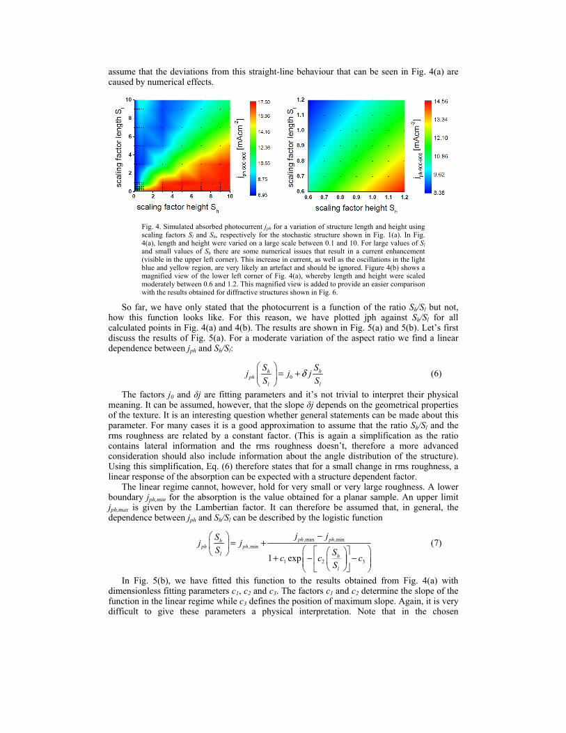
assume that the deviations from this straight-line behaviour that can be seen in Fig. 4(a) are caused by numerical effects.
Fig. 4. Simulated absorbed photocurrent jph for a variation of structure length and height using scaling factors Sl and Sh, respectively for the stochastic structure shown in Fig. 1(a). In Fig. 4(a), length and height were varied on a large scale between 0.1 and 10. For large values of Sl and small values of Sh there are some numerical issues that result in a current enhancement (visible in the upper left corner). This increase in current, as well as the oscillations in the light blue and yellow region, are very likely an artefact and should be ignored. Figure 4(b) shows a magnified view of the lower left corner of Fig. 4(a), whereby length and height were scaled moderately between 0.6 and 1.2. This magnified view is added to provide an easier comparison with the results obtained for diffractive structures shown in Fig. 6.
So far, we have only stated that the photocurrent is a function of the ratio Sh/Sl but not, how this function looks like. For this reason, we have plotted jph against Sh/Sl for all calculated points in Fig. 4(a) and 4(b). The results are shown in Fig. 5(a) and 5(b). Let’s first discuss the results of Fig. 5(a). For a moderate variation of the aspect ratio we find a linear dependence between jph and Sh/Sl:
0h h
phl l
S Sj j j
S Sδ
= +
(6)
The factors j0 and δj are fitting parameters and it’s not trivial to interpret their physical meaning. It can be assumed, however, that the slope δj depends on the geometrical properties of the texture. It is an interesting question whether general statements can be made about this parameter. For many cases it is a good approximation to assume that the ratio Sh/Sl and the rms roughness are related by a constant factor. (This is again a simplification as the ratio contains lateral information and the rms roughness doesn’t, therefore a more advanced consideration should also include information about the angle distribution of the structure). Using this simplification, Eq. (6) therefore states that for a small change in rms roughness, a linear response of the absorption can be expected with a structure dependent factor.
The linear regime cannot, however, hold for very small or very large roughness. A lower boundary jph,min for the absorption is the value obtained for a planar sample. An upper limit jph,max is given by the Lambertian factor. It can therefore be assumed that, in general, the dependence between jph and Sh/Sl can be described by the logistic function
,max ,min,min
1 2 31 exp
ph phhph ph
l h
l
j jSj j
S Sc c c
S
− = + + − −
(7)
In Fig. 5(b), we have fitted this function to the results obtained from Fig. 4(a) with dimensionless fitting parameters c1, c2 and c3. The factors c1 and c2 determine the slope of the function in the linear regime while c3 defines the position of maximum slope. Again, it is very difficult to give these parameters a physical interpretation. Note that in the chosen
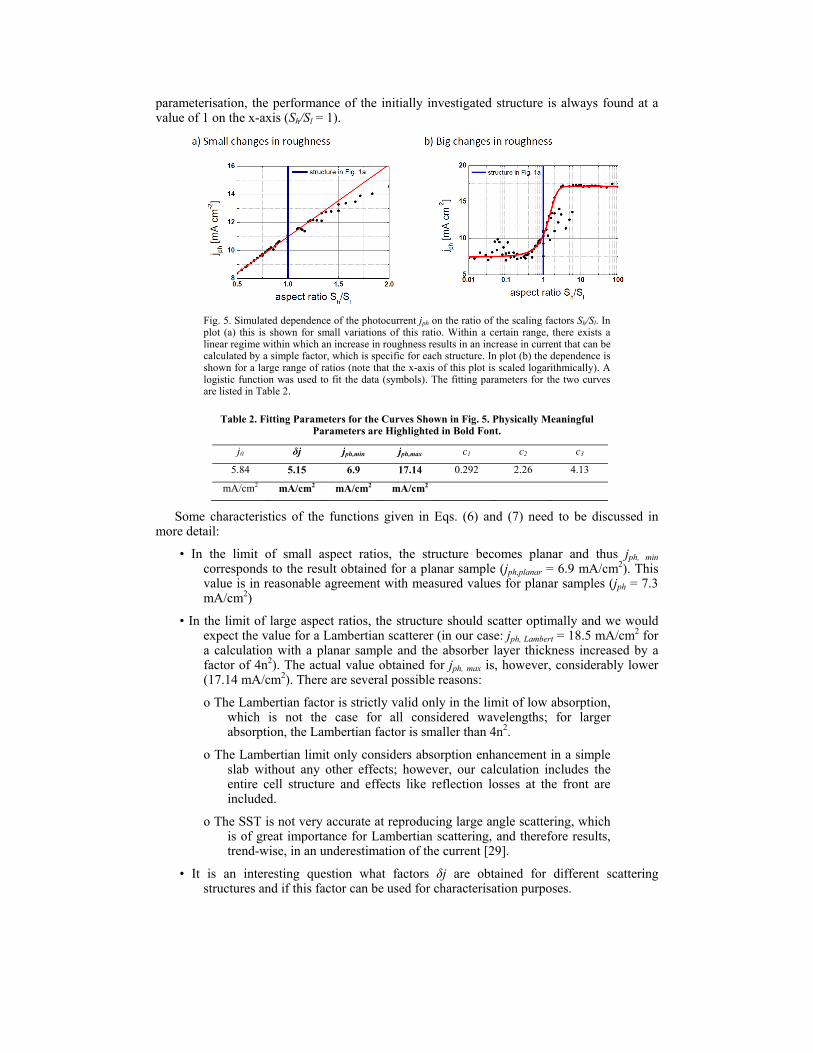
parameterisation, the performance of the initially investigated structure is always found at a value of 1 on the x-axis (Sh/Sl = 1).
Fig. 5. Simulated dependence of the photocurrent jph on the ratio of the scaling factors Sh/Sl. In plot (a) this is shown for small variations of this ratio. Within a certain range, there exists a linear regime within which an increase in roughness results in an increase in current that can be calculated by a simple factor, which is specific for each structure. In plot (b) the dependence is shown for a large range of ratios (note that the x-axis of this plot is scaled logarithmically). A logistic function was used to fit the data (symbols). The fitting parameters for the two curves are listed in Table 2.
Table 2. Fitting Parameters for the Curves Shown in Fig. 5. Physically Meaningful Parameters are Highlighted in Bold Font.
j0 δj jph,min jph,max c1 c2 c3
5.84 5.15 6.9 17.14 0.292 2.26 4.13
mA/cm2 mA/cm2 mA/cm2 mA/cm2
Some characteristics of the functions given in Eqs. (6) and (7) need to be discussed in more detail:
• In the limit of small aspect ratios, the structure becomes planar and thus jph, min corresponds to the result obtained for a planar sample (jph,planar = 6.9 mA/cm2). This value is in reasonable agreement with measured values for planar samples (jph = 7.3 mA/cm2)
• In the limit of large aspect ratios, the structure should scatter optimally and we would expect the value for a Lambertian scatterer (in our case: jph, Lambert = 18.5 mA/cm2 for a calculation with a planar sample and the absorber layer thickness increased by a factor of 4n2). The actual value obtained for jph, max is, however, considerably lower (17.14 mA/cm2). There are several possible reasons:
o The Lambertian factor is strictly valid only in the limit of low absorption, which is not the case for all considered wavelengths; for larger absorption, the Lambertian factor is smaller than 4n2.
o The Lambertian limit only considers absorption enhancement in a simple slab without any other effects; however, our calculation includes the entire cell structure and effects like reflection losses at the front are included.
o The SST is not very accurate at reproducing large angle scattering, which is of great importance for Lambertian scattering, and therefore results, trend-wise, in an underestimation of the current [29].
• It is an interesting question what factors δj are obtained for different scattering structures and if this factor can be used for characterisation purposes.
The value for jph,max obtained in this way can be interpreted as the maximum current that can be achieved with a particular solar cell architecture. The presented analysis can help to estimate how much of the light trapping potential has been realised. In the presented example, very good light trapping should be achieved if the aspect ratio is increased by a factor of three. (This is not the case for all calculated configurations, though. It is currently unclear, what causes the spreading of the data-point). This can either be done by increasing the height of the structures, or by decreasing the feature size while maintaining the height. An open question is, of course, how this can be done experimentally in a way that avoids shunting of the solar cell.
In the previously mentioned paper by Fahr et al. [28], comparable results were also shown for other textures. Those results confirm that jph,max depends on the structure geometry. Additionally it was shown that it is, in principle, possible to approach Lambertian light trapping for certain structure geometries.
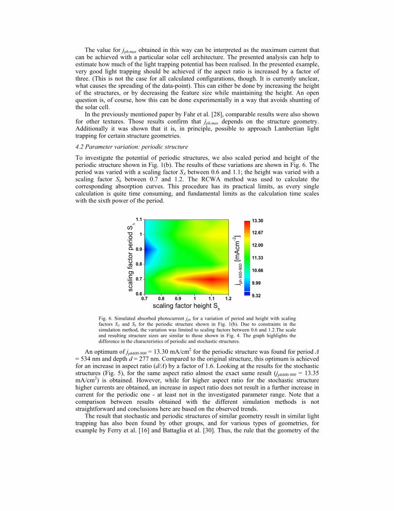
4.2 Parameter variation: periodic structure
To investigate the potential of periodic structures, we also scaled period and height of the periodic structure shown in Fig. 1(b). The results of these variations are shown in Fig. 6. The period was varied with a scaling factor SΛ between 0.6 and 1.1; the height was varied with a scaling factor Sh between 0.7 and 1.2. The RCWA method was used to calculate the corresponding absorption curves. This procedure has its practical limits, as every single calculation is quite time consuming, and fundamental limits as the calculation time scales with the sixth power of the period.
0.7 0.8 0.9 1 1.1 1.20.6
0.7
0.8
0.9
1
1.1
j ph 6
00-9
00 [m
Acm
-2]
scaling factor height Sh
scal
ing
fact
or p
erio
d S
Λ
9.32
9.99
10.66
11.33
12.00
12.67
13.30
Fig. 6. Simulated absorbed photocurrent jph for a variation of period and height with scaling factors SΛ and Sh for the periodic structure shown in Fig. 1(b). Due to constraints in the simulation method, the variation was limited to scaling factors between 0.6 and 1.2.The scale and resulting structure sizes are similar to those shown in Fig. 4. The graph highlights the difference in the characteristics of periodic and stochastic structures.
An optimum of jph600-900 = 13.30 mA/cm2 for the periodic structure was found for period Λ = 534 nm and depth d = 277 nm. Compared to the original structure, this optimum is achieved for an increase in aspect ratio (d/Λ) by a factor of 1.6. Looking at the results for the stochastic structures (Fig. 5), for the same aspect ratio almost the exact same result (jph600-900 = 13.35 mA/cm2) is obtained. However, while for higher aspect ratio for the stochastic structure higher currents are obtained, an increase in aspect ratio does not result in a further increase in current for the periodic one - at least not in the investigated parameter range. Note that a comparison between results obtained with the different simulation methods is not straightforward and conclusions here are based on the observed trends.
The result that stochastic and periodic structures of similar geometry result in similar light trapping has also been found by other groups, and for various types of geometries, for example by Ferry et al. [16] and Battaglia et al. [30]. Thus, the rule that the geometry of the
light trapping structure is more important than the question whether a structure is periodic or not, seems to be quite general. One can then further speculate that the scattering properties of a structure are mainly determined by its local features and not so much by global features. For a structure that is sufficiently homogenous, the question whether it is a good scatterer or not can then be answered by looking at its local features, like size, shape, angles and aspect ratio.
A couple of points need to be discussed about this result:
• The initial parameters were obtained from an analysis of the stochastic structure. The current that was obtained for this initial parameter set is jph = 11.5 mA/cm2. This value is almost equal to those obtained for the experiment and the initial setup of the simulated stochastic structure.
• For the periodic structure, there is no observable connection between the aspect ratio Sh/SΛ and the photocurrent. It seems rather that for certain (Sh, SΛ) combinations, minima and maxima occur for the photocurrent which can be explained by pronounced diffraction and resonance effects. The position of the maximum seems to be more sensitive to the period than to the depth.
5. Summary and discussion
In this paper, we compared and discussed light trapping properties for certain periodic and stochastic textures. The basic idea of this investigation was to look at structures with (i) a realistic geometry in the sense that they should resemble structures that can actually be produced experimentally and (ii) similar structure geometries. To achieve this, we used an AFM scan of a sputtered and etched TCO sample for the investigation of a stochastic structure. For the periodic structure, we analyzed the stochastic structure, identified typical structure feature and reconstructed craters that were then arranged in a periodic pattern. The resulting structures were subsequently analyzed theoretically and, where possible, compared to experimental results. We found:
i. The simulated external quantum efficiency, using internal quantum efficiency data from literature, for the stochastic structure is in good agreement with quantum efficiency measurements for the same sample. As a consequence, also the simulated and measured short-circuit currents are in good agreement. This result serves as a verification that the developed methods deliver realistic results.
ii. The simulated short-circuit current for the periodic and stochastic structure are almost the same.
In a second step, we varied the geometry of the periodic and random structures by scaling their length, period and height with scaling factors Sλ, SΛ and Sh, respectively. For the stochastic structure we found that:
i. The simulated current mainly depends on the Sh/Sl ratio, which basically corresponds to the aspect ratio or roughness of the structure.
ii. The generated photocurrent can be assumed to be a logistic function of the ratio Sh/Sl, with a linear response in a certain regime. The investigated structure was found to be in this linear regime, so that with an increase in aspect ratio by 10% an increase in current of approximately 0.5 mA/cm2 can be expected.
iii. The logistic function converges towards a maximum current jph,max which is specific for a certain light trapping geometry and solar cell structure. This limit can be substantially lower than the Lambertian limit as was the case for the investigated structure, though higher limits have been demonstrated by other groups.
For the periodic structure we found no dependence on the Sh/SΛ ratio, but rather specific conditions for minima and maxima in photocurrent that mainly depended on the period of the texture (as could have been expected). We furthermore found that, if optimum parameters are used for the periodic structure and if a comparable aspect ratio is used for the stochastic
structure, the result in photocurrent was still very similar. From this result we conclude that for similar geometries, periodic and random structures result in similar light trapping. This conclusion is in agreement with results reported by other groups and for other device geometries, and therefore seems to be quite general.
The results also imply that the light trapping properties of a structure seem to be related to local features. It could be interesting to investigate how local light trapping can be defined and if this can be used to create more efficient light trapping structures.
Finally, a remark concerning the question whether a stochastic or a periodic structure is more advantageous: It seems that this question will not be decided by the absorption enhancement factor that the structure induces in the active solar cell material. Potential advantages lie, however, in a greater uniformity and higher definition and precision in structure generation that can be achieved with periodic structures. A better uniformity has potential benefits for the electrical performance parameters of the solar cell, particularly the shunt resistance. Preliminary investigations indicate that, additionally, benefits can be found concerning parasitic absorption processes, for example in the back surface reflector.
Acknowledgments
The authors thank all colleagues from SERIS, Fraunhofer ISE and IMT who have contributed in one way or another to this work. SERIS is sponsored by the National University of Singapore and Singapore’s National Research Foundation (NRF) through the Singapore Economic Development Board. Parts of this work were sponsored by NRF grant NRF2009EWT-CERP001-037.