Embed Size (px)
Citation preview
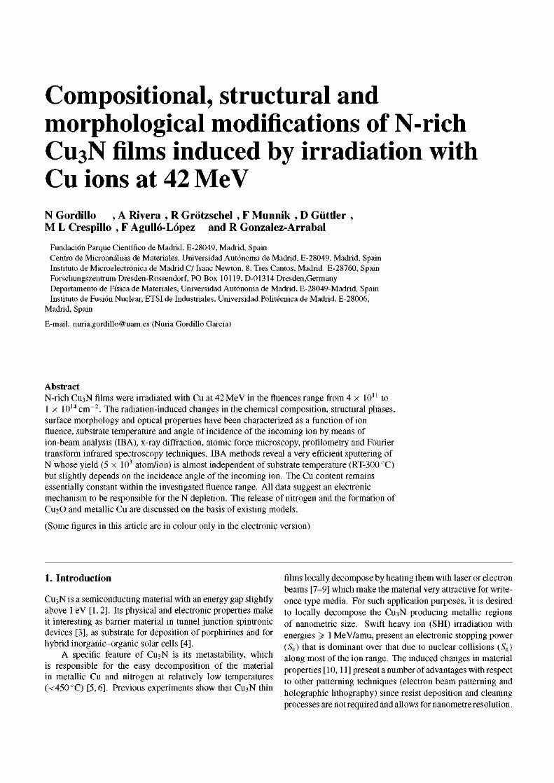
Compositional, structural and morphological modifications of N-rich C113N films induced by irradiation with Cu ions at 42 MeV N Gordillo , A Rivera , R Grótzschel , F Munnik , D Güttler , M L Crespillo , F Agulló-López and R González-Arrabal
Fundación Parque Científico de Madrid, E-28049, Madrid, Spain Centro de Microanálisis de Materiales, Universidad Autónoma de Madrid, E-28049, Madrid, Spain Instituto de Microelectrónica de Madrid C/ Isaac Newton, 8. Tres Cantos, Madrid. E-28760, Spain Forschungszentrum Dresden-Rossendorf, PO Box 10119, D-01314 Dresden,Germany Departamento de Física de Materiales, Universidad Autónoma de Madrid, E-28049-Madrid, Spain Instituto de Fusión Nuclear, ETSI de Industriales, Universidad Politécnica de Madrid, E-28006,
Madrid, Spain
E-mail: [email protected] (Nuria Gordillo García)
Abstract N-rich Q13N films were irradiated with Cu at 42 MeV in the fluences range from 4 x 10¹¹ to 1 x 10¹⁴ cirr2. The radiation-induced changes in the chemical composition, structural phases, surface morphology and optical properties have been characterized as a function of ion fluence, substrate temperature and angle of incidence of the incoming ion by means of ion-beam analysis (IBA), x-ray diffraction, atomic forcé microscopy, profilometry and Fourier transform infrared spectroscopy techniques. IBA methods reveal a very efficient sputtering of N whose yield (5 x 10³ atom/ion) is almost independent of substrate temperature (RT-300 °C) but slightly depends on the incidence angle of the incoming ion. The Cu content remains essentially constant within the investigated fluence range. All data suggest an electronic mechanism to be responsible for the N depletion. The reléase of nitrogen and the formation of Q12O and metallic Cu are discussed on the basis of existing models.
(Some figures in this article are in colour only in the electronic versión)
1. Introduction
Cu3N is a semiconducting material with an energy gap slightly above 1 eV [1,2]. Its physical and electronic properties make it interesting as barrier material in tunnel junction spintronic devices [3], as substrate for deposition of porphirines and for hybrid inorganic-organic solar cells [4].
A specific feature of Cu3N is its metastability, which is responsible for the easy decomposition of the material in metallic Cu and nitrogen at relatively low temperatures (<450°C) [5,6]. Previous experiments show that Q13N thin
films locally decompose by heating them with láser or electrón beams [7-9] which make the material very attractive for write-once type media. For such application purposes, it is desired to locally decompose the Q13N producing metallic regions of nanometric size. Swift heavy ion (SHI) irradiation with energies > 1 MeV/amu, present an electronic stopping power (Se) that is dominant over that due to nuclear collisions (Sn) along most of the ion range. The induced changes in material properties [ 10,11 ] present a number of advantages with respect to other patterning techniques (electrón beam patterning and holographic lithography) since resist deposition and cleaning processes are not required and allows for nanometre resolution.
When Se is above a certain threshold, the massive electronic excitations inside a narrow cylinder along most of the ion trajectory cause a subsequent modification of the material on a nanometre scale (ion track). The formation of nanometre metallic tracks by SHI in Cu3N may become an appropriate industrial method to fabricate advanced devices (e.g. fíat emission panels). This work is one of the first contributions to the understanding of the Cu3N decomposition upon swift-ion irradiation.
SHI irradiation has been used to genérate amorphous (latent) ion tracks in a variety of materials [12-15]. Although the track formation mechanisms are not yet fully understood, some theoretical approaches have been formulated such as the thermal spike, [16-18] the extended thermal spike [13], the excitonic [19-21] and the Coulomb explosión [22] models. At present, the thermal spike model is the most accepted one and it is commonly used to account for many features of the generated amorphous tracks, as well as the enhanced sputtering yield in the electronic stopping regime [18]. This model essentially relies on thehigh temperaturerise around the ion trajectory which causes either melting or sublimation. The subsequent fast quenching may lead to local amorphization or phase transformations. An extensión of the model [23] has been proposed to understand the creation of point defects even in the subthreshold región (i.e. before melting or boiling). The potential energy deposited as excitons in the electronic system (excitation spike) is not explicitly considered in these models as it is done in the excitonic model [19-21]. Note that for most dielectrics, the energy stored in excitons is very significant (30-50% of the total deposited energy) and according to the excitonic model, it can be used for defect generation when a non-radiative exciton decay channel may be thermally activated. In the case of SHI irradiation the thermal spike supplies the energy necessary to activate this channel. Therefore, the synergy between both the exciton and the thermal spike leads to defect generation.
Apart from the specific mechanism of the ion-solid interaction, other relevant processes must be also taken into account for a complete description of the ion-beam modification of a material: atom migration (transport processes), mainly of light species, clustering and trapping phenomena, ion-beam mixing at interfaces and sputtering. In relation to hydrides, nitrides and other volatile materials, Adel et al [24] have developed a model to describe the radiation-induced depletion of light species, which is known as the bulk molecular recombination model.
Hitherto, a few papers have been published on SHI track formation in stable metal nitride semiconductors such as GaN [25-27] and InN [28] Nevertheless, to the best of our knowledge, only one group has contributed with two papers [29,30] to the topic of SHI-induced changes in metastable Cu3N using Au at 200 MeV.
The purpose of this work is to explore the capabilities of SHIs to modify N-rich Cu3N films as a function of different parameters (fluence, substrate temperature during irradiation and angle of incidence of the incoming ion), to ascertain the role of electronic excitation and to discuss the responsible physical mechanisms in relation to existing models. To
this end, we have characterized the morphology, elemental composition and structure for films irradiated with Cu at 42 MeV using a variety of nuclear methods such as Rutherford backscattering spectrometry (RBS), nuclear reaction analysis (NRA) and elastic recoil detection analysis (ERDA). Other complementary non-nuclear techniques such as atomic forcé microscopy (AFM), profilometry, x-ray diffraction (XRD) and Fourier transform infrared spectrometry (FTIR) have also been used.
2. Experimental
Copper nitride thin films (thickness of 95 ± 5nm) were deposited at room temperature (RT) on transparent glass substrates of 1 mm thickness by de triode sputtering from a copper target in an Ar+N2 atmosphere at a de bias of -1.0 kV. More details about the deposition procedures can be found in [31].
The layers were not protected with a capping layer, but were stored in Ar atmosphere immediately after getting them out of the deposition chamber in order to prevent oxidation.
N-rich Q13N films ([N] = 33 at%) were irradiated at different temperatures (from RT to 300 °C) with a Cu beam at an energy of 42 MeV in a high vacuum chamber (pressure < 10~6 mbar) at the Forschungszentrum Rossendorf. According to SRIM calculations [32] at this beam energy the electronic stopping power (Se = 12keVnm_1) is more than two orders of magnitude higher than the nuclear stopping power (Sn = 0.07keVnm_1). Thus, the irradiation effeets are clearly dominated by the electronic processes. Several fluences in therange from4 x 10n ,upto 1 x 10¹⁴cirr2, were selected to cover the isolated as well as overlapping track regimes. The uncertainty in the fluence was less than ~10% in all cases. The current was kept low enough to avoid excessive heating of the samples.
The heating treatments during irradiation were carried out in vacuum. Subsequently, the samples remained for about 90 min in the chamber to assure cooling down to RT under vacuum conditions.
The elemental composition of the films was characterized by complementary RBS, NRA and ERDA techniques. The RBS measurements were carried out with a He+ beam at an energy of 2 MeV at the CMAM/UAM [33,34]. The backscattered He ions were collected with a commercial Si-barrier detector (ORTEC) located at 170° to the beam direction. For the NRA experiments we used the nuclear reaction [35] 14N(d,a)12C with a D+ beam at 1.8 MeV impinging onto the sample surface at normal incidence. An implanted Si detector was placed at 150° to the beam direction and operated at low bias voltage to discrimínate all protón peaks above 5 MeV. Therefore, the a0 and the a\ peaks in the spectra of the 14N (d, a)12C reaction were obtained free of background. Absolute valúes of the nitrogen área density in the films were obtained by comparison with the TiN reference sample. Since no stopper foils in front of the detector were used the Cu peak of backscattered deuterons was simultaneously measured. In order to check that the samples do not deteriórate due to the deuteron beam a sequence of four single spectra were taken at
the same spot and under the same conditions with total fluence twice as high as those used for standard analysis. No effect could be attributed to the analysing beam. ERDA was used to measure the N content during Cu irradiation. Both scattered Cu ions and recoil ions from the sample were detected at a scattering angle of 31°. The particles were measured with a Bragg ionization chamber to obtain a Z dependent signal in order to sepárate ion species. The angle between the sample normal and the incoming beam has been varied between 65° and 80°. The analysed área was about 2 x 1 mm2; the precise área was characterized after the measurement. During the measurement intermedíate files were saved to obtain the N content as a function of fluence.
Structural characterization of the Q13N films was done ex situ by /z-XRD in a Debye-Scherrer geometry using a diffractometer equipped with a GADDS bidimensional detector (Bruker-AXS, model D8 Advanced), a Culía radiation source and a collimator of 0.3 mm. The use of a /x-beam in XRD measurements allows one to focus the spot in and out of the irradiated área.
The morphology of the film surface was imaged using an atomic forcé microscope operated in the dynamic mode. A Si tip of 20 nm diameter and 60-70 kHz, special for this operation mode was used. Topography data were analysed by the free software WsxM, from Nanotec Electronics S.L. [36].
The profile across the surface of the irradiated spot was measured by a Veeco profilometer model Dtak-6M.
The optical properties of the films were characterized using aFourier transform IR spectrophotometer (FT-IR Bruker IFS60v) in the wavelength range from 1.4 to 20.0 /xm.
3. Results
3.1. Elemental characterization
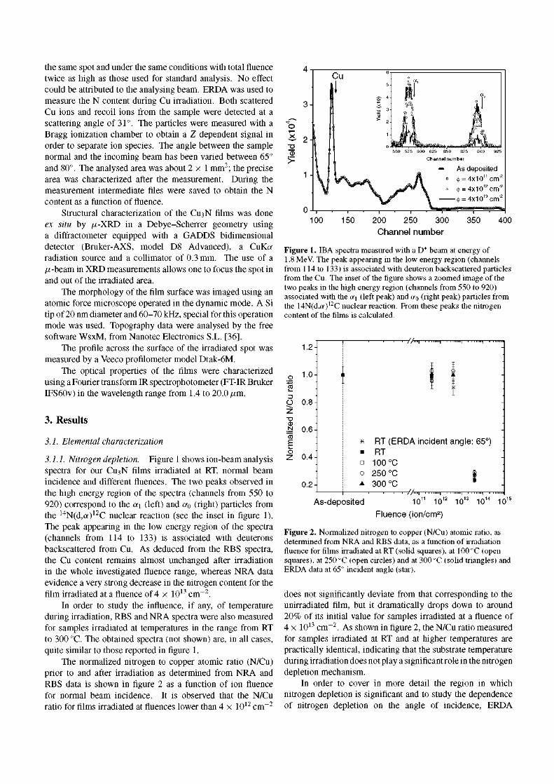
3.1.1. Nitrogen depletion. Figure 1 shows ion-beam analysis spectra for our Cu3N films irradiated at RT, normal beam incidence and different fluences. The two peaks observed in the high energy región of the spectra (channels from 550 to 920) correspond to the a\ (left) and a0 (right) particles from the 14N(d,o012C nuclear reaction (see the inset in figure 1). The peak appearing in the low energy región of the spectra (channels from 114 to 133) is associated with deuterons backscattered from Cu. As deduced from the RBS spectra, the Cu content remains almost unchanged after irradiation in the whole investigated fluence range, whereas NRA data evidence a very strong decrease in the nitrogen content for the film irradiated at a fluence of 4 x 10¹³ cirr2.
In order to study the influence, if any, of temperature during irradiation, RBS and NRA spectra were also measured for samples irradiated at temperatures in the range from RT to 300 °C. The obtained spectra (not shown) are, in all cases, quite similar to those reported in figure 1.
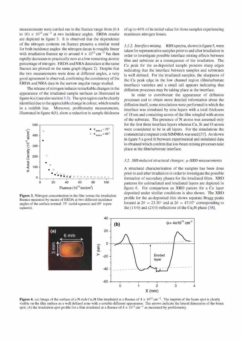
The normalized nitrogen to copper atomic ratio (N/Cu) prior to and after irradiation as determined from NRA and RBS data is shown in figure 2 as a function of ion fluence for normal beam incidence. It is observed that the N/Cu ratio for films irradiated at fluences lower than 4 x 10¹² cirr2
o
>-As deposited
4> = 4x1011cm" i
if = 4x1012 cm''
if = 4x10¹³ c m '
100 150 200 250 300 Channel number
400
Figure 1. IBA spectra measured with a D+ beam at energy of 1.8 MeV. The peak appearing in the low energy región (channels from 114 to 133) is associated with deuteron backscattered particles from the Cu. The inset of the figure shows a zoomed image of the two peaks in the high energy región (channels from 550 to 920) associated with the a1 (left peak) and a0 (right peak) particles from the 14N(d,a)12C nuclear reaction. From these peaks the nitrogen content of the films is calculated.
1.2
13
O
"O
N
1.0
0.8
0.6
0.4
0.2
' I I I / / l i l i 1 1 1
I X
* RT (ERDA incident angle: 65°) • RT • 100°C 0 250°C i A 300°C "
As-deposited 10" 101'
Fluence (¡on/cm2)
101J 101' 101'
Figure 2. Normalized nitrogen to copper (N/Cu) atomic ratio, as determined from NRA and RBS data, as a function of irradiation fluence for films irradiated atRT (solid squares), at 100 °C (open squares), at 250 °C (open circles) and at 300 °C (solid triangles) and ERDA data at 65° incident angle (star).
does not significantly deviate from that corresponding to the unirradiated film, but it dramatically drops down to around 20% of its initial valué for samples irradiated at a fluence of 4 x 10¹³ cirr2. As shown in figure 2, the N/Cu ratio measured for samples irradiated at RT and at higher temperatures are practically identical, indicating that the substrate temperature during irradiation does not play a significant role in the nitrogen depletion mechanism.
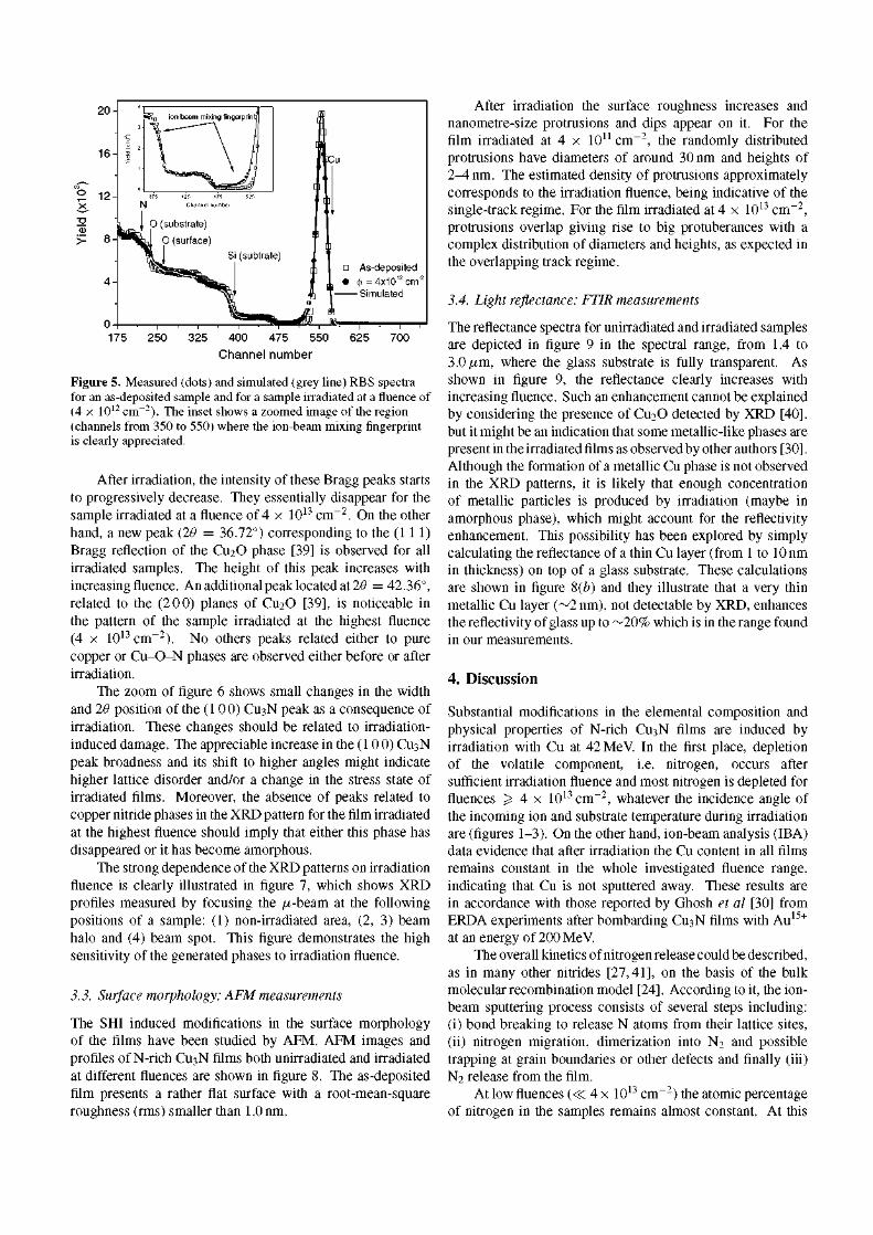
In order to cover in more detail the región in which nitrogen depletion is significant and to study the dependence of nitrogen depletion on the angle of incidence, ERDA
measurements were carried out in the fluence range from (0.4 to 10) x 1013 cirr2 at two incidence angles. ERDA results are depicted in figure 3. It is observed that the dependence of the nitrogen contents on fluence presents a similar trend for both incidence angles: the nitrogen decay is roughly linear with irradiation fluence up to around 4 x 10¹³ cirr2 but then rapidly decreases to practically zero at a low remaining atomic percentage of nitrogen. ERDA and NRA data taken at the same fluence are plotted on the same graph (figure 2). Despite that the two measurements were done at different angles, a very good agreement is observed, confirming the consistency of the ERDA and NRA data in the narrow angular range studied.
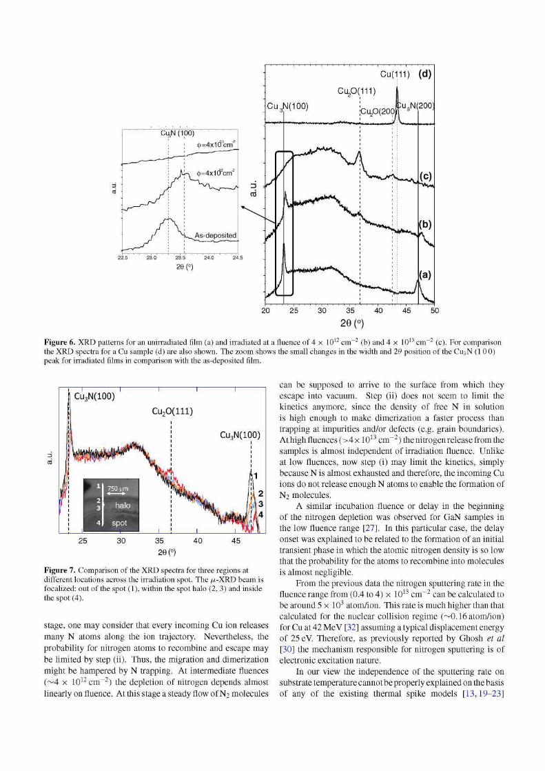
The reléase of nitrogen induces remarkable changes in the appearance of the irradiated sample surfaces as illustrated in figure 4(a) (see also section 3.3). The spot región can be clearly identified due to the appreciable change in colour, which results in a reddish hue. Moreover, profilometry measurements, illustrated in figure 4(b), show a reduction in sample thickness
E o i . to
500
400
r^ 300
O 200
100
• O t f n D D n D D D D D D D
0 20 40 60 80 100
Fluence (1012 ion/cm2)
Figure 3. Nitrogen concentration in the film versus the irradiation fluence measures by means of ERDA at two different incidence angles of the surface normal: 75° (solid squares) and 65° (open squares).
of up to 40% of its initial valué for those samples experiencing máximum nitrogen losses.
3.1.2. Interface mixing. RBS spectra, shown in figure 5, were taken for representative samples prior to and after irradiation in order to investígate possible interface mixing effects between film and substrate as a consequence of the irradiation. The Cu peak for the as-deposited sample presents sharp edges indicating that the interface between samples and substrates is well defined. For the irradiated samples, the sharpness of the Cu peak edge in the low channel región (film/substrate interface) vanishes and a small tail appears indicating that diffusion processes may be taking place at the interface.
In order to corrobórate the appearance of diffusion processes and to obtain more detailed information about the diffusion itself, some simulations were performed in which the interface was simulated by nine layers with a total thickness of 18 nm and containing atoms of the film mingled with atoms of the substrate. The presence of N atoms was assumed only for the first three interface layers whereas Cu, Si and O atoms were considered to be in all layers. For the simulations the commercial computer code SDVINRA was used [37]. As shown in figure 5 a good fit between experimental and simulated data is obtained which confirm that ion-beam mixing processes take place at the film/substrate interface.
3.2. SHI-induced structural changes: /¿-XRD measurements
A structural characterization of the samples has been done prior to and after irradiation in order to investígate the possible formation of secondary phases for the irradiated films. XRD patterns for unirradiated and irradiated layers are depicted in figure 6. For comparison an XRD pattern for a Cu layer deposited under similar conditions is also shown. The XRD profile for the as-deposited film shows sepárate Bragg peaks located at 29 = 23.30° and at 29 = 47.07° corresponding to the (1 0 0) and (2 0 0) reflections of the Cu3N phase [38].
40
>-
20 -
^ 0
-20
-40
-60
(b) ( | )=4x101 3cm"2
X ( m m )
Figure 4. (a) Image of the surface of a N-rich CU3N film irradiated at a fluence of 4 x 10¹³ cirT2. The imprint of the beam spot is clearly visible on the film surface as a well defined zone with a notable different appearance. The arrows indicate the lateral dimensión of the beam spot, (b) the irradiation spot profile for a film irradiated at a fluence of 4 x 10¹³ cirT2 as measured by profilometry.
175 250 325 400 475 550 625 700
Channel number
Figure 5. Measured (dots) and simulated (grey line) RBS spectra for an as-deposited sample and for a sample irradiated at a fluence of (4 x 1012 cm~2). The inset shows a zoomed image of the región (channels from 350 to 550) where the ion-beam mixing fingerprint is clearly appreciated.
After irradiation, the intensity of these Bragg peaks starts to progressively decrease. They essentially disappear for the sample irradiated at a fluence of 4 x 10¹³ cirr2. On the other hand, a new peak (20 = 36.72°) corresponding to the (11 1) Bragg reflection of the Q12O phase [39] is observed for all irradiated samples. The height of this peak increases with increasing fluence. An additional peak located at 20 =42.36°, related to the (2 0 0) planes of Q12O [39], is noticeable in the pattern of the sample irradiated at the highest fluence (4 x 10¹³ cirr2). No others peaks related either to puré copper or Cu-O-N phases are observed either before or after irradiation.
The zoom of figure 6 shows small changes in the width and 20 position of the (100) Q13N peak as a consequence of irradiation. These changes should be related to irradiation-induced damage. The appreciable increase in the (10 0) Q13N peak broadness and its shift to higher angles might indicate higher lattice disorder and/or a change in the stress state of irradiated films. Moreover, the absence of peaks related to copper nitride phases in the XRD pattern for the film irradiated at the highest fluence should imply that either this phase has disappeared or it has become amorphous.
The strong dependence of the XRD patterns on irradiation fluence is clearly illustrated in figure 7, which shows XRD profiles measured by focusing the /x-beam at the following positions of a sample: (1) non-irradiated área, (2, 3) beam halo and (4) beam spot. This figure demonstrates the high sensitivity of the generated phases to irradiation fluence.
3.3. Surface morphology: AFM measurements
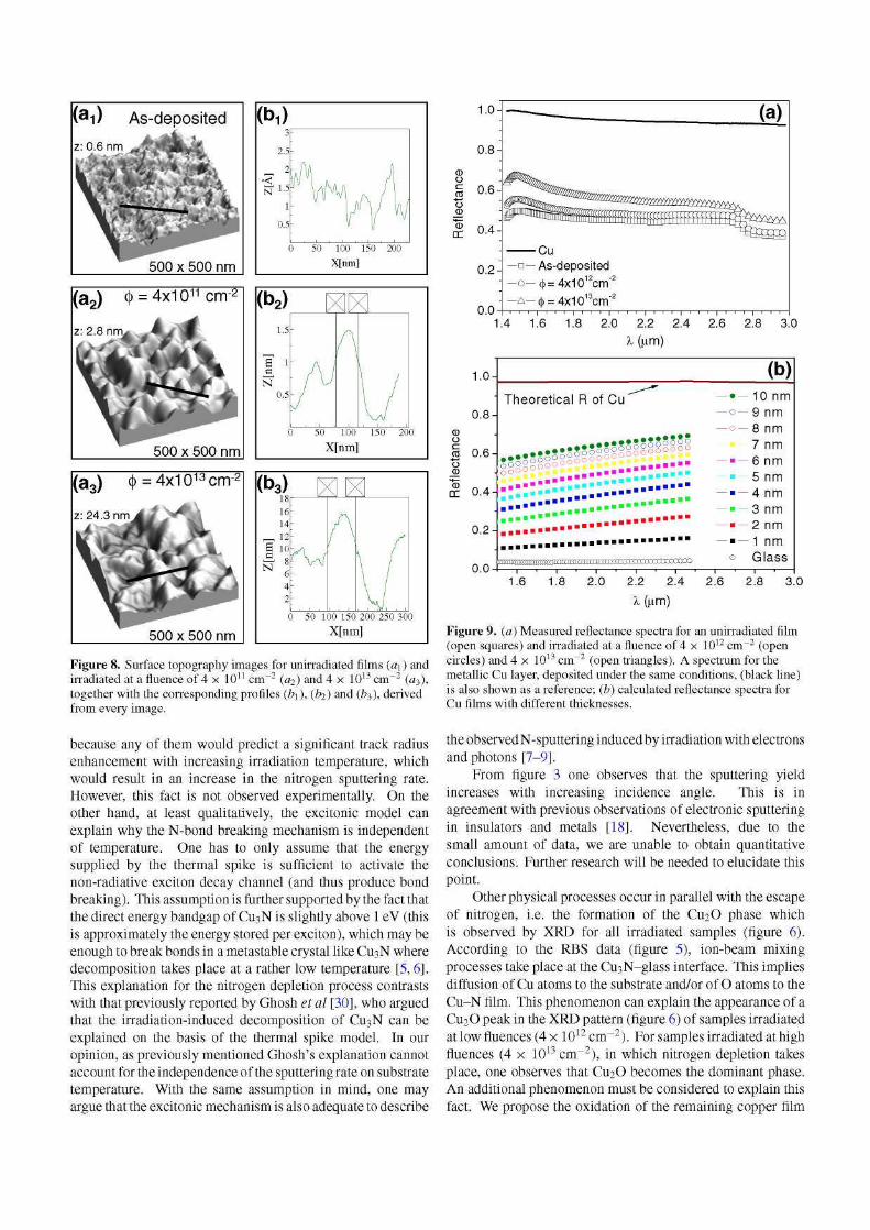
The SHI induced modifications in the surface morphology of the films have been studied by AFM. AFM images and profiles of N-rich Cu3N films both unirradiated and irradiated at different fluences are shown in figure 8. The as-deposited film presents a rather fíat surface with a root-mean-square roughness (rms) smaller than 1.0 nm.
After irradiation the surface roughness increases and nanometre-size protrusions and dips appear on it. For the film irradiated at 4 x 10¹¹ cirr2, the randomly distributed protrusions have diameters of around 30 nm and heights of 2-A nm. The estimated density of protrusions approximately corresponds to the irradiation fluence, being indicative of the single-track regime. For the film irradiated at 4 x 1013 cm~2, protrusions overlap giving rise to big protuberances with a complex distribution of diameters and heights, as expected in the overlapping track regime.
3.4. Light reflectance: FTIR measurements
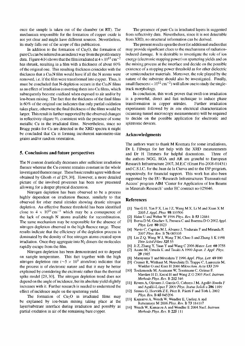
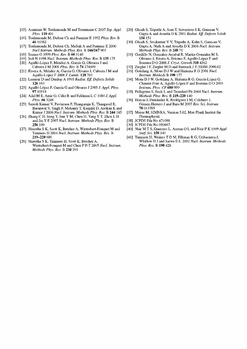
The reflectance spectra for unirradiated and irradiated samples are depicted in figure 9 in the spectral range, from 1.4 to 3.0/xm, where the glass substrate is fully transparent. As shown in figure 9, the reflectance clearly increases with increasing fluence. Such an enhancement cannot be explained by considering the presence of Cu20 detected by XRD [40], but it might be an indication that some metallic-like phases are present in the irradiated films as observed by other authors [30]. Although the formation of a metallic Cu phase is not observed in the XRD patterns, it is likely that enough concentration of metallic particles is produced by irradiation (maybe in amorphous phase), which might account for the reflectivity enhancement. This possibility has been explored by simply calculating the reflectance of a thin Cu layer (from 1 to 10 nm in thickness) on top of a glass substrate. These calculations are shown in figure 8(b) and they illustrate that a very thin metallic Cu layer (~2 nm), not detectable by XRD, enhances the reflectivity of glass up to ~20% which is in the range found in our measurements.
4. Discussion
Substantial modifications in the elemental composition and physical properties of N-rich Q13N films are induced by irradiation with Cu at 42MeV. In the first place, depletion of the volatile component, i.e. nitrogen, occurs after sufficient irradiation fluence and most nitrogen is depleted for fluences ) 4 x 10¹³ cirr2, whatever the incidence angle of the incoming ion and substrate temperature during irradiation are (figures 1-3). On the other hand, ion-beam analysis (IBA) data evidence that after irradiation the Cu content in all films remains constant in the whole investigated fluence range, indicating that Cu is not sputtered away. These results are in accordance with those reported by Ghosh et al [30] from ERDA experiments after bombarding Q13N films with Au15+
at an energy of 200 MeV. The overall kinetics of nitrogen reléase could be described,
as in many other nitrides [27,41], on the basis of the bulk molecular recombination model [24]. According to it, the ion-beam sputtering process consists of several steps including: (i) bond breaking to reléase N atoms from their lattice sites, (ii) nitrogen migration, dimerization into N2 and possible trapping at grain boundaries or other defects and finally (iii) N2 reléase from the film.
At low fluences «C 4 x 10¹³ cirr2) the atomic percentage of nitrogen in the samples remains almost constant. At this
Cu„N(100)
Cu(111) (d)
Cu,0(111)
;Cu,O(200 u3N(200)
Figure 6. XRD patterns for an unirradiated film (a) and irradiated at a fluence of 4 x 10¹² cirT2 (b) and 4 x 10¹³ cirT2 (c). For comparison the XRD spectra for a Cu sample (d) are also shown. The zoom shows the small changes in the width and 26 position of the C113N (1 0 0) peak for irradiated films in comparison with the as-deposited film.
Cu3N(100)
Cu20(lll)
Cu3N(100)
Figure 7. Comparison of the XRD spectra for three regions at different locations across the irradiation spot. The /x-XRD beam is focalized: out of the spot (1), within the spot halo (2, 3) and inside the spot (4).
stage, one may consider that every incoming Cu ion releases many N atoms along the ion trajectory. Nevertheless, the probability for nitrogen atoms to recombine and escape may be limited by step (ii). Thus, the migration and dimerization might be hampered by N trapping. At intermedíate fluences (~4 x 10¹² cirr2) the depletion of nitrogen depends almost linearly on fluence. At this stage a steady flow of N2 molecules
can be supposed to arrive to the surface from which they escape into vacuum. Step (ii) does not seem to limit the kinetics anymore, since the density of free N in solution is high enough to make dimerization a faster process than trapping at impurities and/or defects (e.g. grain boundaries). At high fluences (>4xl0 1 3cm - 2 ) the nitrogen reléase from the samples is almost independent of irradiation fluence. Unlike at low fluences, now step (i) may limit the kinetics, simply because N is almost exhausted and therefore, the incoming Cu ions do not reléase enough N atoms to enable the formation of N2 molecules.
A similar incubation fluence or delay in the beginning of the nitrogen depletion was observed for GaN samples in the low fluence range [27]. In this particular case, the delay onset was explained to be related to the formation of an initial transient phase in which the atomic nitrogen density is so low that the probability for the atoms to recombine into molecules is almost negligible.
From the previous data the nitrogen sputtering rate in the fluence range from (0.4 to 4) x 1013 cm~2 can be calculated to be around 5 x 10³ atom/ion. This rate is much higher than that calculated for the nuclear collision regime (~0.16 atom/ion) for Cu at 42 MeV [32] assuming a typical displacement energy of 25 eV. Therefore, as previously reported by Ghosh et al [30] the mechanism responsible for nitrogen sputtering is of electronic excitation nature.
In our view the independence of the sputtering rate on substrate temperaturecannotbeproperly explained on thebasis of any of the existing thermal spike models [13,19-23]
As-deoosited
500 x 500 nm
(a2) 4) = 4x10¹¹ cnr2
z: 2.8 nm.
500 x 500 nm
(b2)
1.5
'a i N
0.5
(
x A
J ) 50 100 150 20
X[nm] 0
(a3) ^ = 4xl013cm-;
z: 24.3 i
500 x 500 nm 0 50 100 150 200 250 300
X[nm]
Figure 8. Surface topography images for unirradiated films (a\) and irradiated at a fluence of 4 x 10n cirT2 (a2) and 4 x 10¹³ cirT2 (a3), together with the corresponding profiles (b\), (fe) and (¿3), derived from every image.
because any of them would predict a significant track radius enhancement with increasing irradiation temperature, which would result in an increase in the nitrogen sputtering rate. However, this fact is not observed experimentally. On the other hand, at least qualitatively, the excitonic model can explain why the N-bond breaking mechanism is independent of temperature. One has to only assume that the energy supplied by the thermal spike is sufficient to activate the non-radiative exciton decay channel (and thus produce bond breaking). This assumption is further supported by the fact that the direct energy bandgap of Cu3N is slightly above 1 eV (this is approximately the energy stored per exciton), which may be enough to break bonds in a metastable crystal like CU3N where decomposition takes place at a rather low temperature [5,6]. This explanation for the nitrogen depletion process contrasts with that previously reported by Ghosh et al [30], who argued that the irradiation-induced decomposition of Cu3N can be explained on the basis of the thermal spike model. In our opinión, as previously mentioned Ghosh's explanation cannot account for the independence of the sputtering rate on substrate temperature. With the same assumption in mind, one may argüe that the excitonic mechanism is also adequate to describe
o
o
rr
1.0-
0.8-
0.6-
0.4-
0.2-
0.0-
ía)
Cu —•—As-deposited -o-<|)=4x1012cm"2
-A - ( | ) = 4xio13cm"2
1.4 1.6 1.8 2.0 2.2 2.4 2.6 2.8 X (Lim)
3.0
1.0
0.8-
O
Jj 0.6-o
_<t>
I 0.4
0.2
0.0
(b)
Theoretical R of Cu'
0 0 0 2 2 A 5 6 0 0 - -3 0 0 0 0 0 c
•SSS'ooooOO _„ooc
— • — — 0 —
— 0 —
— • -
— • -
— • -
— • -
— • -
— • -
0
10 nm 9 8 7 6 5 4 3 2 1
nm nm nm nm nm nm nm nm nm
Glass
1.6 1.8 2.0 — i — 2.2 2.4 2.6 2.8 3.0
X (nm)
Figure 9. (a) Measured reflectance spectra for an unirradiated film (open squares) and irradiated at a fluence of 4 x 1012 cm~2 (open circles) and 4 x 10¹³ cirT2 (open triangles). A spectrum for the metallic Cu layer, deposited under the same conditions, (black line) is also shown as a reference; (b) calculated reflectance spectra for Cu films with different thicknesses.
the observed N-sputtering inducedby irradiation with electrons andphotons [7-9].
From figure 3 one observes that the sputtering yield increases with increasing incidence angle. This is in agreement with previous observations of electronic sputtering in insulators and metáis [18]. Nevertheless, due to the small amount of data, we are unable to obtain quantitative conclusions. Further research will be needed to elucidate this point.
Other physical processes occur in parallel with the escape of nitrogen, i.e. the formation of the Q12O phase which is observed by XRD for all irradiated samples (figure 6). According to the RBS data (figure 5), ion-beam mixing processes take place at the Qi3N-glass interface. This implies diffusion of Cu atoms to the substrate and/or of O atoms to the Cu-N film. This phenomenon can explain the appearance of a Cu20 peak in the XRD pattern (figure 6) of samples irradiated at low fiuences (4 x 10¹² cirr2). For samples irradiated at high fiuences (4 x 10¹³ cirr2), in which nitrogen depletion takes place, one observes that CU2O becomes the dominant phase. An additional phenomenon must be considered to explain this fact. We propose the oxidation of the remaining copper film
once the sample is taken out of the chamber (at RT). The mechanism responsible for the formation of copper oxide is not yet clear and might have different sources. Nevertheless, its study falls out of the scope of this publication.
In addition to the formation of C112O, the formation of puré Cu can be inferred in an indirect way from the profilometry data. Figure4(fc)showsthatthefilmirradiatedat4x 1013cirr2
has shrunk, resulting in a film with a thickness of about 60% of the original one. This resulting thickness coincides with the thickness that a Q13N film would have if all the N atoms were removed, i.e. if the film were transformed into copper. Thus, it must be concluded that N-depletion occurs in the CU3N films as an effect of irradiation converting them into Cu films, which subsequently become oxidized when exposed to air and/or by ion-beam mixing. The fact that the thickness of the final films is 60% of the original one indicates that only partial oxidation takes place, otherwise the final thickness of the films would be larger. This result is further supported by the observed changes in refiectivity (figure 9), consistent with the presence of some metallic Cu in the irradiated films. Nevertheless, since no Bragg peaks for Cu are detected in the XRD spectra it might be concluded that Cu is forming incoherent nanometre-size grains and/or random orientation.
5. Conclusions and future perspectives
The N content drastically decreases after sufficient irradiation fiuence whereas the Cu content remains constant in the whole investigated fiuence range. These basic results agree with those obtained by Ghosh et al [29,30]. However, a more detailed picture of the involved processes has been now presented allowing for a deeper physical discussion.
Nitrogen depletion has been observed to be a process highly dependent on irradiation fiuence, similarly to that observed for other metal nitrides showing drastic nitrogen depletion. An effective fiuence threshold has been identified cióse to 4 x 10¹² cirr2 which may be a consequence of the lack of enough N atoms available for recombination. The same mechanism may be responsible for the absence of nitrogen depletion observed in the high fiuence range. These results indicate that the efficiency of the depletion process is dominated by the density of free nitrogen atoms created upon irradiation. Once they aggregate into N2 dimers the molecules rapidly escape from the film.
Nitrogen depletion has been demonstrated not to depend on sample temperature. This fact together with the high nitrogen depletion rate (~5 x 10³ atom/ion) indicates that the process is of electronic nature and that it may be better explained by considering the excitonic rather than the thermal spike model [29,30]. The nitrogen depletion trend does not depend on the angle of incidence, but its absolute yield slightly increases with it. Further research is needed to understand the effect of incidence angle on the sputtering yield.
The formation of CU2O in irradiated films may be explained by ion-beam mixing taking place at the layer/substrate interface during irradiation and possibly as partial oxidation in air of the remaining bare copper.
The presence of puré Cu in irradiated layers is suggested from refiectivity data. Nevertheless, since it is not detectable from XRD, no structural information can be derived.
The present results open the door for additional studies that may provide significant clues to the mechanisms of radiation-induced damage. It is desirable to investígate the role of ion energy (electronic stopping power) on sputtering yields and on the mixing process at the interface and decide on the possible existence of a stopping power threshold as for other dielectric or semiconductor materials. Moreover, the role played by the nature of the substrate should also be investigated. Finally, small fiuences (< 1012 cirr2) will allow one to study the single-track morphology.
In conclusión, this work proves that swift-ion irradiation is a powerful, direct and fast technique to induce phase transformation in copper nitrides. Further irradiation experiments followed by in situ electrical characterization (scanning tunnel microscopy measurements) will be required to decide on the possible application for electronic and spintronic devices.
Acknowledgments
The authors want to thank M Kosmata for some irradiations, Dr L Fábrega for her help with the XRD measurements and Dr H Timmers for help ful discussions. Three of the authors NGG, RGA and AR are grateful to European Research Infrastructure 2007, M.E.C (GrantFis-2008-01431) and C.S.I.C. for the Juan de la Cierva and to the I3P program, respectively, for financial support. This work has also been supported by the EU- 'Research Infrastructures Transnational Access' program ADVI 'Center for Application of Ion Beams in Materials Research' under EC contract no 025646.
References
[i]
[2;
[3
[4;
[5 [6; [7
[»; [9;
[10;
[ii
[12;
[13
[14
Yue G H, Yan P X, Liu J Z, Wang M X, Li M and Xuan X M 2005 /. Appl. Phys. 98 103506
Hahn U and Weber W 1996 Phys. Rev. B 53 12684 Borsa D M, Grachev S, Presura C and Boerma D O 2002 Appl.
Phys. Lett. 80 1823 Navio C, Capitán M J, Álvarez J, Yndurain F and Miranda R
2007 Phys. Rev. B 76 085105 Liu Z Q, Wang W J, Wang T M, Chao S and Zheng S K 1998
Thin Solid Films 325 55 Ji Z, Zhang Y Yuan Y and Wang C 2006 Maten Lett. 60 3758 Asano M, Umeda K and Tasaki A 1990 Japan. J. Appl. Phys.
29 1985 Maruyama T and Morishita T 1996 Appl. Phys. Lett. 69 890 Cremer R, Witthaut M, Neuschütz D, Trappe C, Laurenzis M,
Winkler O and Kurz H 2000 Mikrochim. Acta 133 299 Toulemonde M, Assmann W, Trautmann C, Grüner F,
Mieskes H D, Kucal H and Wang Z G 2003 Nucí. Instrum. Methods Phys. Res. B 212 346
Rivera A, Olivares J, García G, Cabrera J M, Agulló-Rueda F and Agulló-López F 2009 Phys. Status Solidi a 206 1109
Szenes G, Horváth Z E, Pécz B, Pászti F and Tóth L 2002 Phys. Rev. B 65 045206
Kamarou A, Wesch W, Wendler E, Undisz A and Rettenmayr M 2006 Phys. Rev. B 73 184107
Wesch W, Kamarou A and Wendler E 2004 Nucí. Instrum. Methods Phys. Res. B 225 111
[15] Assmann W, Toulemonde M and Trautmann C 2007 Top. Appl. Phys. 110 401
[16] Toulemonde M, Dufour Ch and Paumier E 1992 Phys. Rev. B 46 14362
[17] Toulemonde M, Dufour Ch, Meftah A and Paumier E 2000 Nucí Instrum. Methods Phys. Res. B 166/167 903
[18] Szenes G 1999 Phys. Rev. B 60 3140 [19] Itoh N 1998 Nucí. Instrum. Methods Phys. Res. B 135 175 [20] Agulló-López F, Méndez A, García G, Olivares J and
Cabrera J M 2006 Phys. Rev. B 74 174109 [21] Rivera A, Méndez A, García G, Olivares J, Cabrera J M and
Agulló-López F 2008 /. Lumin. 128 703 [22] Lesueur D and Dunlop A 1993 Radiat. Eff. Defects Solids
126 163 [23] Agulló-López F, García G and Olivares J 2005 /. Appl. Phys.
97 93514 [24] Adel M E, Amir O, Cáliz R and Feldman L C 1989 /. Appl.
Phys. 66 3248 [25] Suresh Kumar V, Puviarasu P, Thangaraju K, Thangavel R,
Baranwal V, Singh F, Mohánty T, Kanjilal D, Asokan K and Kumar J 2006 Nucí. Instrum. Methods Phys. Res. B 244 145
[26] Zhang C H, Song Y, Sun Y M, Chen H, Yang Y T, Zhou L H and Jin Y F 2007 Nucí. Instrum. Methods Phys. Res. B 256 199
[27] Shrestha S K, Scott K, Butcher A, Wintrebert-Fouquet M and Timmers H 2004 Nucí. Instrum. Methods Phys. Res. B 219-220 686
[28] Shrestha S K, Timmers H, Scott K, Butcher A, Wintrebert-Fouquet M and Chen P P-T 2005 Nucí. Instrum. Methods Phys. Res. B 234 291
[29] Ghosh S, Tripathi A, Som T, Srivastava S K, Ganesan V, Gupta A and Avasthi D K 2001 Radiat. Eff. Defects Solids 154 151
[30] Ghosh S, Sivakumar V V, Tripathi A, Kahn S, Ganesan V, Gupta A, Nath A and Avasthi D K 2006 Nucí. Instrum. Methods Phys. Res. B 248 71
[31] Gordillo N, González-Arrabal R, Martin-Gonzalez M S, Olivares J, Rivera A, Briones F, Agulló-López F and Boerma D O 2008 /. Cryst. Growth 310 4362
[32] Ziegler J F, Ziegler M D and Biersack J P, SRIM-2006.02 [33] Gottdang A, Mous D J W and Haitsma R G 2001 Nucí.
Instrum. Methods B 190 177 [34] Mous D J W, Gottdang A, Haitsma R G, García-López G,
Climent-Font A, Agulló-López F and Boerma D O 2003 Instrum. Phys. CP 680 999
[35] Pellegrino S, Beck L and Trouslard Ph 2004 Nucí. Instrum. Methods Phys. Res. B 219-220 140
[36] Horcas I, Fernández R, Rodríguez J M, Colchero J, Gómez-Herrero J and Baro M 2007 Rev. Sci. Instrum. 78 013705
[37] Mayer M, SIMNRA, Versión 5.02, Max Plank Institut für Plasmaphysik
[38] JCPDS File No 471088 [39] JCPDS File No 050667 [40] Nair M T S, Guerrero L, Arenas O L and Nair P K 1999 Appl.
Surf. Sci. 150 143 [41] Timmers H, Weijers T D M, Elliman R G, Uribasterra J,
Whitlow H J and Sarwe E-L 2002 Nucí. Instrum. Methods Phys. Res. B 190 428