Embed Size (px)
Citation preview
International Journal of Research Studies in Electrical and Electronics Engineering (IJRSEEE)
Volume 1, Issue 2, July - September 2015, PP 1-17
www.arcjournals.org
©ARC Page | 1
Comprehensive Analysis of Discontinuous Space Vector PWM
Techniques for a Five-Phase Voltage Source Inverter
Mohd. Arif Khan
School of Electrical & Electronics Engineering
College of Engineering, Science &Technology Fiji National University, FIJI
Abstract: This paper develops discontinuous space vector PWM (DPWM) technique for a five-phase voltage
source inverter (VSI). Space vector model of a five-phase VSI shows that there exist 32 space vectors with three
different lengths forming three concentric decagons. Application of outer most and middle set of space vectors
to implement Space vector PWM yield nearly sinusoidal output. Thus the proposed DPWM utilises the same set
of space vectors to implement the modulation techniques. Performance is evaluated in terms of total harmonic
distortion and weighted total harmonic distortion in output phase voltages. A significant reduction in switching
losses is observed. The simulation results are provided to validate the concept.
1. INTRODUCTION
Multi-phase motor drives have gained much popularity in recent years and a number of research papers have been published. The main reason is the inherent advantages offered by multi-phase
motors such as reduction in the amplitude and increase in the frequency of torque pulsation, reduction
in the rotor current harmonics, reduction in the dc link current harmonics, reduction in the current per phase without increasing the voltage per phase leading and increasing the torque per ampere for the
same volume machine. Keeping in view these advantages the application of multi-phase motors are
coming up mainly in high power ranges such as ship propulsion, electric and hybrid vehicles, aircraft fuel pump applications etc. A review on multi-phase motor drives is available in [1,2]. Multi-phase
motors need invariably some sort of power electronic converter for their supply as phases more than
three is not readily available from the grid. The most common choice is a multi-phase voltage source inverter. There are mainly two methods of controlling the output voltage and frequency of inverters
namely; square wave mode and pulse width modulation mode. A number of PWM techniques are
available to control a three-phase VSI [3, 4]. However, Space Vector Pulse Width Modulation
(SVPWM) has become the most popular method because of the easiness of digital implementation and better DC bus utilisation, when compared to the ramp-comparison sinusoidal PWM method.
Another PWM method known as Discontinuous PWM is widely used because it offers reduced
number of switching and consequently reduced switching losses. This aspect becomes extremely important when dealing with high power drive system, as even a small saving in switching losses
means a large amount of overall power saving and thus enhanced energy efficiency of motors.
In principle, there is a lot of flexibility available in choosing the proper space vector combination for implementing space vector PWM for a multi-phase VSI. Space vector PWM technique for a five-
phase VSI is illustrated in [5-10], where continuous mode is considered. This paper takes up issue of
space vector PWM for a five-phase VSI in discontinuous mode. It is shown that the number of
switching and consequently the switching losses can be greatly reduced by tiding one or more inverter legs to either positive or negative DC bus. This is termed as discontinuous space vector PWM which
is developed for a five-phase VSI in this paper. Discontinuous space vector PWM is also available for
a five-phase VSI in [11] where natural extension of three-phase discontinuous PWM was done and only large length vectors were used. Although the maximum possible fundamental output is high
equal to 0.6115 p.u. but the output contain low-order harmonics. The switching is reduced by 40%
compared to the continuous SVPWM. This paper utilises large and medium length space vectors to
implement discontinuous SVPWM, providing sinusoidal output phase voltages. Similar discontinuous space vector PWM techniques are available in [12]. However, paper does not provide detail of the
common mode voltage and other aspect of the PWM. In contrast this paper illustrates leg voltages,
common mode voltages and the amount of reduction in switching due to each scheme. Moreover, two
Mohd. Arif Khan
International Journal of Research Studies in Electrical and Electronics Engineering (IJRSEEE) Page | 2
novel methods are proposed in this paper, which yield better results compared to the existing schemes. The simulation results are provided to support the findings.
2. MODELING OF A FIVE-PHASE VSI
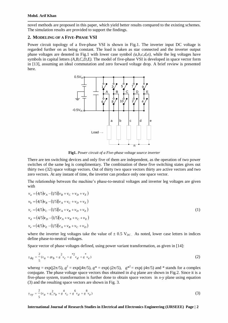
Power circuit topology of a five-phase VSI is shown in Fig.1. The inverter input DC voltage is regarded further on as being constant. The load is taken as star connected and the inverter output
phase voltages are denoted in Fig.1 with lower case symbol (a,b,c,d,e), while the leg voltages have
symbols in capital letters (A,B,C,D,E). The model of five-phase VSI is developed in space vector form in [13], assuming an ideal commutation and zero forward voltage drop. A brief review is presented
here.
0.5Vdc
1 3 5 7 9
6 8 10 4
A B C D E
a b c d e
n
Load
2
-0.5Vdc
Fig1. Power circuit of a Five-phase voltage source inverter
There are ten switching devices and only five of them are independent, as the operation of two power switches of the same leg is complimentary. The combination of these five switching states gives out
thirty two (32) space voltage vectors. Out of thirty two space vectors thirty are active vectors and two
zero vectors. At any instant of time, the inverter can produce only one space vector.
The relationship between the machine’s phase-to-neutral voltages and inverter leg voltages are given with
EDCBAa vvvvvv 5154
EDCABb vvvvvv 5154
EDBACc vvvvvv 5154 (1)
ECBADd vvvvvv 5154
DCBAEe vvvvvv 5154
where the inverter leg voltages take the value of ± 0.5 VDC . As noted, lower case letters in indices define phase-to-neutral voltages.
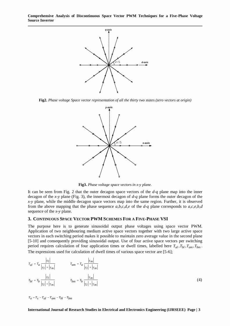
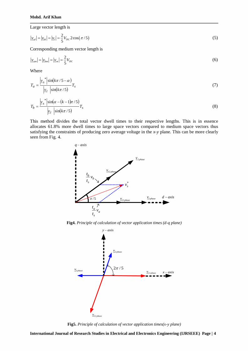
Space vector of phase voltages defined, using power variant transformation, as given in [14]:
)*2*2
(
5
2
evadvacvabvaavdqv (2)
wherea = exp(j2/5), a2 = exp(j4/5), a* = exp(-j2/5), a*
2 = exp(-j4/5) and * stands for a complex
conjugate. The phase voltage space vectors thus obtained in d-q plane are shown in Fig.2. Since it is a
five-phase system, transformation is further done to obtain space vectors in x-y plane using equation
(3) and the resulting space vectors are shown in Fig. 3.
)8642
(
5
2
evadvacvabvaavxyv (3)
Comprehensive Analysis of Discontinuous Space Vector PWM Techniques for a Five-Phase Voltage
Source Inverter
International Journal of Research Studies in Electrical and Electronics Engineering (IJRSEEE) Page | 3
/ 5
q-axis
d-axis
Fig2. Phase voltage Space vector representation of all the thirty two states (zero vectors at origin)
/ 5
y-axis
x-axis
Fig3. Phase voltage space vectors in x-y plane.
It can be seen from Fig. 2 that the outer decagon space vectors of the d-q plane map into the inner decagon of the x-y plane (Fig. 3), the innermost decagon of d-q plane forms the outer decagon of the
x-y plane, while the middle decagon space vectors map into the same region. Further, it is observed
from the above mapping that the phase sequence a,b,c,d,e of the d-q plane corresponds to a,c,e,b,d sequence of the x-y plane.
3. CONTINUOUS SPACE VECTOR PWM SCHEMES FOR A FIVE-PHASE VSI
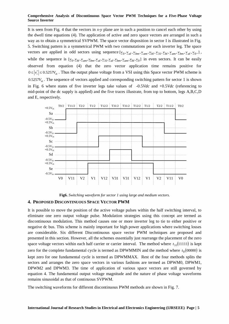
The purpose here is to generate sinusoidal output phase voltages using space vector PWM. Application of two neighbouring medium active space vectors together with two large active space
vectors in each switching period makes it possible to maintain zero average value in the second plane
[5-10] and consequently providing sinusoidal output. Use of four active space vectors per switching
period requires calculation of four application times or dwell times, labelled here bmamblal TTTT ,,, .
The expressions used for calculation of dwell times of various space vector are [5-6];
mvlv
lv
aTalT
mvlv
mv
aTamT
mvlv
lv
bTblT
mvlv
mv
bTbmT
(4)
bmTblTamTalTsToT
Mohd. Arif Khan
International Journal of Research Studies in Electrical and Electronics Engineering (IJRSEEE) Page | 4
Large vector length is
2
2cos / 55
DCal bl lv v v V (5)
Corresponding medium vector length is
2
5DCam bm mv v v V (6)
Where
s
l
s
a Tkv
kvT
5/sin
5/sin*
(7)
s
l
s
b Tkv
kvT
5/sin
5/1sin*
(8)
This method divides the total vector dwell times to their respective lengths. This is in essence
allocates 61.8% more dwell times to large space vectors compared to medium space vectors thus
satisfying the constraints of producing zero average voltage in the x-y plane. This can be more clearly seen from Fig. 4.
1phasev
2 phasev
11phasev
12 phasev
q axis
d axis/ 5
*sv
aa
s
tv
t
bb
s
tv
t
Fig4. Principle of calculation of vector application times (d-q plane)
11phasev
2 phasev
1phasev
y axis
x axis
12 phasev
2 / 5
Fig5. Principle of calculation of vector application times(x-y plane)
Comprehensive Analysis of Discontinuous Space Vector PWM Techniques for a Five-Phase Voltage
Source Inverter
International Journal of Research Studies in Electrical and Electronics Engineering (IJRSEEE) Page | 5
It is seen from Fig. 4 that the vectors in x-y plane are in such a position to cancel each other by using
the dwell time equations (4). The application of active and zero space vectors are arranged in such a
way as to obtain a symmetrical SVPWM. The space vector disposition in sector I is illustrated in Fig.
5. Switching pattern is a symmetrical PWM with two commutations per each inverter leg. The space
vectors are applied in odd sectors using sequence ],,,,,,,,,,,[ 0310 vvvvvvvvvvv albmamblblambmal ,
while the sequence is ],,,,,,,,,,[ 0310 vvvvvvvvvvv blambmalalbmambl in even sectors. It can be easily
observed from equation (4) that the zero vector application time remains positive for*0 0.5257s dcv V . Thus the output phase voltage from a VSI using this Space vector PWM scheme is
0.5257 dcV . The sequence of vectors applied and corresponding switching pattern for sector 1 is shown
in Fig. 6 where states of five inverter legs take values of -0.5Vdc and +0.5Vdc (referencing to
mid-point of the dc supply is applied) and the five traces illustrate, from top to bottom, legs A,B,C,D
and E, respectively.
Fig6. Switching waveform for sector 1 using large and medium vectors.
4. PROPOSED DISCONTINUOUS SPACE VECTOR PWM
It is possible to move the position of the active voltage pulses within the half switching interval, to
eliminate one zero output voltage pulse. Modulation strategies using this concept are termed as
discontinuous modulation. This method causes one or more inverter leg to tie to either positive or
negative dc bus. This scheme is mainly important for high power applications where switching losses
are considerable. Six different Discontinuous space vector PWM techniques are proposed and
presented in this section. However, all the schemes essentially just rearrange the placement of the zero
space voltage vectors within each half carrier or carrier interval. The method where 1111131t is kept
zero for the complete fundamental cycle is termed as DPWMMIN and the method where 000000t is
kept zero for one fundamental cycle is termed as DPWMMAX. Rest of the four methods splits the
sectors and arranges the zero space vectors in various fashions are termed as DPWM0, DPWM1,
DPWM2 and DPWM3. The time of application of various space vectors are still governed by
equation 4. The fundamental output voltage magnitude and the nature of phase voltage waveforms
remains sinusoidal as that of continuous SVPWM.
The switching waveforms for different discontinuous PWM methods are shown in Fig. 7.
+0.5Vdc
-0.5Vdc
+0.5Vdc
-0.5Vdc
+0.5Vdc
-0.5Vdc
+0.5Vdc
-0.5Vdc
+0.5Vdc
-0.5Vdc
Sa
Sb
Sc
Sd
Se
V0 V2V1V12V31V31V12V1V2V11 V11 V0
T0/2 T11/2 T31/2 T31/2T2/2 T1/2 T12/2 T1/2 T2/2 T11/2 T0/2T12/2
Mohd. Arif Khan
International Journal of Research Studies in Electrical and Electronics Engineering (IJRSEEE) Page | 6
+0.5Vdc
-0.5Vdc
+0.5Vdc
-0.5Vdc
+0.5Vdc
-0.5Vdc
+0.5Vdc
-0.5Vdc
+0.5Vdc
-0.5Vdc
Sa
Sb
Sc
Sd
Se
V0 V2V1V12V12V1V2V11 V11 V0
T0/2 T11/2 T2/2 T1/2 T12/2 T1/2 T2/2 T0/2T12/2 T11/2
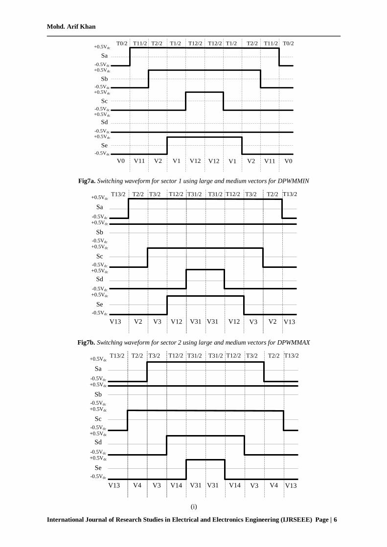
Fig7a. Switching waveform for sector 1 using large and medium vectors for DPWMMIN
+0.5Vdc
-0.5Vdc
+0.5Vdc
-0.5Vdc
+0.5Vdc
-0.5Vdc
+0.5Vdc
-0.5Vdc
+0.5Vdc
-0.5Vdc
V13 V3 V2V12V12V3V2 V31 V13
T13/2 T12/2T2/2 T3/2 T31/2 T3/2 T2/2T31/2 T12/2
V31
Sa
Sb
Sc
Sd
Se
T13/2
Fig7b. Switching waveform for sector 2 using large and medium vectors for DPWMMAX
+0.5Vdc
-0.5Vdc
+0.5Vdc
-0.5Vdc
+0.5Vdc
-0.5Vdc
+0.5Vdc
-0.5Vdc
+0.5Vdc
-0.5Vdc
V13 V3 V4V14V14V3V4 V31 V13
T13/2 T12/2T2/2 T3/2 T31/2 T3/2 T2/2T31/2 T12/2
V31
Sa
Sb
Sc
Sd
Se
T13/2
(i)
Comprehensive Analysis of Discontinuous Space Vector PWM Techniques for a Five-Phase Voltage
Source Inverter
International Journal of Research Studies in Electrical and Electronics Engineering (IJRSEEE) Page | 7
+0.5Vdc
-0.5Vdc
+0.5Vdc
-0.5Vdc
+0.5Vdc
-0.5Vdc
+0.5Vdc
-0.5Vdc
+0.5Vdc
-0.5Vdc
Sa
Sb
Sc
Sd
Se
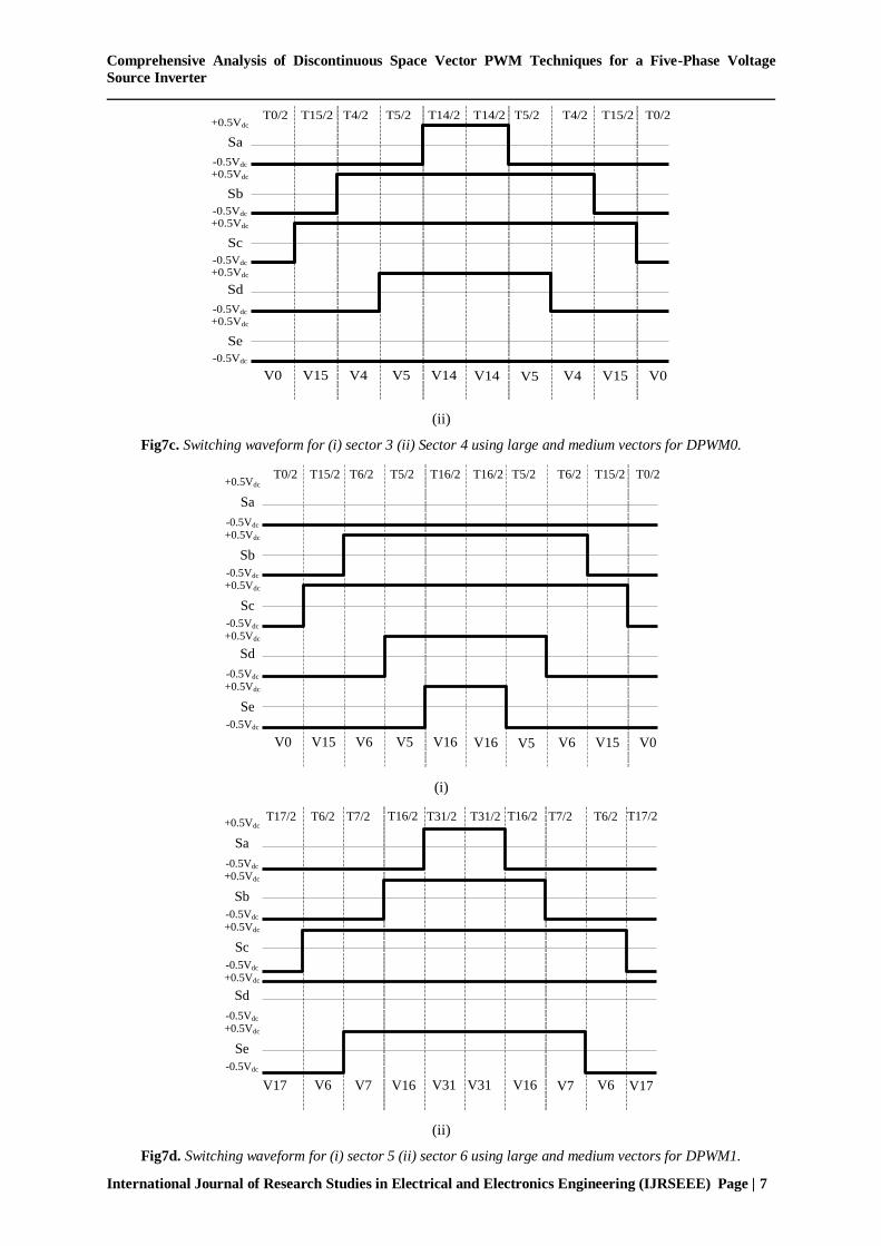
V0 V4V5V14V14V5V4V15 V15 V0
T0/2 T15/2 T4/2 T5/2 T14/2 T5/2 T4/2 T0/2T14/2 T15/2
(ii)
Fig7c. Switching waveform for (i) sector 3 (ii) Sector 4 using large and medium vectors for DPWM0.
+0.5Vdc
-0.5Vdc
+0.5Vdc
-0.5Vdc
+0.5Vdc
-0.5Vdc
+0.5Vdc
-0.5Vdc
+0.5Vdc
-0.5Vdc
Sa
Sb
Sc
Sd
Se
V0 V6V5V16V16V5V6V15 V15 V0
T0/2 T15/2 T6/2 T5/2 T16/2 T5/2 T6/2 T0/2T16/2 T15/2
(i)
+0.5Vdc
-0.5Vdc
+0.5Vdc
-0.5Vdc
+0.5Vdc
-0.5Vdc
+0.5Vdc
-0.5Vdc
+0.5Vdc
-0.5Vdc
V17 V7 V6V16V16V7V6 V31 V17
T17/2 T16/2T6/2 T7/2 T31/2 T7/2 T6/2T31/2 T16/2
V31
Sa
Sb
Sc
Sd
Se
T17/2
(ii)
Fig7d. Switching waveform for (i) sector 5 (ii) sector 6 using large and medium vectors for DPWM1.
Mohd. Arif Khan
International Journal of Research Studies in Electrical and Electronics Engineering (IJRSEEE) Page | 8
+0.5Vdc
-0.5Vdc
+0.5Vdc
-0.5Vdc
+0.5Vdc
-0.5Vdc
+0.5Vdc
-0.5Vdc
+0.5Vdc
-0.5Vdc
V17 V7 V6V16V16V7V6 V31 V17
T17/2 T16/2T6/2 T7/2 T7/2 T6/2T31/2 T16/2
Sa
Sb
Sc
Sd
Se
T17/2
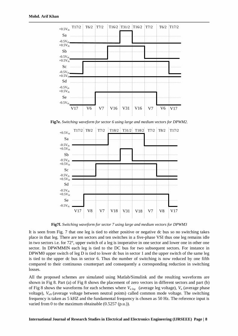
Fig7e. Switching waveform for sector 6 using large and medium vectors for DPWM2.
+0.5Vdc
-0.5Vdc
+0.5Vdc
-0.5Vdc
+0.5Vdc
-0.5Vdc
+0.5Vdc
-0.5Vdc
+0.5Vdc
-0.5Vdc
Sa
Sb
Sc
Sd
Se
V7V18V31V18V7V8V17 V17V8
T17/2 T8/2 T7/2 T31/2 T18/2 T7/2 T8/2T18/2 T17/2
Fig7f. Switching waveform for sector 7 using large and medium vectors for DPWM3
It is seen from Fig. 7 that one leg is tied to either positive or negative dc bus so no switching takes
place in that leg. There are ten sectors and ten switches in a five-phase VSI thus one leg remains idle
in two sectors i.e. for 72°, upper switch of a leg is inoperative in one sector and lower one in other one
sector. In DPWMMIN each leg is tied to the DC bus for two subsequent sectors. For instance in
DPWM0 upper switch of leg D is tied to lower dc bus in sector 1 and the upper switch of the same leg
is tied to the upper dc bus in sector 6. Thus the number of switching is now reduced by one fifth
compared to their continuous counterpart and consequently a corresponding reduction in switching
losses.
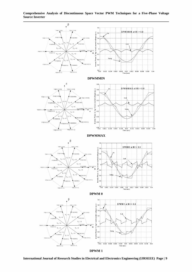
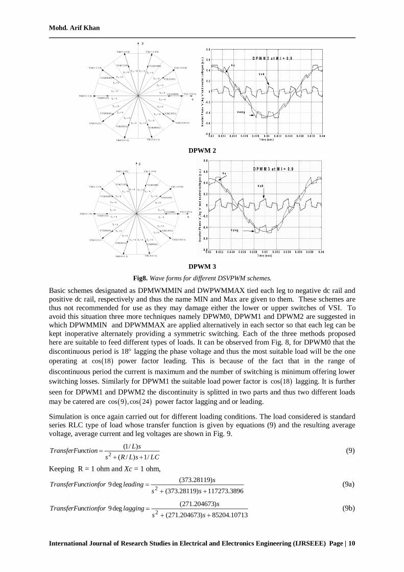
All the proposed schemes are simulated using Matlab/Simulink and the resulting waveforms are
shown in Fig 8. Part (a) of Fig 8 shows the placement of zero vectors in different sectors and part (b)
of Fig 8 shows the waveforms for each schemes where Va leg (average leg voltage), Va (average phase
voltage), VnN (average voltage between neutral points) called common mode voltage. The switching
frequency is taken as 5 kHZ and the fundamental frequency is chosen as 50 Hz. The reference input is
varied from 0 to the maximum obtainable (0.5257 (p.u.)).
Comprehensive Analysis of Discontinuous Space Vector PWM Techniques for a Five-Phase Voltage
Source Inverter
International Journal of Research Studies in Electrical and Electronics Engineering (IJRSEEE) Page | 9
DPWMMIN
DPWMMAX
DPWM 0
DPWM 1
V1(1 1 0 0 1)
V7(0 0 111 )
V8(0 0 0 1 1) V9(1 0 0 1 1)
V10(1 0 0 0 1)
V6(0 0 1 1 0)
V5(0 1 1 1 0)
V4(0 1 1 0 0) V3(1 1 1 0 0)
V2(1 1 0 0 0)
α
β
V11(10000)
V17(00010)
V18(10111) V19(00001)
V20(11011)
V16(01111)
V15(00100)
V14(11110) V13(01000)
V12(11101)
T31 = 0
T31 = 0
T31 = 0
T31 = 0
T31 = 0
T31 = 0T31 = 0
T31 = 0
T31 = 0
T31 = 0
V1(1 1 0 0 1)
V7(0 0 111 )
V8(0 0 0 1 1) V9(1 0 0 1 1)
V10(1 0 0 0 1)
V6(0 0 1 1 0)
V5(0 1 1 1 0)
V4(0 1 1 0 0) V3(1 1 1 0 0)
V2(1 1 0 0 0)
α
β
V11(10000)
V17(00010)
V18(10111) V19(00001)
V20(11011)
V16(01111)
V15(00100)
V14(11110) V13(01000)
V12(11101)
T0 = 0
T0 = 0
T0 = 0
T0 = 0
T0 = 0T0 = 0 T0 = 0
T0 = 0
T0 = 0 T0 = 0
V1(1 1 0 0 1)
V7(0 0 111 )
V8(0 0 0 1 1) V9(1 0 0 1 1)
V10(1 0 0 0 1)
V6(0 0 1 1 0)
V5(0 1 1 1 0)
V4(0 1 1 0 0) V3(1 1 1 0 0)
V2(1 1 0 0 0)
α
β
V11(10000)
V17(00010)
V18(10111) V19(00001)
V20(11011)
V16(01111)
V15(00100)
V14(11110) V13(01000)
V12(11101)T31 = 0
T0 = 0
T31 = 0
T31 = 0
T31 = 0
T0 = 0T0 = 0
T0 = 0
T0 = 0
T31 = 0
V1(1 1 0 0 1)
V7(0 0 111 )
V8(0 0 0 1 1) V9(1 0 0 1 1)
V10(1 0 0 0 1)
V6(0 0 1 1 0)
V5(0 1 1 1 0)
V4(0 1 1 0 0) V3(1 1 1 0 0)
V2(1 1 0 0 0)
α
β
V11(10000)
V17(00010)
V18(10111) V19(00001)
V20(11011)
V16(01111)
V15(00100)
V14(11110) V13(01000)
V12(11101)T0 = 0
T31 = 0
T0 = 0
T31 = 0
T0 = 0
T31 = 0
T0 = 0
T31 = 0
T0 = 0
T31 = 0
Mohd. Arif Khan
International Journal of Research Studies in Electrical and Electronics Engineering (IJRSEEE) Page | 10
DPWM 2
DPWM 3
Fig8. Wave forms for different DSVPWM schemes.
Basic schemes designated as DPMWMMIN and DWPWMMAX tied each leg to negative dc rail and
positive dc rail, respectively and thus the name MIN and Max are given to them. These schemes are
thus not recommended for use as they may damage either the lower or upper switches of VSI. To
avoid this situation three more techniques namely DPWM0, DPWM1 and DPWM2 are suggested in which DPWMMIN and DPWMMAX are applied alternatively in each sector so that each leg can be
kept inoperative alternately providing a symmetric switching. Each of the three methods proposed
here are suitable to feed different types of loads. It can be observed from Fig. 8, for DPWM0 that the
discontinuous period is 18 lagging the phase voltage and thus the most suitable load will be the one
operating at cos 18 power factor leading. This is because of the fact that in the range of
discontinuous period the current is maximum and the number of switching is minimum offering lower
switching losses. Similarly for DPWM1 the suitable load power factor is cos 18 lagging. It is further
seen for DPWM1 and DPWM2 the discontinuity is splitted in two parts and thus two different loads
may be catered are cos 9 ,cos 24 power factor lagging and or leading.
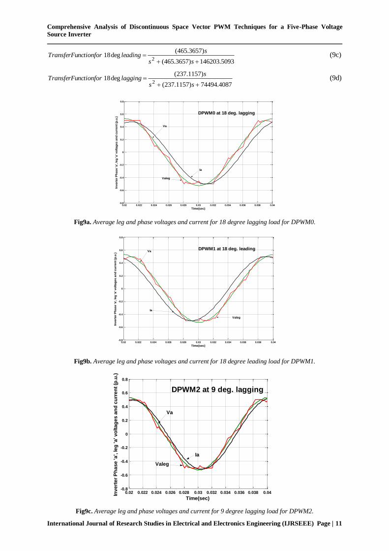
Simulation is once again carried out for different loading conditions. The load considered is standard series RLC type of load whose transfer function is given by equations (9) and the resulting average
voltage, average current and leg voltages are shown in Fig. 9.
LCsLRs
sLnctionTransferFu
/1)/(
)/1(2
(9)
Keeping R = 1 ohm and Xc = 1 ohm,
3896.117273)28119.373(
)28119.373(deg9
2
ss
sleadingnctionforTransferFu (9a)
10713.85204)204673.271(
)204673.271(deg9
2
ss
slaggingnctionforTransferFu (9b)
V1(1 1 0 0 1)
V7(0 0 111 )
V8(0 0 0 1 1) V9(1 0 0 1 1)
V10(1 0 0 0 1)
V6(0 0 1 1 0)
V5(0 1 1 1 0)
V4(0 1 1 0 0) V3(1 1 1 0 0)
V2(1 1 0 0 0)
α
β
V11(10000)
V17(00010)
V18(10111)V19(00001)
V20(11011)
V16(01111)
V15(00100)
V14(11110) V13(01000)
V12(11101)
T31 = 0
T0 = 0
T31 = 0
T0 = 0
T31 = 0
T0 = 0T31 = 0T0 = 0 T31 = 0
T0 = 0
T31 = 0
T0 = 0
T31 = 0
T0 = 0
T31 = 0
T0 = 0
T31 = 0
T0 = 0
T31 = 0
T0 = 0
V1(1 1 0 0 1)
V7(0 0 111 )
V8(0 0 0 1 1) V9(1 0 0 1 1)
V10(1 0 0 0 1)
V6(0 0 1 1 0)
V5(0 1 1 1 0)
V4(0 1 1 0 0) V3(1 1 1 0 0)
V2(1 1 0 0 0)
α
β
V11(10000)
V17(00010)
V18(10111)V19(00001)
V20(11011)
V16(01111)
V15(00100)
V14(11110) V13(01000)
V12(11101)
T31 = 0
T0 = 0
T31 = 0
T0 = 0
T31 = 0T0 = 0 T31 = 0
T0 = 0 T31 = 0
T0 = 0
T31 = 0
T0 = 0
T31 = 0
T0 = 0
T31 = 0
T0 = 0
T31 = 0
T0 = 0
T31 = 0
T0 = 0
Comprehensive Analysis of Discontinuous Space Vector PWM Techniques for a Five-Phase Voltage
Source Inverter
International Journal of Research Studies in Electrical and Electronics Engineering (IJRSEEE) Page | 11
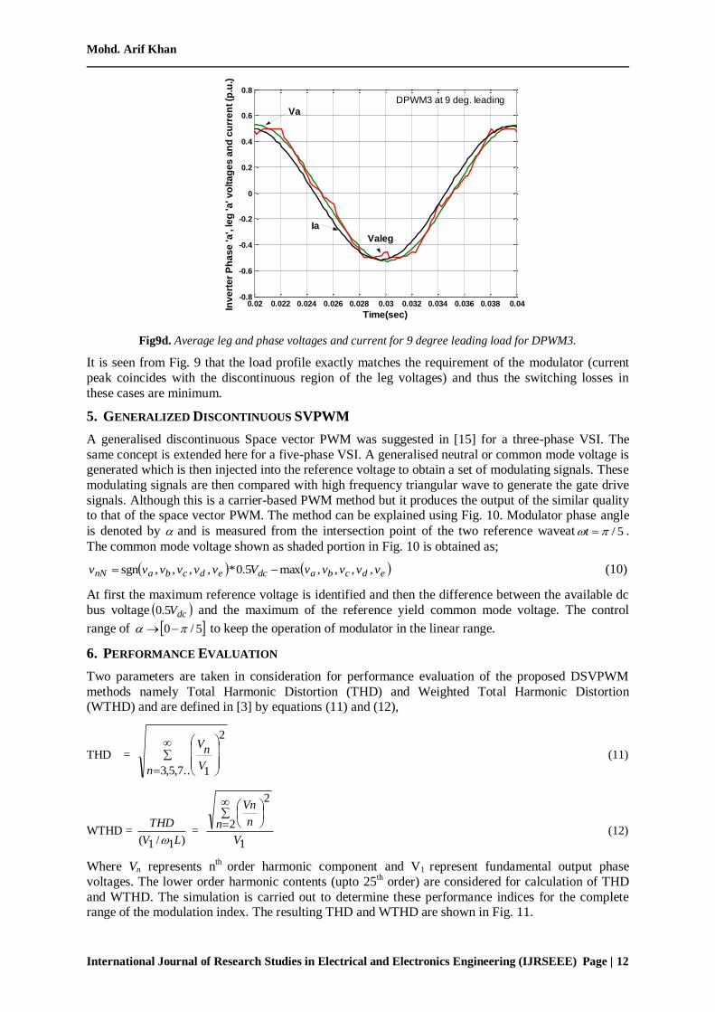
5093.146203)3657.465(
)3657.465(deg18
2
ss
sleadingnctionforTransferFu (9c)
4087.74494)1157.237(
)1157.237(deg18
2
ss
slaggingnctionforTransferFu (9d)
Fig9a. Average leg and phase voltages and current for 18 degree lagging load for DPWM0.
Fig9b. Average leg and phase voltages and current for 18 degree leading load for DPWM1.
Fig9c. Average leg and phase voltages and current for 9 degree lagging load for DPWM2.
0.02 0.022 0.024 0.026 0.028 0.03 0.032 0.034 0.036 0.038 0.04-0.8
-0.6
-0.4
-0.2
0
0.2
0.4
0.6
0.8
Time(sec)
Inv
ert
er
Ph
as
e 'a
', le
g 'a
' v
olt
ag
es
an
d c
urr
en
t (p
.u.)
Va
Valeg
Ia
DPWM0 at 18 deg. lagging
0.02 0.022 0.024 0.026 0.028 0.03 0.032 0.034 0.036 0.038 0.04-0.8
-0.6
-0.4
-0.2
0
0.2
0.4
0.6
0.8
Time(sec)
Inv
ert
er
Ph
as
e 'a
', le
g 'a
' v
olt
ag
es
an
d c
urr
en
t (p
.u.)
Va
Valeg
Ia
DPWM1 at 18 deg. leading
0.02 0.022 0.024 0.026 0.028 0.03 0.032 0.034 0.036 0.038 0.04-0.8
-0.6
-0.4
-0.2
0
0.2
0.4
0.6
0.8
Time(sec)
Inv
ert
er
Ph
as
e 'a
', le
g 'a
' v
olt
ag
es
an
d c
urr
en
t (p
.u.)
Va
Valeg
Ia
DPWM2 at 9 deg. lagging
Mohd. Arif Khan
International Journal of Research Studies in Electrical and Electronics Engineering (IJRSEEE) Page | 12
Fig9d. Average leg and phase voltages and current for 9 degree leading load for DPWM3.
It is seen from Fig. 9 that the load profile exactly matches the requirement of the modulator (current
peak coincides with the discontinuous region of the leg voltages) and thus the switching losses in
these cases are minimum.
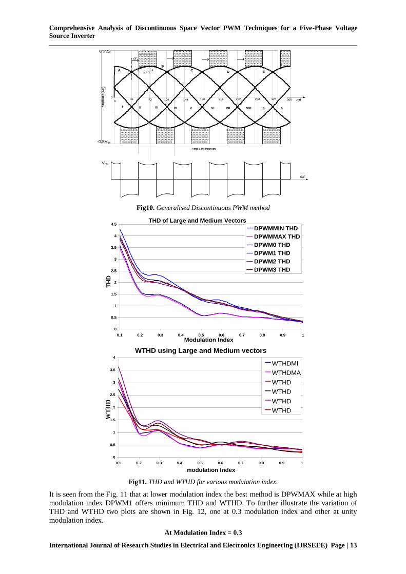
5. GENERALIZED DISCONTINUOUS SVPWM
A generalised discontinuous Space vector PWM was suggested in [15] for a three-phase VSI. The
same concept is extended here for a five-phase VSI. A generalised neutral or common mode voltage is generated which is then injected into the reference voltage to obtain a set of modulating signals. These
modulating signals are then compared with high frequency triangular wave to generate the gate drive
signals. Although this is a carrier-based PWM method but it produces the output of the similar quality to that of the space vector PWM. The method can be explained using Fig. 10. Modulator phase angle
is denoted by and is measured from the intersection point of the two reference waveat 5/ t .
The common mode voltage shown as shaded portion in Fig. 10 is obtained as;
edcbadcedcbanN vvvvvVvvvvvv ,,,,max5.0*,,,,sgn (10)
At first the maximum reference voltage is identified and then the difference between the available dc
bus voltage dcV5.0 and the maximum of the reference yield common mode voltage. The control
range of 5/0 to keep the operation of modulator in the linear range.
6. PERFORMANCE EVALUATION
Two parameters are taken in consideration for performance evaluation of the proposed DSVPWM
methods namely Total Harmonic Distortion (THD) and Weighted Total Harmonic Distortion (WTHD) and are defined in [3] by equations (11) and (12),
THD =
..7,5,3
2
1n V
nV (11)
WTHD = )1/1( LV
THD
=
1
2
2
V
n n
Vn
(12)
Where Vn represents nth
order harmonic component and V1 represent fundamental output phase
voltages. The lower order harmonic contents (upto 25th order) are considered for calculation of THD
and WTHD. The simulation is carried out to determine these performance indices for the complete range of the modulation index. The resulting THD and WTHD are shown in Fig. 11.
0.02 0.022 0.024 0.026 0.028 0.03 0.032 0.034 0.036 0.038 0.04-0.8
-0.6
-0.4
-0.2
0
0.2
0.4
0.6
0.8
Time(sec)
Inv
ert
er
Ph
as
e 'a
', le
g 'a
' v
olt
ag
es
an
d c
urr
en
t (p
.u.)
Va
Valeg
Ia
DPWM3 at 9 deg. leading
Comprehensive Analysis of Discontinuous Space Vector PWM Techniques for a Five-Phase Voltage
Source Inverter
International Journal of Research Studies in Electrical and Electronics Engineering (IJRSEEE) Page | 13
0
036 72 108 144 180 216 252 288 324 360
Angle in degrees
Am
plitu
de
(p
.u.)
I II III IV V VI VII VIII IX X
A
B
C D E
0.5Vdc
5/
-0.5Vdc
t
XX XXXXXXXXXXXXX
XXXXXXXXXXXX
XXXXXXXXXXXX
XXXXXXXXXXXX
XXXXXXXXXXXX
XXXXXXXXXX
XXXXXXXXXXXX
XXXXXXXXXXXX
XXXXXXXXXXXX
XXXXXXXXXXXX
XXXXXXXXXXXX
XXXXXXXXXXXX
XXXXXXXXXXXXXX
XXXXXXXXXXXX
XXXXXXXXXXXX
XXXXXXXXXXXX
XXXXXXXXXXXX
XXXXXXXXXXXX
XXXXXXXXXXXX
XXXXXXXXXXXXXX
XXXXXXXXXXXX
XXXXXXXXXXXX
XXXXXXXXXXXX
XXXXXXXXXXXX
XXXXXXXXXXXX
XXXXXXXXXXXX
XXXXXXXXXXXXXX
XXXXXXXXXXXX
XXXXXXXXXXXX
XXXXXXXXXXXX
XXXXXXXXXXXX
XXXXXXXXXXXX
XXXXXXXXXXXX
XXXXXXXXXXXXXX
XXXXXXXXXXXX
XXXXXXXXXXXX
XXXXXXXXXXXX
XXXXXXXXXXXX
XXXXXXXXXXXX
XXXXXXXXXX
XXXXXXXXXXXX
XXXXXXXXXXXX
XXXXXXXXXXXX
XXXXXXXXXXXX
XXXXXXXXXXXX
XXXXXXXXXX
XXXXXXXXXXXX
XXXXXXXXXXXX
XXXXXXXXXXXX
XXXXXXXXXXXX
XXXXXXXXXXXX
XXXXXXXXXX
XXXXXXXXXXXX
XXXXXXXXXXXX
XXXXXXXXXXXX
XXXXXXXXXXXX
XXXXXXXXXXXX
XXXXXXXXXX
X
X
XXXXXX
XXXXXX
XXXXXX
XXXXXX
XXXXXX
XXXXXX
XXXXXX
t
VnN
Fig10. Generalised Discontinuous PWM method
WTHD using Large and Medium vectors
0
0.5
1
1.5
2
2.5
3
3.5
4
0.1 0.2 0.3 0.4 0.5 0.6 0.7 0.8 0.9 1
modulation Index
WT
HD
WTHDMIN WTHDMAX WTHD 0 WTHD 1 WTHD 2 WTHD 3
Fig11. THD and WTHD for various modulation index.
It is seen from the Fig. 11 that at lower modulation index the best method is DPWMAX while at high
modulation index DPWM1 offers minimum THD and WTHD. To further illustrate the variation of THD and WTHD two plots are shown in Fig. 12, one at 0.3 modulation index and other at unity
modulation index.
At Modulation Index = 0.3
THD of Large and Medium Vectors
0
0.5
1
1.5
2
2.5
3
3.5
4
4.5
0.1 0.2 0.3 0.4 0.5 0.6 0.7 0.8 0.9 1
Modulation Index
TH
D
DPWMMIN THD
DPWMMAX THD
DPWM0 THD
DPWM1 THD
DPWM2 THD
DPWM3 THD
Mohd. Arif Khan
International Journal of Research Studies in Electrical and Electronics Engineering (IJRSEEE) Page | 14
At Modulation Index = 1
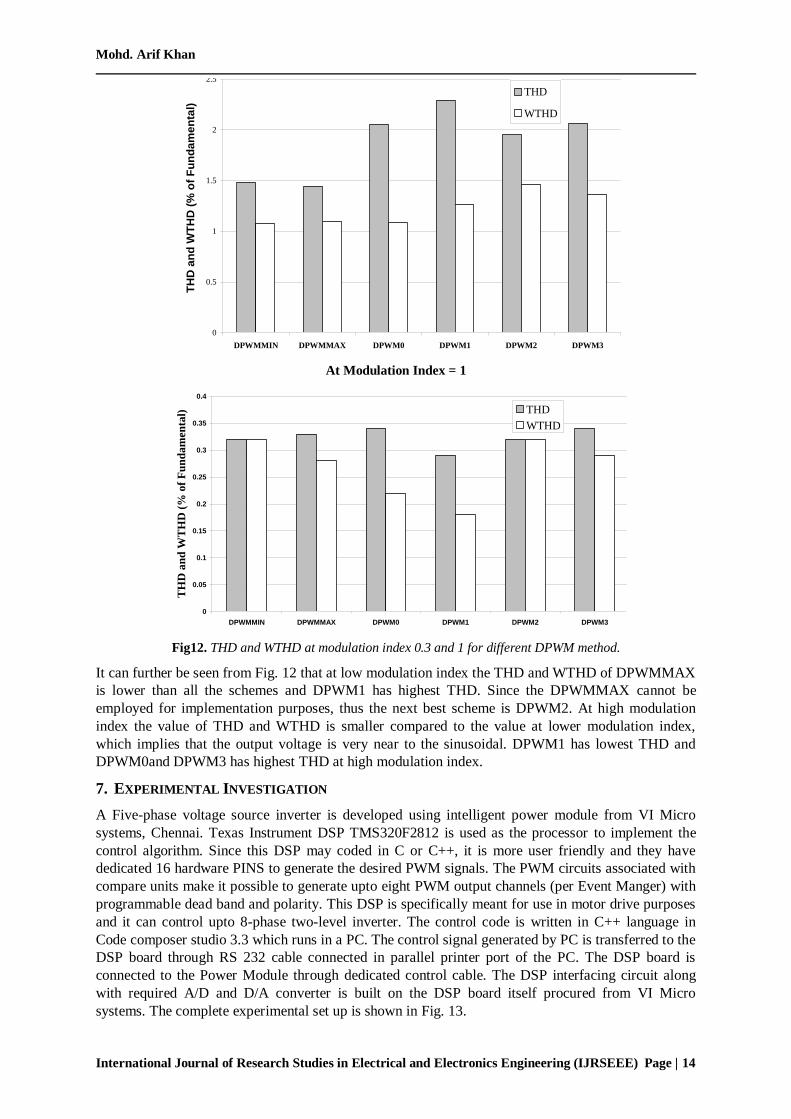
Fig12. THD and WTHD at modulation index 0.3 and 1 for different DPWM method.
It can further be seen from Fig. 12 that at low modulation index the THD and WTHD of DPWMMAX
is lower than all the schemes and DPWM1 has highest THD. Since the DPWMMAX cannot be
employed for implementation purposes, thus the next best scheme is DPWM2. At high modulation
index the value of THD and WTHD is smaller compared to the value at lower modulation index,
which implies that the output voltage is very near to the sinusoidal. DPWM1 has lowest THD and
DPWM0and DPWM3 has highest THD at high modulation index.
7. EXPERIMENTAL INVESTIGATION
A Five-phase voltage source inverter is developed using intelligent power module from VI Micro
systems, Chennai. Texas Instrument DSP TMS320F2812 is used as the processor to implement the
control algorithm. Since this DSP may coded in C or C++, it is more user friendly and they have
dedicated 16 hardware PINS to generate the desired PWM signals. The PWM circuits associated with
compare units make it possible to generate upto eight PWM output channels (per Event Manger) with
programmable dead band and polarity. This DSP is specifically meant for use in motor drive purposes
and it can control upto 8-phase two-level inverter. The control code is written in C++ language in
Code composer studio 3.3 which runs in a PC. The control signal generated by PC is transferred to the
DSP board through RS 232 cable connected in parallel printer port of the PC. The DSP board is
connected to the Power Module through dedicated control cable. The DSP interfacing circuit along
with required A/D and D/A converter is built on the DSP board itself procured from VI Micro
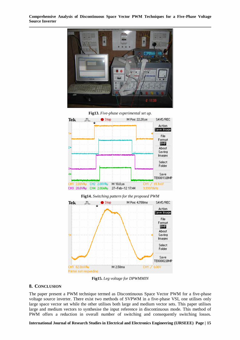
systems. The complete experimental set up is shown in Fig. 13.
At Modulation Index = 0.3
0
0.5
1
1.5
2
2.5
DPWMMIN DPWMMAX DPWM0 DPWM1 DPWM2 DPWM3
TH
D a
nd
WT
HD
(%
of
Fu
nd
am
en
tal)
THD
WTHD
At modulation Index = 1
0
0.05
0.1
0.15
0.2
0.25
0.3
0.35
0.4
DPWMMIN DPWMMAX DPWM0 DPWM1 DPWM2 DPWM3
TH
D a
nd
WT
HD
(%
of
Fu
nd
am
enta
l) THD
WTHD
Comprehensive Analysis of Discontinuous Space Vector PWM Techniques for a Five-Phase Voltage
Source Inverter
International Journal of Research Studies in Electrical and Electronics Engineering (IJRSEEE) Page | 15
Fig13. Five-phase experimental set up.
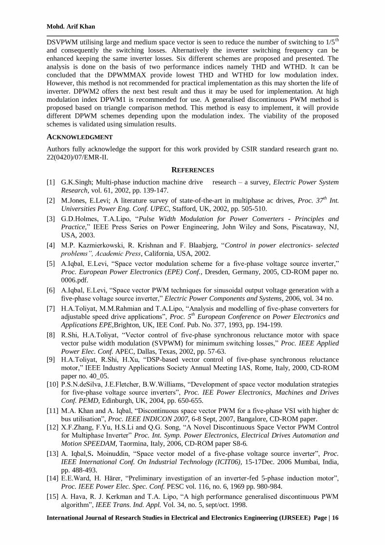
Fig14. Switching pattern for the proposed PWM
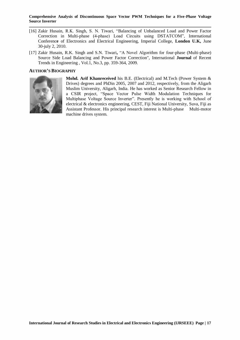
Fig15. Leg voltage for DPWMMIN
8. CONCLUSION
The paper present a PWM technique termed as Discontinuous Space Vector PWM for a five-phase voltage source inverter. There exist two methods of SVPWM in a five-phase VSI, one utilises only
large space vector set while the other utilises both large and medium vector sets. This paper utilises
large and medium vectors to synthesise the input reference in discontinuous mode. This method of PWM offers a reduction in overall number of switching and consequently switching losses.
Mohd. Arif Khan
International Journal of Research Studies in Electrical and Electronics Engineering (IJRSEEE) Page | 16
DSVPWM utilising large and medium space vector is seen to reduce the number of switching to 1/5th
and consequently the switching losses. Alternatively the inverter switching frequency can be
enhanced keeping the same inverter losses. Six different schemes are proposed and presented. The
analysis is done on the basis of two performance indices namely THD and WTHD. It can be
concluded that the DPWMMAX provide lowest THD and WTHD for low modulation index. However, this method is not recommended for practical implementation as this may shorten the life of
inverter. DPWM2 offers the next best result and thus it may be used for implementation. At high
modulation index DPWM1 is recommended for use. A generalised discontinuous PWM method is proposed based on triangle comparison method. This method is easy to implement, it will provide
different DPWM schemes depending upon the modulation index. The viability of the proposed
schemes is validated using simulation results.
ACKNOWLEDGMENT
Authors fully acknowledge the support for this work provided by CSIR standard research grant no.
22(0420)/07/EMR-II.
REFERENCES
[1] G.K.Singh; Multi-phase induction machine drive research – a survey, Electric Power System
Research, vol. 61, 2002, pp. 139-147.
[2] M.Jones, E.Levi; A literature survey of state-of-the-art in multiphase ac drives, Proc. 37th Int.
Universities Power Eng. Conf. UPEC, Stafford, UK, 2002, pp. 505-510.
[3] G.D.Holmes, T.A.Lipo, “Pulse Width Modulation for Power Converters - Principles and Practice,” IEEE Press Series on Power Engineering, John Wiley and Sons, Piscataway, NJ,
USA, 2003.
[4] M.P. Kazmierkowski, R. Krishnan and F. Blaabjerg, “Control in power electronics- selected
problems”, Academic Press, California, USA, 2002.
[5] A.Iqbal, E.Levi, “Space vector modulation scheme for a five-phase voltage source inverter,”
Proc. European Power Electronics (EPE) Conf., Dresden, Germany, 2005, CD-ROM paper no.
0006.pdf.
[6] A.Iqbal, E.Levi, “Space vector PWM techniques for sinusoidal output voltage generation with a
five-phase voltage source inverter,” Electric Power Components and Systems, 2006, vol. 34 no.
[7] H.A.Toliyat, M.M.Rahmian and T.A.Lipo, “Analysis and modelling of five-phase converters for adjustable speed drive applications”, Proc. 5
th European Conference on Power Electronics and
Applications EPE,Brighton, UK, IEE Conf. Pub. No. 377, 1993, pp. 194-199.
[8] R.Shi, H.A.Toliyat, “Vector control of five-phase synchronous reluctance motor with space
vector pulse width modulation (SVPWM) for minimum switching losses,” Proc. IEEE Applied
Power Elec. Conf. APEC, Dallas, Texas, 2002, pp. 57-63. [9] H.A.Toliyat, R.Shi, H.Xu, “DSP-based vector control of five-phase synchronous reluctance
motor,” IEEE Industry Applications Society Annual Meeting IAS, Rome, Italy, 2000, CD-ROM
paper no. 40_05.
[10] P.S.N.deSilva, J.E.Fletcher, B.W.Williams, “Development of space vector modulation strategies for five-phase voltage source inverters”, Proc. IEE Power Electronics, Machines and Drives
Conf. PEMD, Edinburgh, UK, 2004, pp. 650-655.
[11] M.A. Khan and A. Iqbal, “Discontinuous space vector PWM for a five-phase VSI with higher dc
bus utilisation”, Proc. IEEE INDICON 2007, 6-8 Sept, 2007, Bangalore, CD-ROM paper.
[12] X.F.Zhang, F.Yu, H.S.Li and Q.G. Song, “A Novel Discontinuous Space Vector PWM Control for Multiphase Inverter” Proc. Int. Symp. Power Electronics, Electrical Drives Automation and
Motion SPEEDAM, Taormina, Italy, 2006, CD-ROM paper S8-6.
[13] A. Iqbal,S. Moinuddin, “Space vector model of a five-phase voltage source inverter”, Proc.
IEEE International Conf. On Industrial Technology (ICIT06), 15-17Dec. 2006 Mumbai, India,
pp. 488-493. [14] E.E.Ward, H. Härer, “Preliminary investigation of an inverter-fed 5-phase induction motor”,
Proc. IEEE Power Elec. Spec. Conf. PESC vol. 116, no. 6, 1969 pp. 980-984.
[15] A. Hava, R. J. Kerkman and T.A. Lipo, “A high performance generalised discontinuous PWM
algorithm”, IEEE Trans. Ind. Appl. Vol. 34, no. 5, sept/oct. 1998.
Comprehensive Analysis of Discontinuous Space Vector PWM Techniques for a Five-Phase Voltage
Source Inverter
International Journal of Research Studies in Electrical and Electronics Engineering (IJRSEEE) Page | 17
[16] Zakir Husain, R.K. Singh, S. N. Tiwari, “Balancing of Unbalanced Load and Power Factor Correction in Multi-phase (4-phase) Load Circuits using DSTATCOM”, International
Conference of Electronics and Electrical Engineering, Imperial College, London U.K, June
30-july 2, 2010.
[17] Zakir Husain, R.K. Singh and S.N. Tiwari, “A Novel Algorithm for four-phase (Multi-phase)
Source Side Load Balancing and Power Factor Correction", International Journal of Recent Trends in Engineering , Vol.1, No.3, pp. 359-364, 2009.
AUTHOR’S BIOGRAPHY
Mohd. Arif Khanreceived his B.E. (Electrical) and M.Tech (Power System & Drives) degrees and PhDin 2005, 2007 and 2012, respectively, from the Aligarh
Muslim University, Aligarh, India. He has worked as Senior Research Fellow in
a CSIR project, “Space Vector Pulse Width Modulation Techniques for Multiphase Voltage Source Inverter”. Presently he is working with School of
electrical & electronics engineering, CEST, Fiji National University, Suva, Fiji as
Assistant Professor. His principal research interest is Multi-phase Multi-motor
machine drives system.