Embed Size (px)
Citation preview
Computational Analysis of CantileverBeam Electrostatic MEMS Actuators
A project report submitted in partial fulfillment of the requirements for thedegree of
Master of Technology
in
Computational Science
by
Girish Sathyanarayana
Supercomputer Education and Research Center
Indian Institute of Science
Bangalore - 560012
June - 2010

ACKNOWLEDGEMENT
I owe most of the project to my adviser Prof. A Mohanty who has conceivedthe project and guided me at every step. it was a great privilege workingwith him. aided with his guidance, I could complete the project withoutmuch trouble and it was a really smooth ride. I take this opportunity toexpress my profound gratitude to him.I thank Prof. Govindrajan, chairman, SERC who has always been very mo-tivating.I thank the faculty members of IISc who through their courses helped melearn many things.I also thank my colleagues Jitender, Raju and Susil for sharing some nicemoments during my stay in IISc.I thank my parents and all my family members for always being very sup-portive.Finally, I thank government of India and people of the country for the schol-arship.
i
Abstract
The objective of this project is to computationally analyse thebehaviour of MEMS parallel plate actuators under the influence ofelectro-static stresses.The problem is the following :When an external voltage is applied to a parallel-plate actuator, elec-trostatic charges are induced on the surface of the conductors. positivecharges on the conductor held at higher potential and negative chargeson the other conductor. the charge distribution depends on the geom-etry of the configuration.The induced charges give rise to electrostatic forces which can deformone of the conductors(other conductor being fixed cannot deform).when the conductor deforms, the charges redistribute thereby chang-ing the electrostatic forces. Now, the conductor deforms again consis-tent with the new force.This process of deformation continues until the deformations no longerchanges the forces significantly, successive deformations becomes moreand more small and we may say that the system has reached its equi-librium position. or the deformations can become large enough so thatthe deformed conductor touches the fixed conductor, when we say aPull-in has occured.For the purpose of computational analysis, the problem can be splitup into two parts.1. finding the charge distribution, given the geometry.2. finding the deformation, given the charge distribution.Starting from an initial undeformed configuration, the above problemsare solved alternatively until one of the end-state(an equilibrium po-sition or a pull-in) is reached.Approach taken is the following :Boundary Element Method to find the charge distributionA Finite Difference scheme to find the deformation using a 1-D BeamModel for the conductor.
ii
Contents
1 Introduction 1
2 Electrical Analysis by Boundary Element method 5
3 Mechanical Analysis by using 1D beam model 20
4 Results and Validation 30
5 Conclusion 45
6 Appendix 46
7 References 50
iii
LIST OF FIGURES
Fig. 1.1 : Bending of parallel plate actuators under the influence of electro-static stresses . . . . . . . . . . . . . . . . . . . . . . . . . . . . . . . . . . . . . . . . . . . . . . . . . . . . . . . . . . . 1Fig. 2.1 : A conductor of arbitrary shape defined by closed region S . . . . . 5Fig. 2.2 : A panelized rectangular strip held at V volts . . . . . . . . . . . . . . . . . 8Fig. 2.3 : Potential due to uniform charge distribution on a rectangle at itscentroid . . . . . . . . . . . . . . . . . . . . . . . . . . . . . . . . . . . . . . . . . . . . . . . . . . . . . . . . . . . . . . . 10Fig. 2.4 : Difference between periodic and aperiodic surface . . . . . . . . . . . . 16Fig. 2.5 : Data structure encapsulating the system information . . . . . . . . 18Fig. 3.1 : Force between panels . . . . . . . . . . . . . . . . . . . . . . . . . . . . . . . . . . . . . . . . 20Fig. 3.2 : Combining point forces to find the distributed loads . . . . . . . . . 23Fig. 3.3 : Discretization of 1D domain of solution . . . . . . . . . . . . . . . . . . . . . . 24Fig. 4.1 : Charge distribution on a 1× 0.5mm rectangular strip held at 10V31Fig. 4.2 : Charge distribution on parallel plates each of dimension 1×0.5mm, upper plate held at 10V and lower plate at 0V . . . . . . . . . . . . . . . . . . . . . . . 32Fig. 4.3 : Charge distribution on parallel plates, distance between them be-ing negligibly small compared to plate dimensions . . . . . . . . . . . . . . . . . . . . . 33Fig. 4.4 : Charge distribution on parallel plates held at opposite voltages .34Fig. 4.5 : Graph of induced charge v/s distance from center on a disc . . 35Fig. 4.6 : Comparison between analytical and theoretical results for the caseof point load at free end . . . . . . . . . . . . . . . . . . . . . . . . . . . . . . . . . . . . . . . . . . . . . . . 37Fig. 4.7 : Comparison between analytical and theoretical results for the caseof point load at the center of the beam . . . . . . . . . . . . . . . . . . . . . . . . . . . . . . . . 38Fig. 4.8 : Equilibrium states for different voltages for configuration 1 . . 40Fig. 4.9 : Deflection at pull-in for configuration 1 . . . . . . . . . . . . . . . . . . . . . . 41Fig. 4.10 : Equilibrium states for different voltages for configuration 2 . 42Fig. 4.11 : Deflection at pull-in for configuration 2 . . . . . . . . . . . . . . . . . . . . . 43Fig. 6.1 : Potential due to uniform charge distribution on a right angledtriangle . . . . . . . . . . . . . . . . . . . . . . . . . . . . . . . . . . . . . . . . . . . . . . . . . . . . . . . . . . . . . . . . 46
iv
1 Introduction
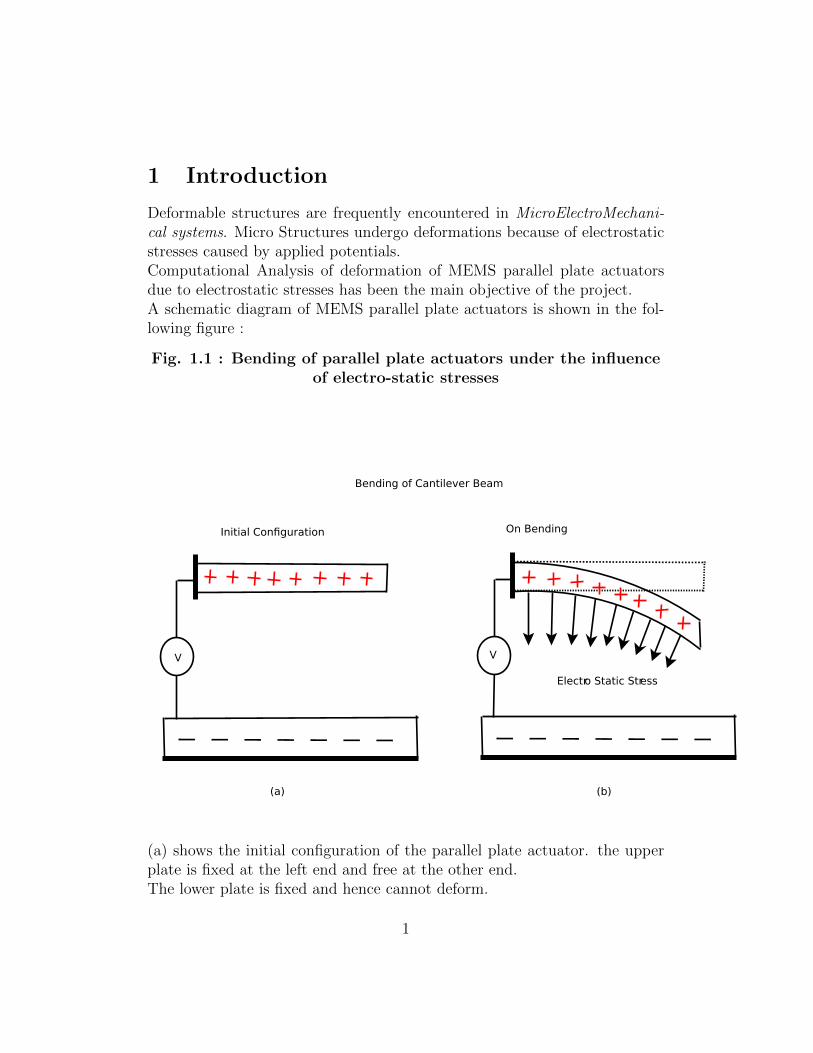
Deformable structures are frequently encountered in MicroElectroMechani-cal systems. Micro Structures undergo deformations because of electrostaticstresses caused by applied potentials.Computational Analysis of deformation of MEMS parallel plate actuatorsdue to electrostatic stresses has been the main objective of the project.A schematic diagram of MEMS parallel plate actuators is shown in the fol-lowing figure :
Fig. 1.1 : Bending of parallel plate actuators under the influenceof electro-static stresses
V V
(a) (b)
Initial Configuration
Bending of Cantilever Beam
Electro Static Stress
On Bending
(a) shows the initial configuration of the parallel plate actuator. the upperplate is fixed at the left end and free at the other end.The lower plate is fixed and hence cannot deform.
1
The upper plate is held at a voltage V with respect to the fixed plate.positivecharges are induced on the upper plate and negative charges on the fixedplate. this results in an attractive force between the two plates.(b) shows upper plate getting deformed due to electrostatic stresses.
As seen in Fig. 1.1, when a voltage is applied, static charges are inducedon the surfaces the plates.The upper plate is held at a positive voltage. hence the charges induced onthe upper plate will be positive so as to keep the voltage at any point on theupper plate equal to applied voltage V ( conductor surface is an equipotentialsurface).The fixed plate is held at zero potential. Now, the positive charges on theupper plate will result in positive potentials at the surface of the fixed plate.hence, negative charges will be induced on the surface of the fixed plate so asto nullify the positive potentials due to positive charges on the upper plateand maintain any point on the fixed plate at zero potential.On the whole, the effect of applying an external voltage to our system isto induce positive charges on the upper plate and negative charges on thefixed plate. the distribution of these charges depends on applied voltage andgeometry of the system(“geometry of the system” refers to parameters likedimensions of the plate, distance between plates etc. in general, the term“change in geometry” is used to imply deflection of the upper plate fromcurrent position to a new position) .The opposite polarity charges on the plates gives rise to attractive forcesbetween the plates. the lower plane being fixed cannot deform. the upperplate is fixed at left end and free at the other end. it deflects according tomechanical properties of the material used for plates.When the upper plate deflects, the geometry changes and as explained abovethe charge distribution changes consequently. thus, the forces also changeand therefore the plate cannot remain at the current(deflected)position. thenew force will have a corresponding deflection relative to initial configurationand the plate will make a transition to this position.This position is not stable as well. for the same reasons as before the plateagain deflects to a new position and this process continues and can have twopossible end states.
2
1. The successive changes in deflection becomes smaller and smaller andfurther deflections become negligible. we may refer to this state asequilibrium position.
2. the deflection becomes large enough so that the upper plate touchesthe fixed plate. this state is referred as Pull-in.
For the sake computational analysis, the problem logically splits up intotwo parts.
• How to find the charges given the geometry.
• How to find the deflection given the charges.
If we can solve the above two problems, we can use the following algo-rithm which completely determines the end state of our parallel plate system.
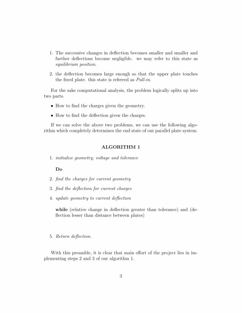
ALGORITHM 1
1. initialize geometry, voltage and tolerance
Do
2. find the charges for current geometry
3. find the deflection for current charges
4. update geometry to current deflection
while (relative change in deflection greater than tolerance) and (de-flection lesser than distance between plates)
5. Return deflection.
With this preamble, it is clear that main effort of the project lies in im-plementing steps 2 and 3 of our algorithm 1.
3

Approach used is the following :
Electrical Analysis by boundary element method to solve for charges giventhe geometry.Mechanical Analysis by a finite difference scheme using a 1D Beam modelfor the upper plate to determine deflections.
In the rest of the thesis, I shall give a brief account of these methodsand results obtained by applying these methods to implement algorithm 1.I shall also give a brief account of various implementational details involved.
4
2 Electrical Analysis by Boundary Element
method
As seen in the previous section, the main effort of the project lies in imple-menting steps 2 and 3 of algorithm 1 .In this section, I shall explain details involved in implementing the step 2.i.e. how to find the charges given the geometry?
The approach taken is that of solving the following general problem :given some arbitrary layout of conductors, with geometry specified and heldat different voltages, solve for charge distribution on the conductors.If we can solve this general problem, the problem of charge distribution ofour parallel plate system is solved as one of the special cases.
The problem is solved by using boundary element method.
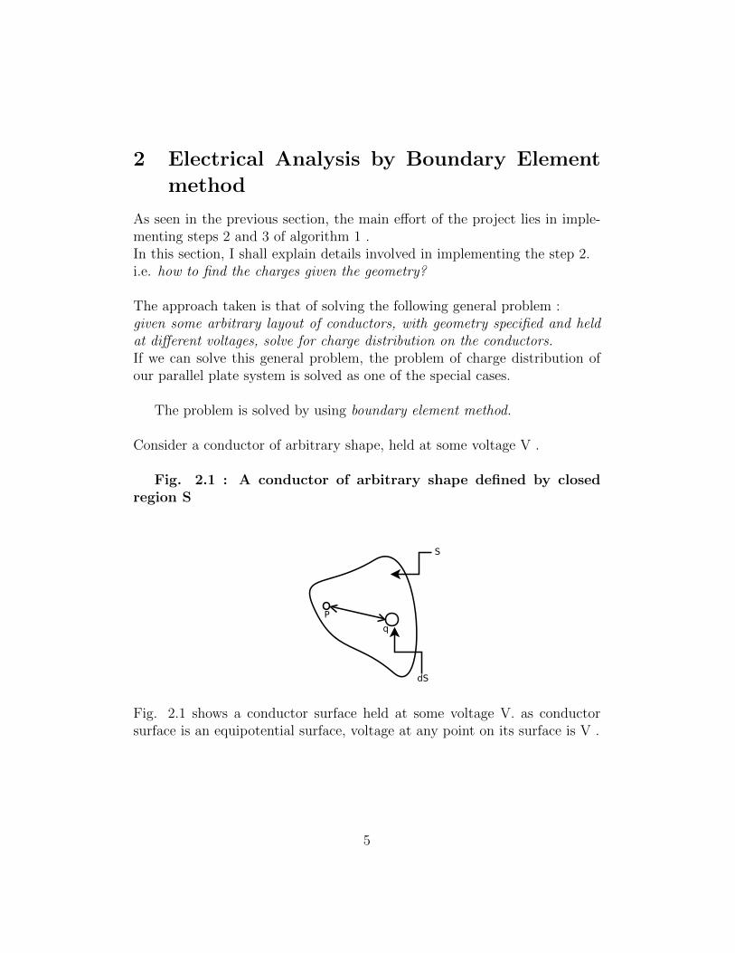
Consider a conductor of arbitrary shape, held at some voltage V .
Fig. 2.1 : A conductor of arbitrary shape defined by closedregion S
P
q
dS
S
Fig. 2.1 shows a conductor surface held at some voltage V. as conductorsurface is an equipotential surface, voltage at any point on its surface is V .
5
In reference to Fig. 2.1, we can write the boundary-integral expressionfor voltage at some point P on its surface as following :
V (P ) =
∫S
G(P, q)σ(q) dS (2.1)
whereP is the source point.q is the field point.dS is the differential region enclosing the field point q.V (P ) : voltage at point P .σ is the unknown surface charge density.G is the green’s function.
Boundary element method is used to solve for unknown surface charge dis-tribution in the boundary integral formulation given by equation 2.1.In this method, the surface is discretized into panels and the surface chargedensity is assumed to be constant on each panel. the centroid is taken as thecollocation point and the value of the potential and surface charge densityat the collocation point represent the value of potential and surface chargedensity on the panel.The boundary integral expression for a source point P can now be writtenas following :
V (P ) =n∑i=1
∫Si
G(P, qi)σi dSi (2.2)
wheren is the number of panels.V (P ) is the voltage of the Pth panel.qi is a field point inside panel i.dSi is the differential region enclosing the field point qi.Si is the region enclosed by ith panel .σi is the charge density on ith panel.
as σi is constant, it can be taken out of the integral.i.e. the equation can be written as
V (P ) =n∑i=1
σi
∫Si
G(P, qi) dSi (2.3)
P = 1,...,n
or
n∑i=1
[∫Si
G(P, qi) dSi
]σi = V (P ) (2.4)
P = 1,...,nequation 2.4 gives a set of n linear equations in n unknowns, which can besolved to find unknown σis.
It can be written in matrix form as follows:
M σ̄ = v̄ (2.5)
whereM ∈ Rn×n : coefficient matrixσ̄, v̄ ∈ Rn×1
M(i, j) =∫SjG(Ci, qj) dSj
Ci is the centroid of ith panel .qj is any point on the jth panel.Sj is the region occupied by the jth panel.
σ̄ =
σ1...σn
v̄ =
V...V
The problem with the above method is evaluating the integral
∫SjG(Ci, qj) dSj
to find the entries of the co-efficient matrix for different geometries.greens function takes the following form :
G(p, q) =1
4πε|p− q|(2.6)
Where |p− q| denotes the distance between points p and q.It is difficult to find a closed form expression for the above mentioned integraland the integral will have to be numerically evaluated.
7
Instead we can use the following assumption, which greatly simplifies ourproblem :For sufficiently small panels, the effect of uniform charge distribution on thesurface of the panel can be replaced by the effect of an equivalent pointcharge placed at the centroid of the panel. the equivalent charge is taken asthe total charge on the panel.We solve for these equivalent point charges at the centroid of the panels. thiscan be easily done as there is a closed form expression for potential due apoint charge.However there is one problem with this approach:The uniform charge distribution on the panel will contribute to potential atthe centroid of the panel. this charge distribution has been replaced by anequivalent point charge at the centroid. if we use this point charge to findthe contribution of the charges on panel to potential at the centroid of thepanel, we will get a singularity.The problem is easily circumvented by deriving a closed form expression forpotential at the centroid due to a uniform charge distribution on the panel.i.e. we use this expression to find the contribution of the charges on the samepanel and for all other panels, we use the equivalent point charge model.
This method can be applied to any arbitrary layout of conductors whichcan be panelized and whose geometries are mathematically tractable.
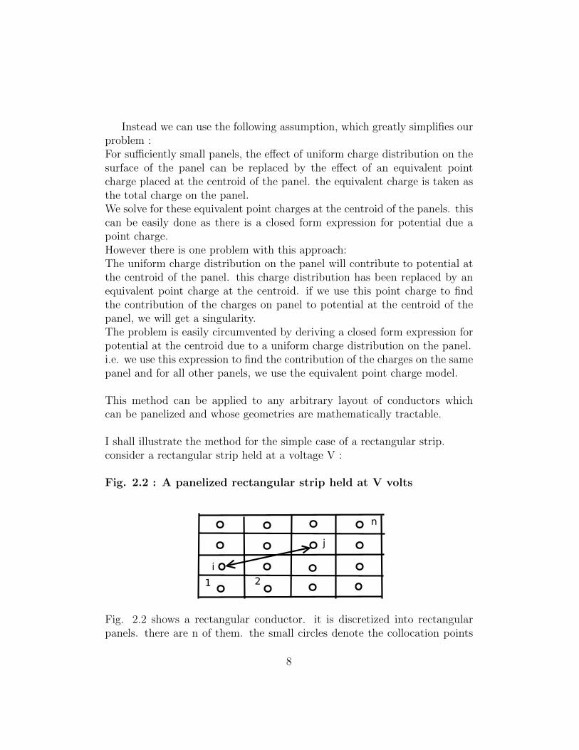
I shall illustrate the method for the simple case of a rectangular strip.consider a rectangular strip held at a voltage V :
Fig. 2.2 : A panelized rectangular strip held at V volts
i
j
1 2
n
Fig. 2.2 shows a rectangular conductor. it is discretized into rectangularpanels. there are n of them. the small circles denote the collocation points
8
which are the centroids of the panels.Equivalent charge on the centroid of the ith panel is denoted by qi, which isalso the total charge on the panel.Distance between ith and jth panel is denoted by rij.Any point on the surface of the conductor is at potential V .
Let Vi denote the potential at the centroid of ith panel and vij denote thecontribution of charges on jth panel to potential at the centroid of ith panel.It is easy to see that :
Vi =n∑j=1
vij (2.7)
As conductor surface is equipotential ,
Vi = V i = 1, ..., n (2.8)
Expression for vij for i 6= j can be written by using the expression for poten-tial due to a point charge as follows.
vij =qj
4πεoriji 6= j (2.9)
We need an expression for vii, that is the contribution of charges on the panelto potential at its centroid.We can derive an expression for potential at the centroid of a rectangle dueto uniform charge distribution as following :First, we derive an expression for potential due to a uniform charge distribu-tion on the surface of a right angled triangle at a point at some height fromone of vertices(not right angled vertex).
The following figure illustrates the method.
9
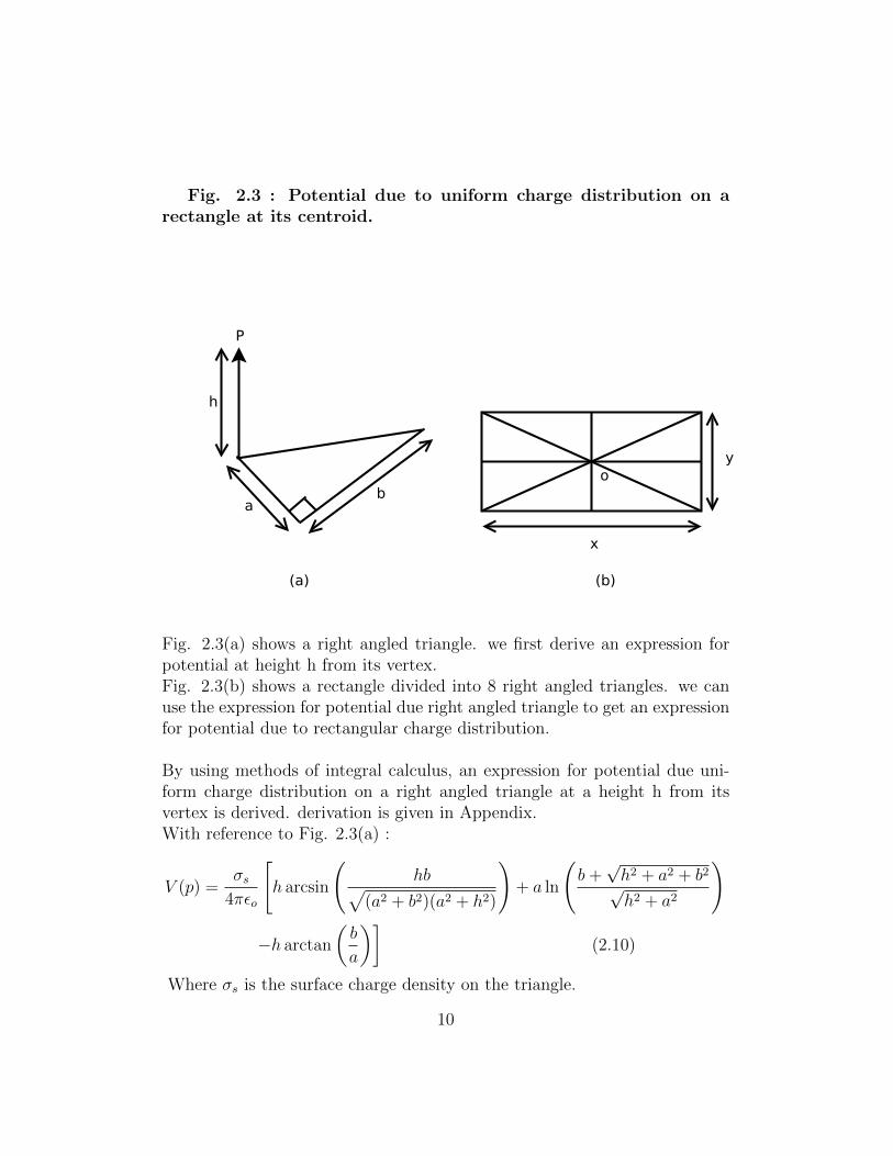
Fig. 2.3 : Potential due to uniform charge distribution on arectangle at its centroid.
ab
h
P
x
yo
(a) (b)
Fig. 2.3(a) shows a right angled triangle. we first derive an expression forpotential at height h from its vertex.Fig. 2.3(b) shows a rectangle divided into 8 right angled triangles. we canuse the expression for potential due right angled triangle to get an expressionfor potential due to rectangular charge distribution.
By using methods of integral calculus, an expression for potential due uni-form charge distribution on a right angled triangle at a height h from itsvertex is derived. derivation is given in Appendix.With reference to Fig. 2.3(a) :
V (p) =σs
4πεo
[h arcsin
(hb√
(a2 + b2)(a2 + h2)
)+ a ln
(b+√h2 + a2 + b2√h2 + a2
)
−h arctan
(b
a
)](2.10)
Where σs is the surface charge density on the triangle.
10
As we can see in Fig. 2.3(b), we can divide a rectangle into 8 right an-gled triangles and to find the potential at the centroid, we just add up thepotentials due individual right angled triangles as given by (2.10) evaluatedat height h = 0.The resulting expression is the following.With reference to Fig. 2.3(b) :
V (o) =2σs4πε0
[x ln
(y +
√x2 + y2
x
)+ y ln
(x+
√x2 + y2
y
)](2.11)
Where σs is the surface charge density on the rectangle.
Now, if the total charge on the rectangle is Q, we can replace σs by (Q/xy).now the expression will be :
V (o) =2Q
4πε0
[1
yln
(y +
√x2 + y2
x
)+
1
xln
(x+
√x2 + y2
y
)](2.12)
Using expression (2.12), we can now write the expression for vij, i.e. contri-bution of charges on the jth panel to potential at the centroid of ith panelas following :
vij =
qj
4πεoriji 6= j
2qi4πε0
[1yi
ln
(yi+√x2i+y
2i
xi
)+ 1
xiln
(xi+√x2i+y
2i
yi
)]i = j
(2.13)
Whereqi is the equivalent point charge at the centroid of the ith panel.rij is the euclidean distance between the centroids of ith and jth panel.xi and yi are the dimensions of ith panel.
substituting (2.13) in (2.7), we get
Vi =2qi
4πε0
[1
yiln
(yi +
√x2i + y2ixi
)+
1
xiln
(xi +
√x2i + y2iyi
)]+
n∑j=1,j 6=i
qj4πεorij
(2.14)i=1, ..., n.
11
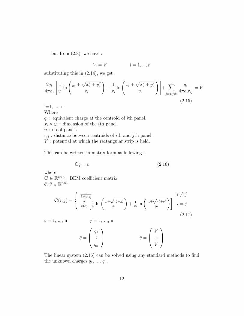
but from (2.8), we have :
Vi = V i = 1, ..., n
substituting this in (2.14), we get :
2qi4πε0
[1
yiln
(yi +
√x2i + y2ixi
)+
1
xiln
(xi +
√x2i + y2iyi
)]+
n∑j=1,j 6=i
qj4πεorij
= V
(2.15)i=1, ..., nWhereqi : equivalent charge at the centroid of ith panel.xi × yi : dimension of the ith panel.n : no of panelsrij : distance between centroids of ith and jth panel.V : potential at which the rectangular strip is held.
This can be written in matrix form as following :
Cq̄ = v̄ (2.16)
whereC ∈ Rn×n : BEM coefficient matrixq̄, v̄ ∈ Rn×1
C(i, j) =
1
4πεoriji 6= j
24πε0
[1yi
ln
(yi+√x2i+y
2i
xi
)+ 1
xiln
(xi+√x2i+y
2i
yi
)]i = j
(2.17)i = 1, ..., n j = 1, ..., n
q̄ =
q1...qn
v̄ =
V...V
The linear system (2.16) can be solved using any standard methods to findthe unknown charges q1, ..., qn.
12
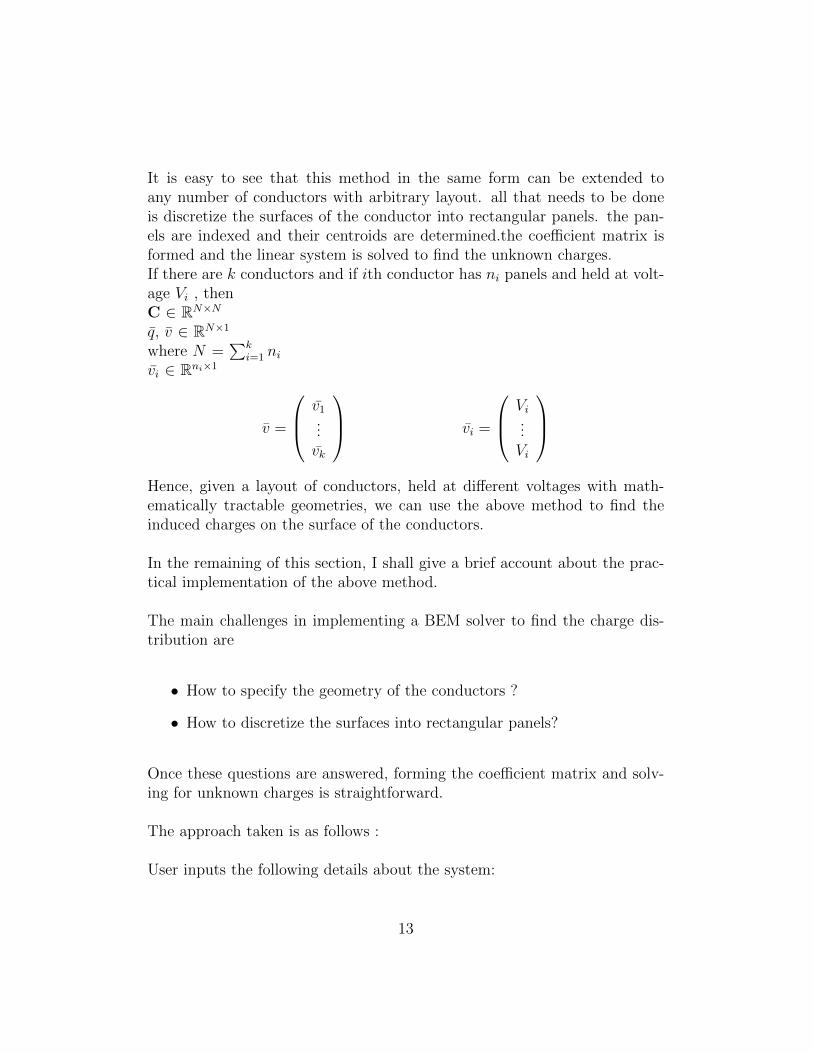
It is easy to see that this method in the same form can be extended toany number of conductors with arbitrary layout. all that needs to be doneis discretize the surfaces of the conductor into rectangular panels. the pan-els are indexed and their centroids are determined.the coefficient matrix isformed and the linear system is solved to find the unknown charges.If there are k conductors and if ith conductor has ni panels and held at volt-age Vi , thenC ∈ RN×N
q̄, v̄ ∈ RN×1
where N =∑k
i=1 niv̄i ∈ Rni×1
v̄ =
v̄1...v̄k
v̄i =
Vi...Vi
Hence, given a layout of conductors, held at different voltages with math-ematically tractable geometries, we can use the above method to find theinduced charges on the surface of the conductors.
In the remaining of this section, I shall give a brief account about the prac-tical implementation of the above method.
The main challenges in implementing a BEM solver to find the charge dis-tribution are
• How to specify the geometry of the conductors ?
• How to discretize the surfaces into rectangular panels?
Once these questions are answered, forming the coefficient matrix and solv-ing for unknown charges is straightforward.
The approach taken is as follows :
User inputs the following details about the system:
13
1. number of conductors.
2. potentials at which different conductors are held.
3. number of surfaces forming each conductor(ex: A cube has 6 surfaces).
4. parametric expression for each surface of every conductor.
• associated range of parameters.
A parametric expression for a surface defines any point on the surface interms of 2 parameters, say t1 and t2.i.e. any point on the surface can be defined by a parametric expression asfollows :
x = fx(t1, t2)y = fy(t1, t2)z = fz(t1, t2)
(2.18)
For example, any point on the surface of a unit sphere centered at origin canbe specified by a suitable value for t1 and t2 as follows :
x = sin(t1) cos(t2)y = sin(t1) sin(t2)z = cos(t1)
(2.19)
User inputs fx, fy, fz, minimum and maximum values of t1 and t2 : t1min,t1max and t2min, t2max.
Most of the simple geometries can be represented by such a scheme andby properly specifying the ranges of parameters, we can cover the desiredportion of the surface.Ex. : by choosing t1min = 0.0, t1max = π/2, t2min = 0.0 and t2max = 2πin (2.19), we can generate points covering the upper hemisphere of a unitsphere centered at origin.Parameters t1 and t2 are varied in their respective ranges and the user canfurther specify the number of times the parameters are sampled betweentheir minimum and maximum values. let it be n1 and n2.i.e.t1 is sampled n1 times between t1min and t1max.
14
t2 is sampled n2 times between t2min and t2max.We get n1 × n2 points covering the desired portion of the surface defined byfx, fy, fz.
The following algorithm sums up the method for generating the surface.
ALGORITHM 2
1. initialize fx, fy, fz, t1min, t1max, t2min, t2max, n1 and n2
for i = 0 : n1 − 1 (outer for loop)for j = 0 : n2 − 1 (inner for loop)
2. k = j + (i× n2)
3. t1eff = t1min + (t1max−t1min)in1
4. t2eff = t2min + (t2max−t2min)jn2
5. points(k) = (fx(t1eff , t2eff ), fy(t1eff , t2eff ), fz(t1eff , t2eff ))End inner for loopEnd outer for loop
6. Return points
Algorithm 2 describes the method to generate a surface. in effect wegenerate points on the surface covering the desired portion.The next task is to discretize the surface. a simple discretization method isadopted.Most of simple geometrical surfaces fall into 2 general categories:
• Periodic
• Aperiodic
15
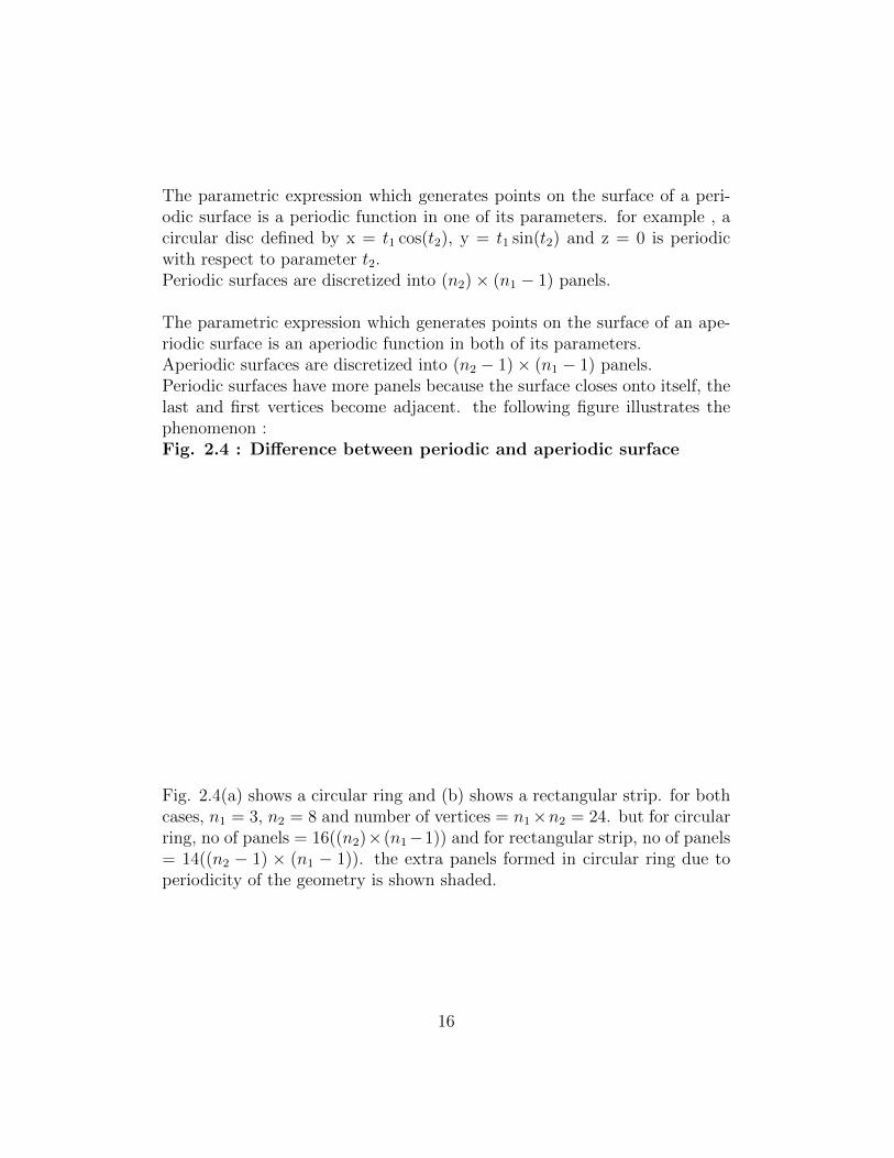
The parametric expression which generates points on the surface of a peri-odic surface is a periodic function in one of its parameters. for example , acircular disc defined by x = t1 cos(t2), y = t1 sin(t2) and z = 0 is periodicwith respect to parameter t2.Periodic surfaces are discretized into (n2)× (n1 − 1) panels.
The parametric expression which generates points on the surface of an ape-riodic surface is an aperiodic function in both of its parameters.Aperiodic surfaces are discretized into (n2 − 1)× (n1 − 1) panels.Periodic surfaces have more panels because the surface closes onto itself, thelast and first vertices become adjacent. the following figure illustrates thephenomenon :Fig. 2.4 : Difference between periodic and aperiodic surface
Fig. 2.4(a) shows a circular ring and (b) shows a rectangular strip. for bothcases, n1 = 3, n2 = 8 and number of vertices = n1×n2 = 24. but for circularring, no of panels = 16((n2)×(n1−1)) and for rectangular strip, no of panels= 14((n2 − 1) × (n1 − 1)). the extra panels formed in circular ring due toperiodicity of the geometry is shown shaded.
16
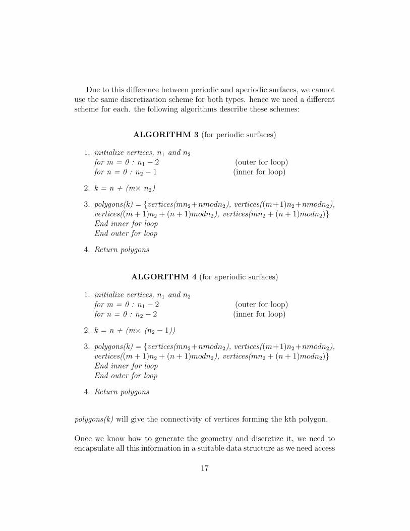
Due to this difference between periodic and aperiodic surfaces, we cannotuse the same discretization scheme for both types. hence we need a differentscheme for each. the following algorithms describe these schemes:
ALGORITHM 3 (for periodic surfaces)
1. initialize vertices, n1 and n2
for m = 0 : n1 − 2 (outer for loop)for n = 0 : n2 − 1 (inner for loop)
2. k = n + (m× n2)
3. polygons(k) = {vertices(mn2+nmodn2), vertices((m+1)n2+nmodn2),vertices((m+ 1)n2 + (n+ 1)modn2), vertices(mn2 + (n+ 1)modn2)}End inner for loopEnd outer for loop
4. Return polygons
ALGORITHM 4 (for aperiodic surfaces)
1. initialize vertices, n1 and n2
for m = 0 : n1 − 2 (outer for loop)for n = 0 : n2 − 2 (inner for loop)
2. k = n + (m× (n2 − 1))
3. polygons(k) = {vertices(mn2+nmodn2), vertices((m+1)n2+nmodn2),vertices((m+ 1)n2 + (n+ 1)modn2), vertices(mn2 + (n+ 1)modn2)}End inner for loopEnd outer for loop
4. Return polygons
polygons(k) will give the connectivity of vertices forming the kth polygon.
Once we know how to generate the geometry and discretize it, we need toencapsulate all this information in a suitable data structure as we need access
17
to this information at every step of our algorithm 1.
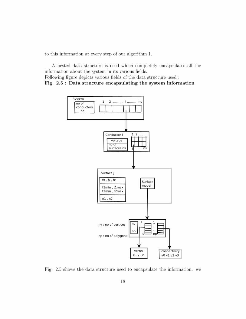
A nested data structure is used which completely encapsulates all theinformation about the system in its various fields.Following figure depicts various fields of the data structure used :Fig. 2.5 : Data structure encapsulating the system information
no of conductors
nc
1 2 ........... i ......... nc
Conductor i
voltageno of surfaces ns
1 2......
j......... ns
Surface j
fx , fy , fz
t1min , t1maxt2min , t2max
n1 , n2
Surface model
nv
np
1..nv
1..np
x , y , zvertex connectivity
v0 v1 v2 v3
nv : no of vertices
np : no of polygons
System
Fig. 2.5 shows the data structure used to encapsulate the information. we
18

can see that some of its fields are directly initialized by user input . theremaining fields are initialized by algorithms 2 , 3 and 4.
Once the geometry is generated, discretized and saved in the data struc-ture, finding charges is fairly straight forward.All that is to be done is to compute the centroids of the panels and form theBEM coefficient matrix according as (2.17) and then solve the linear system(2.16) to find the unknown charges.As the system is symmetric positive definite, we can use cholesky decompo-sition to solve the linear set of equations given by (2.16).
The results of BEM charge solver is discussed in Results and valida-tion section.
Thus we now have a mechanism to implement step 2 of our algorithm 1.the next main task concerns implementation of step 3. that is the topic ofnext section.
19
3 Mechanical Analysis by using 1D beam model
In this section, I shall give a brief account of details involved in implementingstep 3 of algorithm 1.i.e. How to find the deflection given the charge distribution?By assuming that shear is negligible, we only concentrate on lateral bendingof rectangular strip.To find the deflection, we need to to determine the forces causing them. sothat will be our first step.
After step 2 of algorithm 1, we have determined the charge distribution onthe surface of both conductors.i.e. both the conductors are discretized into rectangular panels and we havepoint charges residing on the centroids of each panel.As the lower plate is fixed, we are only interested in determining the forcesacting the upper deformable plate.As we know the charges, we can determine electrostatic force acting at thecentroid of any panel on the upper plate as following.
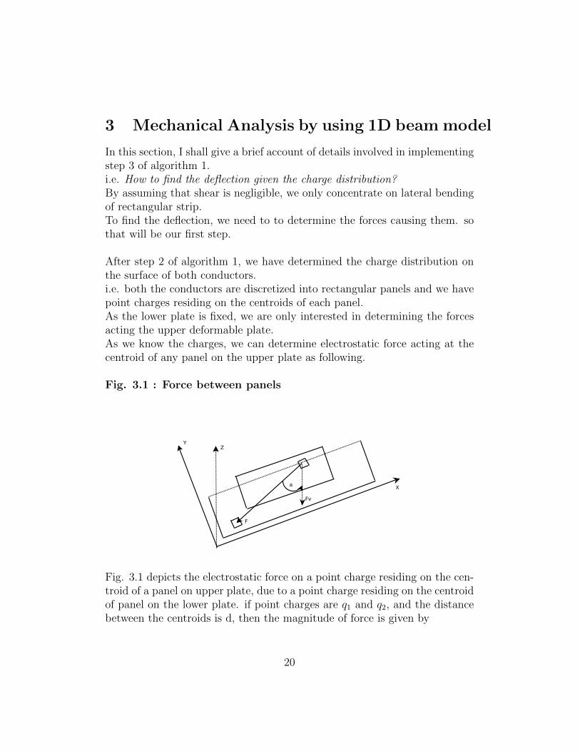
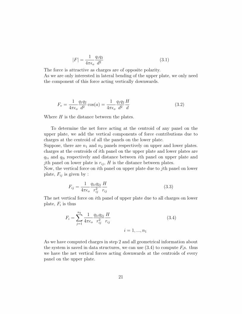
Fig. 3.1 : Force between panels
X
YZ
F
Fv
a
Fig. 3.1 depicts the electrostatic force on a point charge residing on the cen-troid of a panel on upper plate, due to a point charge residing on the centroidof panel on the lower plate. if point charges are q1 and q2, and the distancebetween the centroids is d, then the magnitude of force is given by
20
|F | = 1
4πεo
q1q2d2
(3.1)
The force is attractive as charges are of opposite polarity.As we are only interested in lateral bending of the upper plate, we only needthe component of this force acting vertically downwards.
Fv =1
4πεo
q1q2d2
cos(a) =1
4πεo
q1q2d2
H
d(3.2)
Where H is the distance between the plates.
To determine the net force acting at the centroid of any panel on theupper plate, we add the vertical components of force contributions due tocharges at the centroid of all the panels on the lower plate.Suppose, there are n1 and n2 panels respectively on upper and lower plates.charges at the centroids of ith panel on the upper plate and lower plates areq1i and q2i respectively and distance between ith panel on upper plate andjth panel on lower plate is rij, H is the distance between plates.Now, the vertical force on ith panel on upper plate due to jth panel on lowerplate, Fij is given by :
Fij =1
4πεo
q1iq2jr2ij
H
rij(3.3)
The net vertical force on ith panel of upper plate due to all charges on lowerplate, Fi is thus
Fi =
n2∑j=1
1
4πεo
q1iq2jr2ij
H
rij(3.4)
i = 1, ..., n1
As we have computed charges in step 2 and all geometrical information aboutthe system is saved in data structures, we can use (3.4) to compute Fis. thuswe have the net vertical forces acting downwards at the centroids of everypanel on the upper plate.
21
Next task is to compute the deflection. We have used a 1D beam modelfor the upper plate to compute the deflection.We have Euler-Bernoulli equation governing the mechanical deformation ofa beam :
EI∂4w
∂x4+ ρ
∂2w
∂t2= F (x) (3.5)
Beam is modelled as a 1 dimensional object.w(x) is the deflection at some position x.ρ : mass per unit length of the beam.E is the young’s modulus of the material of the beam.I second moment of area with respect to centroidal axis, perpendicular to
applied loading (=wt3b12
)w : width of the beam, tb : thickness of the beam.F is the distributed load or force per unit length.
For static analysis there is no time dependence and the time derivative maybe eliminated giving :
EId4w
dx4= F (x) (3.6)
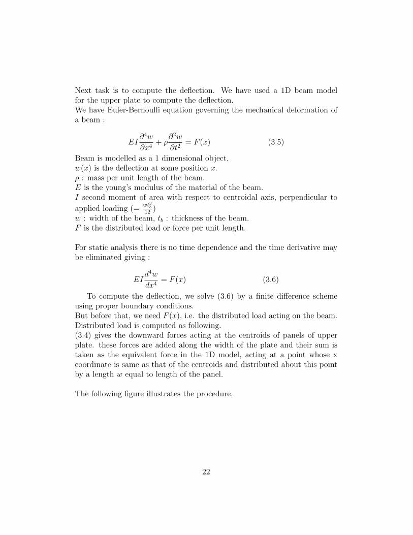
To compute the deflection, we solve (3.6) by a finite difference schemeusing proper boundary conditions.But before that, we need F (x), i.e. the distributed load acting on the beam.Distributed load is computed as following.(3.4) gives the downward forces acting at the centroids of panels of upperplate. these forces are added along the width of the plate and their sum istaken as the equivalent force in the 1D model, acting at a point whose xcoordinate is same as that of the centroids and distributed about this pointby a length w equal to length of the panel.
The following figure illustrates the procedure.
22
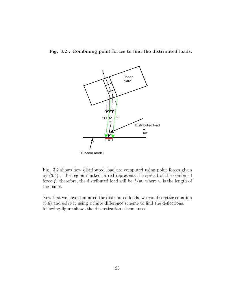
Fig. 3.2 : Combining point forces to find the distributed loads.
f1+ f2 + f3 = f
w
Distributed load = f/w
Upperplate
1D beam model
Fig. 3.2 shows how distributed load are computed using point forces givenby (3.4) . the region marked in red represents the spread of the combinedforce f . therefore, the distributed load will be f/w. where w is the length ofthe panel.
Now that we have computed the distributed loads, we can discretize equation(3.6) and solve it using a finite difference scheme to find the deflections.following figure shows the discretization scheme used.
23
Fig. 3.3 : Discretization of 1D domain of solution.
1 2 3 ............................ n
L
h
-1 0 n+1 n+2
Upper plate(panelized)
1D domain of solution
Fig. 3.3 shows the 1D discretization of the domain of solution using thediscretization of the upper plate.the length of the domain is discretized to nnodes where we wish to find the deflection.L is the length of the upper plate.h is the distance between centroids of adjacent panels.For convenience, we write the governing equation again along with boundaryconditions.
EId4w
dx4= F (x)
w(0) = 0.0
dw
dx
∣∣∣∣x=0
= 0.0
d2w
dx2
∣∣∣∣x=L
= 0.0
d3w
dx3
∣∣∣∣x=L
= 0.0
(3.7)
24
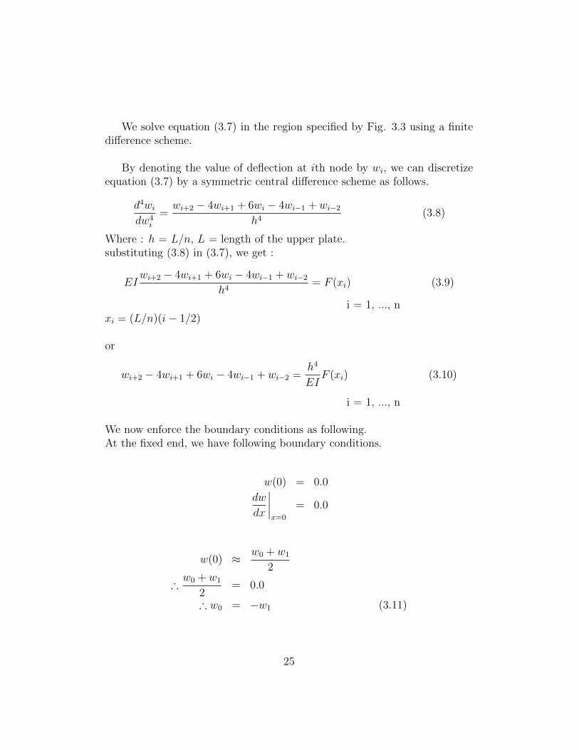
We solve equation (3.7) in the region specified by Fig. 3.3 using a finitedifference scheme.
By denoting the value of deflection at ith node by wi, we can discretizeequation (3.7) by a symmetric central difference scheme as follows.
d4widw4
i
=wi+2 − 4wi+1 + 6wi − 4wi−1 + wi−2
h4(3.8)
Where : h = L/n, L = length of the upper plate.substituting (3.8) in (3.7), we get :
EIwi+2 − 4wi+1 + 6wi − 4wi−1 + wi−2
h4= F (xi) (3.9)
i = 1, ..., nxi = (L/n)(i− 1/2)
or
wi+2 − 4wi+1 + 6wi − 4wi−1 + wi−2 =h4
EIF (xi) (3.10)
i = 1, ..., n
We now enforce the boundary conditions as following.At the fixed end, we have following boundary conditions.
w(0) = 0.0
dw
dx
∣∣∣∣x=0
= 0.0
w(0) ≈ w0 + w1
2
∴w0 + w1
2= 0.0
∴ w0 = −w1 (3.11)
25
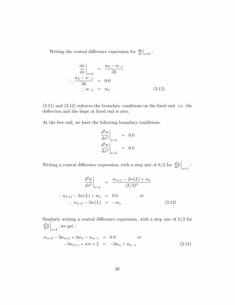
Writing the central difference expression for dwdx
∣∣x=0
:
dw
dx
∣∣∣∣x=0
=w2 − w−1
3h
∴w2 − w−1
3h= 0.0
∴ w−1 = w2 (3.12)
(3.11) and (3.12) enforces the boundary conditions on the fixed end. i.e. thedeflection and the slope at fixed end is zero.
At the free end, we have the following boundary conditions:
d2w
dx2
∣∣∣∣x=L
= 0.0
d3w
dx3
∣∣∣∣x=L
= 0.0
Writing a central difference expression, with a step size of h/2 for d2wdx2
∣∣∣x=L
:
d2w
dx2
∣∣∣∣x=L
=wn+1 − 2w(L) + wn
(h/2)2
∴ wn+1 − 2w(L) + wn = 0.0 or
∴ wn+1 − 2w(L) = −wn (3.13)
Similarly writing a central difference expression, with a step size of h/2 ford3wdx3
∣∣∣x=L
, we get :
wn+2 − 3wn+1 + 3wn − wn−1 = 0.0 or
−3wn+1 + wn+ 2 = −3wn + wn−1 (3.14)
26
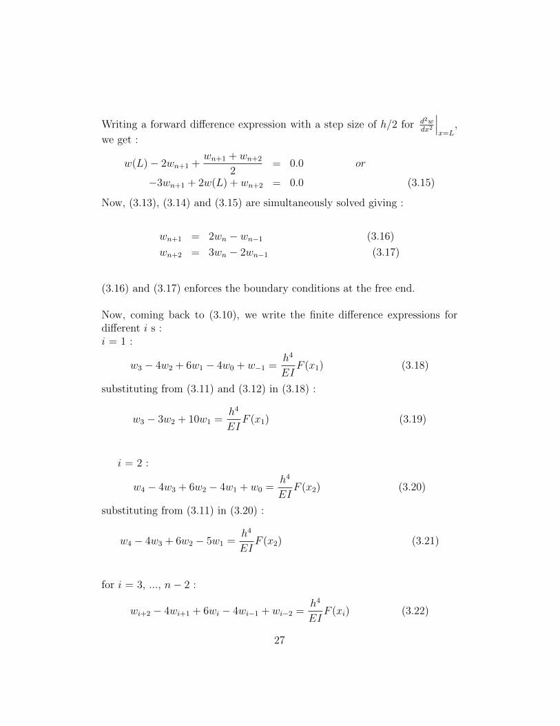
Writing a forward difference expression with a step size of h/2 for d2wdx2
∣∣∣x=L
,
we get :
w(L)− 2wn+1 +wn+1 + wn+2
2= 0.0 or
−3wn+1 + 2w(L) + wn+2 = 0.0 (3.15)
Now, (3.13), (3.14) and (3.15) are simultaneously solved giving :
wn+1 = 2wn − wn−1 (3.16)
wn+2 = 3wn − 2wn−1 (3.17)
(3.16) and (3.17) enforces the boundary conditions at the free end.
Now, coming back to (3.10), we write the finite difference expressions fordifferent i s :i = 1 :
w3 − 4w2 + 6w1 − 4w0 + w−1 =h4
EIF (x1) (3.18)
substituting from (3.11) and (3.12) in (3.18) :
w3 − 3w2 + 10w1 =h4
EIF (x1) (3.19)
i = 2 :
w4 − 4w3 + 6w2 − 4w1 + w0 =h4
EIF (x2) (3.20)
substituting from (3.11) in (3.20) :
w4 − 4w3 + 6w2 − 5w1 =h4
EIF (x2) (3.21)
for i = 3, ..., n− 2 :
wi+2 − 4wi+1 + 6wi − 4wi−1 + wi−2 =h4
EIF (xi) (3.22)
27
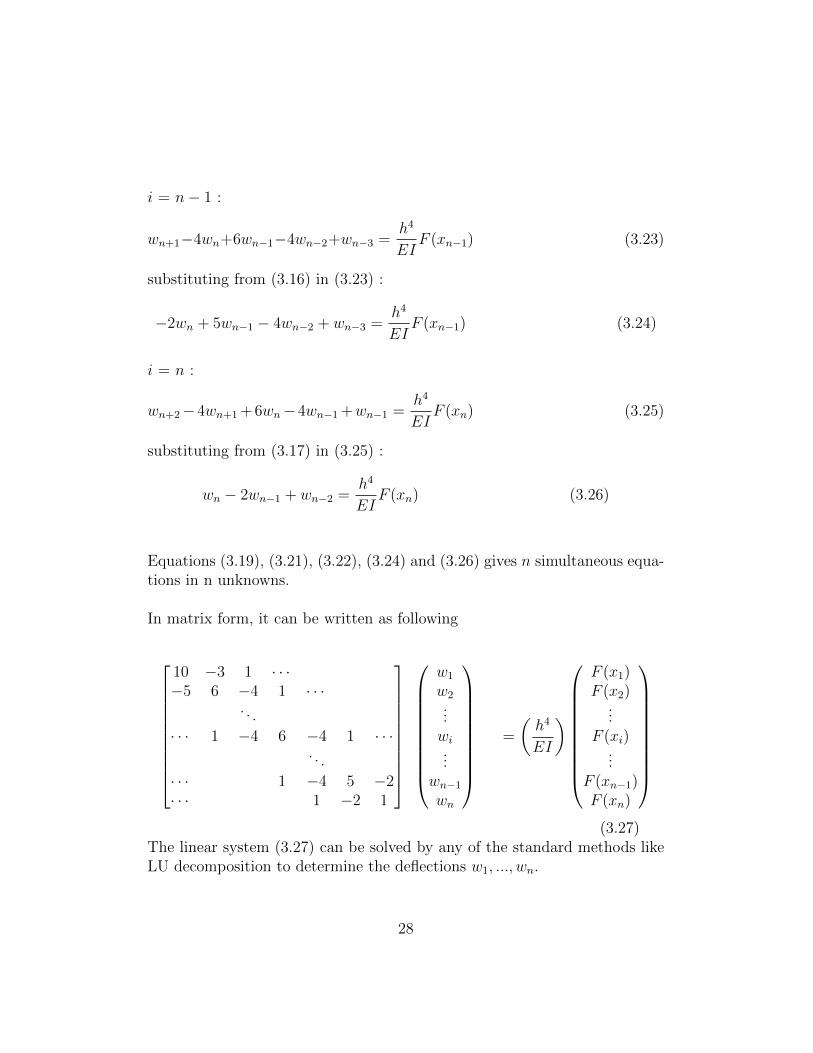
i = n− 1 :
wn+1−4wn+6wn−1−4wn−2+wn−3 =h4
EIF (xn−1) (3.23)
substituting from (3.16) in (3.23) :
−2wn + 5wn−1 − 4wn−2 + wn−3 =h4
EIF (xn−1) (3.24)
i = n :
wn+2−4wn+1 + 6wn−4wn−1 +wn−1 =h4
EIF (xn) (3.25)
substituting from (3.17) in (3.25) :
wn − 2wn−1 + wn−2 =h4
EIF (xn) (3.26)
Equations (3.19), (3.21), (3.22), (3.24) and (3.26) gives n simultaneous equa-tions in n unknowns.
In matrix form, it can be written as following
10 −3 1 · · ·−5 6 −4 1 · · ·
. . .
· · · 1 −4 6 −4 1 · · ·. . .
· · · 1 −4 5 −2· · · 1 −2 1
w1
w2...wi...
wn−1wn
=
(h4
EI
)
F (x1)F (x2)
...F (xi)
...F (xn−1)F (xn)
(3.27)
The linear system (3.27) can be solved by any of the standard methods likeLU decomposition to determine the deflections w1, ..., wn.
28
We now have the method to determine the deflections given the charges.the step 4 of the Algorithm 1 is to update the geometry. this is fairly simple.we just update the centroids all panels whose x coordinates are same by thevalue corresponding to deflection for the same x value obtained by solving(3.27).Note that, mechanical analysis is at every step is done with respect to initialconfiguration.i.e. (geometry at ith step) = (initial configuration) + (deflection at ith step)electrical analysis is done with respect to deformed geometry to find thecharges and hence the forces.This concludes our discussion of mechanical analysis.
Having explained the methods involved in implementing algorithm 1, I shallgive a brief account of results obtained by using these methods in the nextsection.
29
4 Results and Validation
In this section, I shall discuss the results obtained by using the methods ex-plained in previous sections.Results of electrical and mechanical analysis explained in sections 2 and 3are individually discussed and finally the results of applying the methods forthe coupled problem is discussed.
Now, I shall give a brief account of results obtained by using BEM methodto solve for induced charge distribution on various conductor configurations.
case 1 Consider a conductor sphere held at some potential V .It can be shown analytically that the total charge induced on the surface ofthe sphere, Q is :
Q = 4πεoV r (4.1)
r is radius of the sphere.Q is uniformly distributed over the surface.
Suppose, we take a sphere of radius 1mm and hold it at a potential of10volts.From (4.1), total charge induced on it is 0.001111nC and surface charge den-sity is 88.419nC/m2.
We now solve the above problem by using the BEM method described insection 2 and add all the charges computed at centroids of the panels.The sum of all charges at the centroids of the panels is 0.001112nC. thecharge contained in any part of the surface is measured and found to be pro-portional to the area of that part. this shows that the charges are uniformlydistributed and validates our method with reference to analytical result of(4.1).
case 2 Consider a rectangular strip held at a voltage V . although, we donot have a closed form expression for the charge distribution, we know cer-tain properties it should have. the charge distribution will be more near theedges and maximum at the corners. this is to be expected as like chargesrepel each other and get separated from each other and concentrate near the
30
edges and corners.
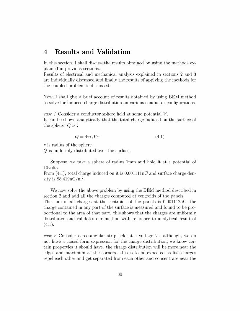
We solve for charges on a 1× 0.5 mm rectangular strip held at 10V.The following figure depicts the surface charge distribution.
Fig. 4.1 : Charge distribution on a 1 × 0.5mm rectangular stripheld at 10V
05
1015
20
0
10
20
30
400
0.5
1
1.5
2
2.5
x 10−6
panel index along width
charge distribution on a rectangular strip
panel index along length
char
ge in
nC
It is clearly seen from figure 4.1 that charge distribution is more concentratednear the edges and is maximum in the corners.
case 3 Two rectangular plates parallel to each other.
31
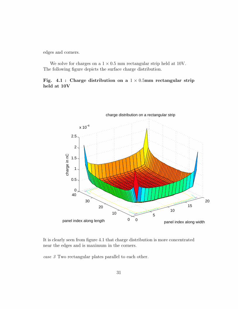
Consider 2 rectangular parallel plates each of dimension 1 × 0.5 mm . dis-tance between the plate is 0.2mm. upper plate is held at 10V and lower plateat 0V.Solving for charges on the 2 plates using BEM method, we get a charge dis-tribution as depicted by the following figure.
Fig. 4.2 : Charge distribution on parallel plates each of dimen-sion 1× 0.5 mm , upper plate held at 10V and lower plate at 0V
05
1015
20
0
10
20
30
40−2
−1
0
1
2
3
x 10−6
panel index along width
charge distribution on parallel plates
panel index along length
char
ge in
nC
We see from Fig. 4.2 that presence of another plate increases the charges onupper plate. although lower plate is held at 0V, negative charges are inducedon it as expected.
32
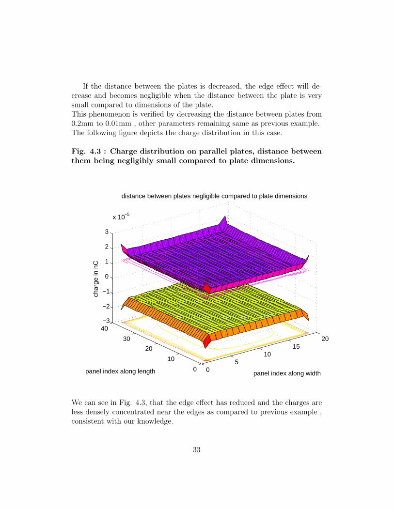
If the distance between the plates is decreased, the edge effect will de-crease and becomes negligible when the distance between the plate is verysmall compared to dimensions of the plate.This phenomenon is verified by decreasing the distance between plates from0.2mm to 0.01mm , other parameters remaining same as previous example.The following figure depicts the charge distribution in this case.
Fig. 4.3 : Charge distribution on parallel plates, distance betweenthem being negligibly small compared to plate dimensions.
05
1015
20
0
10
20
30
40−3
−2
−1
0
1
2
3
x 10−5
panel index along width
distance between plates negligible compared to plate dimensions
panel index along length
char
ge in
nC
We can see in Fig. 4.3, that the edge effect has reduced and the charges areless densely concentrated near the edges as compared to previous example ,consistent with our knowledge.
33
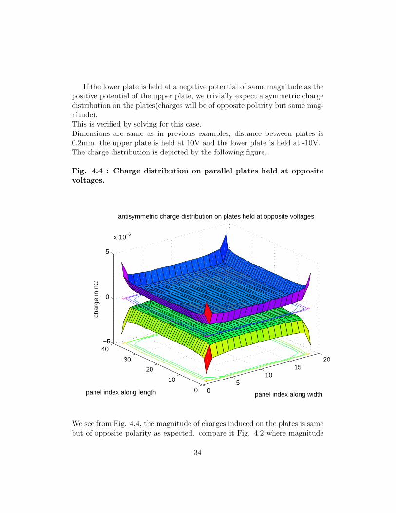
If the lower plate is held at a negative potential of same magnitude as thepositive potential of the upper plate, we trivially expect a symmetric chargedistribution on the plates(charges will be of opposite polarity but same mag-nitude).This is verified by solving for this case.Dimensions are same as in previous examples, distance between plates is0.2mm. the upper plate is held at 10V and the lower plate is held at -10V.The charge distribution is depicted by the following figure.
Fig. 4.4 : Charge distribution on parallel plates held at oppositevoltages.
05
1015
20
0
10
20
30
40−5
0
5
x 10−6
panel index along width
antisymmetric charge distribution on plates held at opposite voltages
panel index along length
char
ge in
nC
We see from Fig. 4.4, the magnitude of charges induced on the plates is samebut of opposite polarity as expected. compare it Fig. 4.2 where magnitude
34
of charges is higher on the upper plate.
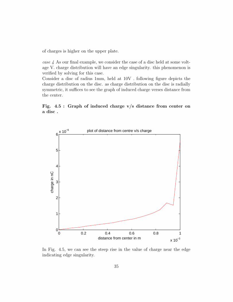
case 4 As our final example, we consider the case of a disc held at some volt-age V. charge distribution will have an edge singularity. this phenomenon isverified by solving for this case.Consider a disc of radius 1mm, held at 10V . following figure depicts thecharge distribution on the disc. as charge distribution on the disc is radiallysymmetric, it suffices to see the graph of induced charge verses distance fromthe center.
Fig. 4.5 : Graph of induced charge v/s distance from center ona disc .
0 0.2 0.4 0.6 0.8 1
x 10−3
0
1
2
3
4
5
6x 10⁻⁶ plot of distance from centre v/s charge
distance from center in m
char
ge in
nC
In Fig. 4.5, we can see the steep rise in the value of charge near the edgeindicating edge singularity.
35
The above examples validates our BEM implementation for solving for stati-cally induced charges hence allowing us to use it for effective implementationof step 2 of algorithm 1.
Now, I shall give a brief account of results of mechanical analysis. as ex-plained in section 3, we have used a 1D beam model and to find the deflec-tion, we solve the following equation by a finite difference scheme :
EId4w
dx4= F (x)
w(0) = 0.0
dw
dx
∣∣∣∣x=0
= 0.0
d2w
dx2
∣∣∣∣x=L
= 0.0
d3w
dx3
∣∣∣∣x=L
= 0.0
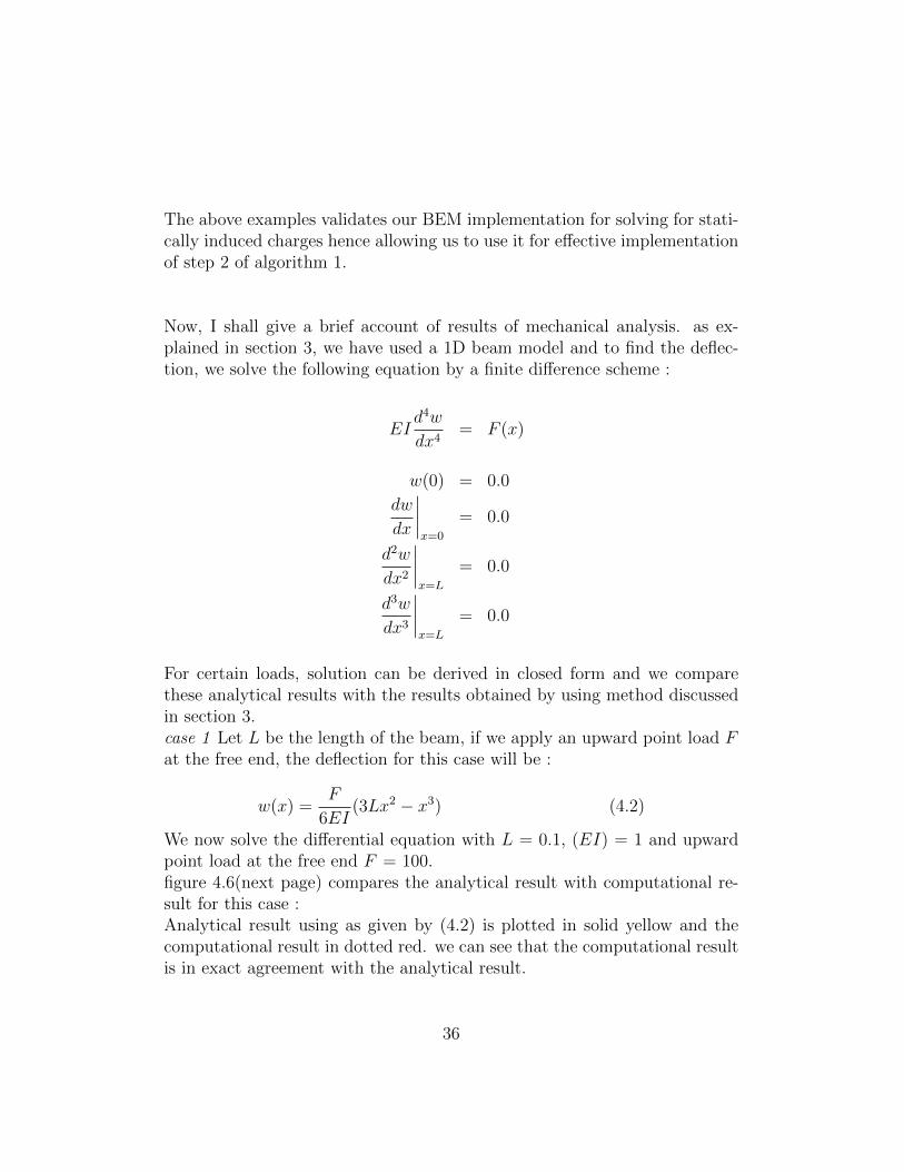
For certain loads, solution can be derived in closed form and we comparethese analytical results with the results obtained by using method discussedin section 3.case 1 Let L be the length of the beam, if we apply an upward point load Fat the free end, the deflection for this case will be :
w(x) =F
6EI(3Lx2 − x3) (4.2)
We now solve the differential equation with L = 0.1, (EI) = 1 and upwardpoint load at the free end F = 100.figure 4.6(next page) compares the analytical result with computational re-sult for this case :Analytical result using as given by (4.2) is plotted in solid yellow and thecomputational result in dotted red. we can see that the computational resultis in exact agreement with the analytical result.
36
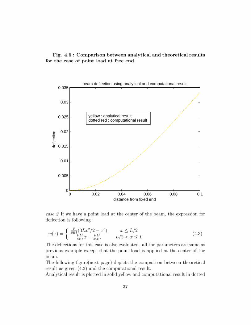
Fig. 4.6 : Comparison between analytical and theoretical resultsfor the case of point load at free end.
0 0.02 0.04 0.06 0.08 0.10
0.005
0.01
0.015
0.02
0.025
0.03
0.035
distance from fixed end
defle
ctio
n
beam deflection using analytical and computational result
yellow : analytical resultdotted red : computational result
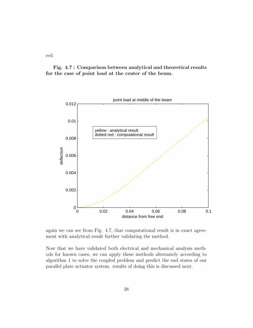
case 2 If we have a point load at the center of the beam, the expression fordeflection is following :
w(x) =
{F
6EI(3Lx2/2− x3) x ≤ L/2FL2
8EIx− FL3
48EIL/2 < x ≤ L
(4.3)
The deflections for this case is also evaluated. all the parameters are same asprevious example except that the point load is applied at the center of thebeam.The following figure(next page) depicts the comparison between theoreticalresult as given (4.3) and the computational result.Analytical result is plotted in solid yellow and computational result in dotted
37
red.
Fig. 4.7 : Comparison between analytical and theoretical resultsfor the case of point load at the center of the beam.
0 0.02 0.04 0.06 0.08 0.10
0.002
0.004
0.006
0.008
0.01
0.012
distance from free end
defle
ctio
n
point load at middle of the beam
yellow : analytical resultdotted red : computational result
again we can see from Fig. 4.7, that computational result is in exact agree-ment with analytical result further validating the method.
Now that we have validated both electrical and mechanical analysis meth-ods for known cases, we can apply these methods alternately according toalgorithm 1 to solve the coupled problem and predict the end states of ourparallel plate actuator system. results of doing this is discussed next.
38
As explained in the introduction section, there are 2 end states for ourparallel plate actuator system. for a given configuration and voltage , thesystem ends up in one of these end states . i.e., it will either go to its equi-librium deformation state or it will touch the lower conductor resulting in aPull-in.
Now, I shall present the results for 2 different configurations.
Configuration 1 :Dimensions of upper plate : 400µm × 10µmDimensions of lower plate : 8mm × 0.2mm . centroids of the plates arevertically aligned.Distance between the plates : 5µmThickness of the upper plate : 0.3µmYoung’s modulus of material(silicon) of the conductor :E = 160× 109Pa
The following figures(next page) depict the end states for this configura-tion for various voltages.
39
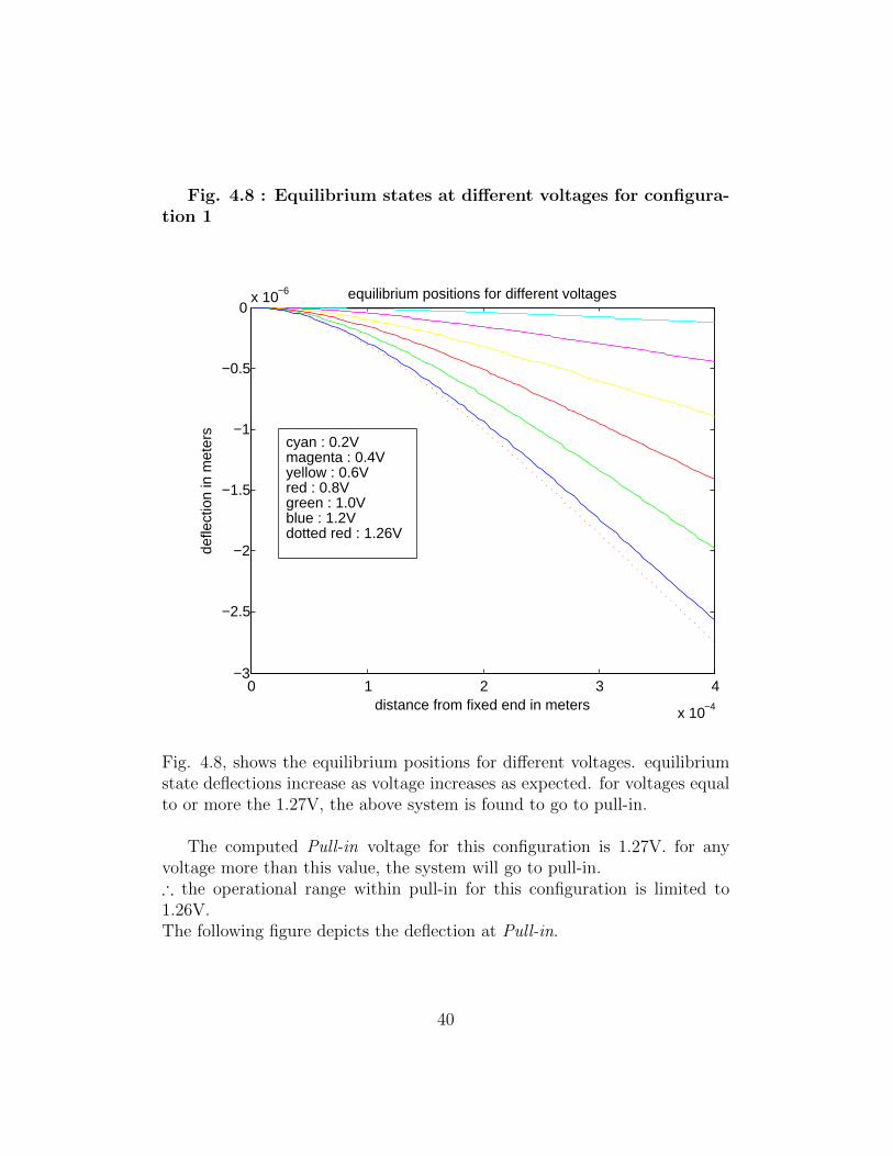
Fig. 4.8 : Equilibrium states at different voltages for configura-tion 1
0 1 2 3 4
x 10−4
−3
−2.5
−2
−1.5
−1
−0.5
0x 10−6
distance from fixed end in meters
defle
ctio
n in
met
ers
equilibrium positions for different voltages
cyan : 0.2Vmagenta : 0.4Vyellow : 0.6Vred : 0.8Vgreen : 1.0Vblue : 1.2Vdotted red : 1.26V
Fig. 4.8, shows the equilibrium positions for different voltages. equilibriumstate deflections increase as voltage increases as expected. for voltages equalto or more the 1.27V, the above system is found to go to pull-in.
The computed Pull-in voltage for this configuration is 1.27V. for anyvoltage more than this value, the system will go to pull-in.∴ the operational range within pull-in for this configuration is limited to1.26V.The following figure depicts the deflection at Pull-in.
40
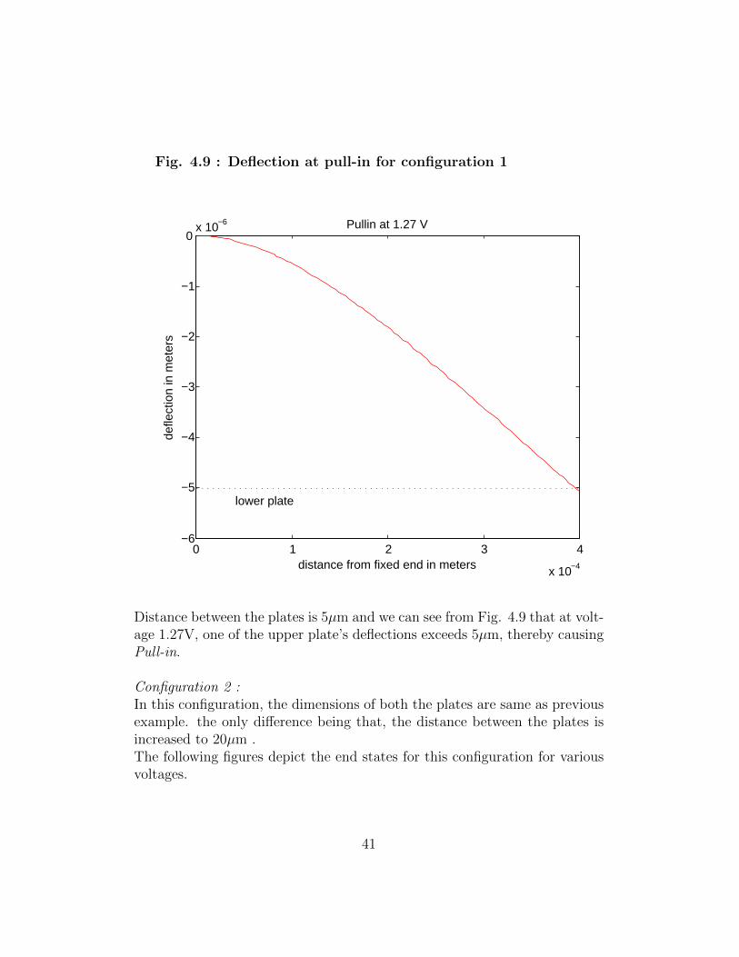
Fig. 4.9 : Deflection at pull-in for configuration 1
0 1 2 3 4
x 10−4
−6
−5
−4
−3
−2
−1
0x 10−6
distance from fixed end in meters
defle
ctio
n in
met
ers
Pullin at 1.27 V
lower plate
Distance between the plates is 5µm and we can see from Fig. 4.9 that at volt-age 1.27V, one of the upper plate’s deflections exceeds 5µm, thereby causingPull-in.
Configuration 2 :In this configuration, the dimensions of both the plates are same as previousexample. the only difference being that, the distance between the plates isincreased to 20µm .The following figures depict the end states for this configuration for variousvoltages.
41
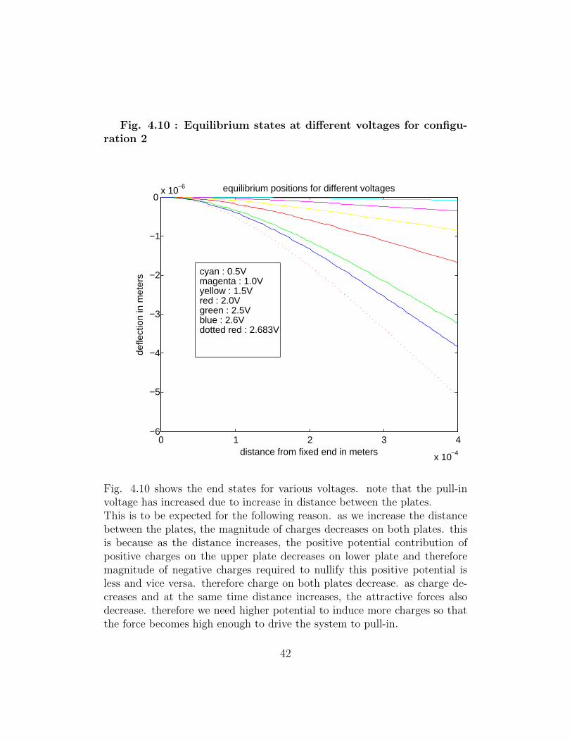
Fig. 4.10 : Equilibrium states at different voltages for configu-ration 2
0 1 2 3 4
x 10−4
−6
−5
−4
−3
−2
−1
0x 10−6
distance from fixed end in meters
defle
ctio
n in
met
ers
equilibrium positions for different voltages
cyan : 0.5Vmagenta : 1.0Vyellow : 1.5Vred : 2.0Vgreen : 2.5Vblue : 2.6Vdotted red : 2.683V
Fig. 4.10 shows the end states for various voltages. note that the pull-involtage has increased due to increase in distance between the plates.This is to be expected for the following reason. as we increase the distancebetween the plates, the magnitude of charges decreases on both plates. thisis because as the distance increases, the positive potential contribution ofpositive charges on the upper plate decreases on lower plate and thereforemagnitude of negative charges required to nullify this positive potential isless and vice versa. therefore charge on both plates decrease. as charge de-creases and at the same time distance increases, the attractive forces alsodecrease. therefore we need higher potential to induce more charges so thatthe force becomes high enough to drive the system to pull-in.
42
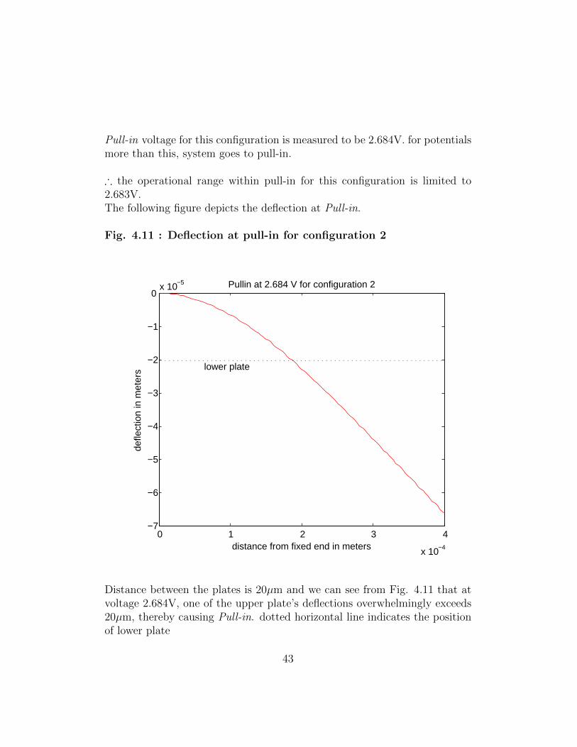
Pull-in voltage for this configuration is measured to be 2.684V. for potentialsmore than this, system goes to pull-in.
∴ the operational range within pull-in for this configuration is limited to2.683V.The following figure depicts the deflection at Pull-in.
Fig. 4.11 : Deflection at pull-in for configuration 2
0 1 2 3 4
x 10−4
−7
−6
−5
−4
−3
−2
−1
0x 10−5
distance from fixed end in meters
defle
ctio
n in
met
ers
Pullin at 2.684 V for configuration 2
lower plate
Distance between the plates is 20µm and we can see from Fig. 4.11 that atvoltage 2.684V, one of the upper plate’s deflections overwhelmingly exceeds20µm, thereby causing Pull-in. dotted horizontal line indicates the positionof lower plate
43

Having presented in this section, the results of applying the methods de-scribed in previous sections, I thus conclude this section on results and vali-dation.
44
5 Conclusion
As claimed in the introduction of the thesis, a computational scheme has beendesigned for analysis of parallel plate systems. the BEM solver described insection 2 is implemented to solve a more generic problem, i.e. to solve forcharge distribution of any arbitrary layout of conductors with their geome-tries specified. the panels should be small enough so that our approximationis validated. BEM matrices are full matrices and storage cost is more. stor-age cost may be reduced by considering that BEM matrices are symmetric.By this scheme, we are able to predict the end state(up to pull-in) of anyparallel plate system with relatively low computational cost. 3D methodswhich use FEM are computationally more costly. the 1D beam model forupper plate is a good approximation when length is large compared to thewidth of the plate which is generally the case and it greatly simplifies theproblem and gives reasonably accurate results.
45
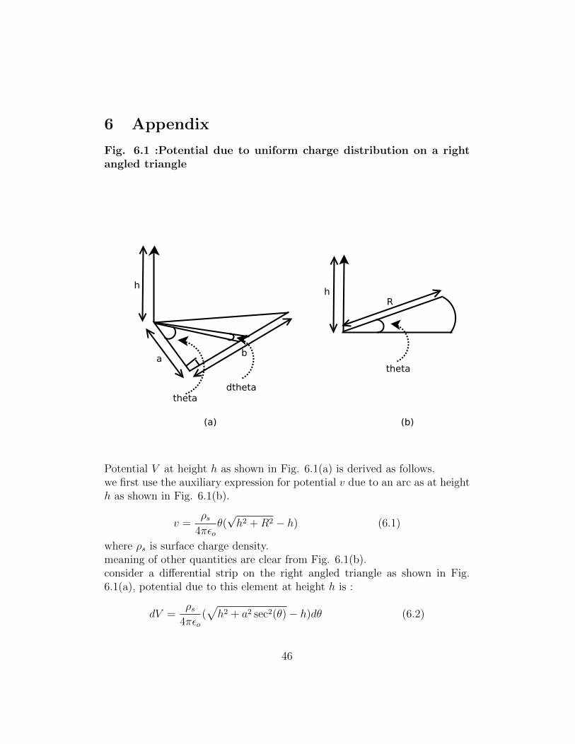
6 Appendix
Fig. 6.1 :Potential due to uniform charge distribution on a rightangled triangle
theta
a
h
dtheta
b
hR
theta
(a) (b)
Potential V at height h as shown in Fig. 6.1(a) is derived as follows.we first use the auxiliary expression for potential v due to an arc as at heighth as shown in Fig. 6.1(b).
v =ρs
4πεoθ(√h2 +R2 − h) (6.1)
where ρs is surface charge density.meaning of other quantities are clear from Fig. 6.1(b).consider a differential strip on the right angled triangle as shown in Fig.6.1(a), potential due to this element at height h is :
dV =ρs
4πεo(√h2 + a2 sec2(θ)− h)dθ (6.2)
46
potential due to entire triangle is obtained by integrating (6.2), through-out the area of triangle.
V =ρs
4πεo
∫ ψ
0
(√h2 + a2 sec2(θ)− h)dθ (6.3)
where ψ is the angle at the vertex below the point where we desire to findthe potential.(6.3) reduces to :
V =ρs
4πεo
[∫ ψ
0
√h2 + a2 sec2(θ)dθ − hψ
](6.4)
integral in (6.4) is evaluated as follows :∫ ψ
0
√h2 + a2 sec2(θ)dθ = a
∫ ψ
0
√(h/a)2 + sec2(θ)dθ (6.5)
letting (h/a) = m ;∫ ψ
0
√h2 + a2 sec2(θ)dθ = a
∫ ψ
0
√m2 + sec2(θ)dθ (6.6)
integral in (6.6) is evaluated as follows :
∫ ψ
0
√m2 + sec2(θ)dθ =
∫ ψ
0
m2 + sec2(θ)√m2 + sec2(θ)
dθ
= m2
∫ ψ
0
dθ√m2 + sec2(θ)
+
∫ ψ
0
sec2(θ)√m2 + sec2(θ)
dθ
= m2I1 + I2 (6.7)
integrals I1 and I2 are evaluated as follows :
I1 =
∫ ψ
0
dθ√m2 + sec2(θ)
=
∫ ψ
0
cos(θ)√1 +m2 cos2(θ)
dθ
47
letting sin(θ) = t, cos(θ)dθ = dt substituting in previous equation :
I1 =
∫ sin(ψ)
0
dt√1 +m2(1− t2)
=
∫ sin(ψ)
0
dt√(1 +m2)− (mt2)
=1
m
∫ sin(ψ)
0
dt√1+m2
m2 − t2
=1
marcsin
(mt√
1 +m2
)∣∣∣∣sin(ψ)0
=1
marcsin
(m sin(ψ)√
1 +m2
)=
a
harcsin
((h/a) sin(ψ)√
1 + (h/a)2
)
=a
harcsin
(h sin(ψ)√a2 + h2
)as sin(ψ) = b√
a2+b2:
I1 =a
harcsin
(hb√
(a2 + h2)(a2 + b2)
)(6.8)
I2 is evaluated as follows :
I2 =
∫ ψ
0
sec2(θ)√m2 + sec2(θ)
dθ
=
∫ ψ
0
sec2(θ)√m2 + 1 + tan2(θ)
dθ
letting tan(θ) = t, sec2(θ)dθ = dt :
48
∴ I2 =
∫ tan(ψ)
0
dt√m2 + 1 + t2
= ln(t+√m2 + 1 + t2)
∣∣∣tan(ψ)0
= ln
(tan(ψ) +
√m2 + 1 + tan2(ψ)√m2 + 1
)
substituting tan(ψ) = b/a and m = h/a :
I2 = ln
(b+√h2 + a2 + b2√a2 + h2
)(6.9)
substituting (6.9) and (6.8) in (6.7) and then back in (6.4), we get the fol-lowing expression for potential at height h from vertex of the right angledtriangle shown in Fig. 6.1 :
V =σs
4πεo
[h arcsin
(hb√
(a2 + b2)(a2 + h2)
)+ a ln
(b+√h2 + a2 + b2√h2 + a2
)
−h arctan
(b
a
)]
49
7 References
1. A Lagrangian approach to electrostatic analysis of deformable conduc-tors - Gang Li and N.R. Aluru, JOURNAL OF MICROELECTROME-CHANICAL SYSTEMS, VOL. 11, NO. 3, june 2002
2. Cantilever beam electrostatic MEMS actuators beyond Pull-in - Sub-rahmanyam Gorthi, Atanu Mohanty and Anindya Chatterjee, JOUR-NAL OF MICROMECHANICS AND MICROENGINEERING, July2006
3. Engineering Electromagnetics - William Hayt, 6th edition, PHI
4. Engineering Mechanics of Solids - Egor P Popov, 2nd edition, PHI
50