Embed Size (px)
Citation preview
Computer Organization 10CS46
Dept Of CSE, ACE Bangalore Page 1
Unit I Basic Structure of Computers Computer Architecture in general covers three aspects of computer design namely: Computer
Hardware, Instruction set Architecture and Computer Organization.
Computer hardware consists of electronic circuits, displays, magnetic and optical storage
mediaand communication facilities.
Instruction set Architecture is programmer visible machine interface such as instruction set,
registers, memory organization and exception handling. Two main approaches are mainly
CISC(Complex Instruction Set Computer) and RISC (Reduced Instruction Set Computer)
Computer Organization includes the high level aspects of a design, such as memory system, the bus
structure and the design of the internal CPU.
Computer Types
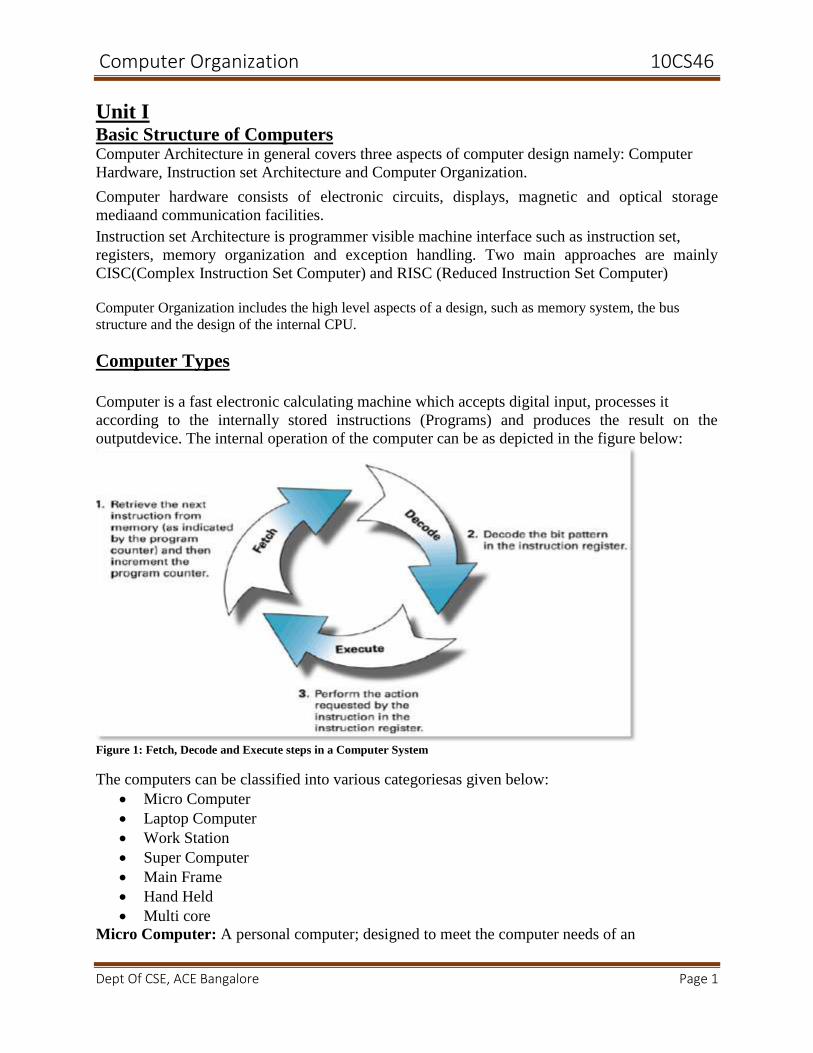
Computer is a fast electronic calculating machine which accepts digital input, processes it
according to the internally stored instructions (Programs) and produces the result on the
outputdevice. The internal operation of the computer can be as depicted in the figure below:
Figure 1: Fetch, Decode and Execute steps in a Computer System
The computers can be classified into various categoriesas given below:
Micro Computer
Laptop Computer
Work Station
Super Computer
Main Frame
Hand Held
Multi core
Micro Computer: A personal computer; designed to meet the computer needs of an
Computer Organization 10CS46
Dept Of CSE, ACE Bangalore Page 2
individual. Provides access to a wide variety of computing applications, such as word
processing,photo editing, e-mail, and internet.
Laptop Computer: A portable, compact computer that can run on power supply or a battery
unit. All components are integrated as one compact unit. It is generally more expensive than a
comparable desktop. It is also called a Notebook.
Work Station: Powerful desktop computer designed for specialized tasks. Generally used for
tasks that requires a lot of processing speed. Can also be an ordinary personal computer attached
to a LAN (local area network).
Super Computer: A computer that is considered to be fastest in the world. Used to execute
tasks that would take lot of time for other computers. For Ex: Modeling weather systems,
genome sequence, etc
Main Frame: Large expensive computer capable of simultaneously processing data for
hundreds or thousands of users. Used to store, manage, and process large amounts of data that
need to be reliable, secure, and centralized.
Hand Held: It is also called a PDA (Personal Digital Assistant). A computer that fits into a
pocket, runs on batteries, and is used while holding the unit in your hand. Typically used as an
appointment book, address book, calculator and notepad.
Multi Core: Have Multiple Cores – parallel computing platforms. Many Cores or computing
elements in a single chip. Typical Examples: Sony Play station, Core 2 Duo, i3, i7 etc.
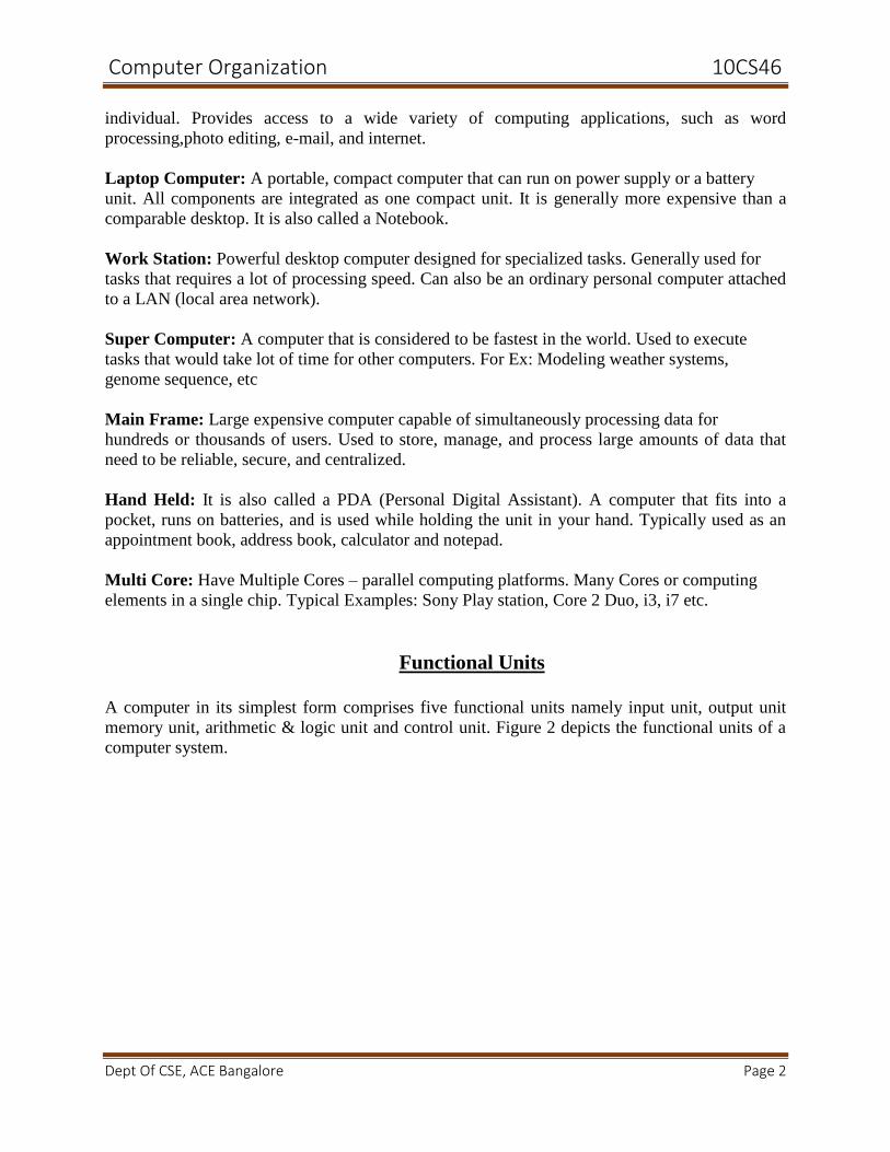
Functional Units
A computer in its simplest form comprises five functional units namely input unit, output unit
memory unit, arithmetic & logic unit and control unit. Figure 2 depicts the functional units of a
computer system.
Computer Organization 10CS46
Dept Of CSE, ACE Bangalore Page 3
Figure 2: Basic functional units of a computer
Let us discuss about each of them in brief:
1. Input Unit: Computer accepts encoded information through input unit. The standard input
device is a keyboard. Whenever a key is pressed, keyboard controller sends the code to
CPU/Memory.
Examples include Mouse, Joystick, Tracker ball, Light pen, Digitizer, Scanner etc.
2. Memory Unit: Memory unit stores the program instructions (Code), data and results of
computations etc. Memory unit is classified as:
• Primary /Main Memory
• Secondary /Auxiliary Memory
Primary memory is a semiconductor memory that provides access at high speed. Run time
program instructions and operands are stored in the main memory. Main memory is classified
again as ROM and RAM. ROM holds system programs and firmware routines such as BIOS,
POST, I/O Drivers that are essential to manage the hardware of a computer. RAM is termed as
Read/Write memory or user memory that holds run time program instruction and data. While
primary storage is essential, it is volatile in nature and expensive. Additional requirement of
memory could be supplied as auxiliary memory at cheaper cost. Secondary memories are non
volatile in nature.
3. Arithmetic and logic unit: ALU consist of necessary logic circuits like adder, comparator
etc., to perform operations of addition, multiplication, comparison of two numbers etc.
4. Output Unit: Computer after computation returns the computed results, error messages, etc.
via output unit. The standard output device is a video monitor, LCD/TFT monitor. Other output
devices are printers, plotters etc.
Computer Organization 10CS46
Dept Of CSE, ACE Bangalore Page 4
5. Control Unit: Control unit co-ordinates activities of all units by issuing control signals.
Control signals issued by control unit govern the data transfers and then appropriate operations
take place. Control unit interprets or decides the operation/action to be performed.
The operations of a computer can be summarized as follows:
1. A set of instructions called a program reside in the main memory of computer.
2. The CPU fetches those instructions sequentially one-by-one from the main memory, decodes
them and performs the specified operation on associated data operands in ALU.
3. Processed data and results will be displayed on an output unit.
4. All activities pertaining to processing and data movement inside the computer machine are
governed by control unit.
Basic Operational Concepts
An Instruction consists of two parts, an Operation code and operand/s as shown below:
Let us see a typical instruction
ADD LOCA, R0
This instruction is an addition operation. The following are the steps to execute the instruction:
Step 1: Fetch the instruction from main memory into the processor
Step 2: Fetch the operand at location LOCA from main memory into the processor
Step 3: Add the memory operand (i.e. fetched contents of LOCA) to the contents of register R0
Step 4: Store the result (sum) in R0.
The same instruction can be realized using two instructions as
Load LOCA, R1
Add R1, R0
The steps to execute the instructions can be enumerated as below:
Step 1: Fetch the instruction from main memory into the processor
Step 2: Fetch the operand at location LOCA from main memory into
the processor Register R1
Computer Organization 10CS46
Dept Of CSE, ACE Bangalore Page 5
Step 3: Add the content of Register R1 and the contents of register R0
Step 4: Store the result (sum) in R0.
OPCODE OPERAND/s
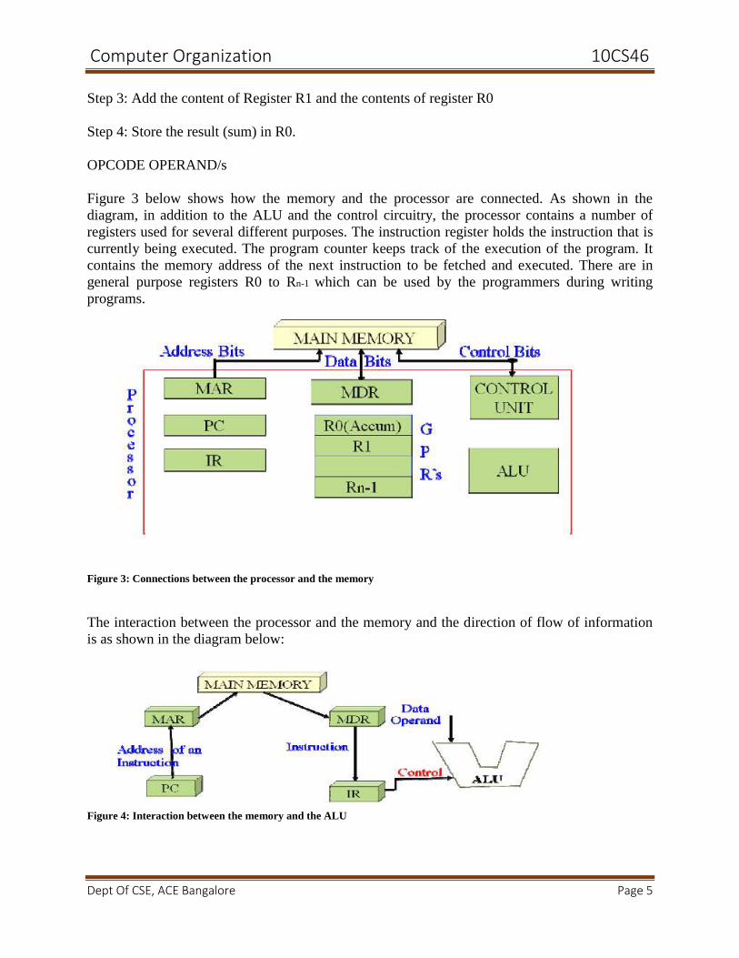
Figure 3 below shows how the memory and the processor are connected. As shown in the
diagram, in addition to the ALU and the control circuitry, the processor contains a number of
registers used for several different purposes. The instruction register holds the instruction that is
currently being executed. The program counter keeps track of the execution of the program. It
contains the memory address of the next instruction to be fetched and executed. There are in
general purpose registers R0 to Rn-1 which can be used by the programmers during writing
programs.
Figure 3: Connections between the processor and the memory
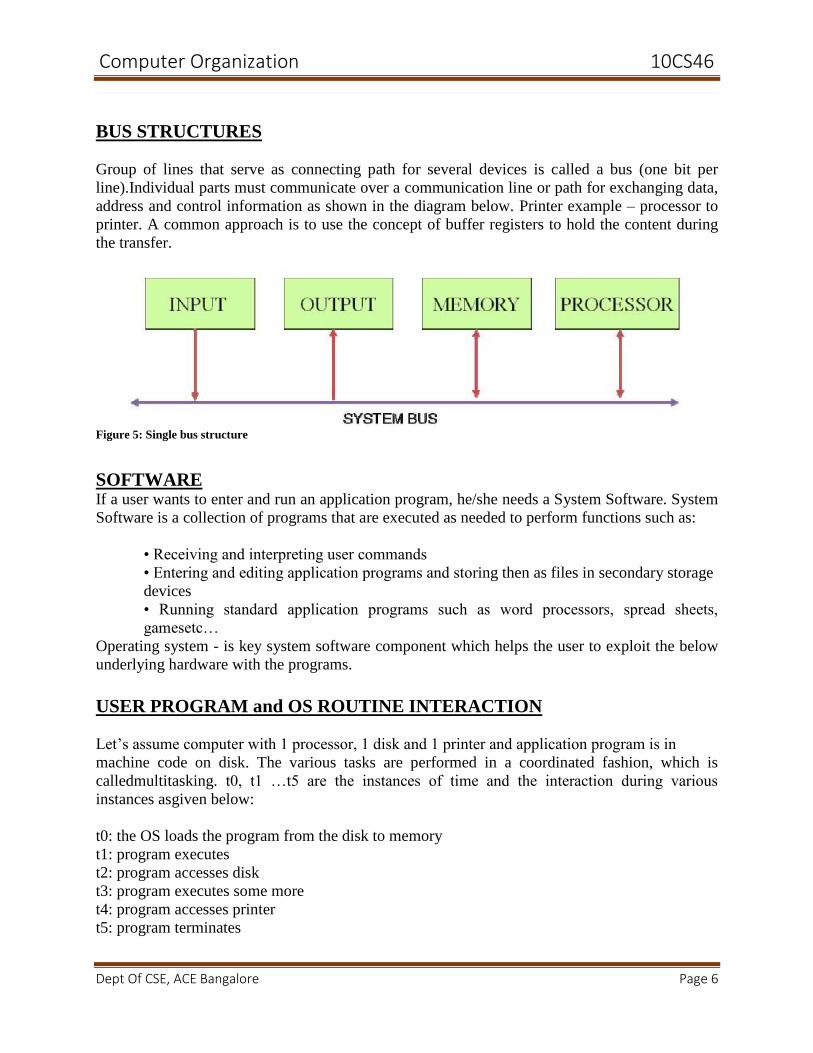
The interaction between the processor and the memory and the direction of flow of information
is as shown in the diagram below:
Figure 4: Interaction between the memory and the ALU
Computer Organization 10CS46
Dept Of CSE, ACE Bangalore Page 6
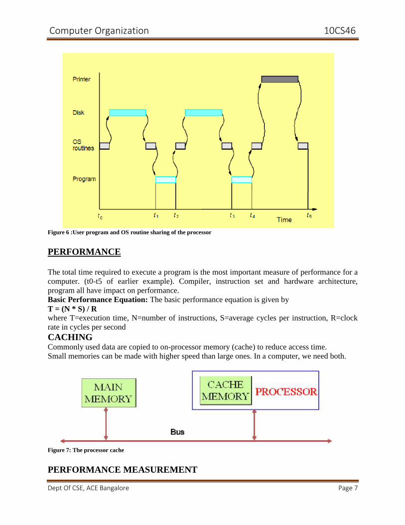
BUS STRUCTURES
Group of lines that serve as connecting path for several devices is called a bus (one bit per
line).Individual parts must communicate over a communication line or path for exchanging data,
address and control information as shown in the diagram below. Printer example – processor to
printer. A common approach is to use the concept of buffer registers to hold the content during
the transfer.
Figure 5: Single bus structure
SOFTWARE If a user wants to enter and run an application program, he/she needs a System Software. System
Software is a collection of programs that are executed as needed to perform functions such as:
• Receiving and interpreting user commands
• Entering and editing application programs and storing then as files in secondary storage
devices
• Running standard application programs such as word processors, spread sheets,
gamesetc…
Operating system - is key system software component which helps the user to exploit the below
underlying hardware with the programs.
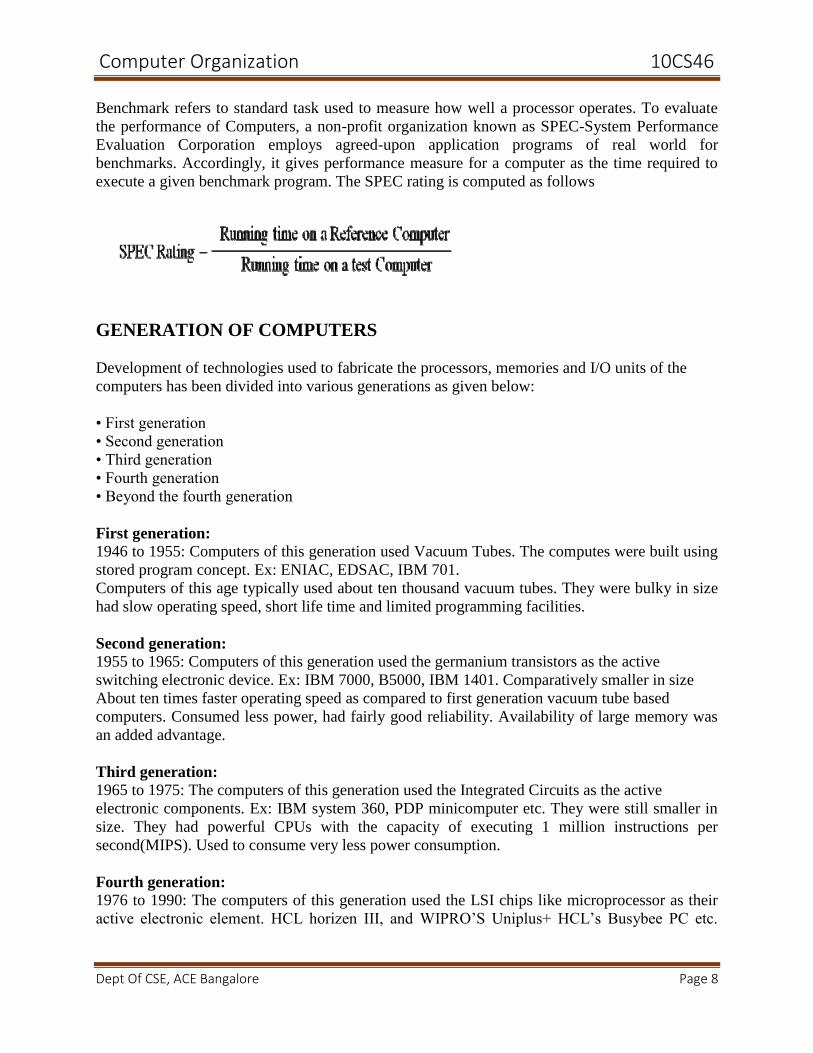
USER PROGRAM and OS ROUTINE INTERACTION
Let’s assume computer with 1 processor, 1 disk and 1 printer and application program is in
machine code on disk. The various tasks are performed in a coordinated fashion, which is
calledmultitasking. t0, t1 …t5 are the instances of time and the interaction during various
instances asgiven below:
t0: the OS loads the program from the disk to memory
t1: program executes
t2: program accesses disk
t3: program executes some more
t4: program accesses printer
t5: program terminates
Computer Organization 10CS46
Dept Of CSE, ACE Bangalore Page 7
Figure 6 :User program and OS routine sharing of the processor
PERFORMANCE
The total time required to execute a program is the most important measure of performance for a
computer. (t0-t5 of earlier example). Compiler, instruction set and hardware architecture,
program all have impact on performance.
Basic Performance Equation: The basic performance equation is given by
T = (N * S) / R
where T=execution time, N=number of instructions, S=average cycles per instruction, R=clock
rate in cycles per second
CACHING Commonly used data are copied to on-processor memory (cache) to reduce access time.
Small memories can be made with higher speed than large ones. In a computer, we need both.
Figure 7: The processor cache
PERFORMANCE MEASUREMENT
Computer Organization 10CS46
Dept Of CSE, ACE Bangalore Page 8
Benchmark refers to standard task used to measure how well a processor operates. To evaluate
the performance of Computers, a non-profit organization known as SPEC-System Performance
Evaluation Corporation employs agreed-upon application programs of real world for
benchmarks. Accordingly, it gives performance measure for a computer as the time required to
execute a given benchmark program. The SPEC rating is computed as follows
GENERATION OF COMPUTERS
Development of technologies used to fabricate the processors, memories and I/O units of the
computers has been divided into various generations as given below:
• First generation
• Second generation
• Third generation
• Fourth generation
• Beyond the fourth generation
First generation:
1946 to 1955: Computers of this generation used Vacuum Tubes. The computes were built using
stored program concept. Ex: ENIAC, EDSAC, IBM 701.
Computers of this age typically used about ten thousand vacuum tubes. They were bulky in size
had slow operating speed, short life time and limited programming facilities.
Second generation:
1955 to 1965: Computers of this generation used the germanium transistors as the active
switching electronic device. Ex: IBM 7000, B5000, IBM 1401. Comparatively smaller in size
About ten times faster operating speed as compared to first generation vacuum tube based
computers. Consumed less power, had fairly good reliability. Availability of large memory was
an added advantage.
Third generation:
1965 to 1975: The computers of this generation used the Integrated Circuits as the active
electronic components. Ex: IBM system 360, PDP minicomputer etc. They were still smaller in
size. They had powerful CPUs with the capacity of executing 1 million instructions per
second(MIPS). Used to consume very less power consumption.
Fourth generation:
1976 to 1990: The computers of this generation used the LSI chips like microprocessor as their
active electronic element. HCL horizen III, and WIPRO’S Uniplus+ HCL’s Busybee PC etc.
Computer Organization 10CS46
Dept Of CSE, ACE Bangalore Page 9
They used high speed microprocessor as CPU. They were more user friendly and highly reliable
systems. They had large storage capacity disk memories.
Beyond Fourth Generation:
1990 onwards: Specialized and dedicated VLSI chips are used to control specific functions of
these computers. Modern Desktop PC’s, Laptops or Notebook Computers.
Unit II:
Computer Organization 10CS46
Dept Of CSE, ACE Bangalore Page 10
MACHINE INSTRUCTIONS and PROGRAMS
This unit deals with concepts as to how programs are executed in the computer from the
machineinstruction set viewpoint. All computers deal with numbers. They have instructions that
performoperations on the data operands. Hence we start with basic Number systems.
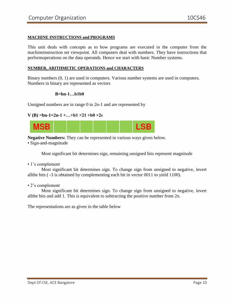
NUMBER, ARITHMETIC OPERATIONS and CHARACTERS
Binary numbers (0, 1) are used in computers. Various number systems are used in computers.
Numbers in binary are represented as vectors
B=bn-1…b1b0
Unsigned numbers are in range 0 to 2n-1 and are represented by
V (B) =bn-1×2n-1 +…+b1 ×21 +b0 ×20
Negative Numbers: They can be represented in various ways given below.
• Sign-and-magnitude
Most significant bit determines sign, remaining unsigned bits represent magnitude
• 1’s complement
Most significant bit determines sign. To change sign from unsigned to negative, invert
allthe bits ( -3 is obtained by complementing each bit in vector 0011 to yield 1100).
• 2’s complement
Most significant bit determines sign. To change sign from unsigned to negative, invert
allthe bits and add 1. This is equivalent to subtracting the positive number from 2n.
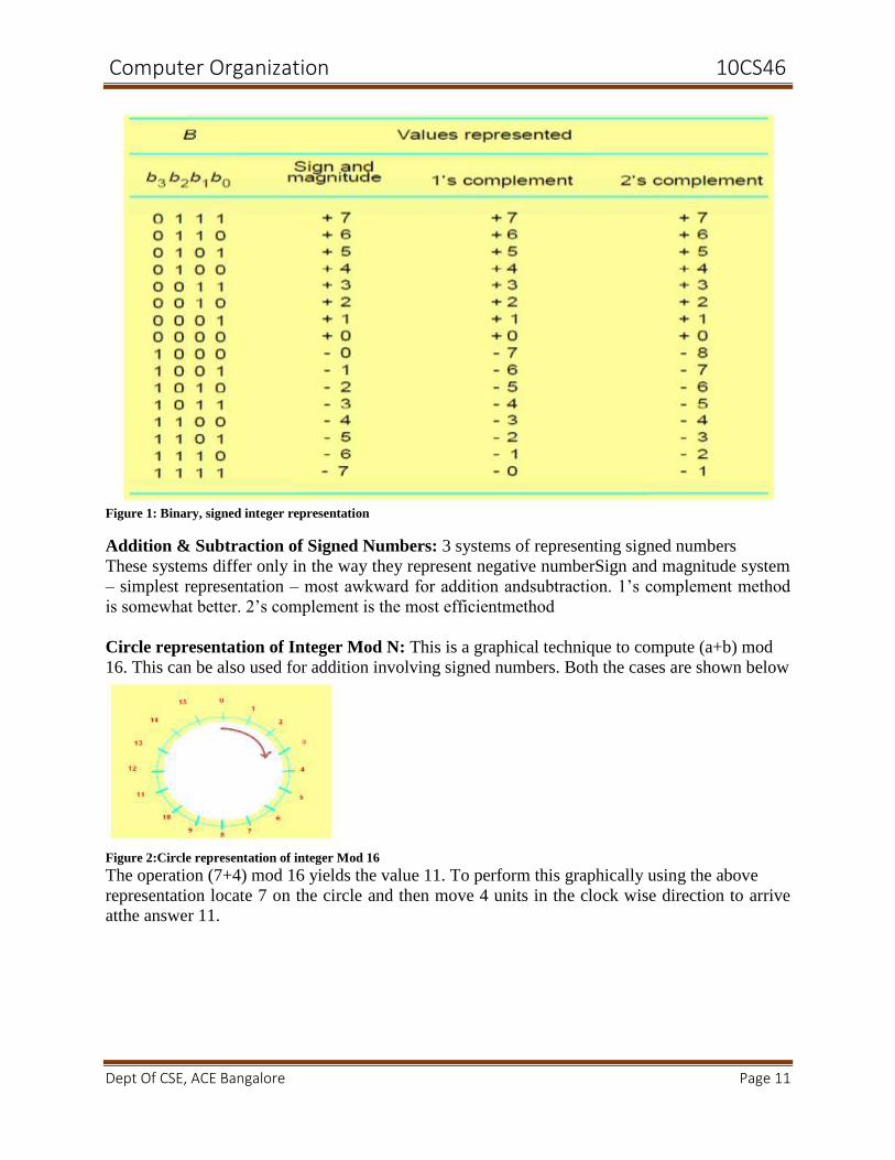
The representations are as given in the table below
Computer Organization 10CS46
Dept Of CSE, ACE Bangalore Page 11
Figure 1: Binary, signed integer representation
Addition & Subtraction of Signed Numbers: 3 systems of representing signed numbers
These systems differ only in the way they represent negative numberSign and magnitude system
– simplest representation – most awkward for addition andsubtraction. 1’s complement method
is somewhat better. 2’s complement is the most efficientmethod
Circle representation of Integer Mod N: This is a graphical technique to compute (a+b) mod
16. This can be also used for addition involving signed numbers. Both the cases are shown below
Figure 2:Circle representation of integer Mod 16
The operation (7+4) mod 16 yields the value 11. To perform this graphically using the above
representation locate 7 on the circle and then move 4 units in the clock wise direction to arrive
atthe answer 11.
Computer Organization 10CS46
Dept Of CSE, ACE Bangalore Page 12
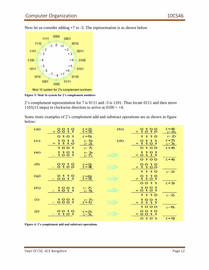
Next let us consider adding +7 to -3. The representation is as shown below
Figure 3: Mod 16 system for 2’s complement numbers
2’s complement representation for 7 is 0111 and -3 is 1101. Thus locate 0111 and then move
1101(13 steps) in clockwise direction to arrive at 0100 = +4.
Some more examples of 2’s complement add and substract operations are as shown in figure
below:
Figure 4: 2’s complement add and substract operations
Computer Organization 10CS46
Dept Of CSE, ACE Bangalore Page 13
Overflow in integer arithematic: In 2’s complement arithmetic addition of opposite sign
numbers will never result in overflow . If the numbers are the same sign and theresult is the
opposite sign, overflow has occurred.E.g. 0100 + 0111 =1011 (but 1011 is -5)
In case of unsigned numbers carry out signals that an overflow has occurred
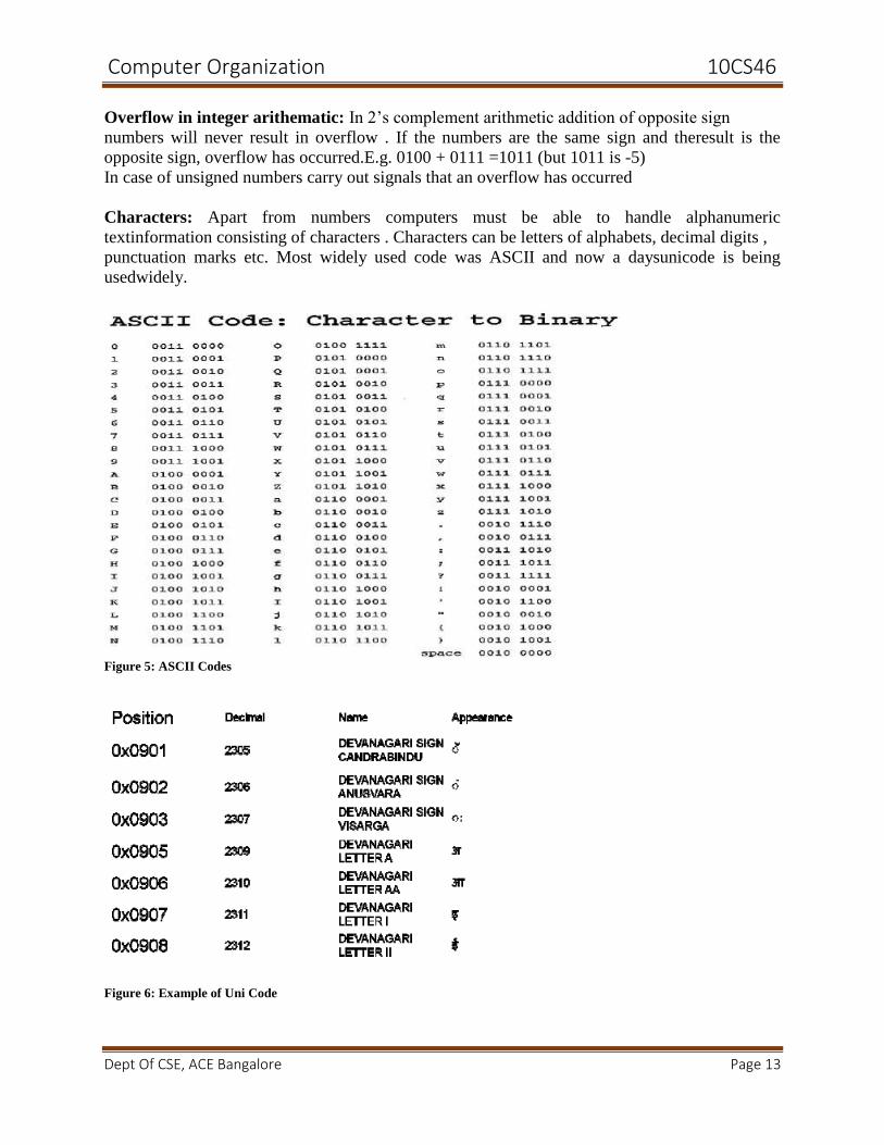
Characters: Apart from numbers computers must be able to handle alphanumeric
textinformation consisting of characters . Characters can be letters of alphabets, decimal digits ,
punctuation marks etc. Most widely used code was ASCII and now a daysunicode is being
usedwidely.
Figure 5: ASCII Codes
Figure 6: Example of Uni Code
Computer Organization 10CS46
Dept Of CSE, ACE Bangalore Page 14
MEMORY LOCATIONS and ADDRESSES Memory consists of storage cells. They store the bits 0 or 1. We can deal with them in n-bit
groups called words (typically 8, 16, 32 or 64 bits). Usually refer to memory size in bytes e.g.
we say we have 128MB memory and rarely use words as the unit. We use addresses to store
orretrieve item of information For some k, memory consists of 2k unique addresses which
rangefrom 0 to 2k -1. The possible addresses are the address space of the computer. E.g. 24-bit
addresshas 2 24 (16,777,216) locations. Information quantities: bit, byte, word where Byte=8 bits,
wordtypically varies 16-64 bits. Most machines address memory in units of bytes. For a 32-
bitmachine, successive words are at address 0, 4, 8, 12 and so on.
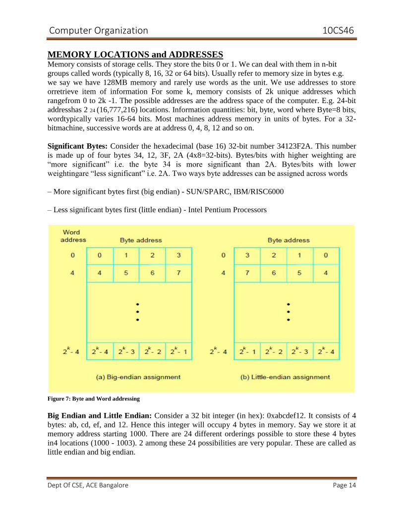
Significant Bytes: Consider the hexadecimal (base 16) 32-bit number 34123F2A. This number
is made up of four bytes 34, 12, 3F, 2A (4x8=32-bits). Bytes/bits with higher weighting are
“more significant” i.e. the byte 34 is more significant than 2A. Bytes/bits with lower
weightingare “less significant” i.e. 2A. Two ways byte addresses can be assigned across words
– More significant bytes first (big endian) - SUN/SPARC, IBM/RISC6000
– Less significant bytes first (little endian) - Intel Pentium Processors
Figure 7: Byte and Word addressing
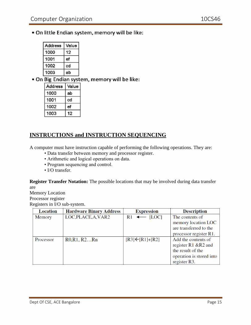
Big Endian and Little Endian: Consider a 32 bit integer (in hex): 0xabcdef12. It consists of 4
bytes: ab, cd, ef, and 12. Hence this integer will occupy 4 bytes in memory. Say we store it at
memory address starting 1000. There are 24 different orderings possible to store these 4 bytes
in4 locations (1000 - 1003). 2 among these 24 possibilities are very popular. These are called as
little endian and big endian.
Computer Organization 10CS46
Dept Of CSE, ACE Bangalore Page 15
INSTRUCTIONS and INSTRUCTION SEQUENCING
A computer must have instruction capable of performing the following operations. They are:
• Data transfer between memory and processor register.
• Arithmetic and logical operations on data.
• Program sequencing and control.
• I/O transfer.
Register Transfer Notation: The possible locations that may be involved during data transfer
are
Memory Location
Processor register
Registers in I/O sub-system.
Computer Organization 10CS46
Dept Of CSE, ACE Bangalore Page 16
Assembly Language Notation:
Basic Instruction Type:
INSTRUCTION EXECUTION and STRAIGHT LINE SEQUENCING
Instruction Execution: There are 2 phases for executing an instruction. They are,
• Instruction Fetch
• Instruction Execution
Instruction Fetch:
The instruction is fetched from the memory location whose address is in PC. This is then placed
in IR.
Instruction Execution:
Instruction in IR is examined and decoded to determine which operation is to be performed.
Program execution Steps:
To begin executing a program, the address of first instruction must be placed in PC.The
processor control circuits use the information in the PC to fetch & execute instructions one
at a time in the order of increasing order.
This is called Straight line sequencing. During the execution of each instruction, the PC is
incremented by 4 to point to the address of next instruction.
Computer Organization 10CS46
Dept Of CSE, ACE Bangalore Page 17
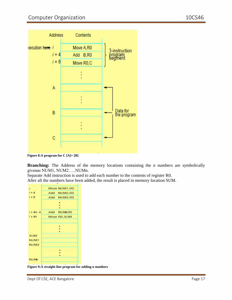
Figure 8:A program for C [A]+ [B]
Branching: The Address of the memory locations containing the n numbers are symbolically
givenas NUM1, NUM2…..NUMn.
Separate Add instruction is used to add each number to the contents of register R0.
After all the numbers have been added, the result is placed in memory location SUM.
Figure 9:A straight line program for adding n numbers
Computer Organization 10CS46
Dept Of CSE, ACE Bangalore Page 18
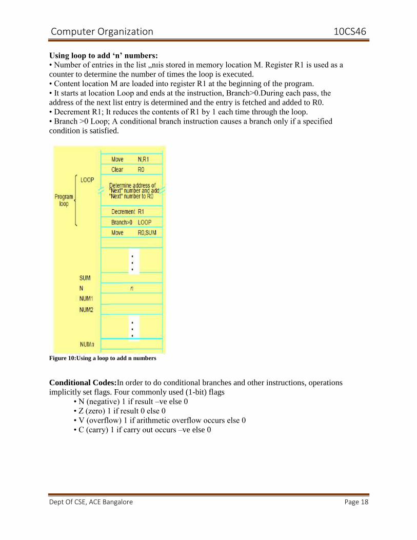
Using loop to add ‘n’ numbers:
• Number of entries in the list „nıis stored in memory location M. Register R1 is used as a
counter to determine the number of times the loop is executed.
• Content location M are loaded into register R1 at the beginning of the program.
• It starts at location Loop and ends at the instruction, Branch>0.During each pass, the
address of the next list entry is determined and the entry is fetched and added to R0.
• Decrement R1; It reduces the contents of R1 by 1 each time through the loop.
• Branch >0 Loop; A conditional branch instruction causes a branch only if a specified
condition is satisfied.
Figure 10:Using a loop to add n numbers
Conditional Codes:In order to do conditional branches and other instructions, operations
implicitly set flags. Four commonly used (1-bit) flags
• N (negative) 1 if result –ve else 0
• Z (zero) 1 if result 0 else 0
• V (overflow) 1 if arithmetic overflow occurs else 0
• C (carry) 1 if carry out occurs –ve else 0
Computer Organization 10CS46
Dept Of CSE, ACE Bangalore Page 19
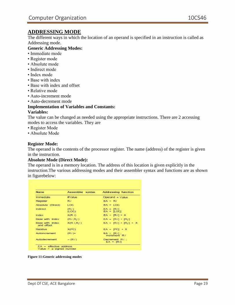
ADDRESSING MODE The different ways in which the location of an operand is specified in an instruction is called as
Addressing mode.
Generic Addressing Modes:
• Immediate mode
• Register mode
• Absolute mode
• Indirect mode
• Index mode
• Base with index
• Base with index and offset
• Relative mode
• Auto-increment mode
• Auto-decrement mode
Implementation of Variables and Constants:
Variables:
The value can be changed as needed using the appropriate instructions. There are 2 accessing
modes to access the variables. They are
• Register Mode
• Absolute Mode
Register Mode:
The operand is the contents of the processor register. The name (address) of the register is given
in the instruction.
Absolute Mode (Direct Mode):
The operand is in a memory location. The address of this location is given explicitly in the
instruction.The various addressing modes and their assembler syntax and functions are as shown
in figurebelow:
Figure 11:Generic addressing modes
Computer Organization 10CS46
Dept Of CSE, ACE Bangalore Page 20
Immediate Addressing Mode: The operand is specified in the instruction itself .
Move 200immediate, R0
Move #200, R0
Direct Addressing Mode: Operand resides in Memory and its address is given explicitly in the
address field of an instruction.
Move P, R0
Move R0, S
Add Q, R0
Register Addressing Mode: name of the register (address code of a specific general purpose
register) appears in the address field of an instruction i.e.
Move B, R1
Indexing and Arrays:
Index Mode:
The effective address of an operand is generated by adding a constant value to the contents of
aregister. The constant value uses either special purpose or general purpose register.
X (RI)
whereX – denotes the constant value contained in the instruction
Ri– name of the register involved.
The Effective Address of the operand EA=X + [Ri]
The index register R1 contains the address of a new location and the value of X defines an offset
(also called a displacement).
To find operand first go to Reg R1 (using address)-read the content from R1 i.e. 1000
Add the content 1000 with offset 20 to get the result. Here the constant X refers to the new
address and the contents of index register that defines the offset to the operand.
The sum of two values is given explicitly in the instruction and the other is stored in register.
Add 20(R1), R2 (or) EA=>1000+20=1020
Relative Addressing: It is same as index mode. The difference is, instead of general purpose
register, here we can use program counter (PC).
Relative Mode:
The Effective Address is determined by the Index mode using the PC in place of the general
purpose register.
This mode can be used to access the data operand. But it’s most common use is to specify the
target address in branch instruction. Eg. Branch>0 Loop
It causes the program execution to go to the branch target location. It is identified by the name
loop if the branch condition is satisfied.
Additional Modes:
There are two additional modes. They are
• Auto-increment mode
• Auto-decrement mode
Computer Organization 10CS46
Dept Of CSE, ACE Bangalore Page 21
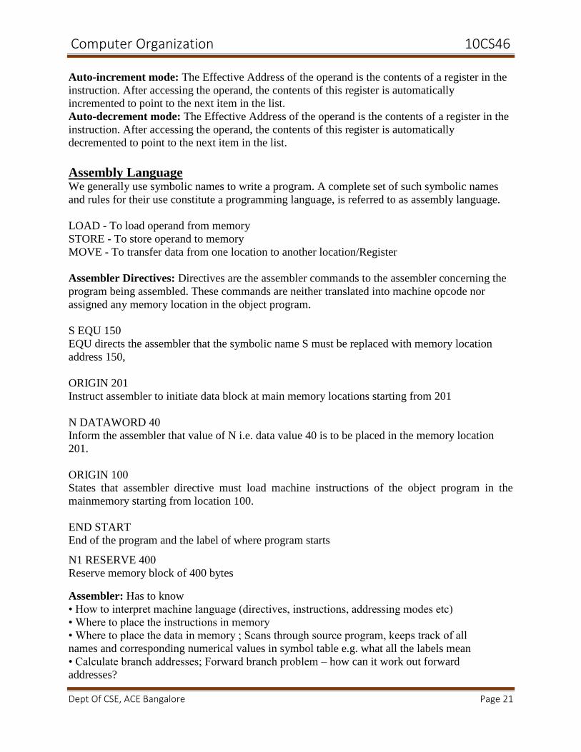
Auto-increment mode: The Effective Address of the operand is the contents of a register in the
instruction. After accessing the operand, the contents of this register is automatically
incremented to point to the next item in the list.
Auto-decrement mode: The Effective Address of the operand is the contents of a register in the
instruction. After accessing the operand, the contents of this register is automatically
decremented to point to the next item in the list.
Assembly Language We generally use symbolic names to write a program. A complete set of such symbolic names
and rules for their use constitute a programming language, is referred to as assembly language.
LOAD - To load operand from memory
STORE - To store operand to memory
MOVE - To transfer data from one location to another location/Register
Assembler Directives: Directives are the assembler commands to the assembler concerning the
program being assembled. These commands are neither translated into machine opcode nor
assigned any memory location in the object program.
S EQU 150
EQU directs the assembler that the symbolic name S must be replaced with memory location
address 150,
ORIGIN 201
Instruct assembler to initiate data block at main memory locations starting from 201
N DATAWORD 40
Inform the assembler that value of N i.e. data value 40 is to be placed in the memory location
201.
ORIGIN 100
States that assembler directive must load machine instructions of the object program in the
mainmemory starting from location 100.
END START
End of the program and the label of where program starts
N1 RESERVE 400
Reserve memory block of 400 bytes
Assembler: Has to know
• How to interpret machine language (directives, instructions, addressing modes etc)
• Where to place the instructions in memory
• Where to place the data in memory ; Scans through source program, keeps track of all
names and corresponding numerical values in symbol table e.g. what all the labels mean
• Calculate branch addresses; Forward branch problem – how can it work out forward
addresses?
Computer Organization 10CS46
Dept Of CSE, ACE Bangalore Page 22
Two Pass Assembler:
• First pass
– Work out all the addresses of labels
• Second pass
– Generate machine code, substituting values for the labels
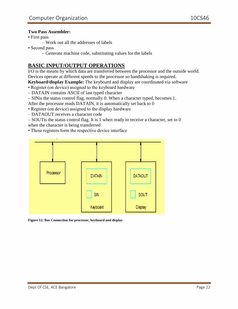
BASIC INPUT/OUTPUT OPERATIONS I/O is the means by which data are transferred between the processor and the outside world.
Devices operate at different speeds to the processor so handshaking is required.
Keyboard/display Example: The keyboard and display are coordinated via software
• Register (on device) assigned to the keyboard hardware
– DATAIN contains ASCII of last typed character
– SINis the status control flag, normally 0. When a character typed, becomes 1.
After the processor reads DATAIN, it is automatically set back to 0
• Register (on device) assigned to the display hardware
– DATAOUT receives a character code
– SOUTis the status control flag. It is 1 when ready to receive a character, set to 0
when the character is being transferred
• These registers form the respective device interface
Figure 12: Bus Connection for processor, keyboard and display
Computer Organization 10CS46
Dept Of CSE, ACE Bangalore Page 23
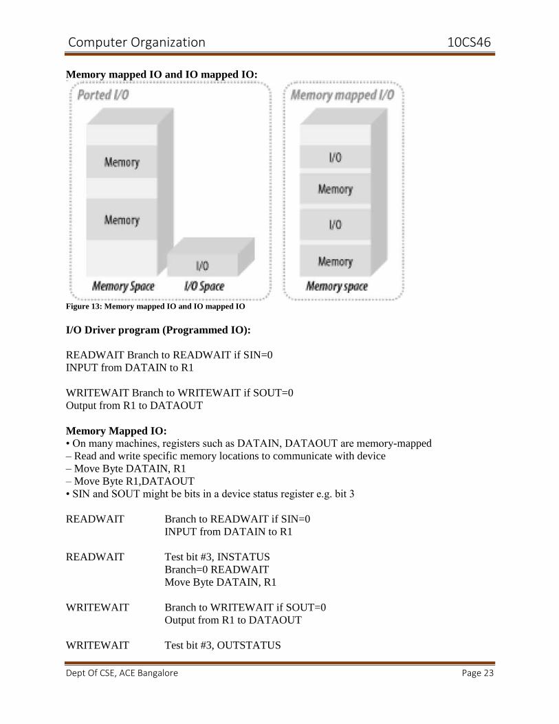
Memory mapped IO and IO mapped IO:
Figure 13: Memory mapped IO and IO mapped IO
I/O Driver program (Programmed IO):
READWAIT Branch to READWAIT if SIN=0
INPUT from DATAIN to R1
WRITEWAIT Branch to WRITEWAIT if SOUT=0
Output from R1 to DATAOUT
Memory Mapped IO:
• On many machines, registers such as DATAIN, DATAOUT are memory-mapped
– Read and write specific memory locations to communicate with device
– Move Byte DATAIN, R1
– Move Byte R1,DATAOUT
• SIN and SOUT might be bits in a device status register e.g. bit 3
READWAIT Branch to READWAIT if SIN=0
INPUT from DATAIN to R1
READWAIT Test bit #3, INSTATUS
Branch=0 READWAIT
Move Byte DATAIN, R1
WRITEWAIT Branch to WRITEWAIT if SOUT=0
Output from R1 to DATAOUT
WRITEWAIT Test bit #3, OUTSTATUS
Computer Organization 10CS46
Dept Of CSE, ACE Bangalore Page 24
Branch=0 WRITEWAIT
Move Byte R1, DATAOUT
Program to read a line of character and display it :
Move #LOC,R0 Initialize pointer register R0 to point to
the address of the first location in memory
where the characters are to be stored.
READ TestBit #3,INSTATUS Wait for a character to be entered
Branch=0 READ in the keyboard buffer DATAIN.
MoveByte DATAIN,(R0) Transfer the character from DATAIN into
the memory (this clears SIN to 0)
ECHO TestBit #3, OUTSTATUS Wait for the display to become ready.
Branch=0 ECHO
MoveByte (R0),DATAOUT Move the character just read to the display
buffer register (this clears SOUT to 0).
Compare #CR,(R0)+ Check if the character just read is CR
(carriage return). If it is not CR, then
Branch_0 READ branch back and read another character.
Also, increment the pointer to store the next
character.
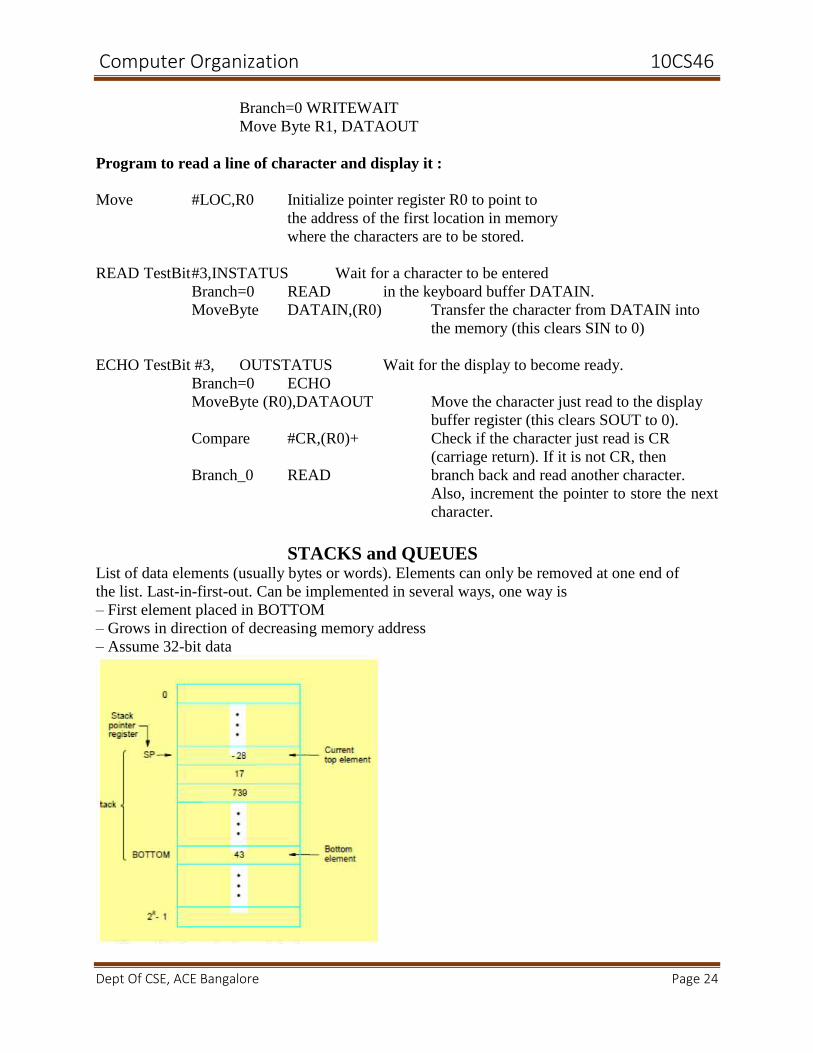
STACKS and QUEUES List of data elements (usually bytes or words). Elements can only be removed at one end of
the list. Last-in-first-out. Can be implemented in several ways, one way is
– First element placed in BOTTOM
– Grows in direction of decreasing memory address
– Assume 32-bit data
Computer Organization 10CS46
Dept Of CSE, ACE Bangalore Page 25
Figure 14: A stack of words in the memory
Stack Implementation:
Subtract #4, SP
Move NEWITEM,(SP) ; push
Move (SP), ITEM; pop
Add #4, SP
With auto increment and auto decrement
Move NEWITEM,-(SP); push
Move (SP) +, ITEM; pop
Queue:
• First-in-first-out
• Unlike a stack, need to keep track of both the front and end for removal and insertion
respectively
• Need two pointers to keep track of both ends
• Assuming it moves through memory in direction of higher addresses, as it is used, it
walks through memory towards higher addresses.
Circular buffers:
• Avoid this problem by limiting to a fixed region in memory
• Start at BEGINNING and entries appended until it reaches END after which it wraps
back around to BEGINNING
• Need to deal with cases when it is completely full and completely empty
SUBROUTINES • Often need to perform subtask on different data we use subtask called a subroutine
• Rather than include the same sequence of instructions everywhere it is needed, call a
subroutine instead
– One copy of subroutine stored in memory
– Subroutine call causes a branch to the subroutine
– At the end of the subroutine, a return instruction is executed
– Program resumes execution at the instruction immediately following the subroutine call
Parameter Passing:
Subroutine call
– e.g. SUM = listadd (N, NUM);
– N is a variable in memory and NUM is an address pointing to the start of the NUM list
– How do we send the parameters N, NUM to the subroutine?
– How do we receive the return value SUM?
One way is putting the parameters in registers; second way is Passing Parameters on stack and
third way is passing by value and reference.
CISC & RISC • Multiple length instructions are difficult to implement with high clock rate
Computer Organization 10CS46
Dept Of CSE, ACE Bangalore Page 26
• Complex instruction set computers (CISC) have complex instruction encodings like this (e.g.
IA-32)
• Reduced instruction set computers (RISC) only allow simple 32-bit formats, few addressing
modes and all data to be manipulated must be in registers e.g. Add (R3),R2 is not allowed,
instead use Move (R3),R1 followed by Add R1,R2 (e.g. ARM)
RISC machines often are 3-address machines as the addressing mode field is either not necessary
or simplified e.g. Add R1, R2, R3
• CISC machines usually require less instructions but have a lower clock rate, RISC require more
instructions but have a higher clock rate.
Computer Organization 10CS46
Dept Of CSE, ACE Bangalore Page 27
Unit 3 and Unit 4:
INPUT/OUTPUT ORGANIZATION
A general purpose computer should have the ability to exchange information with a wide range of devices
in varying environments. Computers can communicate with other computers over the Internet and access
information around the globe. They are an integral part of home appliances, manufacturing equipment,
transportation systems, banking and point-of-sale terminals. In this chapter, we study the various ways in
which I/O operations are performed.
Accessing I/O Devices
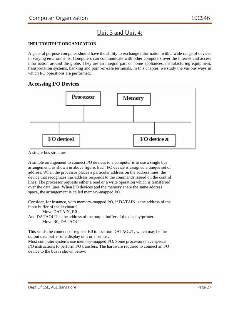
A single-bus structure
A simple arrangement to connect I/O devices to a computer is to use a single bus
arrangement, as shown in above figure. Each I/O device is assigned a unique set of
address. When the processor places a particular address on the address lines, the
device that recognizes this address responds to the commands issued on the control
lines. The processor requests either a read or a write operation which is transferred
over the data lines. When I/O devices and the memory share the same address
space, the arrangement is called memory-mapped I/O.
Consider, for instance, with memory-mapped I/O, if DATAIN is the address of the
input buffer of the keyboard
Move DATAIN, R0
And DATAOUT is the address of the output buffer of the display/printer
Move R0, DATAOUT
This sends the contents of register R0 to location DATAOUT, which may be the
output data buffer of a display unit or a printer.
Most computer systems use memory-mapped I/O. Some processors have special
I/O instructions to perform I/O transfers. The hardware required to connect an I/O
device to the bus is shown below:
Computer Organization 10CS46
Dept Of CSE, ACE Bangalore Page 28
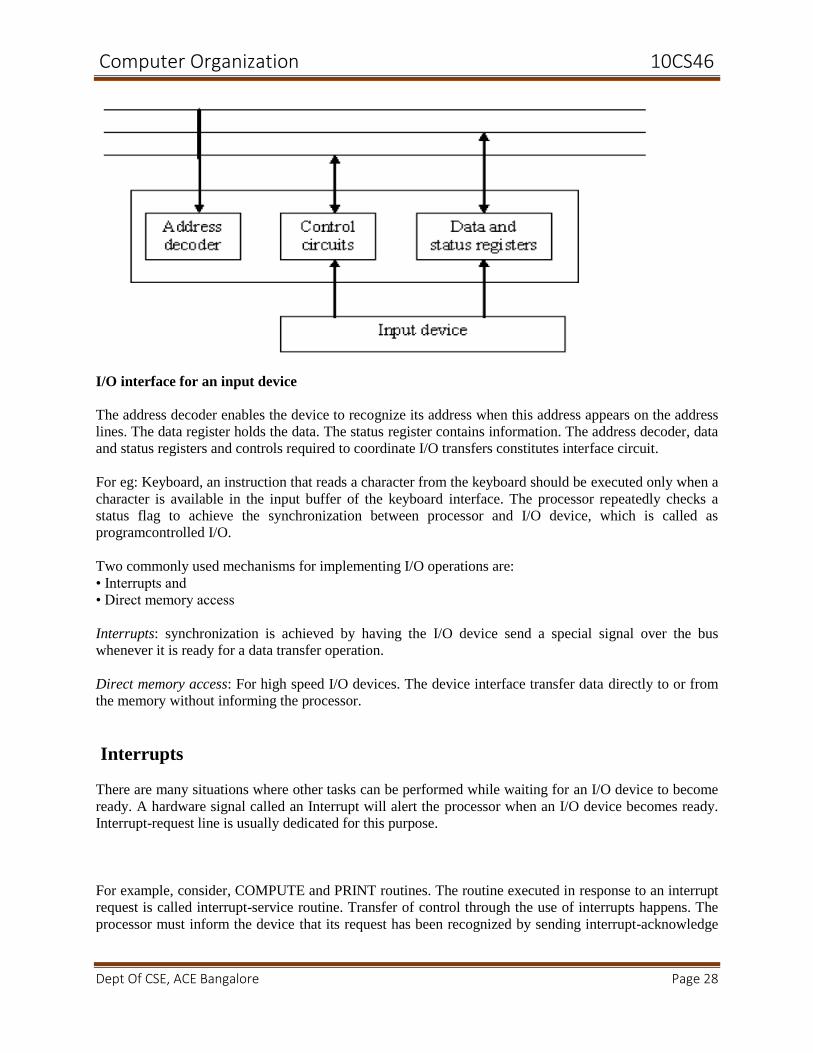
I/O interface for an input device
The address decoder enables the device to recognize its address when this address appears on the address
lines. The data register holds the data. The status register contains information. The address decoder, data
and status registers and controls required to coordinate I/O transfers constitutes interface circuit.
For eg: Keyboard, an instruction that reads a character from the keyboard should be executed only when a
character is available in the input buffer of the keyboard interface. The processor repeatedly checks a
status flag to achieve the synchronization between processor and I/O device, which is called as
programcontrolled I/O.
Two commonly used mechanisms for implementing I/O operations are:
• Interrupts and
• Direct memory access
Interrupts: synchronization is achieved by having the I/O device send a special signal over the bus
whenever it is ready for a data transfer operation.
Direct memory access: For high speed I/O devices. The device interface transfer data directly to or from
the memory without informing the processor.
Interrupts
There are many situations where other tasks can be performed while waiting for an I/O device to become
ready. A hardware signal called an Interrupt will alert the processor when an I/O device becomes ready.
Interrupt-request line is usually dedicated for this purpose.
For example, consider, COMPUTE and PRINT routines. The routine executed in response to an interrupt
request is called interrupt-service routine. Transfer of control through the use of interrupts happens. The
processor must inform the device that its request has been recognized by sending interrupt-acknowledge
Computer Organization 10CS46
Dept Of CSE, ACE Bangalore Page 29
signal. One must therefore know the difference between Interrupt Vs Subroutine. Interrupt latencyis
concerned with saving information in registers will increase the delay
between the time an interrupt request is received and the start of execution of the interrupt-service routine.
Interrupt hardware
Most computers have several I/O devices that can request an interrupt. A single interrupt request line may
be used to serve n devices.
Enabling and Disabling Interrupts
All computers fundamentally should be able to enable and disable interruptions as desired. Again
reconsider the COMPUTE and PRINT example. When a device activates the interrupt-request signal, it
keeps this signal activated until it learns that the processor has accepted its request. When interrupts are
enabled, the following is a typical scenario:
• The device raises an interrupt request.
• The processor interrupts the program currently being executed.
• Interrupts are disabled by changing the control bits in the processor status
register (PS).
• The device is informed that its request has been recognized and deactivates
the interrupt request signal.
• The action requested by the interrupt is performed by the interrupt-service
routine.
• Interrupts are enabled and execution of the interrupted program is
Resumed
Handling multiple devices
While handling multiple devices, the issues concerned are:
• How can the processor recognize the device requesting an interrupt?
• How can the processor obtain the starting address of the appropriate routine?
• Should a device be allowed to interrupt the processor while another interrupt
is being serviced?
• How should two or more simultaneous interrupt requests be handled?
Vectored interrupts
A device requesting an interrupt may identify itself (by sending a special
code) directly to the processor, so that the processor considers it immediately.
Interrupt nesting
The processor should continue to execute the interrupt-service routine till completion, before it accepts an
interrupt request from a second device. Privilege exception means they execute privileged instructions.
Individual interrupt-request and acknowledge lines can also be implemented. Implementation of interrupt
priority using individual interrupt-request and acknowledge lines has been shown in figure 4.7.
Simultaneous requests
Computer Organization 10CS46
Dept Of CSE, ACE Bangalore Page 30
The processor must have some mechanisms to decide which request to
service when simultaneous requests arrive. Here, daisy chain and arrangement of
priority groups as the interrupt priority schemes are discussed. Priority based
simultaneous requests are considered in many organizations.
Controlling device requests
At the device end, an interrupt enable bit determines whether it is allowed to
generate an interrupt request. At the processor end, it determines whether a given
interrupt request will be accepted.
Exceptions
The term exception is used to refer to any event that causes an interruption.
Hence, I/O interrupts are one example of an exception.
• Recovery from errors – These are techniques to ensure that all hardware
components are operating properly.
• Debugging – find errors in a program, trace and breakpoints (only at specific
points selected by the user).
• Privilege exception – execute privileged instructions to protect OS of a
computer.
Use of interrupts in Operating Systems
Operating system is system software which is also termed as resource manager, as it manages all variety
of computer peripheral devices efficiently.
Different issues addressed by the operating systems are: Assign priorities among jobs, Security and
protection features, incorporate interrupt-service routines for all devices and Multitasking, time slice,
process, program state, context switch and others.
Direct Memory Access
As we have seen earlier, the two commonly used mechanisms for implementing I/O operations are:
• Interrupts and
• Direct memory access
Interrupts: synchronization is achieved by having the I/O device send a special signal over the bus
whenever it is ready for a data transfer operation Direct memory access:
Basically for high speed I/O devices, the device interface transfer data directly to or from the memory
without informing the processor. When interrupts are used, additional overhead involved with saving and
restoring the program counter and other state information. To transfer large blocks of data at high speed,
an alternative approach is used. A special control unit will allow transfer of a block of data directly
between an external device and the main memory, without continuous intervention
by the processor.
DMA controller is a control circuit that performs DMA transfers, is a part of the I/O device interface. It
performs functions that normally be carried out by the processor. DMA controller must increment the
Computer Organization 10CS46
Dept Of CSE, ACE Bangalore Page 31
memory address and keep track of the number of transfers. The operations of DMA controller must be
under the control of a program executed by the processor. To initiate the transfer of block of words, the
processor sends the starting address, the number of words in the block and the direction of the transfer.
On receiving this information, DMA controller transfers the entire block and informs the processor by
raising an interrupt signal. While a DMA transfer is taking place, the processor can be used to execute
another program. After the DMA transfer is completed, the processor can return to the program that
requested the transfer.
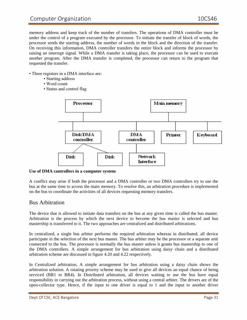
• Three registers in a DMA interface are:
• Starting address
• Word count
• Status and control flag
Use of DMA controllers in a computer system
A conflict may arise if both the processor and a DMA controller or two DMA controllers try to use the
bus at the same time to access the main memory. To resolve this, an arbitration procedure is implemented
on the bus to coordinate the activities of all devices requesting memory transfers.
Bus Arbitration
The device that is allowed to initiate data transfers on the bus at any given time is called the bus master.
Arbitration is the process by which the next device to become the bus master is selected and bus
mastership is transferred to it. The two approaches are centralized and distributed arbitrations.
In centralized, a single bus arbiter performs the required arbitration whereas in distributed, all device
participate in the selection of the next bus master. The bus arbiter may be the processor or a separate unit
connected to the bus. The processor is normally the bus master unless it grants bus mastership to one of
the DMA controllers. A simple arrangement for bus arbitration using daisy chain and a distributed
arbitration scheme are discussed in figure 4.20 and 4.22 respectively.
In Centralized arbitration, A simple arrangement for bus arbitration using a daisy chain shows the
arbitration solution. A rotating priority scheme may be used to give all devices an equal chance of being
serviced (BR1 to BR4). In Distributed arbitration, all devices waiting to use the bus have equal
responsibility in carrying out the arbitration process, without using a central arbiter. The drivers are of the
open-collector type. Hence, if the input to one driver is equal to 1 and the input to another driver
Computer Organization 10CS46
Dept Of CSE, ACE Bangalore Page 32
connected to the same bus line is equal to 0 the bus will be in the low-voltage state. This uses ARB0 to
ARB3.
Buses
The Primary function of the bus is to provide a communication path for the transfer of data. It must also
look in to,
– When to place information on the bus?
– When to have control signals?
Some bus protocols are set. These involve data, address and control lines. A variety
of schemes have been devised for the timing of data transfers over a bus. They are:
Synchronous and Asynchronous schemes
Bus master is an initiator. Usually, processor acts as master. But under DMA setup, any other device can
be master. The device addressed by the master is slave or target.
Synchronous bus
All devices derive timing information from a common clock line. Equallyspaced pulses on this line define
equal time intervals. Each of these intervalsconstitutes a bus cycle during which one data transfer can take
place. Timing of aninput/output transfer on a synchronous bus is shown in figure 4.23.
Asynchronous bus This is a scheme based on the use of a handshake between the master andthe slave for controlling data
transfers on the bus. The common clock is replaced bytwo timing control lines, master-ready and slave-
ready. The first is asserted by themaster to indicate that it is ready for a transaction and the second is a
response from the slave. The master places the address and command information on the bus. It indicates
to all devices that it has done so by activating the master-ready line. This causes all devices on the bus to
decode the address. The selected slave performs the required operation and informs the processor it has
done so by activating the slave ready line. A typical handshake control of data transfer during an input
and an output operations are shown in figure 4.26 and 4.27 respectively. The master waits for slave-ready
to become asserted before it removes its signals from the bus. The
handshake signals are fully interlocked. A change of state in one signal is followed bya change in the
other signal. Hence this scheme is known as a full handshake.
Interface Circuits
An I/O interface consists of the circuitry required to connect an I/O device to a computer bus. On one side
of the interface, we have bus signals. On the other side, we have a data path with its associated controls to
transfer data between the interface and the I/O device – port. We have two types:
Serial port and
Parallel port
A parallel port transfers data in the form of a number of bits (8 or 16)simultaneously to or from the
device. A serial port transmits and receives data one bit at a time. Communication with the bus is the
same for both formats. The conversion from the parallel to the serial format, and vice versa, takes place
inside the interface circuit. In parallel port, the connection between the device and the computer uses a
multiple-pin connector and a cable with as many wires. This arrangement is suitable for devices that are
Computer Organization 10CS46
Dept Of CSE, ACE Bangalore Page 33
physically close to the computer. In serial port, it is much more convenient and cost-effective where
longer cables are needed.
Typically, the functions of an I/O interface are:
• Provides a storage buffer for at least one word of data
• Contains status flags that can be accessed by the processor to determinewhether the buffer is full
or empty
• Contains address-decoding circuitry to determine when it is being addressed
by the processor
• Generates the appropriate timing signals required by the bus control scheme
• Performs any format conversion that may be necessary to transfer data
between the bus and the I/O device, such as parallel-serial conversion in the
case of a serial port
Parallel Port
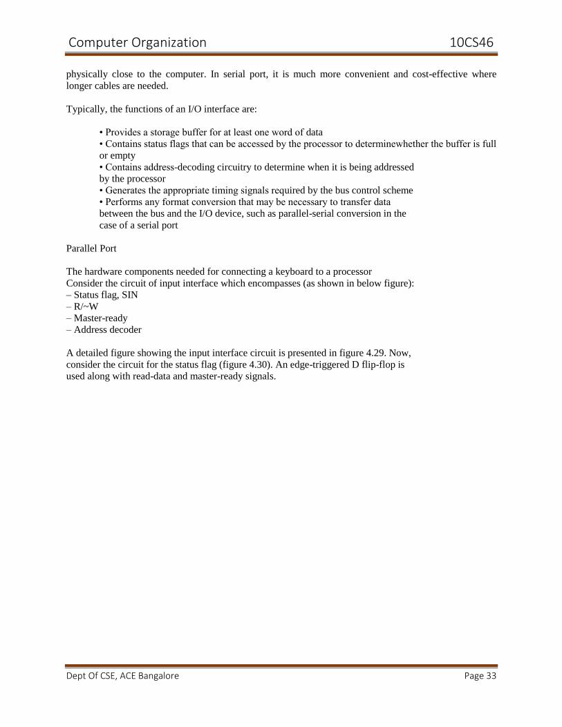
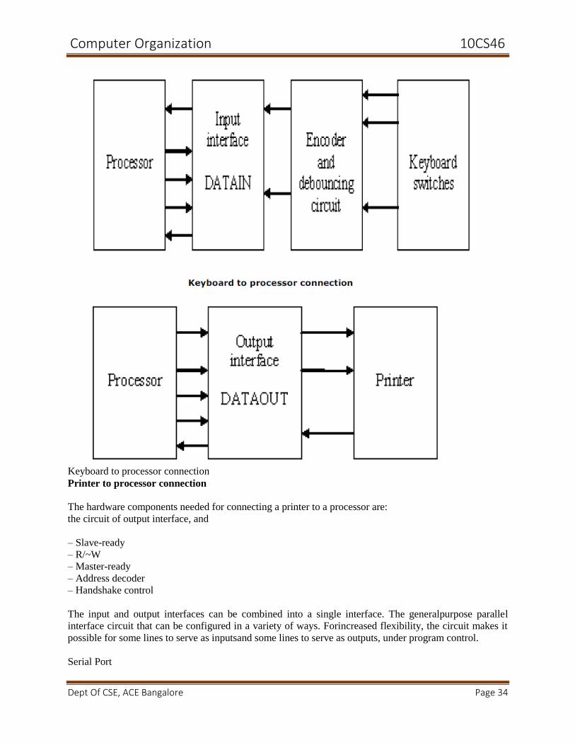
The hardware components needed for connecting a keyboard to a processor
Consider the circuit of input interface which encompasses (as shown in below figure):
– Status flag, SIN
– R/~W
– Master-ready
– Address decoder
A detailed figure showing the input interface circuit is presented in figure 4.29. Now,
consider the circuit for the status flag (figure 4.30). An edge-triggered D flip-flop is
used along with read-data and master-ready signals.
Computer Organization 10CS46
Dept Of CSE, ACE Bangalore Page 34
Keyboard to processor connection
Printer to processor connection
The hardware components needed for connecting a printer to a processor are:
the circuit of output interface, and
– Slave-ready
– R/~W
– Master-ready
– Address decoder
– Handshake control
The input and output interfaces can be combined into a single interface. The generalpurpose parallel
interface circuit that can be configured in a variety of ways. Forincreased flexibility, the circuit makes it
possible for some lines to serve as inputsand some lines to serve as outputs, under program control.
Serial Port
Computer Organization 10CS46
Dept Of CSE, ACE Bangalore Page 35
A serial interface circuit involves – Chip and register select, Status andcontrol, Output shift register,
DATAOUT, DATAIN, Input shift register and Serialinput/output – as shown in figure 4.37.
Standard I/O interfaces
Consider a computer system using different interface standards. Let us look in to Processor bus and
Peripheral Component Interconnect (PCI) bus. These two buses are interconnected by a circuit called
bridge. It is a bridge between processor bus and PCI bus. An example of a computer system using
different interface standards is shown in figure 4.38. The three major standard I/O interfaces discussed
here are:
– PCI (Peripheral Component Interconnect)
– SCSI (Small Computer System Interface)
– USB (Universal Serial Bus)
PCI (Peripheral Component Interconnect)
The topics discussed under PCI are: Data Transfer, Use of a PCI bus in a computer system, A read
operation on the PCI bus, Device configuration and Other electrical characteristics. Use of a PCI bus in a
computer system is shown in figure4.39 as a representation.
Host, main memory and PCI bridge are connected to disk, printer and Ethernet interface through PCI bus.
At any given time, one device is the bus master. It has the right to initiate data transfers by issuing read
and write commands. A master is called an initiator in PCI terminology. This is either processor or DMA
controller. The addressed device that responds to read and write commands is called a target. A complete
transfer operation on the bus, involving an address and a burst of data, is
called a transaction. Device configuration is also discussed.
SCSI Bus
It is a standard bus defined by the American National Standards Institute (ANSI).
A controller connected to a SCSI bus is an initiator or a target. The processor sends a
command to the SCSI controller, which causes the following sequence of events to
take place:
• The SCSI controller contends for control of the bus (initiator).
• When the initiator wins the arbitration process, it selects the target controller and hands over
control of the bus to it.
• The target starts an output operation. The initiator sends a command specifying the required
read operation.
• The target sends a message to the initiator indicating that it will temporarily suspends the
connection between them. Then it releases the bus.
• The target controller sends a command to the disk drive to move the read head to the first sector
involved in the requested read operation.
• The target transfers the contents of the data buffer to the initiator and then suspends the
connection again.
• The target controller sends a command to the disk drive to perform another seek operation.
• As the initiator controller receives the data, it stores them into the main memory using the DMA
approach.
Computer Organization 10CS46
Dept Of CSE, ACE Bangalore Page 36
• The SCSI controller sends an interrupt to the processor to inform it that the requested operation
has been completed.
The bus signals, arbitration, selection, information transfer and reselection are the
topics discussed in addition to the above.
Universal Serial Bus (USB)
The USB has been designed to meet several key objectives such as:
• Provide a simple, low-cost and easy to use interconnection system thatovercomes the difficulties
due to the limited number of I/O ports available ona computer
• Accommodate a wide range of data transfer characteristics for I/O devices,including telephone
and Internet connections
• Enhance user convenience through a “plug-and-play” mode of operation
Port Limitation
Here to add new ports, a user must open the computer box to gain access to theinternal expansion bus and
install a new interface card. The user may also need toknow how to configure the device and the software.
And also it is to make it possibleto add many devices to a computer system at any time, without opening
thecomputer box.
Device Characteristics
The kinds of devices that may be connected to a computer cover a wide range of functionality - speed,
volume and timing constraints. A variety of simple devices attached to a computer generate data in
different asynchronous mode. A signal must be sampled quickly enough to track its highest-frequency
components.
Plug-and-play
Whenever a device is introduced, do not turn the computer off/restart to connect/disconnect a device. The
system should detect the existence of this new device automatically, identify the appropriate device-driver
software and any other facilities needed to service that device, and establish the appropriate addresses and
logical connections to enable them to communicate.
USB architecture
To accommodate a large number of devices that can be added or removed at anytime, the USB has the
tree structure. Each node has a device called a hub. Root hub, functions, split bus operations – high speed
(HS) and Full/Low speed (F/LS).
Computer Organization 10CS46
Dept Of CSE, ACE Bangalore Page 37
Unit 5.
Memory Systems
Basic Concepts
The two primary classifications of memory are
1)Primary memory
2) Secondary memory
Under Primary memory the two classifications are
1)RAM (Random Accesses Memory)
2)ROM(Read Only Memory)
RAM :-Its is further classified into
a) Static RAM (SRAM)
b) Dynamic RAM(DRAM)
DRAM:-the Dynamic RAM is again further Sub Classified into
i) Synchronous DRAM
ii) Asynchronous DRAM
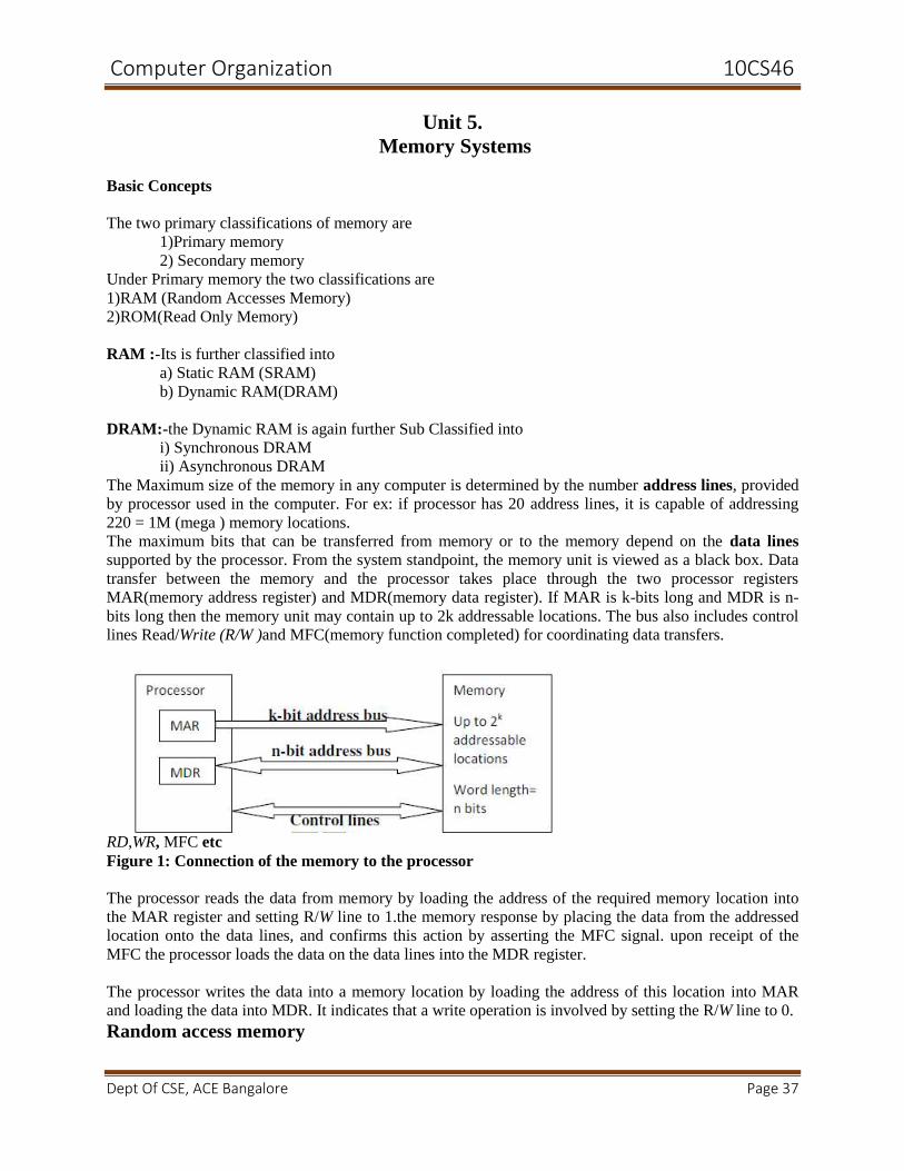
The Maximum size of the memory in any computer is determined by the number address lines, provided
by processor used in the computer. For ex: if processor has 20 address lines, it is capable of addressing
220 = 1M (mega ) memory locations.
The maximum bits that can be transferred from memory or to the memory depend on the data lines
supported by the processor. From the system standpoint, the memory unit is viewed as a black box. Data
transfer between the memory and the processor takes place through the two processor registers
MAR(memory address register) and MDR(memory data register). If MAR is k-bits long and MDR is n-
bits long then the memory unit may contain up to 2k addressable locations. The bus also includes control
lines Read/Write (R/W )and MFC(memory function completed) for coordinating data transfers.
RD,WR, MFC etc
Figure 1: Connection of the memory to the processor
The processor reads the data from memory by loading the address of the required memory location into
the MAR register and setting R/W line to 1.the memory response by placing the data from the addressed
location onto the data lines, and confirms this action by asserting the MFC signal. upon receipt of the
MFC the processor loads the data on the data lines into the MDR register.
The processor writes the data into a memory location by loading the address of this location into MAR
and loading the data into MDR. It indicates that a write operation is involved by setting the R/W line to 0.
Random access memory
Computer Organization 10CS46
Dept Of CSE, ACE Bangalore Page 38
Random access memory (RAM) is the best known form of computer memory. RAM is considered
random access" because you can access any memory cell directly if you know the row and column that
intersect at that cell. RAM data, on the other hand, can be accessed in any order.
RAM memory consists of memory cells. Each memory cell represents a single bit of data (logic1 or logic
0). Memory cells are etched onto a silicon wafer in an array of columns (bit lines) and rows (word lines).
The intersection of a bit line and word line constitutes the address of the memory cell.
RAM memory is available in many physical forms. Memory chips in desktop computers originally used a
pin configuration called dual inline package (DIP). This arrangement was later replace with memory
modules, that consist of memory chips, along with all of the support components, on a separate printed
circuit board (PCB) that could then be plugged into a special connector (memory bank) on the
motherboard. The type of board and connector used for RAM in desktop computers has evolved over the
past years. First there were proprietary memory Processor Memory Up to 2k addressable locations
Word length=n bits
MDR
MAR
modules, then came SIMMs (single in-line memory module). There has been two different IMM types
widely in use: 30-pin connector version (8 bit bus version) and 72-pin connector version (wider bus, more
address lines). As processors grew in speed and bandwidth capability, the industry adopted a new
standard in dual in-line memory module (DIMM). Many brands of notebook computers use small outline
dual in-line memory module (SODIMM).
Memory chips are normally nowadays only available to general public in a form of a card called a
module. Most memory available today is highly reliable. Most systems simply have the memory
controller check for errors at start-up and rely on that. Memory chips with built-in error checking
typically use a method known as parity to check for errors. Parity chips have an extra bit for every bits of
data. The way parity works is simple. Let's look at even parity first. Computers in critical positions need a
higher level of fault tolerance. High-end servers often have a form of error-checking known as error-
correction code (ECC). The majority of computers sold today use nonparity memory chips. These chips
do not provide any type of built-in error checking, but instead rely on the memory controller for error
detection.
Dynamic RAM (DRAM) Static RAMs are fast, but they come at a high cost because their cells require several transistors. Less
expensive RAMs can be implemented if simpler cells are used. such cells donot retain their states
indefinitely, hence they are called dynamic RAMs(DRAMs).
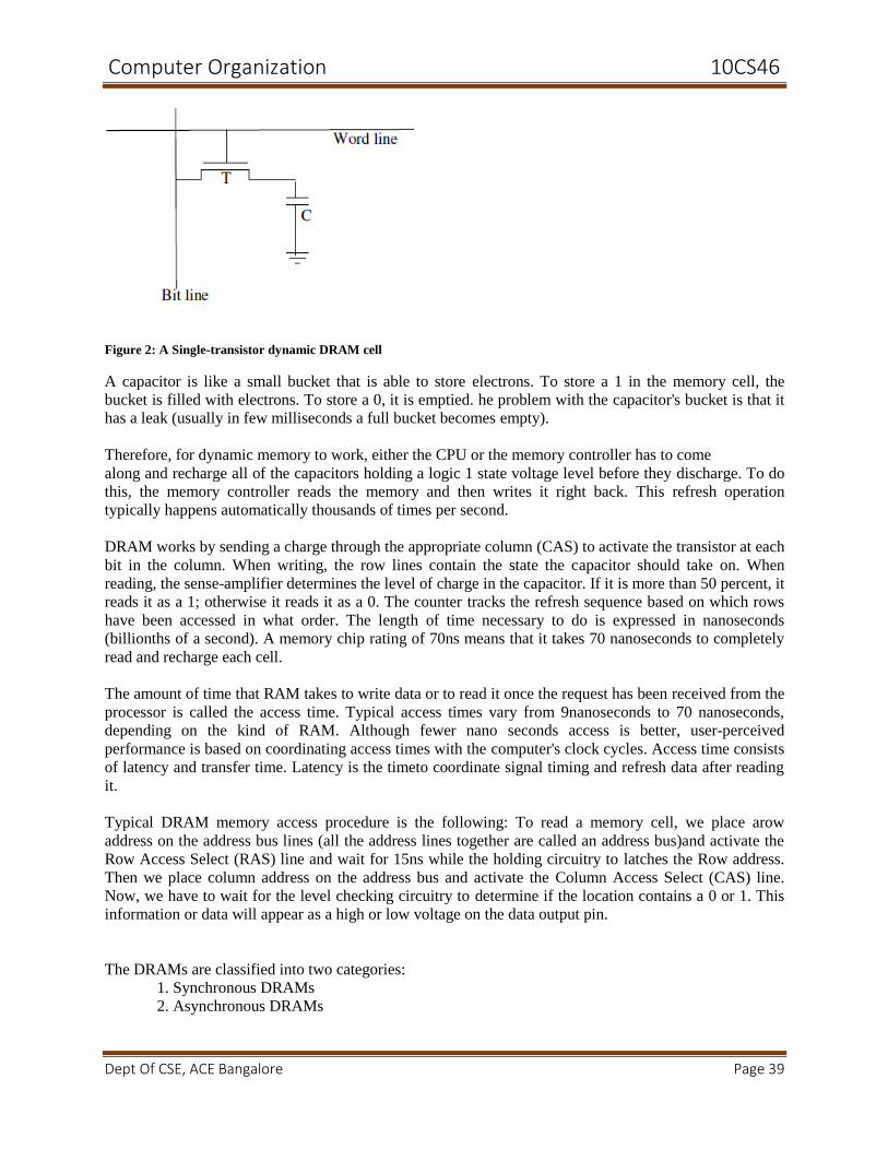
Dynamic random access memory (DRAM) is the most commonly used computer memory type. In
DRAM a transistor and a capacitor are paired to create a memory cell. Each memory cell represents a
single bit of data. The capacitor holds the bit of information (a 0 or a 1) as the voltage to charged to it.
The transistor acts as a switch that lets the control circuitry on the memory chip read the capacitor or
change its state.
Computer Organization 10CS46
Dept Of CSE, ACE Bangalore Page 39
Figure 2: A Single-transistor dynamic DRAM cell
A capacitor is like a small bucket that is able to store electrons. To store a 1 in the memory cell, the
bucket is filled with electrons. To store a 0, it is emptied. he problem with the capacitor's bucket is that it
has a leak (usually in few milliseconds a full bucket becomes empty).
Therefore, for dynamic memory to work, either the CPU or the memory controller has to come
along and recharge all of the capacitors holding a logic 1 state voltage level before they discharge. To do
this, the memory controller reads the memory and then writes it right back. This refresh operation
typically happens automatically thousands of times per second.
DRAM works by sending a charge through the appropriate column (CAS) to activate the transistor at each
bit in the column. When writing, the row lines contain the state the capacitor should take on. When
reading, the sense-amplifier determines the level of charge in the capacitor. If it is more than 50 percent, it
reads it as a 1; otherwise it reads it as a 0. The counter tracks the refresh sequence based on which rows
have been accessed in what order. The length of time necessary to do is expressed in nanoseconds
(billionths of a second). A memory chip rating of 70ns means that it takes 70 nanoseconds to completely
read and recharge each cell.
The amount of time that RAM takes to write data or to read it once the request has been received from the
processor is called the access time. Typical access times vary from 9nanoseconds to 70 nanoseconds,
depending on the kind of RAM. Although fewer nano seconds access is better, user-perceived
performance is based on coordinating access times with the computer's clock cycles. Access time consists
of latency and transfer time. Latency is the timeto coordinate signal timing and refresh data after reading
it.
Typical DRAM memory access procedure is the following: To read a memory cell, we place arow
address on the address bus lines (all the address lines together are called an address bus)and activate the
Row Access Select (RAS) line and wait for 15ns while the holding circuitry to latches the Row address.
Then we place column address on the address bus and activate the Column Access Select (CAS) line.
Now, we have to wait for the level checking circuitry to determine if the location contains a 0 or 1. This
information or data will appear as a high or low voltage on the data output pin.
The DRAMs are classified into two categories:
1. Synchronous DRAMs
2. Asynchronous DRAMs
Computer Organization 10CS46
Dept Of CSE, ACE Bangalore Page 40
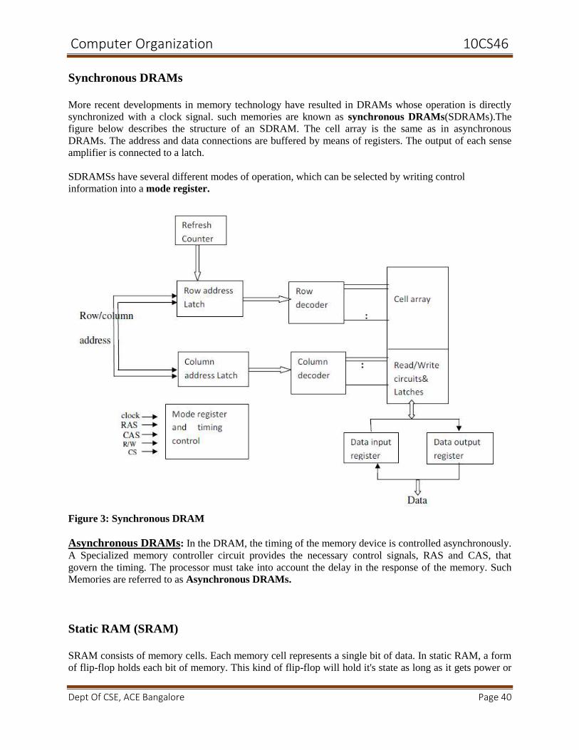
Synchronous DRAMs
More recent developments in memory technology have resulted in DRAMs whose operation is directly
synchronized with a clock signal. such memories are known as synchronous DRAMs(SDRAMs).The
figure below describes the structure of an SDRAM. The cell array is the same as in asynchronous
DRAMs. The address and data connections are buffered by means of registers. The output of each sense
amplifier is connected to a latch.
SDRAMSs have several different modes of operation, which can be selected by writing control
information into a mode register.
Figure 3: Synchronous DRAM
Asynchronous DRAMs: In the DRAM, the timing of the memory device is controlled asynchronously.
A Specialized memory controller circuit provides the necessary control signals, RAS and CAS, that
govern the timing. The processor must take into account the delay in the response of the memory. Such
Memories are referred to as Asynchronous DRAMs.
Static RAM (SRAM)
SRAM consists of memory cells. Each memory cell represents a single bit of data. In static RAM, a form
of flip-flop holds each bit of memory. This kind of flip-flop will hold it's state as long as it gets power or
Computer Organization 10CS46
Dept Of CSE, ACE Bangalore Page 41
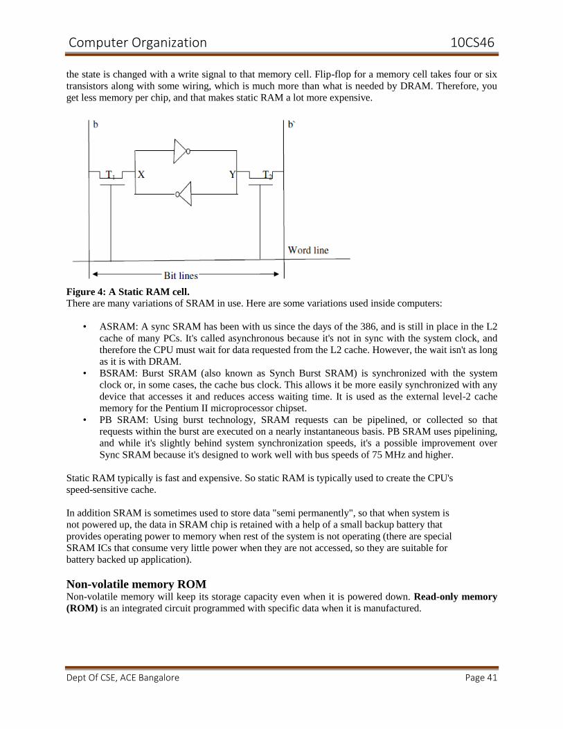
the state is changed with a write signal to that memory cell. Flip-flop for a memory cell takes four or six
transistors along with some wiring, which is much more than what is needed by DRAM. Therefore, you
get less memory per chip, and that makes static RAM a lot more expensive.
Figure 4: A Static RAM cell.
There are many variations of SRAM in use. Here are some variations used inside computers:
• ASRAM: A sync SRAM has been with us since the days of the 386, and is still in place in the L2
cache of many PCs. It's called asynchronous because it's not in sync with the system clock, and
therefore the CPU must wait for data requested from the L2 cache. However, the wait isn't as long
as it is with DRAM.
• BSRAM: Burst SRAM (also known as Synch Burst SRAM) is synchronized with the system
clock or, in some cases, the cache bus clock. This allows it be more easily synchronized with any
device that accesses it and reduces access waiting time. It is used as the external level-2 cache
memory for the Pentium II microprocessor chipset.
• PB SRAM: Using burst technology, SRAM requests can be pipelined, or collected so that
requests within the burst are executed on a nearly instantaneous basis. PB SRAM uses pipelining,
and while it's slightly behind system synchronization speeds, it's a possible improvement over
Sync SRAM because it's designed to work well with bus speeds of 75 MHz and higher.
Static RAM typically is fast and expensive. So static RAM is typically used to create the CPU's
speed-sensitive cache.
In addition SRAM is sometimes used to store data "semi permanently", so that when system is
not powered up, the data in SRAM chip is retained with a help of a small backup battery that
provides operating power to memory when rest of the system is not operating (there are special
SRAM ICs that consume very little power when they are not accessed, so they are suitable for
battery backed up application).
Non-volatile memory ROM Non-volatile memory will keep its storage capacity even when it is powered down. Read-only memory
(ROM) is an integrated circuit programmed with specific data when it is manufactured.
Computer Organization 10CS46
Dept Of CSE, ACE Bangalore Page 42
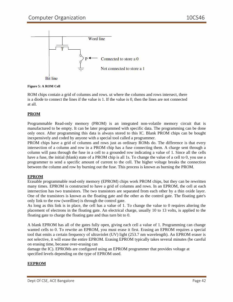
Figure 5: A ROM Cell
ROM chips contain a grid of columns and rows. ut where the columns and rows intersect, there
is a diode to connect the lines if the value is 1. If the value is 0, then the lines are not connected
at all.
PROM
Programmable Read-only memory (PROM) is an integrated non-volatile memory circuit that is
manufactured to be empty. It can be later programmed with specific data. The programming can be done
only once. After programming this data is always stored to this IC. Blank PROM chips can be bought
inexpensively and coded by anyone with a special tool called a programmer.
PROM chips have a grid of columns and rows just as ordinary ROMs do. The difference is that every
intersection of a column and row in a PROM chip has a fuse connecting them. A charge sent through a
column will pass through the fuse in a cell to a grounded row indicating a value of 1. Since all the cells
have a fuse, the initial (blank) state of a PROM chip is all 1s. To change the value of a cell to 0, you use a
programmer to send a specific amount of current to the cell. The higher voltage breaks the connection
between the column and row by burning out the fuse. This process is known as burning the PROM.
EPROM
Erasable programmable read-only memory (EPROM) chips work PROM chips, but they can be rewritten
many times. EPROM is constructed to have a grid of columns and rows. In an EPROM, the cell at each
intersection has two transistors. The two transistors are separated from each other by a thin oxide layer.
One of the transistors is known as the floating gate and the other as the control gate. The floating gate's
only link to the row (wordline) is through the control gate.
As long as this link is in place, the cell has a value of 1. To change the value to 0 requires altering the
placement of electrons in the floating gate. An electrical charge, usually 10 to 13 volts, is applied to the
floating gate to charge the floating gate and thus turn bit to 0.
A blank EPROM has all of the gates fully open, giving each cell a value of 1. Programming can change
wanted cells to 0. To rewrite an EPROM, you must erase it first. Erasing an EPROM requires a special
tool that emits a certain frequency of ultraviolet (UV) light (253.7 nm wavelength). An EPROM eraser is
not selective, it will erase the entire EPROM. Erasing EPROM typically takes several minutes (be careful
on erasing time, because over-erasing can
damage the IC). EPROMs are configured using an EPROM programmer that provides voltage at
specified levels depending on the type of EPROM used.
EEPROM
Computer Organization 10CS46
Dept Of CSE, ACE Bangalore Page 43
Electrically erasable programmable read-only memory (EEPROM) chips that can be electrically
programmed and erased. EEPROMs are typically changed 1 byte at time. Erasing EEPROM takes
typically quite long.
The drawback of EEPROM is their speed. EEPROM chips are too slow to use in many products
that make quick changes to the data stored on the chip.
Typically EEPROMs are found in electronics devices for storing the small amounts of nonvolatile
data in applications where speed is not the most important. Small EEPROMs with serial interfaces are
commonly found in many electronics devices.
Flash Flash memory is a type of EEPROM that uses in-circuit wiring to erase by applying an electrical
field to the entire chip or to predetermined sections of the chip called blocks. Flash memory works much
faster than traditional EEPROMs because it writes data in chunks, usually 512 bytes in size, instead of 1
byte at a time.
Flash memory has many applications. PC BIOS chip might be the most common form of Flash memory.
Removable solid-state storage devices are becoming increasingly popular. Smart Media and Compact
Flash cards are both well-known, especially as "electronic film" for digital cameras. Other removable
Flash memory products include Sony's Memory Stick, PCMCIA memory cards, and memory cards for
video game systems.
Speed, Size and Cost Ideally, computer memory should be fast, large and inexpensive. Unfortunately, it is impossible to meet
all the three requirements simultaneously. Increased speed and size are achieved at increased cost. Very
fast memory systems can be achieved if SRAM chips are used. These chips are expensive and for the cost
reason it is impracticable to build a large main memory using SRAM chips. The alternative used to use
DRAM chips for large main memories.
The processor fetches the code and data from the main memory to execute the program. The DRAMs
which form the main memory are slower devices. So it is necessary to insert wait states in memory
read/write cycles. This reduces the speed of execution. The solution for this problem is in the memory
system small section of SRAM is added along with the main memory, referred to as cache memory. The
program which is to be executed is loaded in the main memory, but the part of the program and data
accessed from the cache memory. The cache controller looks after this swapping between main memory
and cache memory with the help of DMA controller, Such cache memory is called secondary cache.
Recent processor have the built in cache memory called primary cache. The size of the memory is still
small compared to the demands of the large programs with the voluminous data. A solution is provided
by using secondary storage, mainly magnetic disks and magnetic tapes to implement large memory
spaces, which is available at reasonable prices.
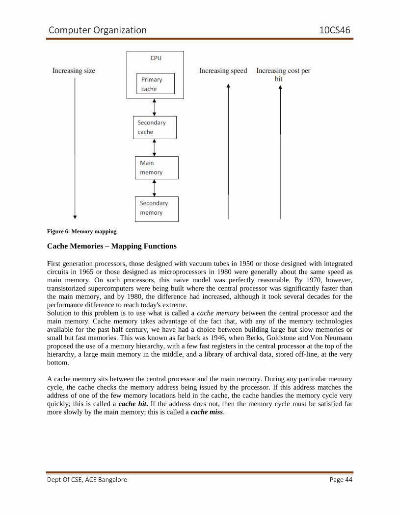
To make efficient computer system it is not possible to rely on a single memory component, but to
employ a memory hierarchy which uses all different types of memory units that gives efficient computer
system. A typical memory hierarchy is illustrated below in the figure :
Computer Organization 10CS46
Dept Of CSE, ACE Bangalore Page 44
Figure 6: Memory mapping
Cache Memories – Mapping Functions
First generation processors, those designed with vacuum tubes in 1950 or those designed with integrated
circuits in 1965 or those designed as microprocessors in 1980 were generally about the same speed as
main memory. On such processors, this naive model was perfectly reasonable. By 1970, however,
transistorized supercomputers were being built where the central processor was significantly faster than
the main memory, and by 1980, the difference had increased, although it took several decades for the
performance difference to reach today's extreme.
Solution to this problem is to use what is called a cache memory between the central processor and the
main memory. Cache memory takes advantage of the fact that, with any of the memory technologies
available for the past half century, we have had a choice between building large but slow memories or
small but fast memories. This was known as far back as 1946, when Berks, Goldstone and Von Neumann
proposed the use of a memory hierarchy, with a few fast registers in the central processor at the top of the
hierarchy, a large main memory in the middle, and a library of archival data, stored off-line, at the very
bottom.
A cache memory sits between the central processor and the main memory. During any particular memory
cycle, the cache checks the memory address being issued by the processor. If this address matches the
address of one of the few memory locations held in the cache, the cache handles the memory cycle very
quickly; this is called a cache hit. If the address does not, then the memory cycle must be satisfied far
more slowly by the main memory; this is called a cache miss.
Computer Organization 10CS46
Dept Of CSE, ACE Bangalore Page 45
Figure 7:Adding a cache to the naive view
The correspondence between the main memory and cache is specified by a Mapping function.
When the cache is full and a memory word that is not in the cache is referenced, the cache control
hardware must decide which block should be removed to create space for the new block that constitutes
the Replacement algorithm.
Mapping Functions There are three main mapping techniques which decides the cache organization:
1. Direct-mapping technique
2. Associative mapping Technique
3. Set associative mapping technique
To discuss possible methods for specifying where memory blocks are placed in the cache, we use a
specific small example, a cache consisting of 128 blocks of 16 word each, for a total of2048(2k) word,
and assuming that the main memory is addressable by a 16-bit address. The main memory has 64k word,
which will be viewed as 4K blocks of 16 word each, the consecutive addresses refer to consecutive word.
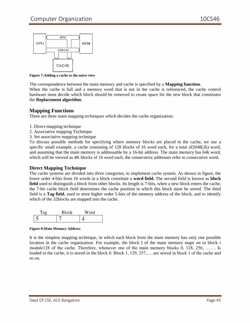
Direct Mapping Technique The cache systems are divided into three categories, to implement cache system. As shown in figure, the
lower order 4-bits from 16 words in a block constitute a word field. The second field is known as block
field used to distinguish a block from other blocks. Its length is 7-bits, when a new block enters the cache,
the 7-bit cache block field determines the cache position in which this block must be stored. The third
field is a Tag field, used to store higher order 5-bits of the memory address of the block, and to identify
which of the 32blocks are mapped into the cache.
Figure 8:Main Memory Address
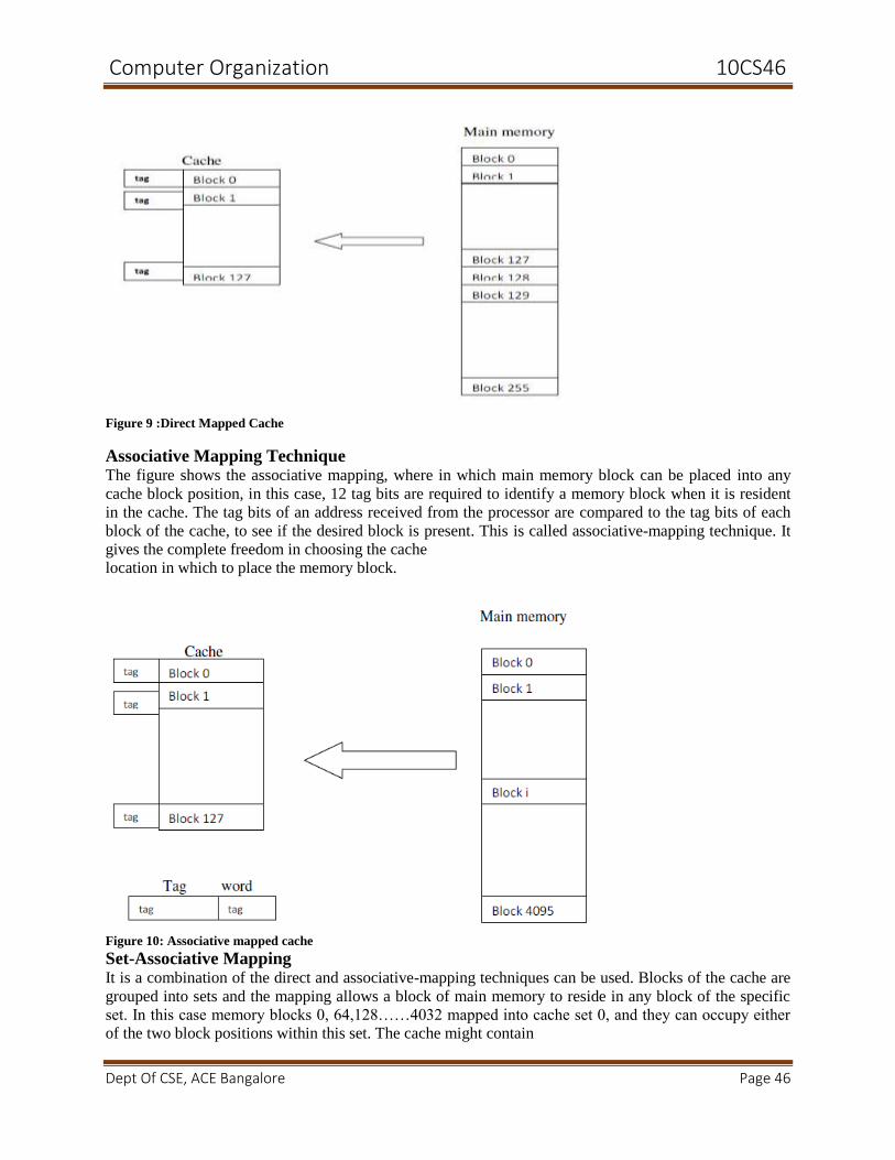
It is the simplest mapping technique, in which each block from the main memory has only one possible
location in the cache organization. For example, the block I of the main memory maps on to block i
module128 of the cache. Therefore, whenever one of the main memory blocks 0, 128, 256, ……. Is
loaded in the cache, it is stored in the block 0. Block 1, 129, 257,…..are stored in block 1 of the cache and
so on.
Computer Organization 10CS46
Dept Of CSE, ACE Bangalore Page 46
Figure 9 :Direct Mapped Cache
Associative Mapping Technique The figure shows the associative mapping, where in which main memory block can be placed into any
cache block position, in this case, 12 tag bits are required to identify a memory block when it is resident
in the cache. The tag bits of an address received from the processor are compared to the tag bits of each
block of the cache, to see if the desired block is present. This is called associative-mapping technique. It
gives the complete freedom in choosing the cache
location in which to place the memory block.
Figure 10: Associative mapped cache
Set-Associative Mapping It is a combination of the direct and associative-mapping techniques can be used. Blocks of the cache are
grouped into sets and the mapping allows a block of main memory to reside in any block of the specific
set. In this case memory blocks 0, 64,128……4032 mapped into cache set 0, and they can occupy either
of the two block positions within this set. The cache might contain
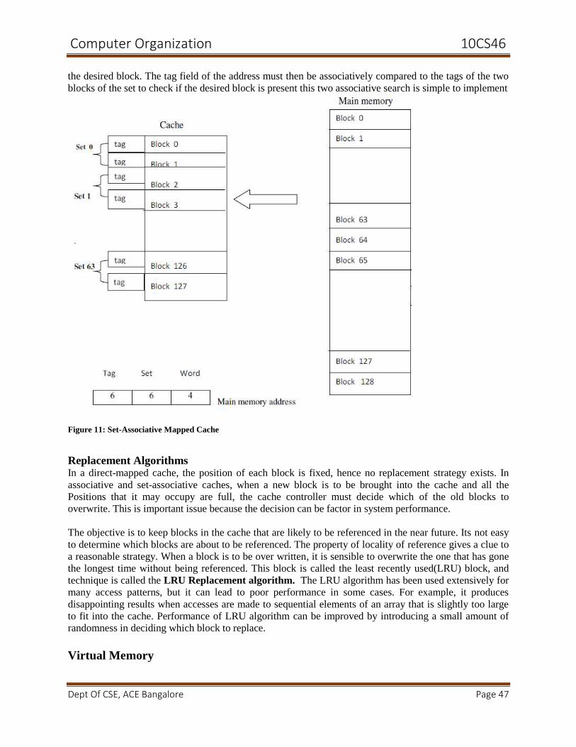
Computer Organization 10CS46
Dept Of CSE, ACE Bangalore Page 47
the desired block. The tag field of the address must then be associatively compared to the tags of the two
blocks of the set to check if the desired block is present this two associative search is simple to implement
Figure 11: Set-Associative Mapped Cache
Replacement Algorithms In a direct-mapped cache, the position of each block is fixed, hence no replacement strategy exists. In
associative and set-associative caches, when a new block is to be brought into the cache and all the
Positions that it may occupy are full, the cache controller must decide which of the old blocks to
overwrite. This is important issue because the decision can be factor in system performance.
The objective is to keep blocks in the cache that are likely to be referenced in the near future. Its not easy
to determine which blocks are about to be referenced. The property of locality of reference gives a clue to
a reasonable strategy. When a block is to be over written, it is sensible to overwrite the one that has gone
the longest time without being referenced. This block is called the least recently used(LRU) block, and
technique is called the LRU Replacement algorithm. The LRU algorithm has been used extensively for
many access patterns, but it can lead to poor performance in some cases. For example, it produces
disappointing results when accesses are made to sequential elements of an array that is slightly too large
to fit into the cache. Performance of LRU algorithm can be improved by introducing a small amount of
randomness in deciding which block to replace.
Virtual Memory
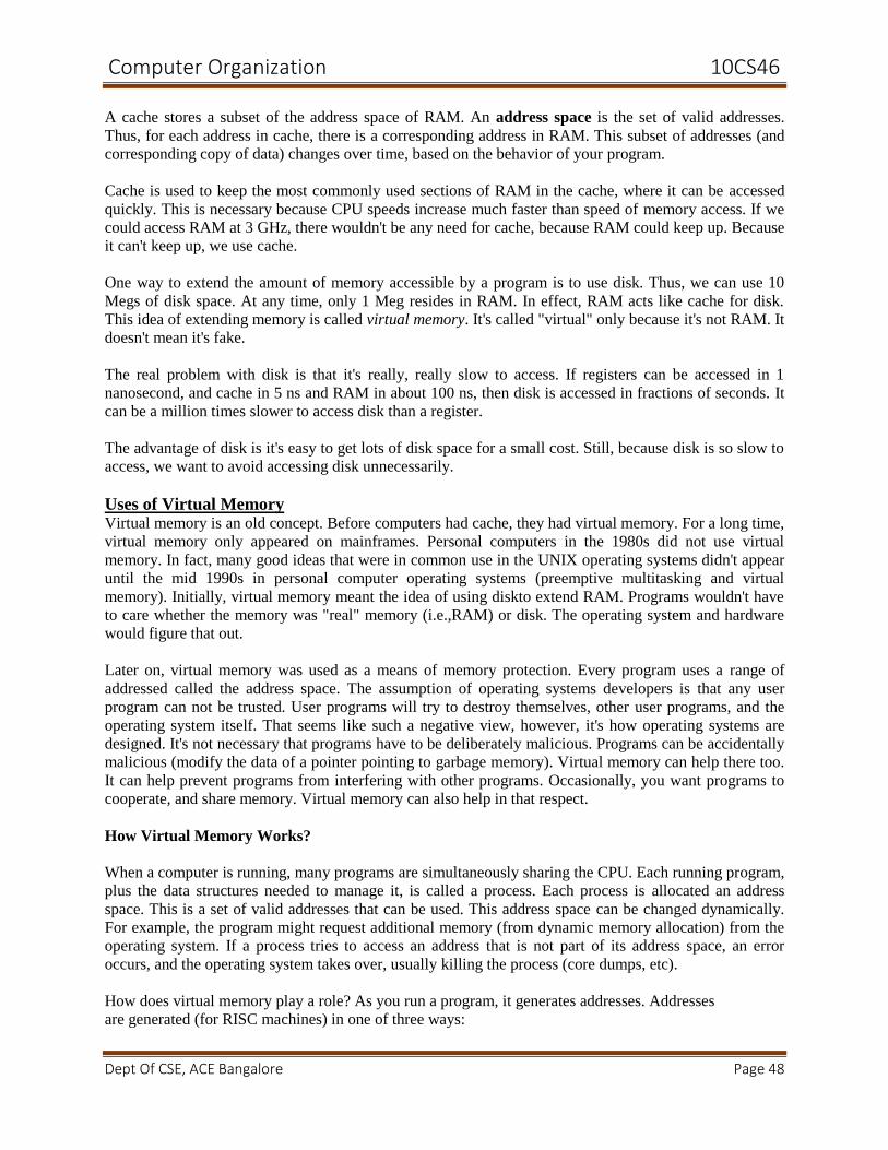
Computer Organization 10CS46
Dept Of CSE, ACE Bangalore Page 48
A cache stores a subset of the address space of RAM. An address space is the set of valid addresses.
Thus, for each address in cache, there is a corresponding address in RAM. This subset of addresses (and
corresponding copy of data) changes over time, based on the behavior of your program.
Cache is used to keep the most commonly used sections of RAM in the cache, where it can be accessed
quickly. This is necessary because CPU speeds increase much faster than speed of memory access. If we
could access RAM at 3 GHz, there wouldn't be any need for cache, because RAM could keep up. Because
it can't keep up, we use cache.
One way to extend the amount of memory accessible by a program is to use disk. Thus, we can use 10
Megs of disk space. At any time, only 1 Meg resides in RAM. In effect, RAM acts like cache for disk.
This idea of extending memory is called virtual memory. It's called "virtual" only because it's not RAM. It
doesn't mean it's fake.
The real problem with disk is that it's really, really slow to access. If registers can be accessed in 1
nanosecond, and cache in 5 ns and RAM in about 100 ns, then disk is accessed in fractions of seconds. It
can be a million times slower to access disk than a register.
The advantage of disk is it's easy to get lots of disk space for a small cost. Still, because disk is so slow to
access, we want to avoid accessing disk unnecessarily.
Uses of Virtual Memory Virtual memory is an old concept. Before computers had cache, they had virtual memory. For a long time,
virtual memory only appeared on mainframes. Personal computers in the 1980s did not use virtual
memory. In fact, many good ideas that were in common use in the UNIX operating systems didn't appear
until the mid 1990s in personal computer operating systems (preemptive multitasking and virtual
memory). Initially, virtual memory meant the idea of using diskto extend RAM. Programs wouldn't have
to care whether the memory was "real" memory (i.e.,RAM) or disk. The operating system and hardware
would figure that out.
Later on, virtual memory was used as a means of memory protection. Every program uses a range of
addressed called the address space. The assumption of operating systems developers is that any user
program can not be trusted. User programs will try to destroy themselves, other user programs, and the
operating system itself. That seems like such a negative view, however, it's how operating systems are
designed. It's not necessary that programs have to be deliberately malicious. Programs can be accidentally
malicious (modify the data of a pointer pointing to garbage memory). Virtual memory can help there too.
It can help prevent programs from interfering with other programs. Occasionally, you want programs to
cooperate, and share memory. Virtual memory can also help in that respect.
How Virtual Memory Works?
When a computer is running, many programs are simultaneously sharing the CPU. Each running program,
plus the data structures needed to manage it, is called a process. Each process is allocated an address
space. This is a set of valid addresses that can be used. This address space can be changed dynamically.
For example, the program might request additional memory (from dynamic memory allocation) from the
operating system. If a process tries to access an address that is not part of its address space, an error
occurs, and the operating system takes over, usually killing the process (core dumps, etc).
How does virtual memory play a role? As you run a program, it generates addresses. Addresses
are generated (for RISC machines) in one of three ways:
Computer Organization 10CS46
Dept Of CSE, ACE Bangalore Page 49
• A load instruction
• A store instruction
• Fetching an instruction
Load/store create data addresses, while fetching an instruction creates instruction addresses. Of course,
RAM doesn't distinguish between the two kinds of addresses. It just sees it as an address.
Each address generated by a program is considered virtual. It must be translated to a real physical address.
Thus, address translation is occurring all the time. As you might imagine, this must be handled in
hardware, if it's to be done efficiently.
You might think translating each address from virtual to physical is a crazy idea, because of how slow it
is. However, you get memory protection from address translation, so it's worth the hardware needed to get
memory protection.
Secondary Storage
Electronic data is a sequence of bits. This data can either reside in
• primary storage - main memory (RAM), relatively small, fast access, expensive (cost per MB), volatile
(go away when power goes off)
• secondary storage - disks, tape, large amounts of data, slower access, cheap (cost per MB), persistent
(remain even when power is off)
We will focus on secondary storage since the collections of data in databases are usually both too large to
fit in primary storage and must be persistent.
Hard Disks Features
• spinning platter of special material
• mechanical arm with read/write head must be close to the platter to read/write data
• data is stored magnetically (if you'd like to keep your data it is usually best to avoid using
powerful magnets near your hard disk)
• sometimes the mechanical arm digs into platter, resulting in a very bad crash and subsequent
loss of data on part of your hard disk
• storage capacity is commonly between 2GB - 11GB
• disks are random access meaning data can be read/written anywhere on the disk • to read a piece
of data, the mechanical arm must be repositioned over the place in the platter where that data is
stored, this is called the disk seek. 8 to 15 milliseconds is a common seek time.
• once the arm has been positioned the data transfer rate varies, but commonly is between 1MB
and 10MB a second
• a 5GB hard disk will cost anywhere from $300 to $1500, there are many options and vendors
• SCSI (Small Computer System Interface), special hardware to improve throughput, 100s MB
per second transfer rates
• solid state hard disks, with no mechanical parts, are starting to become commercially available,
they are generally faster and more expensive
Computer Organization 10CS46
Dept Of CSE, ACE Bangalore Page 50
Diskette or Floppy Disk • spinning platter of special material
• information stored by magnetically
• read/write head positioned by mechanical arm
• storage capacity is at a few MBs
• random access
• seek time from 10 to 40 milliseconds
• easily portable
Removable Hard Disk • like hard disk; designed to permit disk and/or disk drive to be removed and slotted into
another machine within seconds.
• more expensive than hard disk
• less reliable
Optical Disks • CD-ROM - read only (books, software releases)
• WORM - write once, read many (archival storage)
• laser encoding, not magnetic
• 30-50 ms seek times
• 640MB - 17GB storage capacity
• cheaper than hard disks per MB of storage capacity, but slower
• portable
• Jukeboxes of optical disks are becoming popular for storing really, really large collections of
data. The Mercury-20 jukebox (no I'm not selling these, just using it as atypical example)
provides access to up to 150 CD-ROMs, or in other words 94GBs of storage capacity. The
Mercury jukebox takes a maximum of four seconds to exchange and load a disc into a drive, 2.5
seconds to spin up and access the data and 10 seconds to transfer a 6.0 MB file to the computer or
server


![Cse IV Computer Organization [10cs46] Notes](https://img.pdfslide.net/doc/110x75/55cf8de4550346703b8c67e2/cse-iv-computer-organization-10cs46-notes-5640c45cf3b3d.jpg)

![Cse IV Computer Organization [10cs46] Solution](https://img.pdfslide.net/doc/110x75/55cf9d53550346d033ad2210/cse-iv-computer-organization-10cs46-solution.jpg)


