Embed Size (px)
Citation preview
SOLUTIONS MANUAL
Computer Systems Organizationand Architecture
John D. Carpinelli
Copyright © 2001, Addison Wesley Longman - All Rights Reserved
Computer Systems Organization and Architecture - Solutions Manual
Copyright 2001 Addison Wesley - All Rights Reserved Page ii
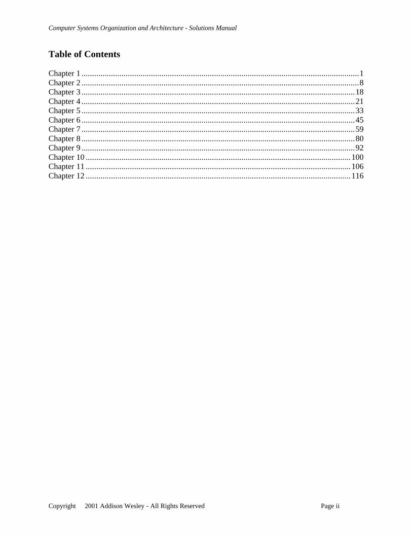
Table of Contents
Chapter 1 ....................................................................................................................................1Chapter 2 ....................................................................................................................................8Chapter 3 ..................................................................................................................................18Chapter 4 ..................................................................................................................................21Chapter 5 ..................................................................................................................................33Chapter 6 ..................................................................................................................................45Chapter 7 ..................................................................................................................................59Chapter 8 ..................................................................................................................................80Chapter 9 ..................................................................................................................................92Chapter 10 ..............................................................................................................................100Chapter 11 ..............................................................................................................................106Chapter 12 ..............................................................................................................................116
Computer Systems Organization and Architecture - Solutions Manual
Copyright 2001 Addison Wesley - All Rights Reserved Page 1
Chapter 1
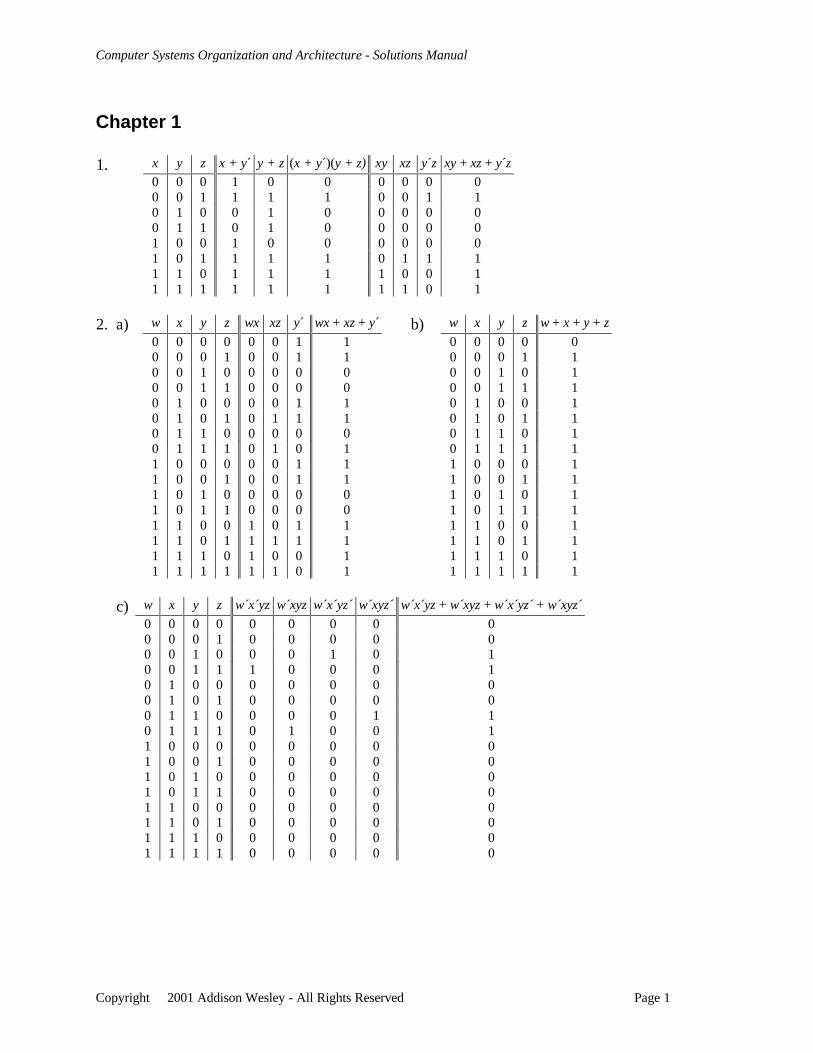
1. x y z x + y´ y + z (x + y´)(y + z) xy xz y´z xy + xz + y´z
0 0 0 1 0 0 0 0 0 00 0 1 1 1 1 0 0 1 10 1 0 0 1 0 0 0 0 00 1 1 0 1 0 0 0 0 01 0 0 1 0 0 0 0 0 01 0 1 1 1 1 0 1 1 11 1 0 1 1 1 1 0 0 11 1 1 1 1 1 1 1 0 1
2. a) w x y z wx xz y´ wx + xz + y´ b) w x y z w + x + y + z
0 0 0 0 0 0 1 1 0 0 0 0 00 0 0 1 0 0 1 1 0 0 0 1 10 0 1 0 0 0 0 0 0 0 1 0 10 0 1 1 0 0 0 0 0 0 1 1 10 1 0 0 0 0 1 1 0 1 0 0 10 1 0 1 0 1 1 1 0 1 0 1 10 1 1 0 0 0 0 0 0 1 1 0 10 1 1 1 0 1 0 1 0 1 1 1 11 0 0 0 0 0 1 1 1 0 0 0 11 0 0 1 0 0 1 1 1 0 0 1 11 0 1 0 0 0 0 0 1 0 1 0 11 0 1 1 0 0 0 0 1 0 1 1 11 1 0 0 1 0 1 1 1 1 0 0 11 1 0 1 1 1 1 1 1 1 0 1 11 1 1 0 1 0 0 1 1 1 1 0 11 1 1 1 1 1 0 1 1 1 1 1 1
c) w x y z w´x´yz w´xyz w´x´yz´ w´xyz´ w´x´yz + w´xyz + w´x´yz´ + w´xyz´
0 0 0 0 0 0 0 0 00 0 0 1 0 0 0 0 00 0 1 0 0 0 1 0 10 0 1 1 1 0 0 0 10 1 0 0 0 0 0 0 00 1 0 1 0 0 0 0 00 1 1 0 0 0 0 1 10 1 1 1 0 1 0 0 11 0 0 0 0 0 0 0 01 0 0 1 0 0 0 0 01 0 1 0 0 0 0 0 01 0 1 1 0 0 0 0 01 1 0 0 0 0 0 0 01 1 0 1 0 0 0 0 01 1 1 0 0 0 0 0 01 1 1 1 0 0 0 0 0
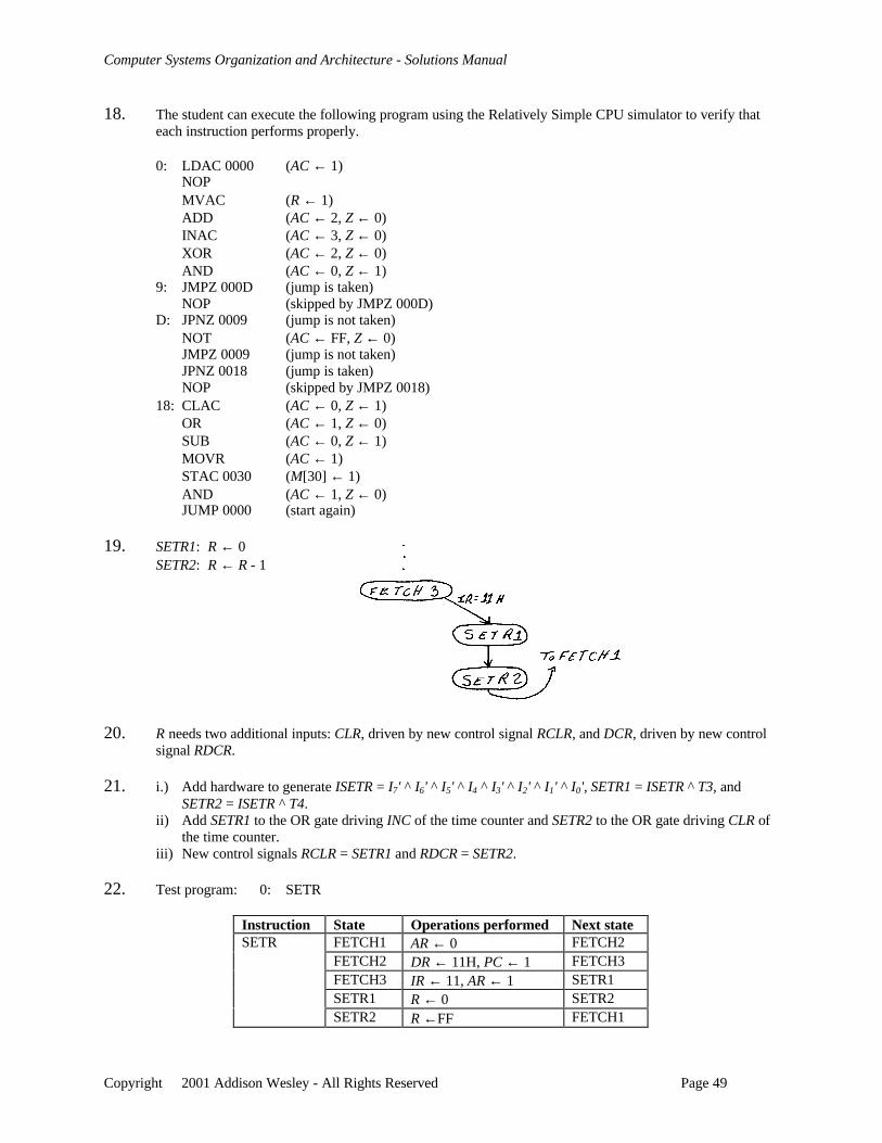
Computer Systems Organization and Architecture - Solutions Manual
Copyright 2001 Addison Wesley - All Rights Reserved Page 2
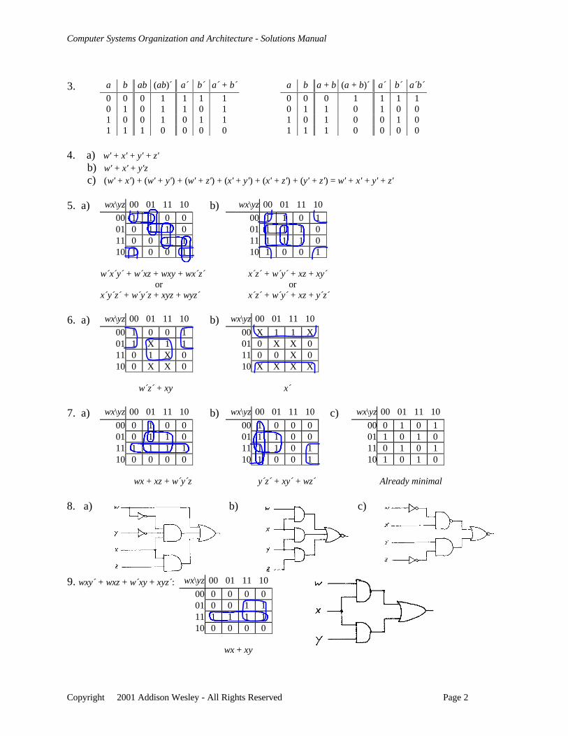
3. a b ab (ab)´ a´ b´ a´ + b´ a b a + b (a + b)´ a´ b´ a´b´
0 0 0 1 1 1 1 0 0 0 1 1 1 10 1 0 1 1 0 1 0 1 1 0 1 0 01 0 0 1 0 1 1 1 0 1 0 0 1 01 1 1 0 0 0 0 1 1 1 0 0 0 0
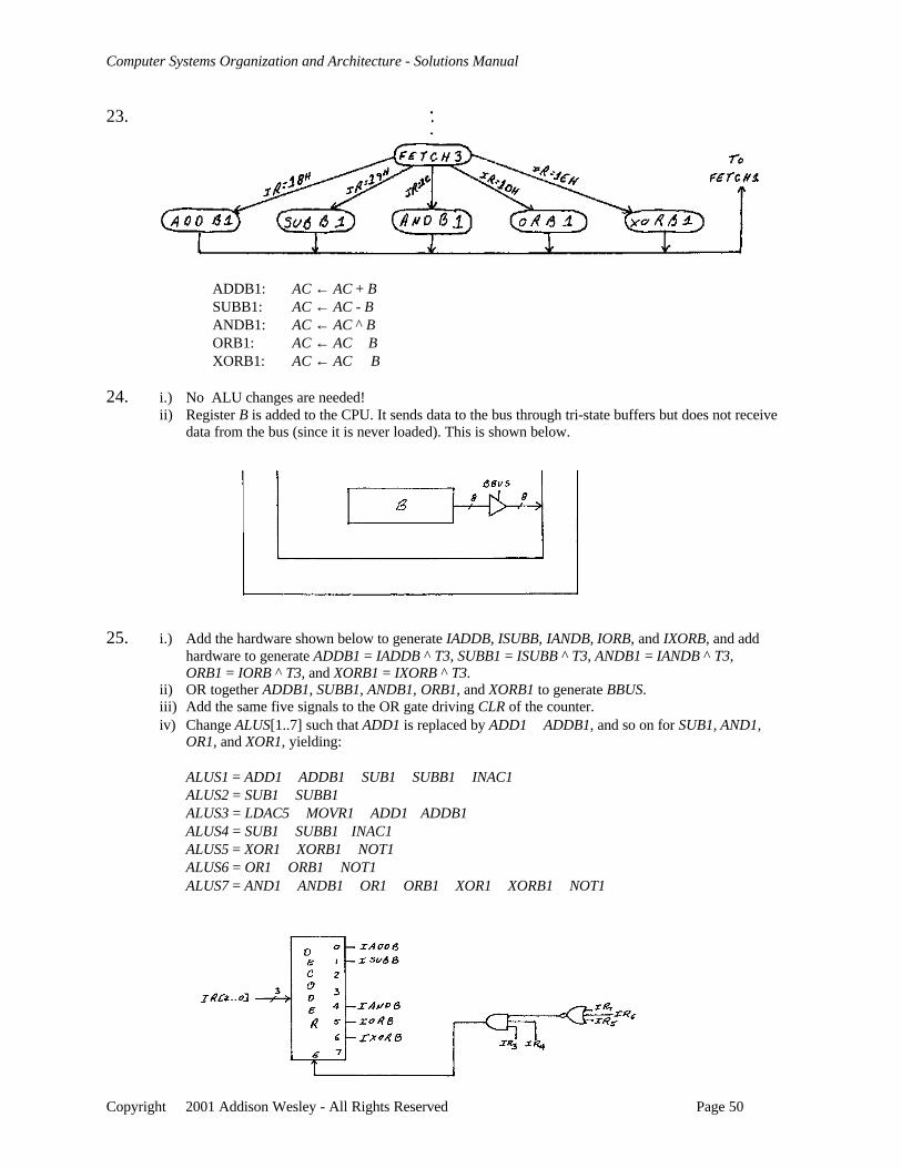
4. a) w' + x' + y' + z'b) w' + x' + y'zc) (w' + x') + (w' + y') + (w' + z') + (x' + y') + (x' + z') + (y' + z') = w' + x' + y' + z'
5. a) wx\yz 00 01 11 10 b) wx\yz 00 01 11 10
00 1 1 0 0 00 1 1 0 101 0 1 1 0 01 1 1 1 011 0 0 1 1 11 1 1 1 010 1 0 0 1 10 1 0 0 1
w´x´y´ + w´xz + wxy + wx´z´ x´z´ + w´y´ + xz + xy´ or or
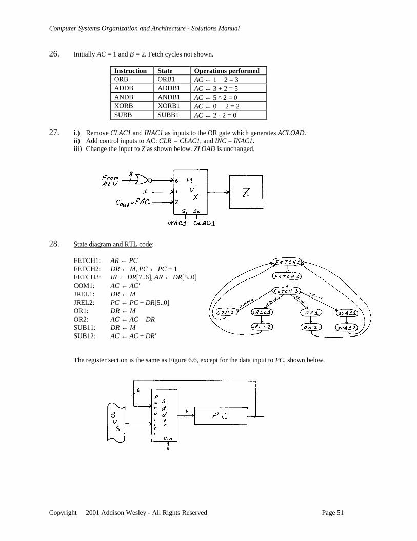
x´y´z´ + w´y´z + xyz + wyz´ x´z´ + w´y´ + xz + y´z´
6. a) wx\yz 00 01 11 10 b) wx\yz 00 01 11 10
00 1 0 0 1 00 X 1 1 X01 1 X 1 1 01 0 X X 011 0 1 X 0 11 0 0 X 010 0 X X 0 10 X X X X
w´z´ + xy x´
7. a) wx\yz 00 01 11 10 b) wx\yz 00 01 11 10 c) wx\yz 00 01 11 10
00 0 1 0 0 00 1 0 0 0 00 0 1 0 101 0 1 1 0 01 1 1 0 0 01 1 0 1 011 1 1 1 1 11 1 1 0 1 11 0 1 0 110 0 0 0 0 10 1 0 0 1 10 1 0 1 0
wx + xz + w´y´z y´z´ + xy´ + wz´ Already minimal
8. a) b) c)
9. wxy´ + wxz + w´xy + xyz´: wx\yz 00 01 11 10
00 0 0 0 001 0 0 1 111 1 1 1 110 0 0 0 0
wx + xy
Computer Systems Organization and Architecture - Solutions Manual
Copyright 2001 Addison Wesley - All Rights Reserved Page 3
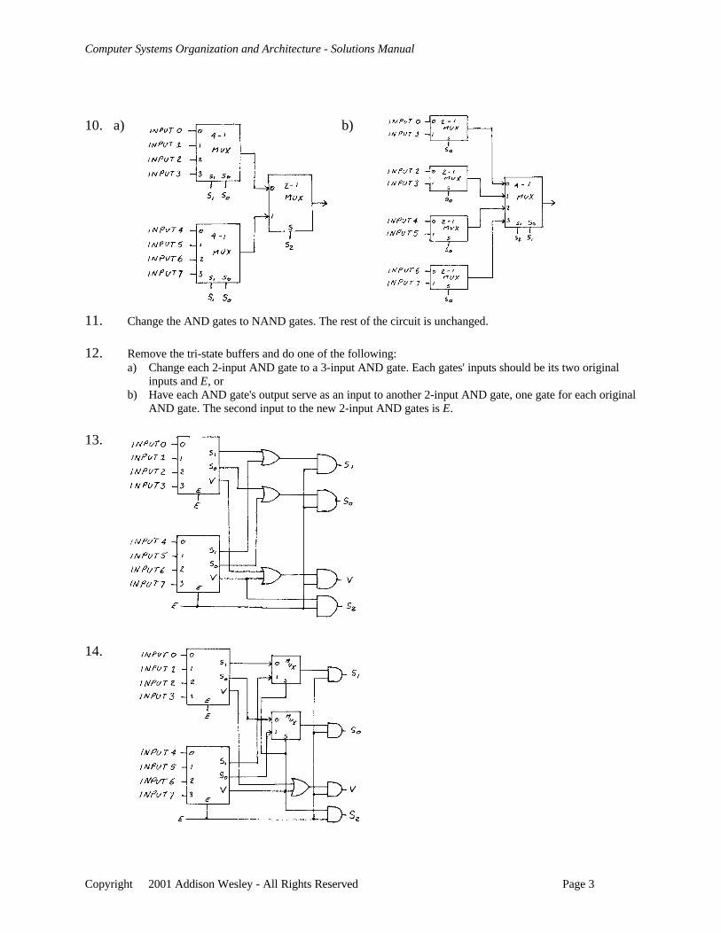
10. a) b)
11. Change the AND gates to NAND gates. The rest of the circuit is unchanged.
12. Remove the tri-state buffers and do one of the following:a) Change each 2-input AND gate to a 3-input AND gate. Each gates' inputs should be its two original
inputs and E, orb) Have each AND gate's output serve as an input to another 2-input AND gate, one gate for each original
AND gate. The second input to the new 2-input AND gates is E.
13.
14.
Computer Systems Organization and Architecture - Solutions Manual
Copyright 2001 Addison Wesley - All Rights Reserved Page 4
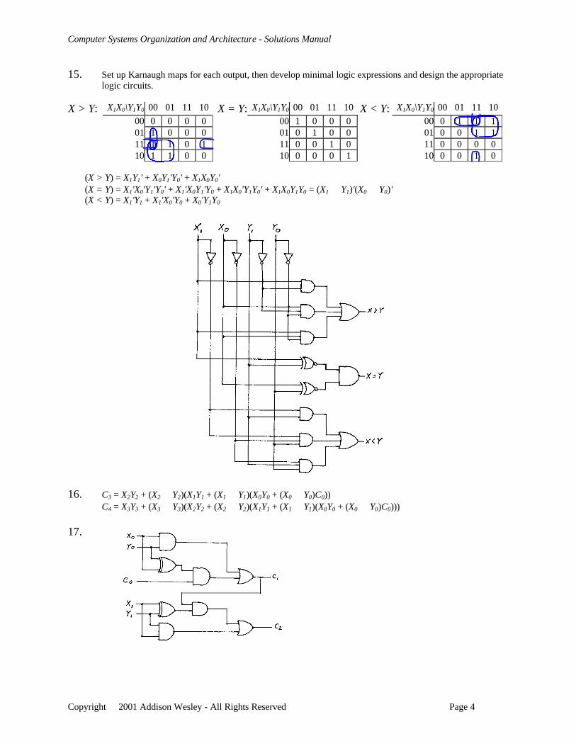
15. Set up Karnaugh maps for each output, then develop minimal logic expressions and design the appropriatelogic circuits.
X > Y: X1X0\Y1Y0 00 01 11 10 X = Y: X1X0\Y1Y0 00 01 11 10 X < Y: X1X0\Y1Y0 00 01 11 10
00 0 0 0 0 00 1 0 0 0 00 0 1 1 101 1 0 0 0 01 0 1 0 0 01 0 0 1 111 1 1 0 1 11 0 0 1 0 11 0 0 0 010 1 1 0 0 10 0 0 0 1 10 0 0 1 0
(X > Y) = X1Y1' + X0Y1'Y0' + X1X0Y0'(X = Y) = X1'X0'Y1'Y0' + X1'X0Y1'Y0 + X1X0'Y1Y0' + X1X0Y1Y0 = (X1 ⊕ Y1)'(X0 ⊕ Y0)'(X < Y) = X1'Y1 + X1'X0'Y0 + X0'Y1Y0
16. C3 = X2Y2 + (X2 ⊕ Y2)(X1Y1 + (X1 ⊕ Y1)(X0Y0 + (X0 ⊕ Y0)C0))C4 = X3Y3 + (X3 ⊕ Y3)(X2Y2 + (X2 ⊕ Y2)(X1Y1 + (X1 ⊕ Y1)(X0Y0 + (X0 ⊕ Y0)C0)))
17.
Computer Systems Organization and Architecture - Solutions Manual
Copyright 2001 Addison Wesley - All Rights Reserved Page 5
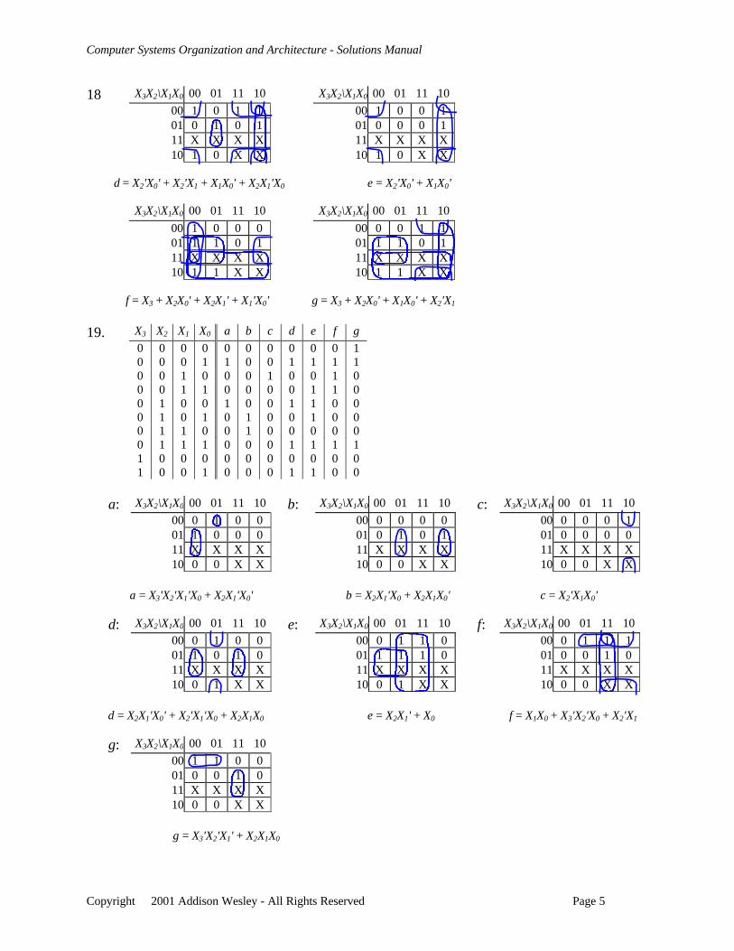
18 X3X2\X1X0 00 01 11 10 X3X2\X1X0 00 01 11 10
00 1 0 1 1 00 1 0 0 101 0 1 0 1 01 0 0 0 111 X X X X 11 X X X X10 1 0 X X 10 1 0 X X
d = X2'X0' + X2'X1 + X1X0' + X2X1'X0 e = X2'X0' + X1X0'
X3X2\X1X0 00 01 11 10 X3X2\X1X0 00 01 11 10
00 1 0 0 0 00 0 0 1 101 1 1 0 1 01 1 1 0 111 X X X X 11 X X X X10 1 1 X X 10 1 1 X X
f = X3 + X2X0' + X2X1' + X1'X0' g = X3 + X2X0' + X1X0' + X2'X1
19. X3 X2 X1 X0 a b c d e f g
0 0 0 0 0 0 0 0 0 0 10 0 0 1 1 0 0 1 1 1 10 0 1 0 0 0 1 0 0 1 00 0 1 1 0 0 0 0 1 1 00 1 0 0 1 0 0 1 1 0 00 1 0 1 0 1 0 0 1 0 00 1 1 0 0 1 0 0 0 0 00 1 1 1 0 0 0 1 1 1 11 0 0 0 0 0 0 0 0 0 01 0 0 1 0 0 0 1 1 0 0
a: X3X2\X1X0 00 01 11 10 b: X3X2\X1X0 00 01 11 10 c: X3X2\X1X0 00 01 11 10
00 0 1 0 0 00 0 0 0 0 00 0 0 0 101 1 0 0 0 01 0 1 0 1 01 0 0 0 011 X X X X 11 X X X X 11 X X X X10 0 0 X X 10 0 0 X X 10 0 0 X X
a = X3'X2'X1'X0 + X2X1'X0' b = X2X1'X0 + X2X1X0' c = X2'X1X0'
d: X3X2\X1X0 00 01 11 10 e: X3X2\X1X0 00 01 11 10 f: X3X2\X1X0 00 01 11 10
00 0 1 0 0 00 0 1 1 0 00 0 1 1 101 1 0 1 0 01 1 1 1 0 01 0 0 1 011 X X X X 11 X X X X 11 X X X X10 0 1 X X 10 0 1 X X 10 0 0 X X
d = X2X1'X0' + X2'X1'X0 + X2X1X0 e = X2X1' + X0 f = X1X0 + X3'X2'X0 + X2'X1
g: X3X2\X1X0 00 01 11 10
00 1 1 0 001 0 0 1 011 X X X X10 0 0 X X
g = X3'X2'X1' + X2X1X0
Computer Systems Organization and Architecture - Solutions Manual
Copyright 2001 Addison Wesley - All Rights Reserved Page 6
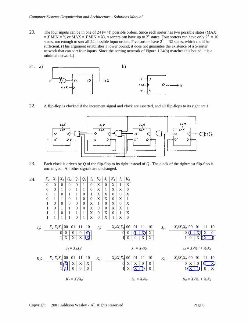
20. The four inputs can be in one of 24 (= 4!) possible orders. Since each sorter has two possible states (MAX= X MIN = Y, or MAX = Y MIN = X), n sorters can have up to 2n states. Four sorters can have only 24 = 16states, not enough to sort all 24 possible input orders. Five sorters have 25 = 32 states, which could besufficient. (This argument establishes a lower bound; it does not guarantee the existence of a 5-sorternetwork that can sort four inputs. Since the sorting network of Figure 1.24(b) matches this bound, it is aminimal network.)
21. a) b)
22. A flip-flop is clocked if the increment signal and clock are asserted, and all flip-flops to its right are 1.
23. Each clock is driven by Q of the flip-flop to its right instead of Q'. The clock of the rightmost flip-flop isunchanged. All other signals are unchanged.
24. X2 X1 X0 Q2 Q1 Q0 J2 K2 J1 K1 J0 K0
0 0 0 0 0 1 0 X 0 X 1 X0 0 1 0 1 1 0 X 1 X X 00 1 0 1 1 0 1 X X 0 0 X0 1 1 0 1 0 0 X X 0 X 11 0 0 0 0 0 X 1 0 X 0 X1 0 1 1 0 0 X 0 0 X X 11 1 0 1 1 1 X 0 X 0 1 X1 1 1 1 0 1 X 0 X 1 X 0
J2: X2\X1X0 00 01 11 10 J1: X2\X1X0 00 01 11 10 J0: X2\X1X0 00 01 11 10
0 0 0 0 1 0 0 1 X X 0 1 X X 01 X X X X 1 0 0 X X 1 0 X X 1
J2 = X1X0' J1 = X2'X0 J0 = X2'X1' + X2X1
K2: X2\X1X0 00 01 11 10 K1: X2\X1X0 00 01 11 10 K0: X2\X1X0 00 01 11 10
0 X X X X 0 X X 0 0 0 X 0 1 X1 1 0 0 0 1 X X 1 0 1 X 1 0 X
K2 = X1'X0' K1 = X2X0 K0 = X2'X1 + X2X1'
Computer Systems Organization and Architecture - Solutions Manual
Copyright 2001 Addison Wesley - All Rights Reserved Page 7
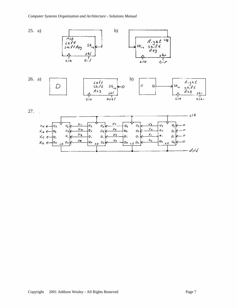
25. a) b)
26. a) b)
27.
Computer Systems Organization and Architecture - Solutions Manual
Copyright 2001 Addison Wesley - All Rights Reserved Page 8
Chapter 2
1. a) Present State D Next State
0 0 00 1 11 0 01 1 1
b) Present State T Next State
0 0 00 1 11 0 11 1 0
2. Present State S R Next State
0 0 0 00 0 1 00 1 0 10 1 1 U1 0 0 11 0 1 01 1 0 11 1 1 UU 0 0 UU 0 1 0U 1 0 1U 1 1 U
3. Add the following states to the state table. Since all additions are self-loops, it is not necessary to changethe state diagram.
Present State C I1 I0 Next State R G ASNOCAR 0 0 1 SNOCAR 1 0 0SNOCAR 0 1 0 SNOCAR 1 0 0SNOCAR 0 1 1 SNOCAR 1 0 0SPAID 1 0 1 SPAID 0 1 0SPAID 1 1 0 SPAID 0 1 0SPAID 1 1 1 SPAID 0 1 0SCHEAT 0 0 1 SCHEAT 1 0 1SCHEAT 0 1 0 SCHEAT 1 0 1SCHEAT 0 1 1 SCHEAT 1 0 1
Computer Systems Organization and Architecture - Solutions Manual
Copyright 2001 Addison Wesley - All Rights Reserved Page 9
4.
Computer Systems Organization and Architecture - Solutions Manual
Copyright 2001 Addison Wesley - All Rights Reserved Page 10
5.
6. Address Data (Mealy) Data (Moore)
0000 0000 00000001 0010 00100010 0100 01000011 0110 01100100 1000 10000101 1010 10100110 1101 11000111 1110 11101000 0000 00001001 0010 00101010 0100 01001011 0110 01101100 1000 10011101 1010 10111110 1101 11001111 1110 1110
7. Present State I Next State M
00 0 00 000 1 01 001 0 00 001 1 10 010 0 11 010 1 10 011 0 00 111 1 01 1
N1 = P1'P0I + P1P0'N0 = P1'P0'I + P1P0'I' + P1P0IM = P1P0
Computer Systems Organization and Architecture - Solutions Manual
Copyright 2001 Addison Wesley - All Rights Reserved Page 11
8.
9. Address Data (Mealy) Data (Moore)
000 000 000001 010 010010 000 000011 100 100100 111 110101 100 100110 000 001111 010 011
10. State value assignments (P3 - P0): S0 = 0000 S5 = 0001 S10 = 0010 S15 = 0011 S20 = 0100S25 = 0101 S30 = 0110 SPAID = 0111 SNOCAR = 1000 SCHEAT = 1001
N3 = C'N2 = P3'CI1I0 + P3'(P2 + P1)CI1I0' + P3'(P2 + P1P0)CI1'I0 + P2CI1'I0'N1 = P3'(P2 + P1 + P0)CI1I0 + P3'(P2 + P1')CI1I0' + P3'(P1'P0 + P1P0' + P2P1P0)CI1'I0 + P1P0CI1'I0'N0 = P3'(P2 + P1 + P0')CI1I0 + P3'(P0 + P2P1)CI1I0' + P3'(P0' + P2P1)CI1'I0 + P3'P0CI1'I0' + P3P0C
+ P3'(P2' + P1' + P0')C'R = SPAID'G = SPAID
A = SCHEAT
11. State value assignments (P3 - P0): S0 = 0000 S5 = 0001 S10 = 0010 S15 = 0011 S20 = 0100S25 = 0101 S30 = 0110 SPAID = 0111 SNOCAR = 1000 SCHEAT = 1001
N3 = C'N2 = P3'CI1I0 + P3'(P2 + P1)CI1I0' + P3'(P2 + P1P0)CI1'I0 + P2CI1'I0'N1 = P3'(P2 + P1 + P0)CI1I0 + P3'(P2 + P1')CI1I0' + P3'(P1'P0 + P1P0' + P2P1P0)CI1'I0 + P1P0CI1'I0'N0 = P3'(P2 + P1 + P0')CI1I0 + P3'(P0 + P2P1)CI1I0' + P3'(P0' + P2P1)CI1'I0 + P3'P0CI1'I0' + P3P0C
+ P3'(P2' + P1' + P0')C'R = G'G = P3'(P2 + P1)CI1I0 + P3'P2P0CI1 + P3'P2P1C(I1 + I0) + P3'P2P1P0CA = P3'(P2 + P1 + P0)C'
Computer Systems Organization and Architecture - Solutions Manual
Copyright 2001 Addison Wesley - All Rights Reserved Page 12
12. Address Data
0000XXX 1001101 1001101 1001101 1001101 0000100 0001100 0010100 01011000001XXX 1001101 1001101 1001101 1001101 0001100 0010100 0011100 01101000010XXX 1001101 1001101 1001101 1001101 0010100 0011100 0100100 01110100011XXX 1001101 1001101 1001101 1001101 0011100 0100100 0101100 01110100100XXX 1001101 1001101 1001101 1001101 0100100 0101100 0110100 01110100101XXX 1001101 1001101 1001101 1001101 0101100 0110100 0111010 01110100110XXX 1001101 1001101 1001101 1001101 0110100 0111010 0111010 01110100111XXX 1000100 1000100 1000100 1000100 0111010 0111010 0111010 01110101000XXX 1000100 1000100 1000100 1000100 0000100 0000100 0000100 00001001001XXX 1001101 1001101 1001101 1001101 0000100 0000100 0000100 00001001010XXX 1000100 1000100 1000100 1000100 1000100 1000100 1000100 10001001011XXX 1000100 1000100 1000100 1000100 1000100 1000100 1000100 10001001100XXX 1000100 1000100 1000100 1000100 1000100 1000100 1000100 10001001101XXX 1000100 1000100 1000100 1000100 1000100 1000100 1000100 10001001110XXX 1000100 1000100 1000100 1000100 1000100 1000100 1000100 10001001111XXX 1000100 1000100 1000100 1000100 1000100 1000100 1000100 1000100
13. N2: P2P1\P0U 00 01 11 10 N1: P2P1\P0U 00 01 11 10 N2: P2P1\P0U 00 01 11 10
00 0 0 0 0 00 0 0 1 0 00 0 1 0 101 0 0 1 0 01 1 1 0 1 01 0 1 0 111 0 0 0 0 11 0 0 0 0 11 0 0 0 010 1 1 0 1 10 0 0 0 0 10 0 1 0 1
14. The next state logic is the same as for the Moore machine.
N2 = P2P0' + P2U' + P1P0UN1 = P1P0' + P1U' + P2'P1'P0UN0 = P0'U + P0U'C = P2'P1'P0'U' + P2P1'P0UV2 = P2'P1P0U + P2P1'P0' + P2P1'P0U'V1 = P2'P1'P0U + P2'P1P0' + P2'P1P0U'V0 = (P2' + P1')P0'U + (P2' + P1)P0U'
15. All possible next state values are already used.
Computer Systems Organization and Architecture - Solutions Manual
Copyright 2001 Addison Wesley - All Rights Reserved Page 13
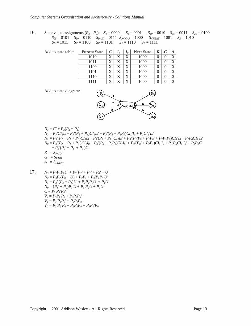
16. State value assignments (P3 - P0): S0 = 0000 S5 = 0001 S10 = 0010 S15 = 0011 S20 = 0100S25 = 0101 S30 = 0110 SPAID = 0111 SNOCAR = 1000 SCHEAT = 1001 SA = 1010SB = 1011 SC = 1100 SD = 1101 SE = 1110 SF = 1111
Add to state table: Present State C I1 I0 Next State R G A1010 X X X 1000 0 0 01011 X X X 1000 0 0 01100 X X X 1000 0 0 01101 X X X 1000 0 0 01110 X X X 1000 0 0 01111 X X X 1000 0 0 0
Add to state diagram:
N3 = C' + P3(P2 + P1)N2 = P3'CI1I0 + P3'(P2 + P1)CI1I0' + P3'(P2 + P1P0)CI1'I0 + P2CI1'I0'N1 = P3'(P2 + P1 + P0)CI1I0 + P3'(P2 + P1')CI1I0' + P3'(P1'P0 + P1P0' + P2P1P0)CI1'I0 + P1P0CI1'I0'N0 = P3'(P2 + P1 + P0')CI1I0 + P3'(P0 + P2P1)CI1I0' + P3'(P0' + P2P1)CI1'I0 + P3'P0CI1'I0' + P3P0C
+ P3'(P2' + P1' + P0')C'R = SPAID'G = SPAID
A = SCHEAT
17. N3 = P2P1P0U' + P3(P2' + P1' + P0' + U)N2 = P3P2(P0 + U) + P2P1 + P3'P1P0'U'N1 = P3' (P2 + P1)U' + P2P1P0U' + P1UN0 = (P3' + P2)P1'U + P3'P2U + P0U'C = P2'P1'P0'V2 = P3P1'P0 + P3P2P0'V1 = P3'P1P0' + P2P1P0
V0 = P3'P2'P0 + P2P1P0 + P3P1'P0
Computer Systems Organization and Architecture - Solutions Manual
Copyright 2001 Addison Wesley - All Rights Reserved Page 14
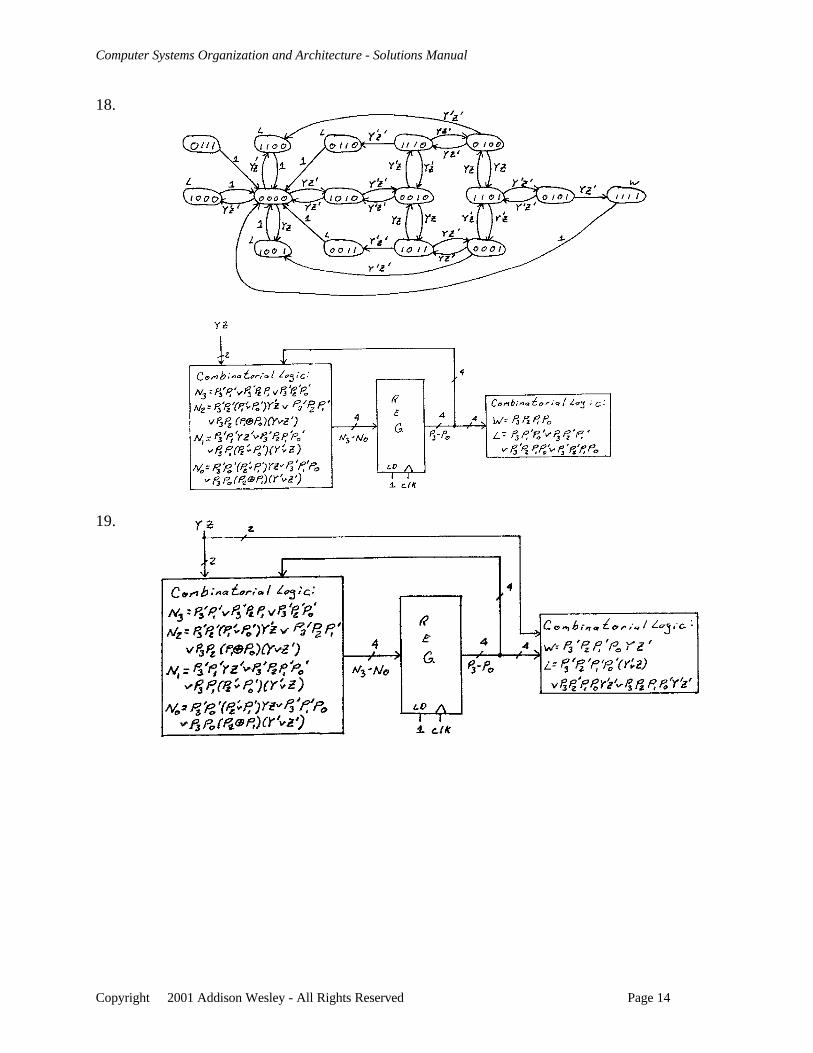
18.
19.
Computer Systems Organization and Architecture - Solutions Manual
Copyright 2001 Addison Wesley - All Rights Reserved Page 15
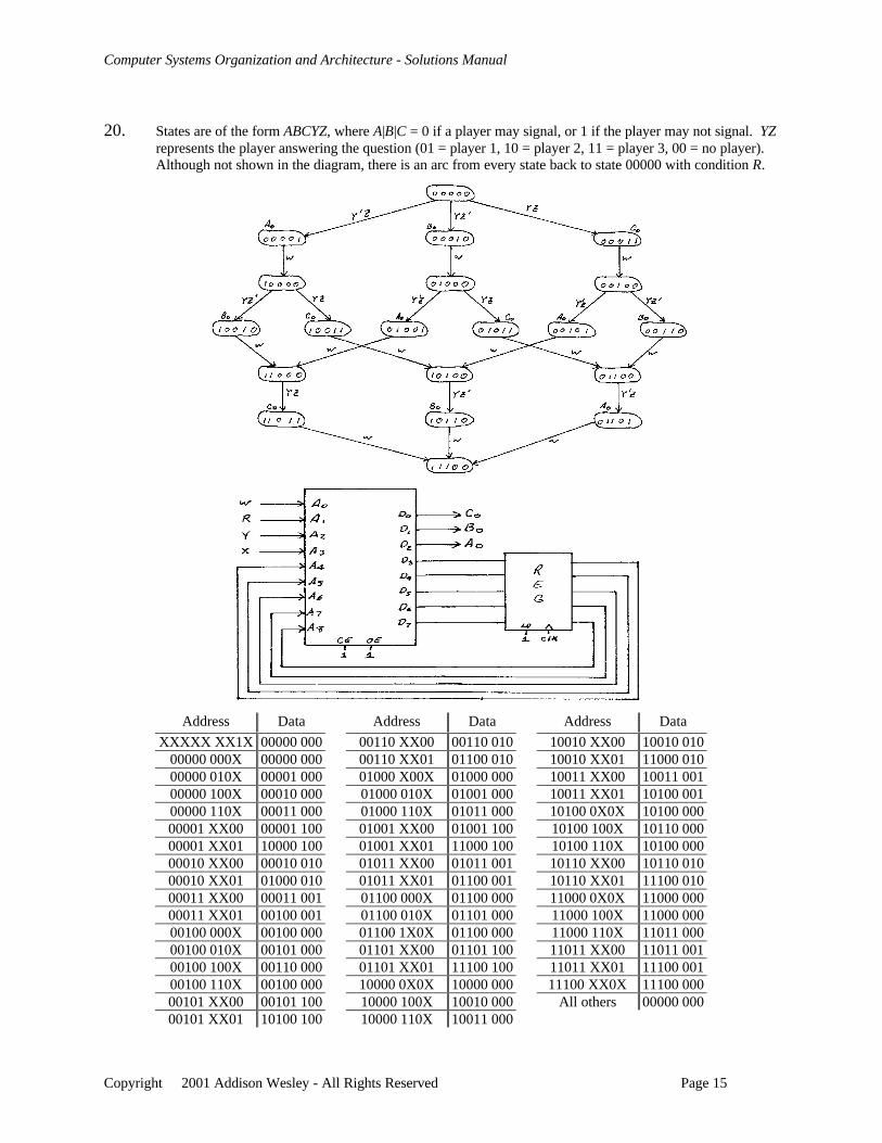
20. States are of the form ABCYZ, where A|B|C = 0 if a player may signal, or 1 if the player may not signal. YZrepresents the player answering the question (01 = player 1, 10 = player 2, 11 = player 3, 00 = no player).Although not shown in the diagram, there is an arc from every state back to state 00000 with condition R.
Address Data Address Data Address Data
XXXXX XX1X 00000 000 00110 XX00 00110 010 10010 XX00 10010 01000000 000X 00000 000 00110 XX01 01100 010 10010 XX01 11000 01000000 010X 00001 000 01000 X00X 01000 000 10011 XX00 10011 00100000 100X 00010 000 01000 010X 01001 000 10011 XX01 10100 00100000 110X 00011 000 01000 110X 01011 000 10100 0X0X 10100 00000001 XX00 00001 100 01001 XX00 01001 100 10100 100X 10110 00000001 XX01 10000 100 01001 XX01 11000 100 10100 110X 10100 00000010 XX00 00010 010 01011 XX00 01011 001 10110 XX00 10110 01000010 XX01 01000 010 01011 XX01 01100 001 10110 XX01 11100 01000011 XX00 00011 001 01100 000X 01100 000 11000 0X0X 11000 00000011 XX01 00100 001 01100 010X 01101 000 11000 100X 11000 00000100 000X 00100 000 01100 1X0X 01100 000 11000 110X 11011 00000100 010X 00101 000 01101 XX00 01101 100 11011 XX00 11011 00100100 100X 00110 000 01101 XX01 11100 100 11011 XX01 11100 00100100 110X 00100 000 10000 0X0X 10000 000 11100 XX0X 11100 00000101 XX00 00101 100 10000 100X 10010 000 All others 00000 00000101 XX01 10100 100 10000 110X 10011 000
Computer Systems Organization and Architecture - Solutions Manual
Copyright 2001 Addison Wesley - All Rights Reserved Page 16
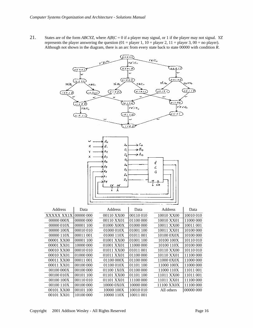
21. States are of the form ABCYZ, where A|B|C = 0 if a player may signal, or 1 if the player may not signal. YZrepresents the player answering the question (01 = player 1, 10 = player 2, 11 = player 3, 00 = no player).Although not shown in the diagram, there is an arc from every state back to state 00000 with condition R.
Address Data Address Data Address Data
XXXXX XX1X 00000 000 00110 XX00 00110 010 10010 XX00 10010 01000000 000X 00000 000 00110 XX01 01100 000 10010 XX01 11000 00000000 010X 00001 100 01000 X00X 01000 000 10011 XX00 10011 00100000 100X 00010 010 01000 010X 01001 100 10011 XX01 10100 00000000 110X 00011 001 01000 110X 01011 001 10100 0X0X 10100 00000001 XX00 00001 100 01001 XX00 01001 100 10100 100X 10110 01000001 XX01 10000 000 01001 XX01 11000 000 10100 110X 10100 00000010 XX00 00010 010 01011 XX00 01011 001 10110 XX00 10110 01000010 XX01 01000 000 01011 XX01 01100 000 10110 XX01 11100 00000011 XX00 00011 001 01100 000X 01100 000 11000 0X0X 11000 00000011 XX01 00100 000 01100 010X 01101 100 11000 100X 11000 00000100 000X 00100 000 01100 1X0X 01100 000 11000 110X 11011 00100100 010X 00101 100 01101 XX00 01101 100 11011 XX00 11011 00100100 100X 00110 010 01101 XX01 11100 000 11011 XX01 11100 00000100 110X 00100 000 10000 0X0X 10000 000 11100 XX0X 11100 00000101 XX00 00101 100 10000 100X 10010 010 All others 00000 00000101 XX01 10100 000 10000 110X 10011 001
Computer Systems Organization and Architecture - Solutions Manual
Copyright 2001 Addison Wesley - All Rights Reserved Page 17
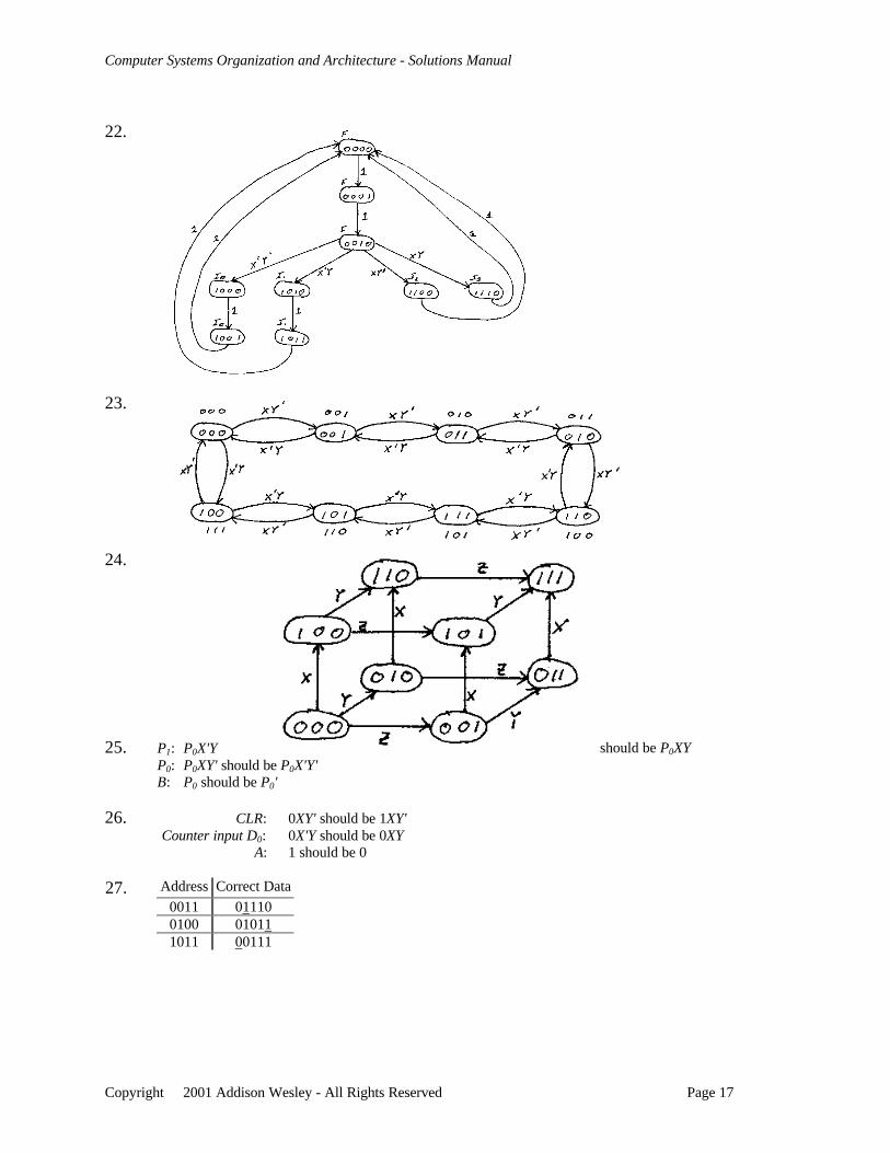
22.
23.
24.
25. P1: P0X'Y should be P0XYP0: P0XY' should be P0X'Y'B: P0 should be P0'
26. CLR: 0XY' should be 1XY' Counter input D0: 0X'Y should be 0XY
A: 1 should be 0
27. Address Correct Data
0011 011100100 010111011 00111
Computer Systems Organization and Architecture - Solutions Manual
Copyright 2001 Addison Wesley - All Rights Reserved Page 18
Chapter 3
1. a) Data movement b) Data operation c) Program control d) Data operation e) Data operation
2. a) Data operation b) Program control c) Data movement d) Data movement e) Data operation
3. a) Direct b) Implied c) Implicit
4. a) Implicit b) Direct c) Implicit
5. a) Implicit b) Direct c) Implicit
6. a) Register Direct b) Immediate c) Implicit d) Immediate e) Direct
7. a) Implicit b) Direct c) Indirect d) Register Indirect e) Register Direct
8. a) Register Direct b) Register Indirect c) Implicit d) Implicit e) Immediate
9. a) AC = 11 b) AC = 12 c) AC = 10 d) AC = 11 e) AC = 10 f) AC = 33 g) AC = 41
10. a) AC = 11 b) AC = 12 c) AC = 30 d) AC = 31 e) AC = 10 f) AC = 23 g) AC = 31
11. a) AC = 11 b) AC = 12 c) AC = 20 d) AC = 21 e) AC = 10 f) AC = 43 g) AC = 21
12. a) MUL X,B,C b) MOV X,B c) LOAD B d) PUSH AADD X,X,A MUL X,C MUL C PUSH BADD X,X,D ADD X,A ADD A PUSH C
ADD X,D ADD D MULSTORE X PUSH D
ADDADDPOP X
13. a) MUL T,A,B b) MOV T,A c) LOAD A d) PUSH AMUL T,T,C MUL T,B MUL B PUSH BADD X,E,F MUL T,C MUL C MULMUL X,X,D MOV X,E STORE T PUSH CADD X,X,T ADD X,F LOAD E MUL
MUL X,D ADD F PUSH DADD X,T MULT D PUSH E
ADD T PUSH FSTORE X ADD
MULADDPOP X
Computer Systems Organization and Architecture - Solutions Manual
Copyright 2001 Addison Wesley - All Rights Reserved Page 19
14. a) MUL X,B,C b) MOV T,B c) LOAD B d) PUSH ASUB X,A,X MUL T,C MUL C PUSH BMUL T,E,F MOV X,A STORE T PUSH CADD T,T,D SUB X,T LOAD A MULMUL X,X,T MOV T,E SUB T SUB
MUL T,F STORE X PUSH DADD T,D LOAD E PUSH EMUL X,T MUL F PUSH F
ADD D MULMUL X ADDSTORE X MUL
POP X
15. Processor Time per instruction # Instructions Total time
0 35 ns 4 140 ns1 50 ns 3 150 ns2 70 ns 2 140 ns3 100 ns 1 100 ns � fastest
16. Processor Time per instruction # Instructions Total time
0 35 ns 8 280 ns1 50 ns 5 250 ns � fastest2 70 ns 4 280 ns3 100 ns 3 300 ns
17. Processor Time per instruction # Instructions Total time
0 35 ns 12 420 ns � fastest1 50 ns 9 450 ns2 70 ns 7 490 ns3 100 ns 5 500 ns
18. Processor Time per instruction # Instructions Total time
0 35 ns 12 420 ns � fastest1 50 ns 11 550 ns2 70 ns 8 560 ns3 100 ns 5 500 ns
19. LDAC 1001HMVACLDAC 1002HADDMVACLDAC 1003HADDMVACLDAC 1004HADDMVACLDAC 1005HADDMVAC
LDAC 1006HADDMVACLDAC 1007HADDMVACLDAC 1008HADDMVACLDAC 1009HADDMVACLDAC 100AHADDSTAC 1000H
Computer Systems Organization and Architecture - Solutions Manual
Copyright 2001 Addison Wesley - All Rights Reserved Page 20
20.
Loop:
LXI H, 1001HMVI B,0AHXRA AADD MINX HDCR BJNZ LoopSTA 1000H
21.
Loop:
CLACINACSTAC FAINACSTAC FBSTAC CountSTAC FNMVACLDACSUBJMPZ DoneLDAC FAMVACLDAC FBADDSTAC FALDAC CountINACSTAC CountMVACLDAC nSUBJMPZ DoneA
FA = 1
FB = 2Count = 2FN = 2
If n = 2 then done
FA = FA + FB
Count = Count + 1
If Count = n then done, result in FA
DoneA:
DoneB:
Done:
LDAC FBMVACLDAC FAADDSTAC FBLDAC CountINACSTAC CountMVACLDAC nSUBJMPZ DoneBJUMP LoopLDAC FASTAC FNJUMP DoneLDAC FBSTAC FN…
FB = FB + FA
Count = Count + 1
If Count = n then done, result in FBNot done, loop back
FN = FA
FN = FB
22.
Loop:
Done:
LDA nMOV D,AMVI B,1MVI A,2MOV C,ADCR DDCR DJZ DoneADD BMOV B,ADCR DJZ DoneADD CMOV C,ADCR DJNZ LoopSTA FN
D = nB = FA
C = FB
Initially A = FA
FA = FA + FBIf D = 0 then done
FB = FB + FAIf D = 0 then doneNot done, loop backStore FN
Computer Systems Organization and Architecture - Solutions Manual
Copyright 2001 Addison Wesley - All Rights Reserved Page 21
Chapter 4
1.
2.
Computer Systems Organization and Architecture - Solutions Manual
Copyright 2001 Addison Wesley - All Rights Reserved Page 22
3.
4.
Computer Systems Organization and Architecture - Solutions Manual
Copyright 2001 Addison Wesley - All Rights Reserved Page 23
5.
6.
Computer Systems Organization and Architecture - Solutions Manual
Copyright 2001 Addison Wesley - All Rights Reserved Page 24
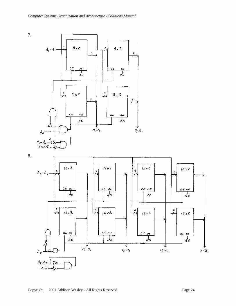
7.
8.
Computer Systems Organization and Architecture - Solutions Manual
Copyright 2001 Addison Wesley - All Rights Reserved Page 25
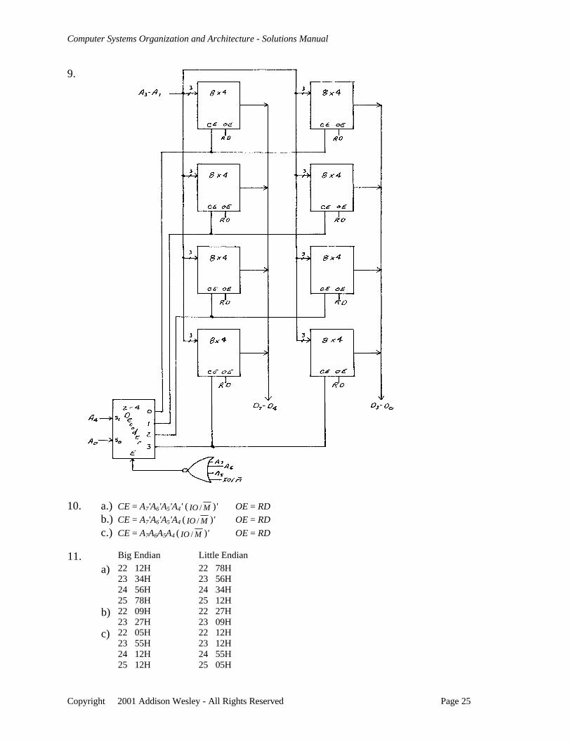
9.
10. a.) CE = A7'A6'A5'A4' ( MIO / )' OE = RD
b.) CE = A7'A6'A5'A4 ( MIO / )' OE = RD
c.) CE = A7A6A5A4 ( MIO / )' OE = RD
11. Big Endian Little Endian
a) 22 12H23 34H24 56H25 78H
22 78H23 56H24 34H25 12H
b) 22 09H23 27H
22 27H23 09H
c) 22 05H23 55H24 12H25 12H
22 12H23 12H24 55H25 05H
Computer Systems Organization and Architecture - Solutions Manual
Copyright 2001 Addison Wesley - All Rights Reserved Page 26
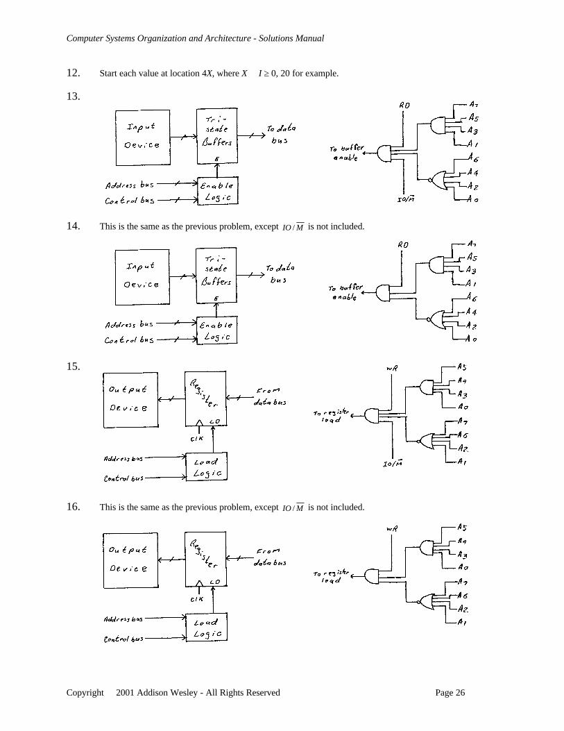
12. Start each value at location 4X, where X ∈ I ≥ 0, 20 for example.
13.
14. This is the same as the previous problem, except MIO / is not included.
15.
16. This is the same as the previous problem, except MIO / is not included.
Computer Systems Organization and Architecture - Solutions Manual
Copyright 2001 Addison Wesley - All Rights Reserved Page 27
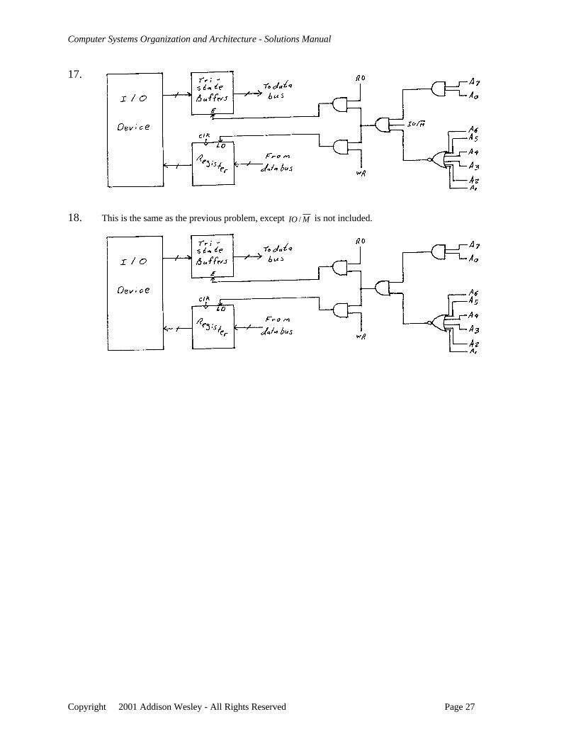
17.
18. This is the same as the previous problem, except MIO / is not included.
Computer Systems Organization and Architecture - Solutions Manual
Copyright 2001 Addison Wesley - All Rights Reserved Page 28
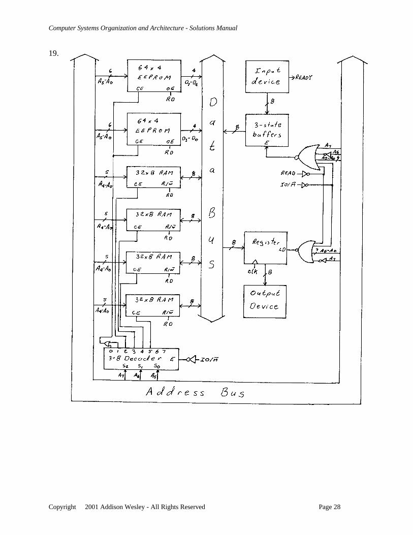
19.
Computer Systems Organization and Architecture - Solutions Manual
Copyright 2001 Addison Wesley - All Rights Reserved Page 29
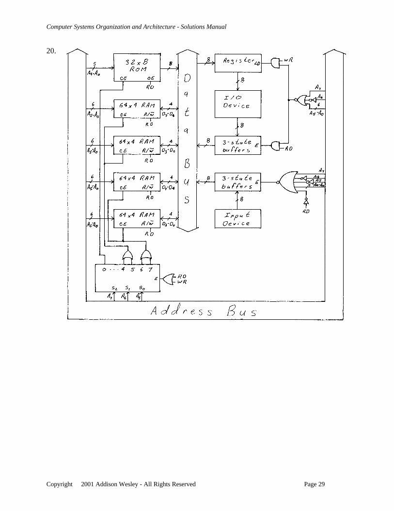
20.
Computer Systems Organization and Architecture - Solutions Manual
Copyright 2001 Addison Wesley - All Rights Reserved Page 30
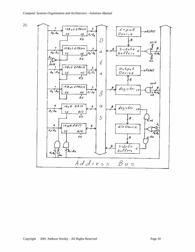
21.
Computer Systems Organization and Architecture - Solutions Manual
Copyright 2001 Addison Wesley - All Rights Reserved Page 31
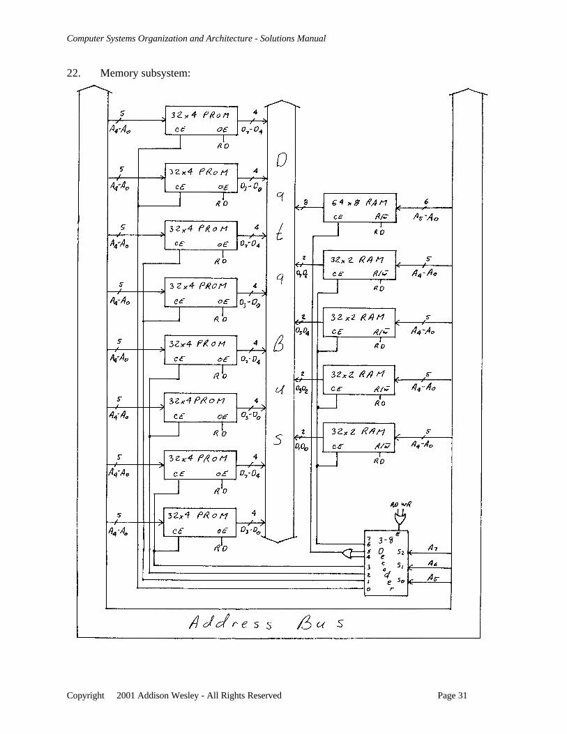
22. Memory subsystem:
Computer Systems Organization and Architecture - Solutions Manual
Copyright 2001 Addison Wesley - All Rights Reserved Page 32
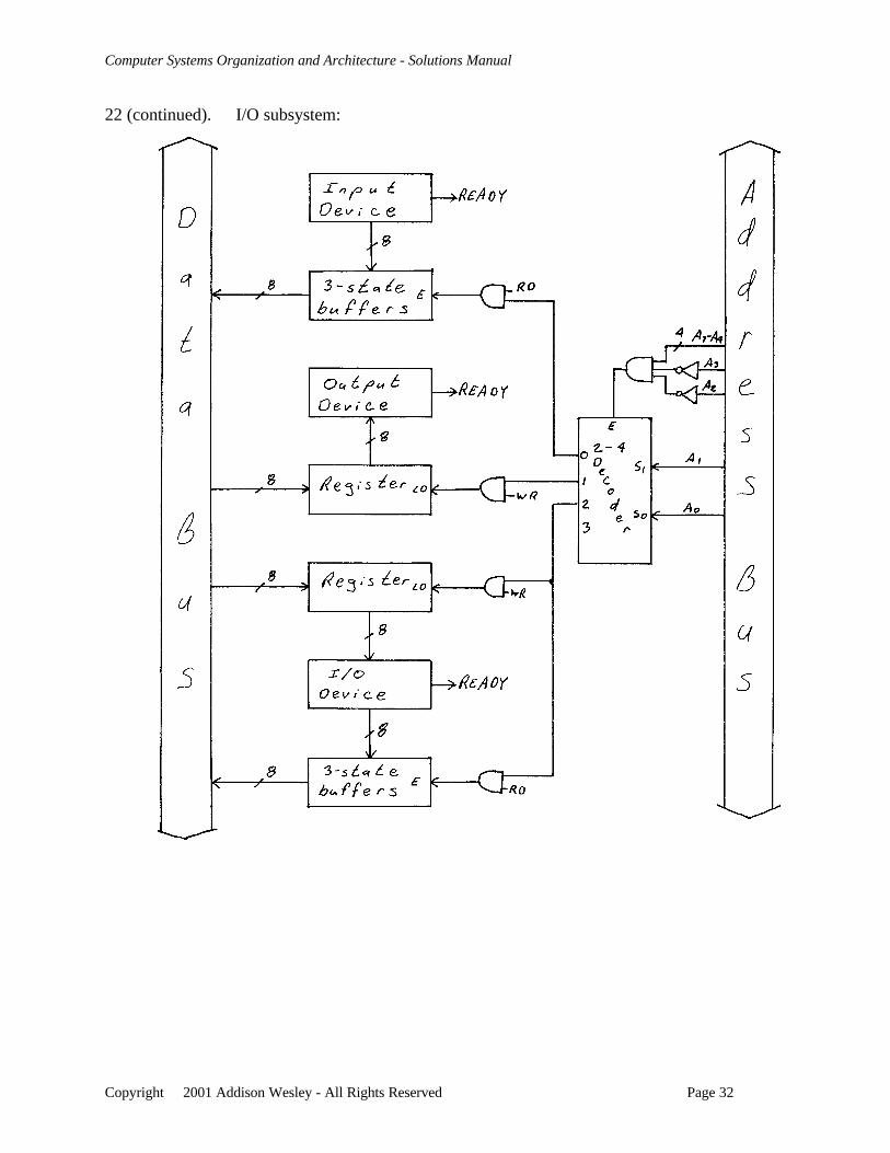
22 (continued). I/O subsystem:
Computer Systems Organization and Architecture - Solutions Manual
Copyright 2001 Addison Wesley - All Rights Reserved Page 33
Chapter 5
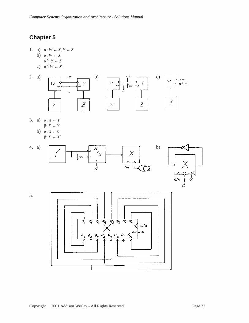
1. a) α: W ← X, Y ← Zb) α: W ← X
α': Y ← Zc) α': W ← X
2. a) b) c)
3. a) α: X ← Yβ: X ← Y'
b) α: X ← 0β: X ← X'
4. a) b)
5.
Computer Systems Organization and Architecture - Solutions Manual
Copyright 2001 Addison Wesley - All Rights Reserved Page 34
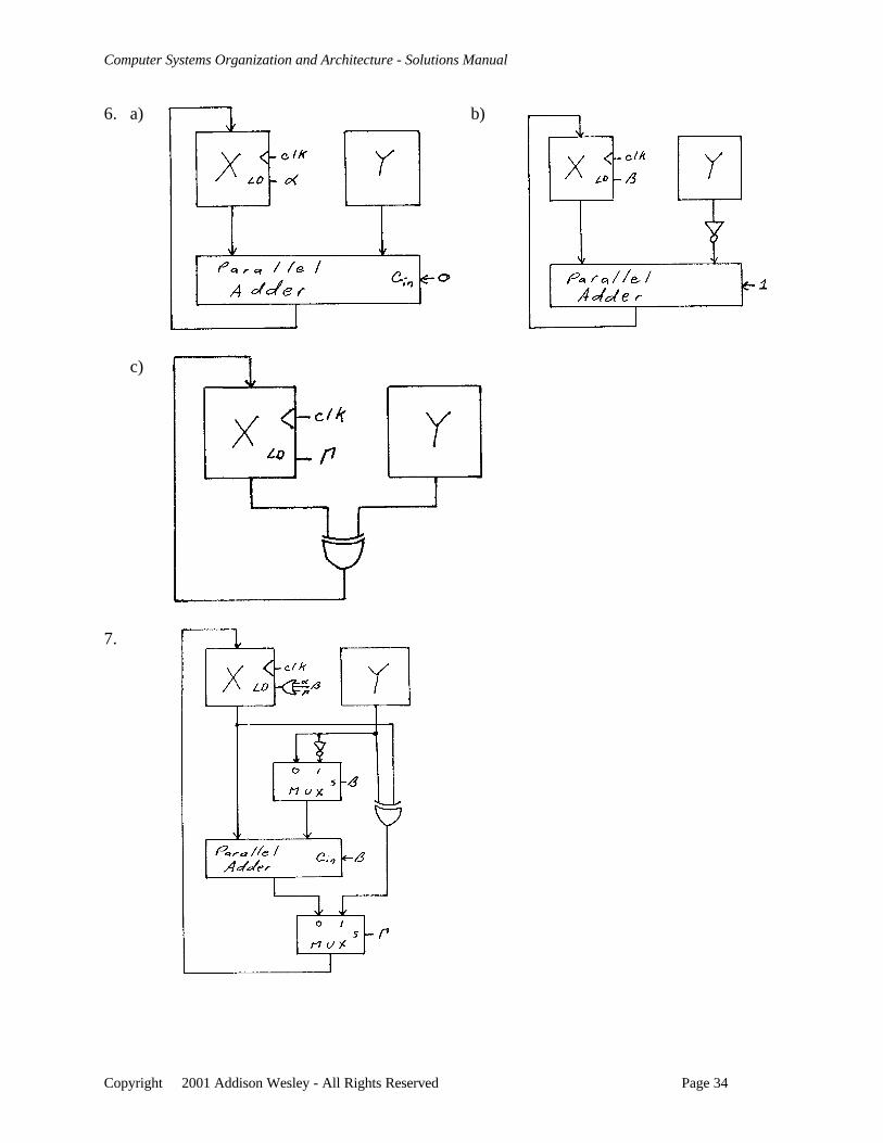
6. a) b)
c)
7.
Computer Systems Organization and Architecture - Solutions Manual
Copyright 2001 Addison Wesley - All Rights Reserved Page 35
8. a) 0011 0010 0000 0100b) 0100 1100 1000 0001c) 0011 0010 0000 0101d) 0100 1100 1000 0001e) 1011 0010 0000 0100f) 1100 1100 1000 0001g) 1001 0000 0010 0000h) 0000 1001 1001 0000
9. a) 0000 0111 0010 1010b) 0100 0001 1100 1010c) 0000 0111 0010 1011d) 1100 0001 1100 1010e) 1000 0111 0010 1010f) 1100 0001 1100 1010g) 0011 1001 0101 0000h) 0000 1000 0011 1001
10. a) 1011 0010 1111 0000b) 0010 1100 1011 1100c) 1011 0010 1111 0000d) 0010 1100 1011 1100e) 0011 0010 1111 0000f) 0010 1100 1011 1100g) 1001 0111 1000 0000h) 0000 0101 1001 0111
Computer Systems Organization and Architecture - Solutions Manual
Copyright 2001 Addison Wesley - All Rights Reserved Page 36
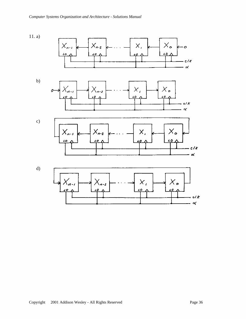
11. a)
b)
c)
d)
Computer Systems Organization and Architecture - Solutions Manual
Copyright 2001 Addison Wesley - All Rights Reserved Page 37
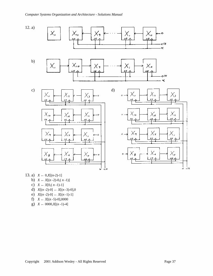
12. a)
b)
c) d)
13. a) X ← 0,X[(n-2)-1]b) X ← X[(n -2)-0,( n -1)]c) X ← X[0,( n -1)-1]d) X[(n -2)-0] ← X[(n -3)-0],0e) X[(n -2)-0] ← X[(n -1)-1]f) X ← X[(n -5)-0],0000g) X ← 0000,X[(n -1)-4]
Computer Systems Organization and Architecture - Solutions Manual
Copyright 2001 Addison Wesley - All Rights Reserved Page 38
14. Define X1X0 = 00 (S0), 01 (S1), 10 (S2), 11 (S3). I is the input bit.
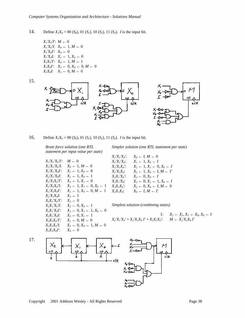
X1'X0'I': M ← 0X1'X0'I: X0 ← 1, M ← 0X1'X0I': X0 ← 0X1'X0I: X1 ← 1, X0 ← 0X1X0'I': X0 ← 1, M ← 1X1X0I': X1 ← 0, X0 ← 0, M ← 0X1X0I: X1 ← 0, M ← 0
15.
16. Define X1X0 = 00 (S0), 01 (S1), 10 (S2), 11 (S3). I is the input bit.
Brute force solution (one RTLstatement per input value per state)
X2'X1'X0'I': M ← 0X2'X1'X0'I: X0 ← 1, M ← 0X2'X1'X0I': X1 ← 1, X0 ← 0X2'X1'X0I: X1 ← 1, X0 ← 1X2'X1X0'I': X2 ← 1, X1 ← 0X2'X1X0'I: X2 ← 1, X1 ← 0, X0 ← 1X2'X1X0I': X2 ← 1, X0 ← 0, M ← 1X2'X1X0I: X2 ← 1X2X1'X0'I': X2 ← 0X2X1'X0'I: X2 ← 0, X0 ← 1X2X1'X0I': X2 ← 0, X1 ← 1, X0 ← 0X2X1'X0I: X2 ← 0, X1 ← 1X2X1X0'I': X1 ← 0, M ← 0X2X1X0'I: X1 ← 0, X0 ← 1, M ← 0X2X1X0I': X0 ← 0
Simpler solution (one RTL statement per state)
X2'X1'X0': X0 ← I, M ← 0X2'X1'X0: X1 ← 1, X0 ← IX2'X1X0': X2 ← 1, X1 ← 0, X0 ← IX2'X1X0: X2 ← 1, X0 ← I, M ← I'X2X1'X0': X2 ← 0, X0 ← IX2X1'X0: X2 ← 0, X1 ← 1, X0 ← IX2X1X0': X1 ← 0, X0 ← I, M ← 0X2X1X0: X0 ← I, M ← I'
Simplest solution (combining states)
1: X2 ← X1, X1 ← X0, X0 ← IX2'X1'X0' + X2'X1X0 I' + X2X1X0': M ← X2'X1X0 I'
17.
Computer Systems Organization and Architecture - Solutions Manual
Copyright 2001 Addison Wesley - All Rights Reserved Page 39
18. library IEEE;use IEEE.std_logic_1164.all;
entity string_checker isport(
I,clk: in std_logic;M: out std_logic
);end string_checker;
architecture a_string_checker of string_checker istype states is (S0, S1, S2, S3);signal present_state, next_state: states;
beginstate_check_string: process(present_state,I)
begincase present_state is
when S0 => M<='0';if (I='0') then next_state <= S0;
else next_state <= S1;end if;
when S1 => M<='0';if (I='0') then next_state <= S0;
else next_state <= S2;end if;
when S2 => M<='0';if (I='0') then next_state <= S3;
else next_state <= S2;end if;
when S3 => M<='1';if (I='0') then next_state <= S0;
else next_state <= S1;end if;
end case;end process state_check_string;
state_transition: process(clk)begin
if rising_edge(clk) then present_state <= next_state;end if;
end process state_transition;
end a_string_checker;
Computer Systems Organization and Architecture - Solutions Manual
Copyright 2001 Addison Wesley - All Rights Reserved Page 40
19. library IEEE;use IEEE.std_logic_1164.all;
entity string_checker isport(
I,clk: in std_logic;X1,X0: buffer std_logic;
M: out std_logic);
end string_checker;
architecture a_string_checker of string_checker isbegin
cct_string_checker: process(X1,X0,I,clk)begin
if rising_edge(clk) thenX1 <= (X1 and (not X0)) or
((not X1) and X0 and I);X0 <= ((not X1) and (not X0) and I) or
(X1 and (not X0) and (not I)) or (X1 and X0 and I);
end if; M <= X1 AND X0;
end process cct_string_checker;end a_string_checker;
Computer Systems Organization and Architecture - Solutions Manual
Copyright 2001 Addison Wesley - All Rights Reserved Page 41
20. library IEEE;use IEEE.std_logic_1164.all;
entity string_checker isport(
I,clk: in std_logic;M: out std_logic
);end string_checker;
architecture a_string_checker of string_checker istype states is (S0, S1, S2, S3, S4, S5, S6, S7);signal present_state, next_state: states;
beginstate_check_string: process(present_state,I)
begincase present_state is
when S0 => M<='0';if (I='0') then next_state <= S0;
else next_state <= S1;end if;
when S1 => M<='0';if (I='0') then next_state <= S2;
else next_state <= S3;end if;
when S2 => M<='0';if (I='0') then next_state <= S4;
else next_state <= S5;end if;
when S3 => M<='0';if (I='0') then next_state <= S6;
else next_state <= S7;end if;
when S4 => M<='0';if (I='0') then next_state <= S0;
else next_state <= S1;end if;
when S5 => M<='0';if (I='0') then next_state <= S2;
else next_state <= S3;end if;
when S6 => M<='1';if (I='0') then next_state <= S4;
else next_state <= S5;end if;
when S7 => M<='0';if (I='0') then next_state <= S6;
else next_state <= S7;end if;
end case;end process state_check_string;
state_transition: process(clk)begin
if rising_edge(clk) then present_state <= next_state;end if;
end process state_transition;
end a_string_checker;
Computer Systems Organization and Architecture - Solutions Manual
Copyright 2001 Addison Wesley - All Rights Reserved Page 42
21. library IEEE;use IEEE.std_logic_1164.all;
entity string_checker isport(
I,clk: in std_logic;X2,X1,X0: buffer std_logic;
M: out std_logic);
end string_checker;
architecture a_string_checker of string_checker isbegin
cct_string_checker: process(X1,X0,I,clk)begin
if rising_edge(clk) thenX2 <= X1;X1 <= X0;X0 <= I;
end if; M <= X2 and X1 and (not X0);
end process cct_string_checker;end a_string_checker;
22. library IEEE;use IEEE.std_logic_1164.all;
entity toll_booth_controller isport(
I1,I0,C,clk: in std_logic; R,G,A: out std_logic
);end toll_booth_controller;
architecture a_toll_booth_controller of toll_booth_controller istype states is (SN, S0, S5, S10, S15, S20, S25, S30, SP, SC);signal present_state, next_state: states;
beginstate_toll_booth_controller: process(present_state,I1,I0)
begincase present_state is
when SN => R<='1'; G<='0'; A<='0';if (C='1') then next_state <= S0;
else next_state <= SN;end if;
when S0 => R<='1'; G<='0'; A<='0';if (C='0') then next_state <= SC;
elsif (I1 = '0' AND I0 = '1') then next_state <= S5;elsif (I1 = '1' AND I0 = '0') then next_state <= S10;elsif (I1 = '1' AND I0 = '1') then next_state <= S25;else next_state <= S0;
end if;when S5 => R<='1'; G<='0'; A<='0';
if (C='0') then next_state <= SC;elsif (I1 = '0' AND I0 = '1') then next_state <= S10;elsif (I1 = '1' AND I0 = '0') then next_state <= S15;elsif (I1 = '1' AND I0 = '1') then next_state <= S30;else next_state <= S5;
end if;
Computer Systems Organization and Architecture - Solutions Manual
Copyright 2001 Addison Wesley - All Rights Reserved Page 43
when S10 => R<='1'; G<='0'; A<='0';if (C='0') then next_state <= SC;
elsif (I1 = '0' AND I0 = '1') then next_state <= S15;elsif (I1 = '1' AND I0 = '0') then next_state <= S20;elsif (I1 = '1' AND I0 = '1') then next_state <= SP;else next_state <= S10;
end if;when S15 => R<='1'; G<='0'; A<='0';
if (C='0') then next_state <= SC;elsif (I1 = '0' AND I0 = '1') then next_state <= S20;elsif (I1 = '1' AND I0 = '0') then next_state <= S25;elsif (I1 = '1' AND I0 = '1') then next_state <= SP;else next_state <= S15;
end if;when S20 => R<='1'; G<='0'; A<='0';
if (C='0') then next_state <= SC;elsif (I1 = '0' AND I0 = '1') then next_state <= S25;elsif (I1 = '1' AND I0 = '0') then next_state <= S30;elsif (I1 = '1' AND I0 = '1') then next_state <= SP;else next_state <= S20;
end if;when S25 => R<='1'; G<='0'; A<='0';
if (C='0') then next_state <= SC;elsif (I1 = '0' AND I0 = '1') then next_state <= S30;elsif (I1 = '1') then next_state <= SP;else next_state <= S25;
end if;when S30 => R<='1'; G<='0'; A<='0';
if (C='0') then next_state <= SC;elsif (I1 = '1' OR I0 = '1') then next_state <= SP;else next_state <= S30;
end if;when SP => R<='0'; G<='1'; A<='0';
if (C='0') then next_state <= SN;else next_state <= SP;
end if;when SC => R<='1'; G<='0'; A<='1';
if (C='1') then next_state <= S0;else next_state <= SC;
end if;end case;
end process state_toll_booth_controller;
state_transition: process(clk)begin
if rising_edge(clk) then present_state <= next_state;end if;
end process state_transition;
end a_toll_booth_controller;
Computer Systems Organization and Architecture - Solutions Manual
Copyright 2001 Addison Wesley - All Rights Reserved Page 44
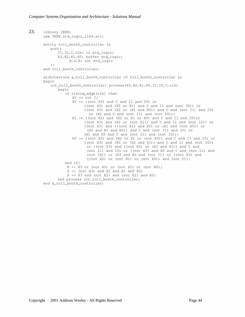
23. library IEEE;use IEEE.std_logic_1164.all;
entity toll_booth_controller isport(
I1,I0,C,clk: in std_logic;X3,X2,X1,X0: buffer std_logic;
R,G,A: out std_logic);
end toll_booth_controller;
architecture a_toll_booth_controller of toll_booth_controller isbegin
cct_toll_booth_controller: process(X3,X2,X1,X0,I1,I0,C,clk)begin
if rising_edge(clk) thenX3 <= not C;X2 <= ((not X3) and C and I1 and I0) or
((not X3) and (X2 or X1) and C and I1 and (not I0)) or ((not X3) and (X2 or (X1 and X0)) and C and (not I1) and I0)
or (X2 and C and (not I1) and (not I0));X1 <= ((not X3) and (X2 or X1 or X0) and C and I1 and I0)or
((not X3) and (X2 or (not X1)) and C and I1 and (not I0)) or ((not X3) and (((not X1) and X0) or (X1 and (not X0)) or
(X2 and X1 and X0)) and C and (not I1) and I0) or (X1 and X0 and C and (not I1) and (not I0));
X0 <= ((not X3) and (X2 or X1 or (not X0)) and C and I1 and I0) or ((not X3) and (X0 or (X2 and X1)) and C and I1 and (not I0))
or ((not X3) and ((not X0) or (X2 and X1)) and C and(not I1) and I0) or ((not X3) and X0 and C and (not I1) and(not I0)) or (X3 and X0 and (not C)) or ((not X3) and((not X2) or (not X1) or (not X0)) and (not C));
end if; R <= X3 or (not X2) or (not X1) or (not X0); G <= (not X3) and X2 and X1 and X0; A <= X3 and (not X2) and (not X1) and X0;
end process cct_toll_booth_controller;end a_toll_booth_controller;
Computer Systems Organization and Architecture - Solutions Manual
Copyright 2001 Addison Wesley - All Rights Reserved Page 45
Chapter 6
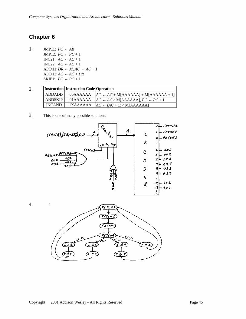
1. JMP11: PC ← ARJMP12: PC ← PC + 1INC21: AC ← AC + 1INC22: AC ← AC + 1ADD11: DR ← M, AC ← AC + 1ADD12: AC ← AC + DRSKIP1: PC ← PC + 1
2. Instruction Instruction Code OperationADDADD 00AAAAAA AC ← AC + M[AAAAAA] + M[AAAAAA + 1]ANDSKIP 01AAAAAA AC ← AC ^ M[AAAAAA], PC ← PC + 1INCAND 1XAAAAAA AC ← (AC + 1) ^ M[AAAAAA]
3. This is one of many possible solutions.
4.
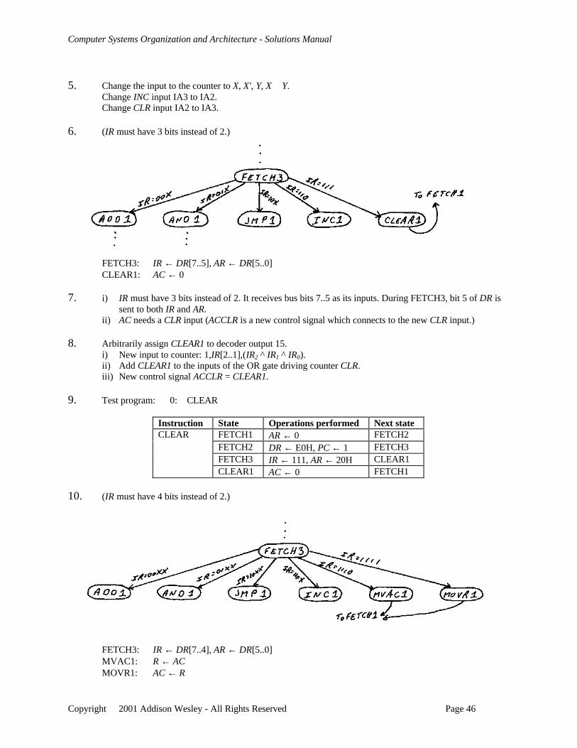
Computer Systems Organization and Architecture - Solutions Manual
Copyright 2001 Addison Wesley - All Rights Reserved Page 46
5. Change the input to the counter to X, X', Y, X ∨ Y.Change INC input IA3 to IA2.Change CLR input IA2 to IA3.
6. (IR must have 3 bits instead of 2.)
FETCH3: IR ← DR[7..5], AR ← DR[5..0]CLEAR1: AC ← 0
7. i) IR must have 3 bits instead of 2. It receives bus bits 7..5 as its inputs. During FETCH3, bit 5 of DR issent to both IR and AR.
ii) AC needs a CLR input (ACCLR is a new control signal which connects to the new CLR input.)
8. Arbitrarily assign CLEAR1 to decoder output 15.i) New input to counter: 1,IR[2..1],(IR2 ^ IR1 ^ IR0).ii) Add CLEAR1 to the inputs of the OR gate driving counter CLR.iii) New control signal ACCLR = CLEAR1.
9. Test program: 0: CLEAR
Instruction State Operations performed Next stateCLEAR FETCH1 AR ← 0 FETCH2
FETCH2 DR ← E0H, PC ← 1 FETCH3FETCH3 IR ← 111, AR ← 20H CLEAR1CLEAR1 AC ← 0 FETCH1
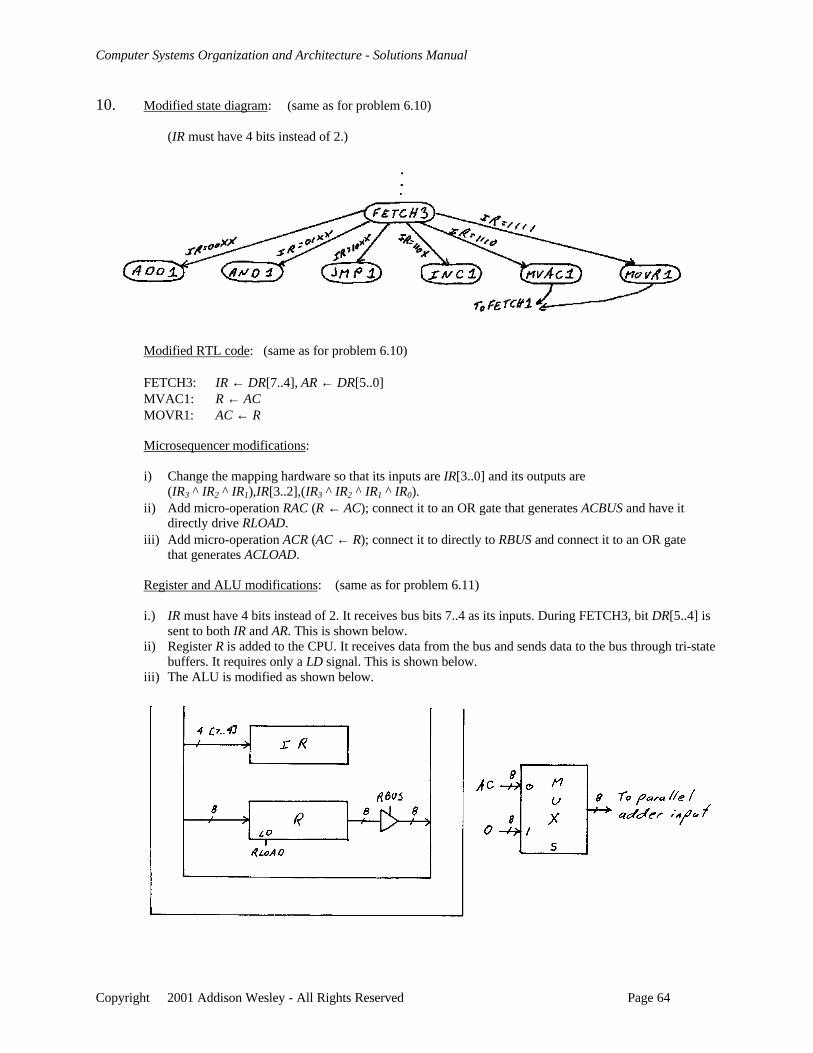
10. (IR must have 4 bits instead of 2.)
FETCH3: IR ← DR[7..4], AR ← DR[5..0]MVAC1: R ← ACMOVR1: AC ← R
Computer Systems Organization and Architecture - Solutions Manual
Copyright 2001 Addison Wesley - All Rights Reserved Page 47
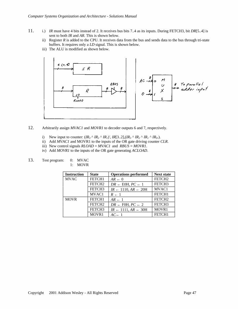
11. i.) IR must have 4 bits instead of 2. It receives bus bits 7..4 as its inputs. During FETCH3, bit DR[5..4] issent to both IR and AR. This is shown below.
ii) Register R is added to the CPU. It receives data from the bus and sends data to the bus through tri-statebuffers. It requires only a LD signal. This is shown below.
iii) The ALU is modified as shown below.
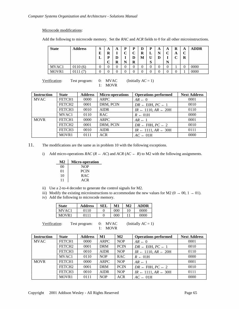
12. Arbitrarily assign MVAC1 and MOVR1 to decoder outputs 6 and 7, respectively.
i) New input to counter: (IR3 ^ IR2 ^ IR1)', IR[3..2],(IR3 ^ IR2 ^ IR1 ^ IR0.).ii) Add MVAC1 and MOVR1 to the inputs of the OR gate driving counter CLR.iii) New control signals RLOAD = MVAC1 and RBUS = MOVR1.iv) Add MOVR1 to the inputs of the OR gate generating ACLOAD.
13. Test program: 0: MVAC1: MOVR
Instruction State Operations performed Next stateMVAC FETCH1 AR ← 0 FETCH2
FETCH2 DR ← E0H, PC ← 1 FETCH3FETCH3 IR ← 1110, AR ← 20H MVAC1MVAC1 R ← 1 FETCH1
MOVR FETCH1 AR ← 1 FETCH2FETCH2 DR ← F0H, PC ← 2 FETCH3FETCH3 IR ← 1111, AR ← 30H MOVR1MOVR1 AC← 1 FETCH1
Computer Systems Organization and Architecture - Solutions Manual
Copyright 2001 Addison Wesley - All Rights Reserved Page 48
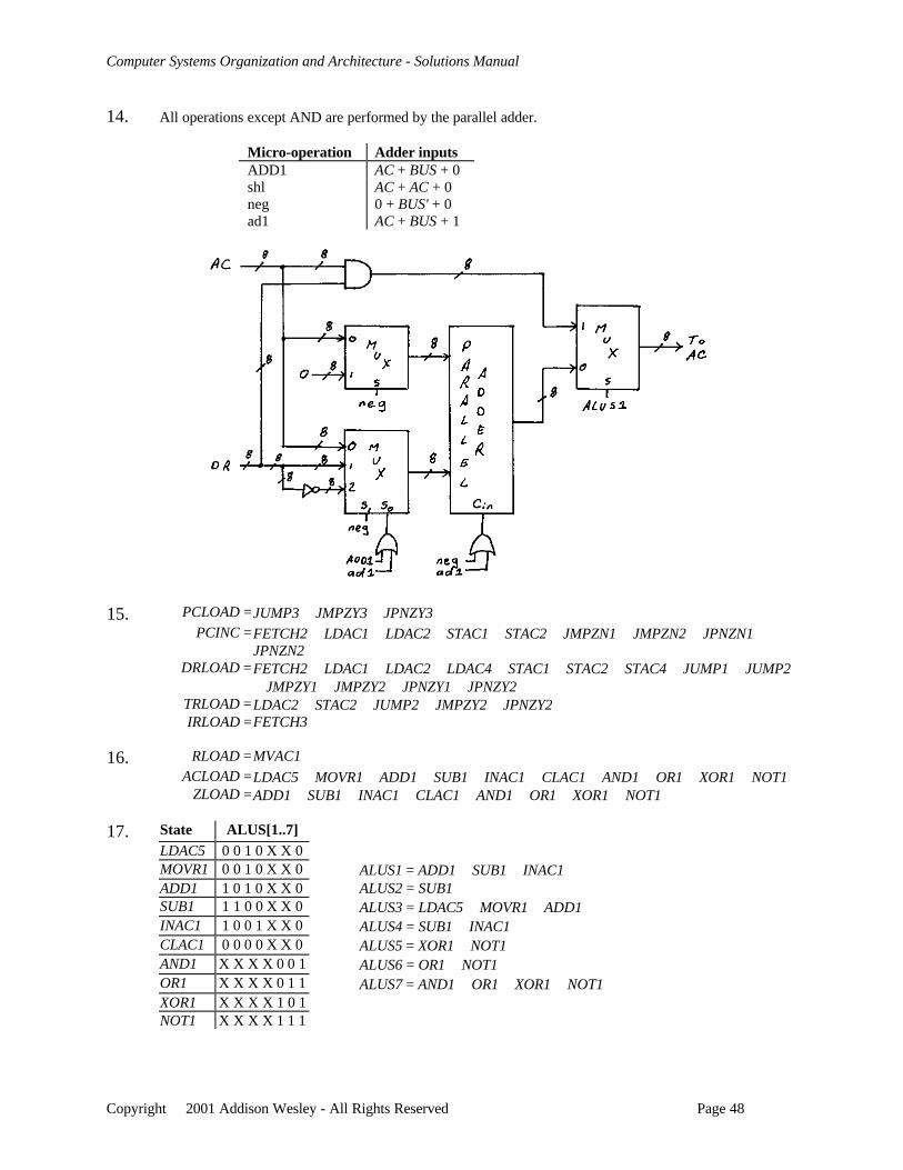
14. All operations except AND are performed by the parallel adder.
Micro-operation Adder inputsADD1 AC + BUS + 0shl AC + AC + 0neg 0 + BUS' + 0ad1 AC + BUS + 1
15. PCLOAD =JUMP3 ∨ JMPZY3 ∨ JPNZY3PCINC =FETCH2 ∨ LDAC1 ∨ LDAC2 ∨ STAC1 ∨ STAC2 ∨ JMPZN1 ∨ JMPZN2 ∨ JPNZN1 ∨
JPNZN2DRLOAD =FETCH2 ∨ LDAC1 ∨ LDAC2 ∨ LDAC4 ∨ STAC1 ∨ STAC2 ∨ STAC4 ∨ JUMP1 ∨ JUMP2
∨ JMPZY1 ∨ JMPZY2 ∨ JPNZY1 ∨ JPNZY2TRLOAD =LDAC2 ∨ STAC2 ∨ JUMP2 ∨ JMPZY2 ∨ JPNZY2IRLOAD =FETCH3
16. RLOAD =MVAC1ACLOAD =LDAC5 ∨ MOVR1 ∨ ADD1 ∨ SUB1 ∨ INAC1 ∨ CLAC1 ∨ AND1 ∨ OR1 ∨ XOR1 ∨ NOT1
ZLOAD =ADD1 ∨ SUB1 ∨ INAC1 ∨ CLAC1 ∨ AND1 ∨ OR1 ∨ XOR1 ∨ NOT1
17. State ALUS[1..7]LDAC5 0 0 1 0 X X 0MOVR1 0 0 1 0 X X 0 ALUS1 = ADD1 ∨ SUB1 ∨ INAC1ADD1 1 0 1 0 X X 0 ALUS2 = SUB1SUB1 1 1 0 0 X X 0 ALUS3 = LDAC5 ∨ MOVR1 ∨ ADD1INAC1 1 0 0 1 X X 0 ALUS4 = SUB1 ∨ INAC1CLAC1 0 0 0 0 X X 0 ALUS5 = XOR1 ∨ NOT1AND1 X X X X 0 0 1 ALUS6 = OR1 ∨ NOT1OR1 X X X X 0 1 1 ALUS7 = AND1 ∨ OR1 ∨ XOR1 ∨ NOT1XOR1 X X X X 1 0 1NOT1 X X X X 1 1 1
Computer Systems Organization and Architecture - Solutions Manual
Copyright 2001 Addison Wesley - All Rights Reserved Page 49
18. The student can execute the following program using the Relatively Simple CPU simulator to verify thateach instruction performs properly.
0: LDAC 0000 (AC ← 1)NOPMVAC (R ← 1)ADD (AC ← 2, Z ← 0)INAC (AC ← 3, Z ← 0)XOR (AC ← 2, Z ← 0)AND (AC ← 0, Z ← 1)
9: JMPZ 000D (jump is taken)NOP (skipped by JMPZ 000D)
D: JPNZ 0009 (jump is not taken)NOT (AC ← FF, Z ← 0)JMPZ 0009 (jump is not taken)JPNZ 0018 (jump is taken)NOP (skipped by JMPZ 0018)
18: CLAC (AC ← 0, Z ← 1)OR (AC ← 1, Z ← 0)SUB (AC ← 0, Z ← 1)MOVR (AC ← 1)STAC 0030 (M[30] ← 1)AND (AC ← 1, Z ← 0)JUMP 0000 (start again)
19. SETR1: R ← 0SETR2: R ← R - 1
20. R needs two additional inputs: CLR, driven by new control signal RCLR, and DCR, driven by new controlsignal RDCR.
21. i.) Add hardware to generate ISETR = I7' ^ I6' ^ I5' ^ I4 ^ I3' ^ I2' ^ I1' ^ I0', SETR1 = ISETR ^ T3, andSETR2 = ISETR ^ T4.
ii) Add SETR1 to the OR gate driving INC of the time counter and SETR2 to the OR gate driving CLR ofthe time counter.
iii) New control signals RCLR = SETR1 and RDCR = SETR2.
22. Test program: 0: SETR
Instruction State Operations performed Next stateSETR FETCH1 AR ← 0 FETCH2
FETCH2 DR ← 11H, PC ← 1 FETCH3FETCH3 IR ← 11, AR ← 1 SETR1SETR1 R ← 0 SETR2SETR2 R ←FF FETCH1
Computer Systems Organization and Architecture - Solutions Manual
Copyright 2001 Addison Wesley - All Rights Reserved Page 50
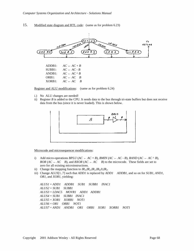
23.
ADDB1: AC ← AC + BSUBB1: AC ← AC - BANDB1: AC ← AC ^ BORB1: AC ← AC ∨ BXORB1: AC ← AC ⊕ B
24. i.) No ALU changes are needed!ii) Register B is added to the CPU. It sends data to the bus through tri-state buffers but does not receive
data from the bus (since it is never loaded). This is shown below.
25. i.) Add the hardware shown below to generate IADDB, ISUBB, IANDB, IORB, and IXORB, and addhardware to generate ADDB1 = IADDB ^ T3, SUBB1 = ISUBB ^ T3, ANDB1 = IANDB ^ T3,ORB1 = IORB ^ T3, and XORB1 = IXORB ^ T3.
ii) OR together ADDB1, SUBB1, ANDB1, ORB1, and XORB1 to generate BBUS.iii) Add the same five signals to the OR gate driving CLR of the counter.iv) Change ALUS[1..7] such that ADD1 is replaced by ADD1 ∨ ADDB1, and so on for SUB1, AND1,
OR1, and XOR1, yielding:
ALUS1 = ADD1 ∨ ADDB1 ∨ SUB1 ∨ SUBB1 ∨ INAC1ALUS2 = SUB1 ∨ SUBB1ALUS3 = LDAC5 ∨ MOVR1 ∨ ADD1∨ ADDB1ALUS4 = SUB1 ∨ SUBB1∨ INAC1ALUS5 = XOR1 ∨ XORB1 ∨ NOT1ALUS6 = OR1 ∨ ORB1 ∨ NOT1ALUS7 = AND1 ∨ ANDB1 ∨ OR1 ∨ ORB1 ∨ XOR1 ∨ XORB1 ∨ NOT1
Computer Systems Organization and Architecture - Solutions Manual
Copyright 2001 Addison Wesley - All Rights Reserved Page 51
26. Initially AC = 1 and B = 2. Fetch cycles not shown.
Instruction State Operations performedORB ORB1 AC ← 1 ∨ 2 = 3ADDB ADDB1 AC ← 3 + 2 = 5ANDB ANDB1 AC ← 5 ^ 2 = 0XORB XORB1 AC ← 0 ⊕ 2 = 2SUBB SUBB1 AC ← 2 - 2 = 0
27. i.) Remove CLAC1 and INAC1 as inputs to the OR gate which generates ACLOAD.ii) Add control inputs to AC: CLR = CLAC1, and INC = INAC1.iii) Change the input to Z as shown below. ZLOAD is unchanged.
28. State diagram and RTL code:
FETCH1: AR ← PCFETCH2: DR ← M, PC ← PC + 1FETCH3: IR ← DR[7..6], AR ← DR[5..0]COM1: AC ← AC'JREL1: DR ← MJREL2: PC ← PC + DR[5..0]OR1: DR ← MOR2: AC ← AC ∨ DRSUB11: DR ← MSUB12: AC ← AC + DR'
The register section is the same as Figure 6.6, except for the data input to PC, shown below.
Computer Systems Organization and Architecture - Solutions Manual
Copyright 2001 Addison Wesley - All Rights Reserved Page 52
Control signals: ARLOAD =FETCH1 ∨ FETCH3PCLOAD =JREL2
PCINC =FETCH2PCBUS =FETCH1
DRLOAD = MEMBUS = READ =FETCH2 ∨ JREL1∨ OR1∨ SUB11DRBUS =FETCH3 ∨ JREL2 ∨ OR2 ∨ SUB12
ACLOAD =COM1 ∨ OR2 ∨ SUB12IRLOAD =FETCH3
ALU:
Control unit:
Computer Systems Organization and Architecture - Solutions Manual
Copyright 2001 Addison Wesley - All Rights Reserved Page 53
29. State diagram and RTL code:
FETCH1: AR ← PC ADD1: DR ← M, PC ← PC + 1FETCH2: DR ← M, PC ← PC + 1 ADD2: AC ← AC + DRFETCH3: IR ← DR[7..5], AR ← PC OR1: DR ← M, PC ← PC + 1LDI1: DR ← M, PC ← PC + 1 OR2: AC ← AC ∨ DRLDI2: AC ← DR JUMP1: DR ← MSTO1: DR ← M, PC ← PC + 1 JUMP2: PC ← DRSTO2: AR ← DR JREL1: PC ← PC + 000DR[4..0]STO3: DR ← AC SKIP1: PC ← PC + 1STO4: M ← DR RST1: PC ← 0, AC ← 0
Control signals: ARLOAD =FETCH1 ∨ FETCH3 ∨ STO2PCLOAD =JUMP2 ∨ JREL2
PCINC =FETCH2 ∨ LDI1 ∨ STO1 ∨ ADD1 ∨ OR1 ∨ SKIP1PCCLR =RST1
PCBUS =FETCH1 ∨ FETCH3PCMUX =JUMP2DRLOAD =FETCH2 ∨ LDI1 ∨ STO1 ∨ STO3 ∨ ADD1 ∨ OR1 ∨ JUMP1
DRBUS =FETCH3 ∨ LDI2 ∨ STO2 ∨ STO4 ∨ ADD2 ∨ OR2 ∨ JUMP2 ∨ JREL1ACLOAD =LDI2 ∨ ADD2 ∨ OR2
ACCLR =RST1ACBUS =STO3
IRLOAD =FETCH3MEMBUS = READ =FETCH2 ∨ LDI1 ∨ STO1 ∨ ADD1 ∨ OR1 ∨ JUMP1
BUSMEM = WRITE =STO4
Computer Systems Organization and Architecture - Solutions Manual
Copyright 2001 Addison Wesley - All Rights Reserved Page 54
Register section:
ALU:
Computer Systems Organization and Architecture - Solutions Manual
Copyright 2001 Addison Wesley - All Rights Reserved Page 55
Control unit:
FETCH1 = T0 ADD1 = IADD ^ T3FETCH2 = T1 ADD2 = IADD ^ T4FETCH3 = T2 OR1 = IOR ^ T3
LDI1 = ILDI ^ T3 OR2 = IOR ^ T4LDI2 = ILDI ^ T4 JUMP1 = IJUMP ^ T3STO1 = ISTO ^ T3 JUMP2 = IJUMP ^ T4STO2 = ISTO ^ T4 JREL1 = IJREL ^ T3STO3 = ISTO ^ T5 JREL2 = IJREL ^ T4STO4 = ISTO ^ T6 SKIP1 = ISKIP ^ T3
RST1 = IRST ^ T3
30. Modified state diagram:
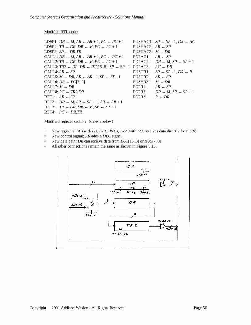
Computer Systems Organization and Architecture - Solutions Manual
Copyright 2001 Addison Wesley - All Rights Reserved Page 56
Modified RTL code:
LDSP1: DR ← M, AR ← AR + 1, PC ← PC + 1 PUSHAC1: SP ← SP - 1, DR ← ACLDSP2: TR ← DR, DR ← M, PC ← PC + 1 PUSHAC2: AR ← SPLDSP3: SP ← DR,TR PUSHAC3: M ← DRCALL1: DR ← M, AR ← AR + 1, PC ← PC + 1 POPAC1: AR ← SPCALL2: TR ← DR, DR ← M, PC ← PC + 1 POPAC2: DR ← M, SP ← SP + 1CALL3: TR2 ← DR, DR ← PC[15..8], SP ← SP - 1 POPAC3: AC ← DRCALL4: AR ← SP PUSHR1: SP ← SP - 1, DR ← RCALL5: M ← DR, AR ← AR - 1, SP ← SP - 1 PUSHR2: AR ← SPCALL6: DR ← PC[7..0] PUSHR3: M ← DRCALL7: M ← DR POPR1: AR ← SPCALL8: PC ← TR2,DR POPR2: DR ← M, SP ← SP + 1RET1: AR ← SP POPR3: R ← DRRET2: DR ← M, SP ← SP + 1, AR ← AR + 1RET3: TR ← DR, DR ← M, SP ← SP + 1RET4: PC ← DR,TR
Modified register section: (shown below)
• New registers: SP (with LD, DEC, INC), TR2 (with LD, receives data directly from DR)• New control signal: AR adds a DEC signal• New data path: DR can receive data from BUS[15..8] or BUS[7..0]• All other connections remain the same as shown in Figure 6.15.
Computer Systems Organization and Architecture - Solutions Manual
Copyright 2001 Addison Wesley - All Rights Reserved Page 57
New control signals:
ARDEC = CALL5SPLOAD = LDSP3
SPINC = RET2 ∨ RET3 ∨ POPAC2 ∨ POPR2SPDEC = CALL3 ∨ CALL5 ∨ PUSHAC1 ∨ PUSHR1SPBUS = CALL4 ∨ RET1 ∨ PUSHAC2 ∨ POPAC1 ∨ PUSHR2 ∨ POPR1DRSEL = CALL3
TR2LOAD = CALL3TR2BUS = CALL8
Modified control signals:
ARLOAD = (original value) ∨ CALL4 ∨ RET1 ∨ PUSHAC2 ∨ POPAC1 ∨PUSHR2 ∨ POPR1
ARINC = (original value) ∨ LDSP1 ∨ CALL1 ∨ RET2PCLOAD = (original value) ∨ CALL8 ∨ RET4
PCINC = (original value) ∨ LDSP1 ∨ LDSP2 ∨ CALL1 ∨ CALL2PCBUS = (original value) ∨ CALL3 ∨ CALL6
DRLOAD = (original value) ∨ LDSP1 ∨ LDSP2 ∨ CALL1 ∨ CALL2 ∨CALL3 ∨ CALL6 ∨ RET2 ∨ RET3 ∨ PUSHAC1 ∨ POPAC2 ∨PUSHR1 ∨ POPR2
DRHBUS = (original value) ∨ LDSP3 ∨ RET4DRLBUS = (original value) ∨ CALL5 ∨ CALL7 ∨ PUSHAC3 ∨ POPAC3 ∨
PUSHR3 ∨ POPR3TRLOAD = (original value) ∨ LDSP2 ∨ CALL2 ∨ RET3
TRBUS = (original value) ∨ LDSP3 ∨ CALL8 ∨ RET4RLOAD = (original value) ∨ POPR3
RBUS = (original value) ∨ PUSHR1ACLOAD = (original value) ∨ POPAC3
ACBUS = (original value) ∨ PUSHAC1ALUS1 = (original value) ∨ POPAC3
MEMBUS = (original value) ∨ LDSP1 ∨ LDSP2 ∨ CALL1 ∨ CALL2 ∨ RET2∨ RET3 ∨ POPAC2 ∨ POPR2
BUSMEM = (original value) ∨ CALL5 ∨ CALL7 ∨ PUSHAC3 ∨ PUSHR3WRITE = (original value) ∨ CALL5 ∨ CALL7 ∨ PUSHAC3 ∨ PUSHR3
Computer Systems Organization and Architecture - Solutions Manual
Copyright 2001 Addison Wesley - All Rights Reserved Page 58
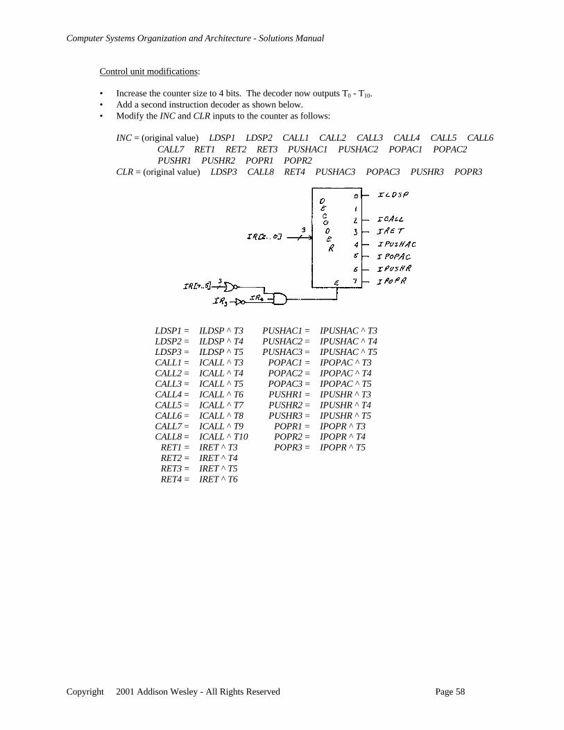
Control unit modifications:
• Increase the counter size to 4 bits. The decoder now outputs T0 - T10.• Add a second instruction decoder as shown below.• Modify the INC and CLR inputs to the counter as follows:
INC = (original value) ∨ LDSP1 ∨ LDSP2 ∨ CALL1 ∨ CALL2 ∨ CALL3 ∨ CALL4 ∨ CALL5 ∨ CALL6∨ CALL7 ∨ RET1 ∨ RET2 ∨ RET3 ∨ PUSHAC1 ∨ PUSHAC2 ∨ POPAC1 ∨ POPAC2∨ PUSHR1 ∨ PUSHR2 ∨ POPR1 ∨ POPR2
CLR = (original value) ∨ LDSP3 ∨ CALL8 ∨ RET4 ∨ PUSHAC3 ∨ POPAC3 ∨ PUSHR3 ∨ POPR3
LDSP1 = ILDSP ^ T3 PUSHAC1 = IPUSHAC ^ T3LDSP2 = ILDSP ^ T4 PUSHAC2 = IPUSHAC ^ T4LDSP3 = ILDSP ^ T5 PUSHAC3 = IPUSHAC ^ T5CALL1 = ICALL ^ T3 POPAC1 = IPOPAC ^ T3CALL2 = ICALL ^ T4 POPAC2 = IPOPAC ^ T4CALL3 = ICALL ^ T5 POPAC3 = IPOPAC ^ T5CALL4 = ICALL ^ T6 PUSHR1 = IPUSHR ^ T3CALL5 = ICALL ^ T7 PUSHR2 = IPUSHR ^ T4CALL6 = ICALL ^ T8 PUSHR3 = IPUSHR ^ T5CALL7 = ICALL ^ T9 POPR1 = IPOPR ^ T3CALL8 = ICALL ^ T10 POPR2 = IPOPR ^ T4
RET1 = IRET ^ T3 POPR3 = IPOPR ^ T5RET2 = IRET ^ T4RET3 = IRET ^ T5RET4 = IRET ^ T6
Computer Systems Organization and Architecture - Solutions Manual
Copyright 2001 Addison Wesley - All Rights Reserved Page 59
Chapter 7
1. IR MAP00 001101 0101 MAP = IR1 ^ IR0, IR1 ⊕ IR0, IR0',(IR1 ^ IR0)'10 011111 1000
2. State Address SEL
ARPC
AIDR
PCIN
PCDR
DRM
PLUS
AND
ACIN
ADDR
FETCH1 0000 (0) 0 1 0 0 0 0 0 0 0 0001
FETCH2 0001 (1) 0 0 0 1 0 1 0 0 0 0010
FETCH3 0010 (2) 1 0 1 0 0 0 0 0 0 XXXX
ADD1 0011 (3) 0 0 0 0 0 1 0 0 0 0100
ADD2 0100 (4) 0 0 0 0 0 0 1 0 0 0000
AND1 0101 (5) 0 0 0 0 0 1 0 0 0 0110
AND2 0110 (6) 0 0 0 0 0 0 0 1 0 0000
JMP1 0111 (7) 0 0 0 0 1 0 0 0 0 0000
INC1 1000 (8) 0 0 0 0 0 0 0 0 1 0000
3. M1 M2NOP NOP Required
DR ← M PC ← PC + 1 Micro-operations in these two rows must beAC ← AC' AC ← AC + 1 allocated the same relative to each other
DR ← DR + 1 PC ← PC + DR[5..0] The remaining operations are assignedAR ← PC arbitrarily
IR,AR ← DRAC ← AC ⊕ DR
M ← DR
Computer Systems Organization and Architecture - Solutions Manual
Copyright 2001 Addison Wesley - All Rights Reserved Page 60
4. Test program: 0: ADD 41: AND 52: INC3: JMP 04: 27H5: 39H
Instruction State Address Micro-operations Operations performed Next AddressADD 4 FETCH1 0000 ARPC AR ← 0 0001
FETCH2 0001 DRM, PCIN DR ← 04H, PC ← 1 0010FETCH3 0010 AIDR IR ← 00, AR ← 04H 1000ADD1 1000 DRM DR ← 27H 1001ADD2 1001 PLUS AC ← 0 + 27H = 27H 0000
AND 5 FETCH1 0000 ARPC AR ← 1 0001FETCH2 0001 DRM, PCIN DR ← 45H, PC ← 2 0010FETCH3 0010 AIDR IR ← 01, AR ← 05H 1010AND1 1010 DRM DR ← 39H 1011AND2 1011 AND AC ← 27H ^ 39H = 31H 0000
INC FETCH1 0000 ARPC AR ← 2 0001FETCH2 0001 DRM, PCIN DR ← C0H, PC ← 3 0010FETCH3 0010 AIDR IR ← 11, AR ← 00H 1110INC1 1110 ACIN AC ← 21H + 1 = 22H 0000
JMP 0 FETCH1 0000 ARPC AR ← 3 0001FETCH2 0001 DRM, PCIN DR ← 80H, PC ← 4 0010FETCH3 0010 AIDR IR ← 10, AR ← 00H 1100JMP1 1100 PCDR PC ← 0 0000
5. Use the same test program as in problem 4.
Instruction State Address M1 M2 Operations performed Next AddressADD 4 FETCH1 0000 ARPC NOP AR ← 0 0001
FETCH2 0001 DRM PCIN DR ← 04H, PC ← 1 0010FETCH3 0010 AIDR NOP IR ← 00, AR ← 04H 1000ADD1 1000 DRM NOP DR ← 27H 1001ADD2 1001 PLUS NOP AC ← 0 + 27H = 27H 0000
AND 5 FETCH1 0000 ARPC NOP AR ← 1 0001FETCH2 0001 DRM PCIN DR ← 45H, PC ← 2 0010FETCH3 0010 AIDR NOP IR ← 01, AR ← 05H 1010AND1 1010 DRM NOP DR ← 39H 1011AND2 1011 AND NOP AC ← 27H ^ 39H = 31H 0000
INC FETCH1 0000 ARPC NOP AR ← 2 0001FETCH2 0001 DRM PCIN DR ← C0H, PC ← 3 0010FETCH3 0010 AIDR NOP IR ← 11, AR ← 00H 1110INC1 1110 ACIN NOP AC ← 21H + 1 = 22H 0000
JMP 0 FETCH1 0000 ARPC NOP AR ← 3 0001FETCH2 0001 DRM PCIN DR ← 80H, PC ← 4 0010FETCH3 0010 AIDR NOP IR ← 10, AR ← 00H 1100JMP1 1100 PCDR NOP PC ← 0 0000
Computer Systems Organization and Architecture - Solutions Manual
Copyright 2001 Addison Wesley - All Rights Reserved Page 61
6. Use the same test program as in problem 4.
Instruction State Address Control Signals Operations performed Next AddressADD 4 FETCH1 0000 PCBUS, ARLOAD AR ← 0 0001
FETCH2 0001 READ, MEMBUS,DRLOAD, PCINC
DR ← 04H, PC ← 1 0010
FETCH3 0010 DRBUS, ARLOAD,IRLOAD
IR ← 00, AR ← 04H 1000
ADD1 1000 READ, MEMBUS,DRLOAD
DR ← 27H 1001
ADD2 1001 DRBUS, ACLOAD AC ← 0 + 27H = 27H 0000AND 5 FETCH1 0000 PCBUS, ARLOAD AR ← 1 0001
FETCH2 0001 READ, MEMBUS,DRLOAD, PCINC
DR ← 45H, PC ← 2 0010
FETCH3 0010 DRBUS, ARLOAD,IRLOAD
IR ← 01, AR ← 05H 1010
AND1 1010 READ, MEMBUS,DRLOAD
DR ← 39H 1011
AND2 1011 DRBUS, ALUSEL,ACLOAD
AC ← 27H ^ 39H = 31H 0000
INC FETCH1 0000 PCBUS, ARLOAD AR ← 2 0001FETCH2 0001 READ, MEMBUS,
DRLOAD, PCINCDR ← C0H, PC ← 3 0010
FETCH3 0010 DRBUS, ARLOAD,IRLOAD
IR ← 11, AR ← 00H 1110
INC1 1110 ACINC AC ← 21H + 1 = 22H 0000JMP 0 FETCH1 0000 PCBUS, ARLOAD AR ← 3 0001
FETCH2 0001 READ, MEMBUS,DRLOAD, PCINC
DR ← 80H, PC ← 4 0010
FETCH3 0010 DRBUS, ARLOAD,IRLOAD
IR ← 10, AR ← 00H 1100
JMP1 1100 DRBUS, PCLOAD PC ← 0 0000
Computer Systems Organization and Architecture - Solutions Manual
Copyright 2001 Addison Wesley - All Rights Reserved Page 62
7. Modified state diagram: (same as for problem 6.6)
Modified RTL code: (same as for problem 6.6)
FETCH3: IR ← DR[7..5], AR ← DR[5..0]CLEAR1: AC ← 0
Microsequencer modifications:
Change the mapping hardware so that its inputs are IR[2..0] and its outputs are 1,IR[2..1],(IR2 ^ IR1 ^ IR0).
Register modifications: (same as for problem 6.7)
i) IR must have 3 bits instead of 2. It receives bus bits 7..5 as its inputs. During FETCH3, bit 5 of DR issent to both IR and AR.
ii) AC needs a CLR input (ACCLR is a new control signal which connects to the new CLR input.)
Microcode modifications:
i) Add mico-operation ACCL, which sets AC ← 0. Connect this bit of the microsequencer to the CLRinput of AC.
ii) Add the following to microcode memory. Set the ACCL field to 0 for all other microinstructions.
State Address SEL
ARPC
AIDR
PCIN
PCDR
DRM
PLUS
AND
ACIN
ACCL
ADDR
CLEAR1 1111 (15) 0 0 0 0 0 0 0 0 0 1 0000
Verification: Test program: 0: CLEAR
Instruction State Address Micro-operations Operations performed Next AddressCLEAR FETCH1 0000 ARPC AR ← 0 0001
FETCH2 0001 DRM, PCIN DR ← 04H, PC ← 1 0010FETCH3 0010 AIDR IR ← 111, AR ← 04H 1111CLEAR1 1111 ACCL AC ← 00 0000
Computer Systems Organization and Architecture - Solutions Manual
Copyright 2001 Addison Wesley - All Rights Reserved Page 63
8. The modifications are the same as in problem 7 with the following exceptions.
i) Label output 0 of the M1 decoder ACCL. (This can be done because the NOP of M1 is never used.If it was used, a new micro-operation code would have to be created.) The code for ACCL is M1 = 000.
ii) Connect ACCL to ACCLR.iii) Add the following to microcode memory.
State Address SEL M1 M2 ADDRCLEAR1 1111 0 000 0 0000
Verification: Test program: 0: CLEAR
Instruction State Address M1 M2 Operations performed Next AddressCLEAR FETCH1 0000 ARPC NOP AR ← 0 0001
FETCH2 0001 DRM PCIN DR ← 04H, PC ← 1 0010FETCH3 0010 AIDR NOP IR ← 111, AR ← 04H 1111CLEAR1 1111 ACCL NOP AC ← 00 0000
9. The modifications are the same as in problem 7 with the following exceptions.
i) Add control signal output ACCLR to the control signals in microcode memory. Set it to 0 for allmicroinstructions except the microinstruction at address 1111.
ii) Add the following to microcode memory.
State Address SEL
ARLOAD
PCLOAD
PCINC
DMR
ACLOAD
ACINC
IRLOAD
ALUSEL
PCBUS
DRBUS
ACCLR
ADDR
CLEAR1 1111 (15) 0 0 0 0 0 0 0 0 0 0 0 1 0000
Verification: Test program: 0: CLEAR
Instruction State Address Control Signals Operations performed Next AddressCLEAR FETCH1 0000 PCBUS, ARLOAD AR ← 0 0001
FETCH2 0001 READ, MEMBUS,DRLOAD, PCINC
DR ← 04H, PC ← 1 0010
FETCH3 0010 DRBUS,ARLOAD,IRLOAD
IR ← 111, AR ← 04H 1111
CLEAR1 1111 ACCLR AC ← 00 0000
Computer Systems Organization and Architecture - Solutions Manual
Copyright 2001 Addison Wesley - All Rights Reserved Page 64
10. Modified state diagram: (same as for problem 6.10)
(IR must have 4 bits instead of 2.)
Modified RTL code: (same as for problem 6.10)
FETCH3: IR ← DR[7..4], AR ← DR[5..0]MVAC1: R ← ACMOVR1: AC ← R
Microsequencer modifications:
i) Change the mapping hardware so that its inputs are IR[3..0] and its outputs are(IR3 ^ IR2 ^ IR1),IR[3..2],(IR3 ^ IR2 ^ IR1 ^ IR0).
ii) Add micro-operation RAC (R ← AC); connect it to an OR gate that generates ACBUS and have itdirectly drive RLOAD.
iii) Add micro-operation ACR (AC ← R); connect it to directly to RBUS and connect it to an OR gatethat generates ACLOAD.
Register and ALU modifications: (same as for problem 6.11)
i.) IR must have 4 bits instead of 2. It receives bus bits 7..4 as its inputs. During FETCH3, bit DR[5..4] issent to both IR and AR. This is shown below.
ii) Register R is added to the CPU. It receives data from the bus and sends data to the bus through tri-statebuffers. It requires only a LD signal. This is shown below.
iii) The ALU is modified as shown below.
Computer Systems Organization and Architecture - Solutions Manual
Copyright 2001 Addison Wesley - All Rights Reserved Page 65
Microcode modifications:
Add the following to microcode memory. Set the RAC and ACR fields to 0 for all other microinstructions.
State Address SEL
ARPC
AIDR
PCIN
PCDR
DRM
PLUS
AND
ACIN
RAC
ACR
ADDR
MVAC1 0110 (6) 0 0 0 0 0 0 0 0 0 1 0 0000MOVR1 0111 (7) 0 0 0 0 0 0 0 0 0 0 1 0000
Verification: Test program: 0: MVAC (Initially AC = 1)1: MOVR
Instruction State Address Micro-operations Operations performed Next AddressMVAC FETCH1 0000 ARPC AR ← 0 0001
FETCH2 0001 DRM, PCIN DR ← E0H, PC ← 1 0010FETCH3 0010 AIDR IR ← 1110, AR ← 20H 0110MVAC1 0110 RAC R ← 01H 0000
MOVR FETCH1 0000 ARPC AR ← 1 0001FETCH2 0001 DRM, PCIN DR ← F0H, PC ← 2 0010FETCH3 0010 AIDR IR ← 1111, AR ← 30H 0111MOVR1 0111 ACR AC ← 01H 0000
11. The modifications are the same as in problem 10 with the following exceptions.
i) Add micro-operations RAC (R ← AC) and ACR (AC ← R) to M2 with the following assignments.
M2 Micro-operation00 NOP01 PCIN10 RAC11 ACR
ii) Use a 2-to-4 decoder to generate the control signals for M2.iii) Modify the existing microinstructions to accommodate the new values for M2 (0 → 00, 1 → 01).iv) Add the following to microcode memory.
State Address SEL M1 M2 ADDRMVAC1 0110 0 000 10 0000MOVR1 0111 0 000 11 0000
Verification: Test program: 0: MVAC (Initially AC = 1)1: MOVR
Instruction State Address M1 M2 Operations performed Next AddressMVAC FETCH1 0000 ARPC NOP AR ← 0 0001
FETCH2 0001 DRM PCIN DR ← E0H, PC ← 1 0010FETCH3 0010 AIDR NOP IR ← 1110, AR ← 20H 0110MVAC1 0110 NOP RAC R ← 01H 0000
MOVR FETCH1 0000 ARPC NOP AR ← 1 0001FETCH2 0001 DRM PCIN DR ← F0H, PC ← 2 0010FETCH3 0010 AIDR NOP IR ← 1111, AR ← 30H 0111MOVR1 0111 NOP ACR AC ← 01H 0000
Computer Systems Organization and Architecture - Solutions Manual
Copyright 2001 Addison Wesley - All Rights Reserved Page 66
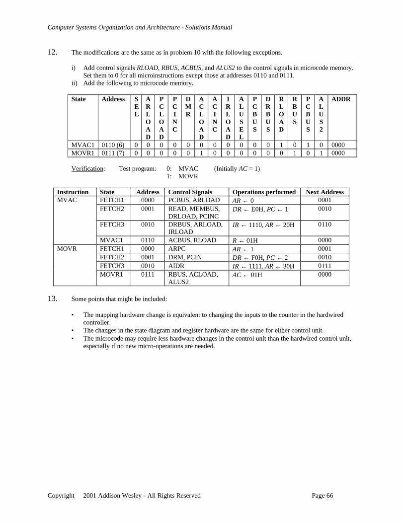
12. The modifications are the same as in problem 10 with the following exceptions.
i) Add control signals RLOAD, RBUS, ACBUS, and ALUS2 to the control signals in microcode memory.Set them to 0 for all microinstructions except those at addresses 0110 and 0111.
ii) Add the following to microcode memory.
State Address SEL
ARLOAD
PCLOAD
PCINC
DMR
ACLOAD
ACINC
IRLOAD
ALUSEL
PCBUS
DRBUS
RLOAD
RBUS
PCBUS
ALUS2
ADDR
MVAC1 0110 (6) 0 0 0 0 0 0 0 0 0 0 0 1 0 1 0 0000MOVR1 0111 (7) 0 0 0 0 0 1 0 0 0 0 0 0 1 0 1 0000
Verification: Test program: 0: MVAC (Initially AC = 1)1: MOVR
Instruction State Address Control Signals Operations performed Next AddressMVAC FETCH1 0000 PCBUS, ARLOAD AR ← 0 0001
FETCH2 0001 READ, MEMBUS,DRLOAD, PCINC
DR ← E0H, PC ← 1 0010
FETCH3 0010 DRBUS, ARLOAD,IRLOAD
IR ← 1110, AR ← 20H 0110
MVAC1 0110 ACBUS, RLOAD R ← 01H 0000MOVR FETCH1 0000 ARPC AR ← 1 0001
FETCH2 0001 DRM, PCIN DR ← F0H, PC ← 2 0010FETCH3 0010 AIDR IR ← 1111, AR ← 30H 0111MOVR1 0111 RBUS, ACLOAD,
ALUS2AC ← 01H 0000
13. Some points that might be included:
• The mapping hardware change is equivalent to changing the inputs to the counter in the hardwiredcontroller.
• The changes in the state diagram and register hardware are the same for either control unit.• The microcode may require less hardware changes in the control unit than the hardwired control unit,
especially if no new micro-operations are needed.
Computer Systems Organization and Architecture - Solutions Manual
Copyright 2001 Addison Wesley - All Rights Reserved Page 67
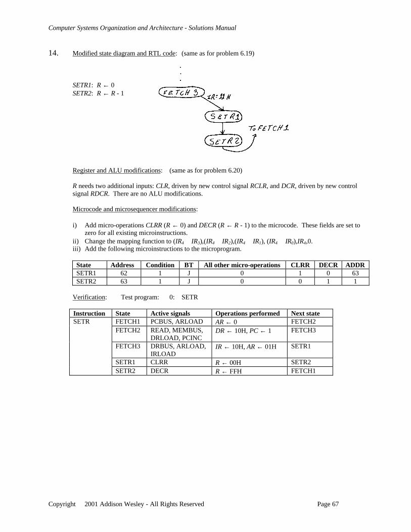
14. Modified state diagram and RTL code: (same as for problem 6.19)
SETR1: R ← 0SETR2: R ← R - 1
Register and ALU modifications: (same as for problem 6.20)
R needs two additional inputs: CLR, driven by new control signal RCLR, and DCR, driven by new controlsignal RDCR. There are no ALU modifications.
Microcode and microsequencer modifications:
i) Add micro-operations CLRR (R ← 0) and DECR (R ← R - 1) to the microcode. These fields are set tozero for all existing microinstructions.
ii) Change the mapping function to (IR4 ∨ IR3),(IR4 ∨ IR2),(IR4 ∨ IR1), (IR4 ∨ IR0),IR4,0.iii) Add the following microinstructions to the microprogram.
State Address Condition BT All other micro-operations CLRR DECR ADDRSETR1 62 1 J 0 1 0 63SETR2 63 1 J 0 0 1 1
Verification: Test program: 0: SETR
Instruction State Active signals Operations performed Next stateSETR FETCH1 PCBUS, ARLOAD AR ← 0 FETCH2
FETCH2 READ, MEMBUS,DRLOAD, PCINC
DR ← 10H, PC ← 1 FETCH3
FETCH3 DRBUS, ARLOAD,IRLOAD
IR ← 10H, AR ← 01H SETR1
SETR1 CLRR R ← 00H SETR2SETR2 DECR R ← FFH FETCH1
Computer Systems Organization and Architecture - Solutions Manual
Copyright 2001 Addison Wesley - All Rights Reserved Page 68
15. Modified state diagram and RTL code: (same as for problem 6.23)
ADDB1: AC ← AC + BSUBB1: AC ← AC - BANDB1: AC ← AC ^ BORB1: AC ← AC ∨ BXORB1: AC ← AC ⊕ B
Register and ALU modifications: (same as for problem 6.24)
i.) No ALU changes are needed!ii) Register B is added to the CPU. It sends data to the bus through tri-state buffers but does not receive
data from the bus (since it is never loaded). This is shown below.
Microcode and microsequencer modifications:
i) Add micro-operations BPLU (AC ← AC + B), BMIN (AC ← AC - B), BAND (AC ← AC ^ B),BOR (AC ← AC ∨ B), and BXOR (AC ← AC ⊕ B) to the microcode. These fields are set tozero for all existing microinstructions.
ii) Change the mapping function to IR3,IR2,IR1,IR0,0,IR4.iii) Change ALUS[1..7] such that ADD1 is replaced by ADD1 ∨ ADDB1, and so on for SUB1, AND1,
OR1, and XOR1, yielding:
ALUS1 = ADD1 ∨ ADDB1 ∨ SUB1 ∨ SUBB1 ∨ INAC1ALUS2 = SUB1 ∨ SUBB1ALUS3 = LDAC5 ∨ MOVR1 ∨ ADD1∨ ADDB1ALUS4 = SUB1 ∨ SUBB1∨ INAC1ALUS5 = XOR1 ∨ XORB1 ∨ NOT1ALUS6 = OR1 ∨ ORB1 ∨ NOT1ALUS7 = AND1 ∨ ANDB1 ∨ OR1 ∨ ORB1 ∨ XOR1 ∨ XORB1 ∨ NOT1
Computer Systems Organization and Architecture - Solutions Manual
Copyright 2001 Addison Wesley - All Rights Reserved Page 69
iv) Add the following microinstructions to the microprogram.
State Address Cond. BT All otherµµ-ops
BPLU BMIN BAND BOR BXOR ADDR
ADDB1 33 1 J 0 1 0 0 0 0 1SUBB1 37 1 J 0 0 1 0 0 0 1ANDB1 49 1 J 0 0 0 1 0 0 1ORB1 53 1 J 0 0 0 0 1 0 1XORB1 57 1 J 0 0 0 0 0 1 1
Verification: Test program shown below. Fetch cycles not shown
Instruction State Micro-operations Operations performedORB ORB1 BOR AC ← 1 ∨ 2 = 3ADDB ADDB1 BPLU AC ← 3 + 2 = 5ANDB ANDB1 BAND AC ← 5 ^ 2 = 0XORB XORB1 BXOR AC ← 0 ⊕ 2 = 2SUBB SUBB1 BMIN AC ← 2 - 2 = 0
16. PCLOAD = PCDT RBUS = ACR ∨ PLUS ∨ MINU ∨ AND ∨ OR ∨ XORTRLOAD = TRDR ALUS1 = PLUS ∨ MINU ∨ ACIN
PCBUS = ARPC ALUS2 = MINUDRHBUS = ARDT ∨ PCDT ALUS3 = ACDR ∨ ACR ∨ PLUSDRLBUS = ACDR ∨ MDR ALUS4 = MINU ∨ ACIN
ACBUS = DRAC ∨ RAC ALUS5 = XOR ∨ NOTREAD = DRM ALUS6 = OR ∨ NOT
WRITE = MDR ALUS7 = AND ∨ OR ∨ XOR ∨ NOTMEMBUSBUSMEM
= DRM = MDR
ACLOAD = ACDR ∨ ACR ∨ PLUS ∨ MINU ∨ ACIN ∨ ACZO ∨AND ∨ OR ∨ XOR ∨ NOT
17. The subroutine now consists only of its last two instructions:
State Address
Condition
BT
ARPC
ARIN
ARDT
PCIN
PCDT
DRM
DRAC
IRDR
RAC
ZALU
TRDR
ACDR
ACR
PLUS
MINU
ACIN
ACZO
AND
OR
XOR
NOT
MDR
ADDR
SUB1 61 1 J 0 0 0 1 0 1 0 0 0 0 1 0 0 0 0 0 0 0 0 0 0 0 62SUB2 62 1 R 0 0 1 0 0 0 0 0 0 0 0 0 0 0 0 0 0 0 0 0 0 0 X
Computer Systems Organization and Architecture - Solutions Manual
Copyright 2001 Addison Wesley - All Rights Reserved Page 70
18. i) The microsequencer is the same as shown in Figure 7.8, except the micro-operations fields are input todecoders which generate the micro-operations.
ii) From the microcode of Table 7.17, the following groups of micro-operations must occursimultaneously at least once, and therefore must be located in different fields:
• PCIN, DRM, and ARIN• ARPC, and IRDR• PCIN, DRM, and TRDR• ZALU, and each of the arithmetic and logic micro-operations (PLUS, MINU, ACIN, ACZO,
AND, OR, XOR, and NOT)
iii) Since some microinstructions (such as NOP1) perform no micro-operations, each field requires a NOP.
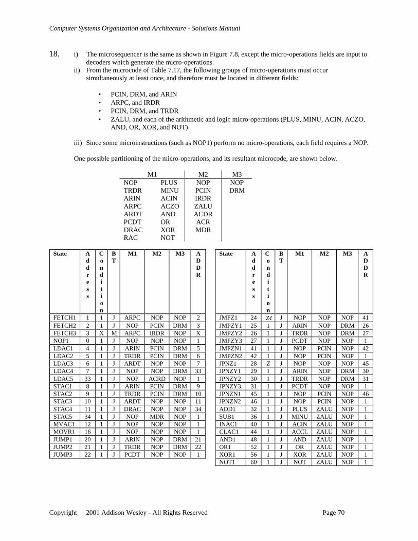
One possible partitioning of the micro-operations, and its resultant microcode, are shown below.
M1 M2 M3NOP PLUS NOP NOPTRDR MINU PCIN DRMARIN ACIN IRDRARPC ACZO ZALUARDT AND ACDRPCDT OR ACRDRAC XOR MDRRAC NOT
State Address
Condition
BT
M1 M2 M3 ADDR
State Address
Condition
BT
M1 M2 M3 ADDR
FETCH1 1 1 J ARPC NOP NOP 2 JMPZ1 24 Z′ J NOP NOP NOP 41FETCH2 2 1 J NOP PCIN DRM 3 JMPZY1 25 1 J ARIN NOP DRM 26FETCH3 3 X M ARPC IRDR NOP X JMPZY2 26 1 J TRDR NOP DRM 27NOP1 0 1 J NOP NOP NOP 1 JMPZY3 27 1 J PCDT NOP NOP 1LDAC1 4 1 J ARIN PCIN DRM 5 JMPZN1 41 1 J NOP PCIN NOP 42LDAC2 5 1 J TRDR PCIN DRM 6 JMPZN2 42 1 J NOP PCIN NOP 1LDAC3 6 1 J ARDT NOP NOP 7 JPNZ1 28 Z J NOP NOP NOP 45LDAC4 7 1 J NOP NOP DRM 33 JPNZY1 29 1 J ARIN NOP DRM 30LDAC5 33 1 J NOP ACRD NOP 1 JPNZY2 30 1 J TRDR NOP DRM 31STAC1 8 1 J ARIN PCIN DRM 9 JPNZY3 31 1 J PCDT NOP NOP 1STAC2 9 1 J TRDR PCIN DRM 10 JPNZN1 45 1 J NOP PCIN NOP 46STAC3 10 1 J ARDT NOP NOP 11 JPNZN2 46 1 J NOP PCIN NOP 1STAC4 11 1 J DRAC NOP NOP 34 ADD1 32 1 J PLUS ZALU NOP 1STAC5 34 1 J NOP MDR NOP 1 SUB1 36 1 J MINU ZALU NOP 1MVAC1 12 1 J NOP NOP NOP 1 INAC1 40 1 J ACIN ZALU NOP 1MOVR1 16 1 J NOP NOP NOP 1 CLAC1 44 1 J ACCL ZALU NOP 1JUMP1 20 1 J ARIN NOP DRM 21 AND1 48 1 J AND ZALU NOP 1JUMP2 21 1 J TRDR NOP DRM 22 OR1 52 1 J OR ZALU NOP 1JUMP3 22 1 J PCDT NOP NOP 1 XOR1 56 1 J XOR ZALU NOP 1
NOT1 60 1 J NOT ZALU NOP 1
Computer Systems Organization and Architecture - Solutions Manual
Copyright 2001 Addison Wesley - All Rights Reserved Page 71
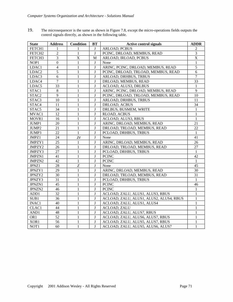
19. The microsequencer is the same as shown in Figure 7.8, except the micro-operations fields outputs thecontrol signals directly, as shown in the following table.
State Address Condition BT Active control signals ADDRFETCH1 1 1 J ARLOAD, PCBUS 2FETCH2 2 1 J PCINC, DRLOAD, MEMBUS, READ 3FETCH3 3 X M ARLOAD, IRLOAD, PCBUS XNOP1 0 1 J None 1LDAC1 4 1 J ARINC, PCINC, DRLOAD, MEMBUS, READ 5LDAC2 5 1 J PCINC, DRLOAD, TRLOAD, MEMBUS, READ 6LDAC3 6 1 J ARLOAD, DRHBUS, TRBUS 7LDAC4 7 1 J DRLOAD, MEMBUS, READ 33LDAC5 33 1 J ACLOAD, ALUS3, DRLBUS 1STAC1 8 1 J ARINC, PCINC, DRLOAD, MEMBUS, READ 9STAC2 9 1 J PCINC, DRLOAD, TRLOAD, MEMBUS, READ 10STAC3 10 1 J ARLOAD, DRHBUS, TRBUS 11STAC4 11 1 J DRLOAD, ACBUS 34STAC5 34 1 J DRLBUS, BUSMEM, WRITE 1MVAC1 12 1 J RLOAD, ACBUS 1MOVR1 16 1 J ACLOAD, ALUS3, RBUS 1JUMP1 20 1 J ARINC, DRLOAD, MEMBUS, READ 21JUMP2 21 1 J DRLOAD, TRLOAD, MEMBUS, READ 22JUMP3 22 1 J PCLOAD, DRHBUS, TRBUS 1JMPZ1 24 Z′ J None 41JMPZY1 25 1 J ARINC, DRLOAD, MEMBUS, READ 26JMPZY2 26 1 J DRLOAD, TRLOAD, MEMBUS, READ 27JMPZY3 27 1 J PCLOAD, DRHBUS, TRBUS 1JMPZN1 41 1 J PCINC 42JMPZN2 42 1 J PCINC 1JPNZ1 28 Z J None 45JPNZY1 29 1 J ARINC, DRLOAD, MEMBUS, READ 30JPNZY2 30 1 J DRLOAD, TRLOAD, MEMBUS, READ 31JPNZY3 31 1 J PCLOAD, DRHBUS, TRBUS 1JPNZN1 45 1 J PCINC 46JPNZN2 46 1 J PCINC 1ADD1 32 1 J ACLOAD, ZALU, ALUS1, ALUS3, RBUS 1SUB1 36 1 J ACLOAD, ZALU, ALUS1, ALUS2, ALUS4, RBUS 1INAC1 40 1 J ACLOAD, ZALU, ALUS1, ALUS4 1CLAC1 44 1 J ACLOAD, ZALU 1AND1 48 1 J ACLOAD, ZALU, ALUS7, RBUS 1OR1 52 1 J ACLOAD, ZALU, ALUS6, ALUS7, RBUS 1XOR1 56 1 J ACLOAD, ZALU, ALUS5, ALUS7, RBUS 1NOT1 60 1 J ACLOAD, ZALU, ALUS5, ALUS6, ALUS7 1
Computer Systems Organization and Architecture - Solutions Manual
Copyright 2001 Addison Wesley - All Rights Reserved Page 72
20. This solution is the same as for Problem 6.18. The student can execute the following program using theRelatively Simple CPU simulator to verify that each instruction performs properly.
0: LDAC 0000 (AC ← 1)NOPMVAC (R ← 1)ADD (AC ← 2, Z ← 0)INAC (AC ← 3, Z ← 0)XOR (AC ← 2, Z ← 0)AND (AC ← 0, Z ← 1)
9: JMPZ 000D (jump is taken)NOP (skipped by JMPZ 000D)
D: JPNZ 0009 (jump is not taken)NOT (AC ← FF, Z ← 0)JMPZ 0009 (jump is not taken)JPNZ 0018 (jump is taken)NOP (skipped by JMPZ 0018)
18: CLAC (AC ← 0, Z ← 1)OR (AC ← 1, Z ← 0)SUB (AC ← 0, Z ← 1)MOVR (AC ← 1)STAC 0030 (M[30] ← 1)AND (AC ← 1, Z ← 0)JUMP 0000 (start again)
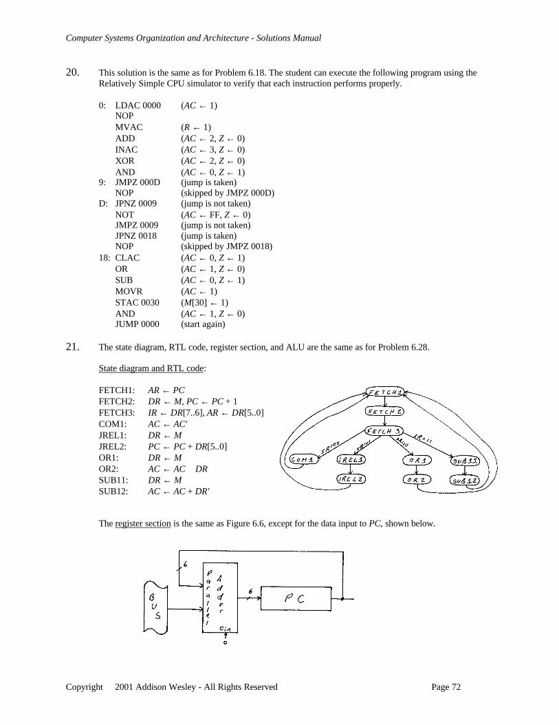
21. The state diagram, RTL code, register section, and ALU are the same as for Problem 6.28.
State diagram and RTL code:
FETCH1: AR ← PCFETCH2: DR ← M, PC ← PC + 1FETCH3: IR ← DR[7..6], AR ← DR[5..0]COM1: AC ← AC'JREL1: DR ← MJREL2: PC ← PC + DR[5..0]OR1: DR ← MOR2: AC ← AC ∨ DRSUB11: DR ← MSUB12: AC ← AC + DR'
The register section is the same as Figure 6.6, except for the data input to PC, shown below.
Computer Systems Organization and Architecture - Solutions Manual
Copyright 2001 Addison Wesley - All Rights Reserved Page 73
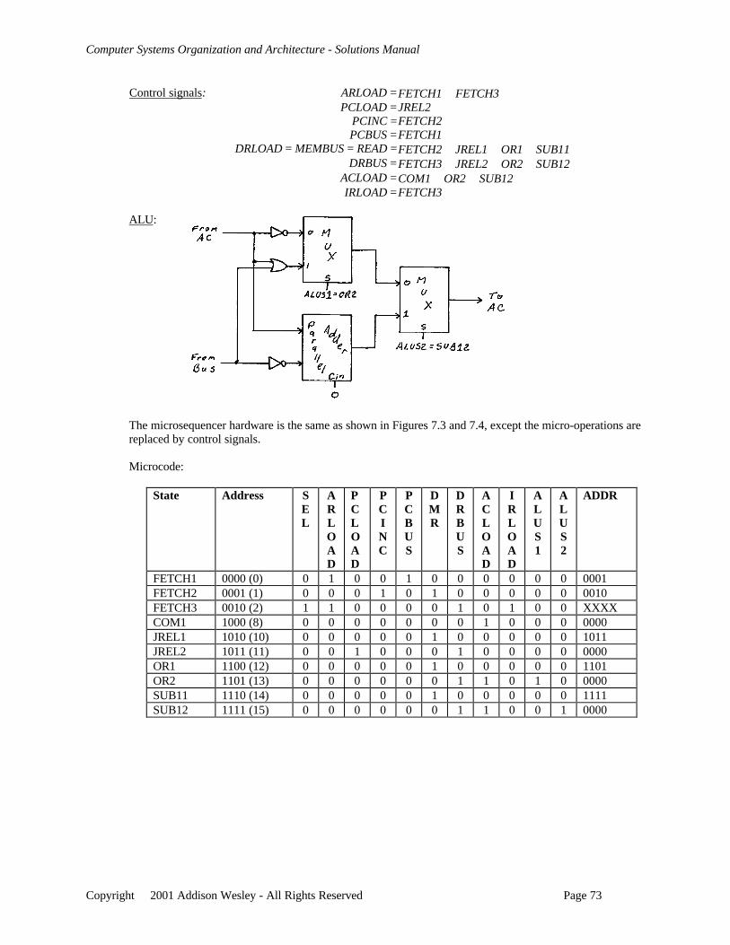
Control signals: ARLOAD =FETCH1 ∨ FETCH3PCLOAD =JREL2
PCINC =FETCH2PCBUS =FETCH1
DRLOAD = MEMBUS = READ =FETCH2 ∨ JREL1∨ OR1∨ SUB11DRBUS =FETCH3 ∨ JREL2 ∨ OR2 ∨ SUB12
ACLOAD =COM1 ∨ OR2 ∨ SUB12IRLOAD =FETCH3
ALU:
The microsequencer hardware is the same as shown in Figures 7.3 and 7.4, except the micro-operations arereplaced by control signals.
Microcode:
State Address SEL
ARLOAD
PCLOAD
PCINC
PCBUS
DMR
DRBUS
ACLOAD
IRLOAD
ALUS1
ALUS2
ADDR
FETCH1 0000 (0) 0 1 0 0 1 0 0 0 0 0 0 0001FETCH2 0001 (1) 0 0 0 1 0 1 0 0 0 0 0 0010FETCH3 0010 (2) 1 1 0 0 0 0 1 0 1 0 0 XXXXCOM1 1000 (8) 0 0 0 0 0 0 0 1 0 0 0 0000JREL1 1010 (10) 0 0 0 0 0 1 0 0 0 0 0 1011JREL2 1011 (11) 0 0 1 0 0 0 1 0 0 0 0 0000OR1 1100 (12) 0 0 0 0 0 1 0 0 0 0 0 1101OR2 1101 (13) 0 0 0 0 0 0 1 1 0 1 0 0000SUB11 1110 (14) 0 0 0 0 0 1 0 0 0 0 0 1111SUB12 1111 (15) 0 0 0 0 0 0 1 1 0 0 1 0000
Computer Systems Organization and Architecture - Solutions Manual
Copyright 2001 Addison Wesley - All Rights Reserved Page 74
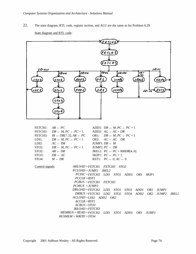
22. The state diagram, RTL code, register section, and ALU are the same as for Problem 6.29.
State diagram and RTL code:
FETCH1: AR ← PC ADD1: DR ← M, PC ← PC + 1FETCH2: DR ← M, PC ← PC + 1 ADD2: AC ← AC + DRFETCH3: IR ← DR[7..5], AR ← PC OR1: DR ← M, PC ← PC + 1LDI1: DR ← M, PC ← PC + 1 OR2: AC ← AC ∨ DRLDI2: AC ← DR JUMP1: DR ← MSTO1: DR ← M, PC ← PC + 1 JUMP2: PC ← DRSTO2: AR ← DR JREL1: PC ← PC + 000DR[4..0]STO3: DR ← AC SKIP1: PC ← PC + 1STO4: M ← DR RST1: PC ← 0, AC ← 0
Control signals: ARLOAD =FETCH1 ∨ FETCH3 ∨ STO2PCLOAD =JUMP2 ∨ JREL2
PCINC =FETCH2 ∨ LDI1 ∨ STO1 ∨ ADD1 ∨ OR1 ∨ SKIP1PCCLR =RST1
PCBUS =FETCH1 ∨ FETCH3PCMUX =JUMP2DRLOAD =FETCH2 ∨ LDI1 ∨ STO1 ∨ STO3 ∨ ADD1 ∨ OR1 ∨ JUMP1
DRBUS =FETCH3 ∨ LDI2 ∨ STO2 ∨ STO4 ∨ ADD2 ∨ OR2 ∨ JUMP2 ∨ JREL1ACLOAD =LDI2 ∨ ADD2 ∨ OR2
ACCLR =RST1ACBUS =STO3
IRLOAD =FETCH3MEMBUS = READ =FETCH2 ∨ LDI1 ∨ STO1 ∨ ADD1 ∨ OR1 ∨ JUMP1
BUSMEM = WRITE =STO4
Computer Systems Organization and Architecture - Solutions Manual
Copyright 2001 Addison Wesley - All Rights Reserved Page 75
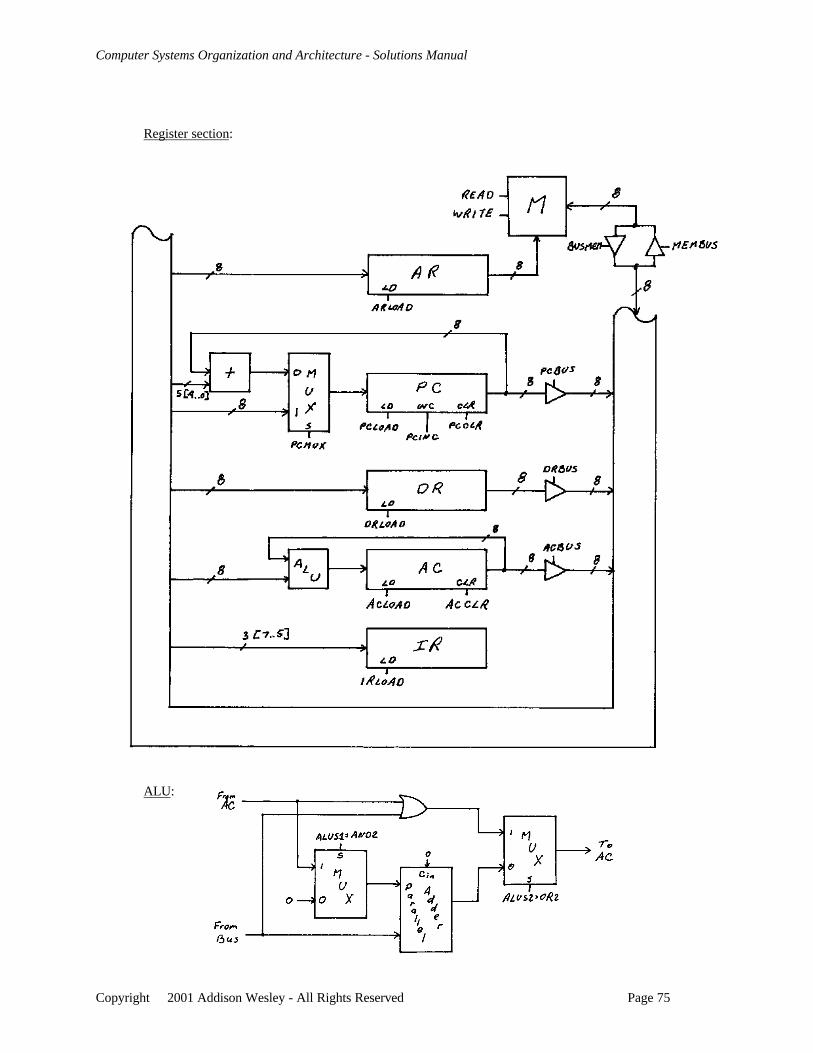
Register section:
ALU:
Computer Systems Organization and Architecture - Solutions Manual
Copyright 2001 Addison Wesley - All Rights Reserved Page 76
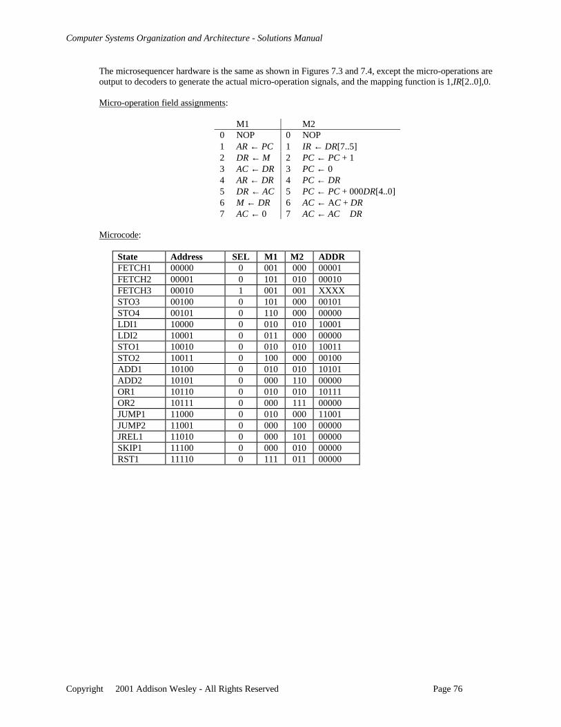
The microsequencer hardware is the same as shown in Figures 7.3 and 7.4, except the micro-operations areoutput to decoders to generate the actual micro-operation signals, and the mapping function is 1,IR[2..0],0.
Micro-operation field assignments:
M1 M20 NOP 0 NOP1 AR ← PC 1 IR ← DR[7..5]2 DR ← M 2 PC ← PC + 13 AC ← DR 3 PC ← 04 AR ← DR 4 PC ← DR5 DR ← AC 5 PC ← PC + 000DR[4..0]6 M ← DR 6 AC ← AC + DR7 AC ← 0 7 AC ← AC ∨ DR
Microcode:
State Address SEL M1 M2 ADDRFETCH1 00000 0 001 000 00001FETCH2 00001 0 101 010 00010FETCH3 00010 1 001 001 XXXXSTO3 00100 0 101 000 00101STO4 00101 0 110 000 00000LDI1 10000 0 010 010 10001LDI2 10001 0 011 000 00000STO1 10010 0 010 010 10011STO2 10011 0 100 000 00100ADD1 10100 0 010 010 10101ADD2 10101 0 000 110 00000OR1 10110 0 010 010 10111OR2 10111 0 000 111 00000JUMP1 11000 0 010 000 11001JUMP2 11001 0 000 100 00000JREL1 11010 0 000 101 00000SKIP1 11100 0 000 010 00000RST1 11110 0 111 011 00000
Computer Systems Organization and Architecture - Solutions Manual
Copyright 2001 Addison Wesley - All Rights Reserved Page 77
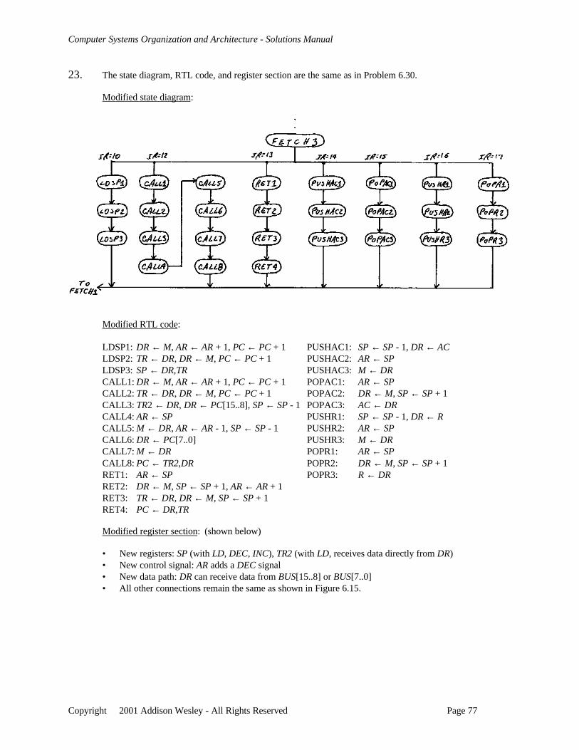
23. The state diagram, RTL code, and register section are the same as in Problem 6.30.
Modified state diagram:
Modified RTL code:
LDSP1: DR ← M, AR ← AR + 1, PC ← PC + 1 PUSHAC1: SP ← SP - 1, DR ← ACLDSP2: TR ← DR, DR ← M, PC ← PC + 1 PUSHAC2: AR ← SPLDSP3: SP ← DR,TR PUSHAC3: M ← DRCALL1: DR ← M, AR ← AR + 1, PC ← PC + 1 POPAC1: AR ← SPCALL2: TR ← DR, DR ← M, PC ← PC + 1 POPAC2: DR ← M, SP ← SP + 1CALL3: TR2 ← DR, DR ← PC[15..8], SP ← SP - 1 POPAC3: AC ← DRCALL4: AR ← SP PUSHR1: SP ← SP - 1, DR ← RCALL5: M ← DR, AR ← AR - 1, SP ← SP - 1 PUSHR2: AR ← SPCALL6: DR ← PC[7..0] PUSHR3: M ← DRCALL7: M ← DR POPR1: AR ← SPCALL8: PC ← TR2,DR POPR2: DR ← M, SP ← SP + 1RET1: AR ← SP POPR3: R ← DRRET2: DR ← M, SP ← SP + 1, AR ← AR + 1RET3: TR ← DR, DR ← M, SP ← SP + 1RET4: PC ← DR,TR
Modified register section: (shown below)
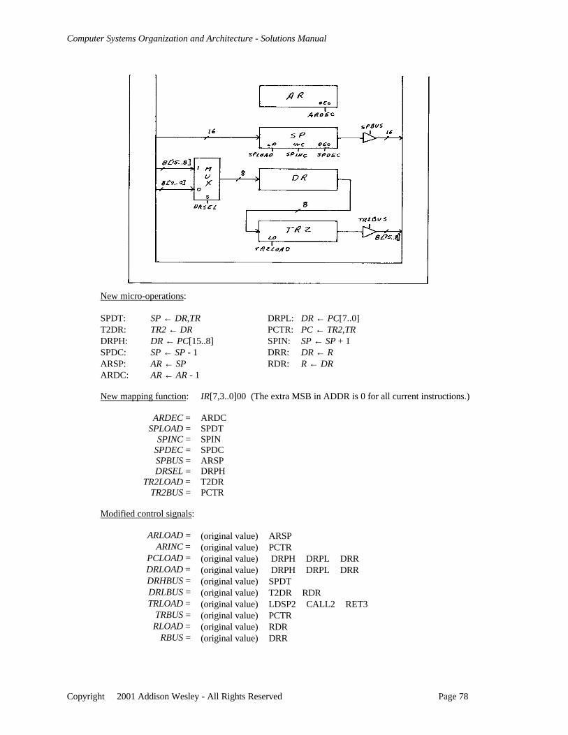
• New registers: SP (with LD, DEC, INC), TR2 (with LD, receives data directly from DR)• New control signal: AR adds a DEC signal• New data path: DR can receive data from BUS[15..8] or BUS[7..0]• All other connections remain the same as shown in Figure 6.15.
Computer Systems Organization and Architecture - Solutions Manual
Copyright 2001 Addison Wesley - All Rights Reserved Page 78
New micro-operations:
SPDT: SP ← DR,TR DRPL: DR ← PC[7..0]T2DR: TR2 ← DR PCTR: PC ← TR2,TRDRPH: DR ← PC[15..8] SPIN: SP ← SP + 1SPDC: SP ← SP - 1 DRR: DR ← RARSP: AR ← SP RDR: R ← DRARDC: AR ← AR - 1
New mapping function: IR[7,3..0]00 (The extra MSB in ADDR is 0 for all current instructions.)
ARDEC = ARDCSPLOAD = SPDT
SPINC = SPINSPDEC = SPDCSPBUS = ARSPDRSEL = DRPH
TR2LOAD = T2DRTR2BUS = PCTR
Modified control signals:
ARLOAD = (original value) ∨ ARSPARINC = (original value) ∨ PCTR
PCLOAD = (original value) ∨ DRPH ∨ DRPL ∨ DRRDRLOAD = (original value) ∨ DRPH ∨ DRPL ∨ DRRDRHBUS = (original value) ∨ SPDTDRLBUS = (original value) ∨ T2DR ∨ RDRTRLOAD = (original value) ∨ LDSP2 ∨ CALL2 ∨ RET3
TRBUS = (original value) ∨ PCTRRLOAD = (original value) ∨ RDR
RBUS = (original value) ∨ DRR
Computer Systems Organization and Architecture - Solutions Manual
Copyright 2001 Addison Wesley - All Rights Reserved Page 79
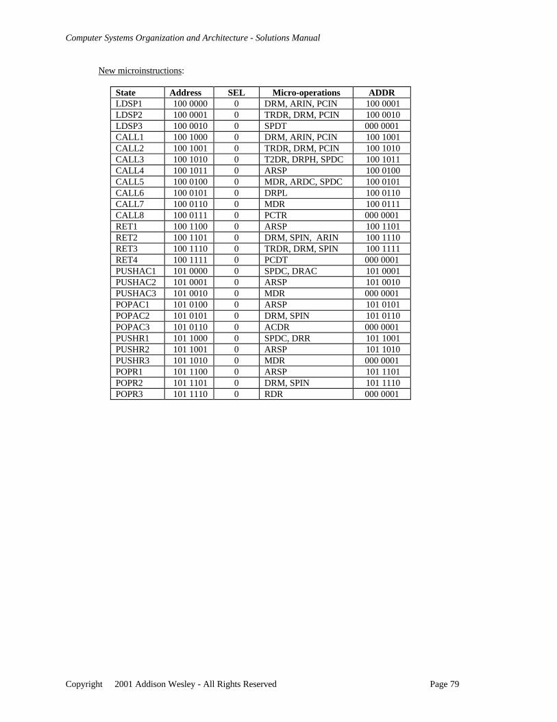
New microinstructions:
State Address SEL Micro-operations ADDRLDSP1 100 0000 0 DRM, ARIN, PCIN 100 0001LDSP2 100 0001 0 TRDR, DRM, PCIN 100 0010LDSP3 100 0010 0 SPDT 000 0001CALL1 100 1000 0 DRM, ARIN, PCIN 100 1001CALL2 100 1001 0 TRDR, DRM, PCIN 100 1010CALL3 100 1010 0 T2DR, DRPH, SPDC 100 1011CALL4 100 1011 0 ARSP 100 0100CALL5 100 0100 0 MDR, ARDC, SPDC 100 0101CALL6 100 0101 0 DRPL 100 0110CALL7 100 0110 0 MDR 100 0111CALL8 100 0111 0 PCTR 000 0001RET1 100 1100 0 ARSP 100 1101RET2 100 1101 0 DRM, SPIN, ARIN 100 1110RET3 100 1110 0 TRDR, DRM, SPIN 100 1111RET4 100 1111 0 PCDT 000 0001PUSHAC1 101 0000 0 SPDC, DRAC 101 0001PUSHAC2 101 0001 0 ARSP 101 0010PUSHAC3 101 0010 0 MDR 000 0001POPAC1 101 0100 0 ARSP 101 0101POPAC2 101 0101 0 DRM, SPIN 101 0110POPAC3 101 0110 0 ACDR 000 0001PUSHR1 101 1000 0 SPDC, DRR 101 1001PUSHR2 101 1001 0 ARSP 101 1010PUSHR3 101 1010 0 MDR 000 0001POPR1 101 1100 0 ARSP 101 1101POPR2 101 1101 0 DRM, SPIN 101 1110POPR3 101 1110 0 RDR 000 0001
Computer Systems Organization and Architecture - Solutions Manual
Copyright 2001 Addison Wesley - All Rights Reserved Page 80
Chapter 8
1. a) 64 = 01000000 64' = 1100 0000
b) 33 = 0010 0001 33' = 1101 1111
c) -1 = 1111 1111 -1' = 0000 0001
2. Non-negative Unsigned two's-complement
a) 29 = 0001 1101 0001 1101
b) -128 = N/A 1000 0000
c) 199 = 1100 0111 N/A
3. Signed-Magnitude Signed-Two's Complement
a) -63 = 1011 1111 1100 0001
b) 147 = N/A N/A
c) 85 = 0101 0101 0101 0101
4. a) 0011 1101 (180 - 119 = 61)
b) N/A (56 + 205 = 261, overflow)
c) 1111 1111 (139 + 116 = 255)
d) N/A (116 - 139 = -23, negative number)
5. a) N/A (-76 - 119 = -193, overflow)
b) 0000 0101 (56 + -51 = 5)
c) 1111 1111 (-117 + 116 = -1)
d) N/A (116 - -117 = 233, overflow)
6. The worst cases are +127 + (-1) = +126 and +0 + (-128) = -128, both of which produce valid results.
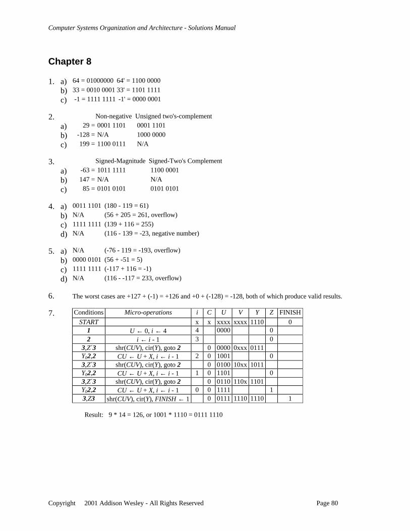
7. Conditions Micro-operations i C U V Y Z FINISH
START x x xxxx xxxx 1110 01 U ← 0, i ← 4 4 0000 02 i ← i - 1 3 0
3,Z´3 shr(CUV), cir(Y), goto 2 0 0000 0xxx 0111Y02,2 CU ← U + X, i ← i - 1 2 0 1001 03,Z´3 shr(CUV), cir(Y), goto 2 0 0100 10xx 1011Y02,2 CU ← U + X, i ← i - 1 1 0 1101 03,Z´3 shr(CUV), cir(Y), goto 2 0 0110 110x 1101Y02,2 CU ← U + X, i ← i - 1 0 0 1111 13,Z3 shr(CUV), cir(Y), FINISH ← 1 0 0111 1110 1110 1
Result: 9 * 14 = 126, or 1001 * 1110 = 0111 1110
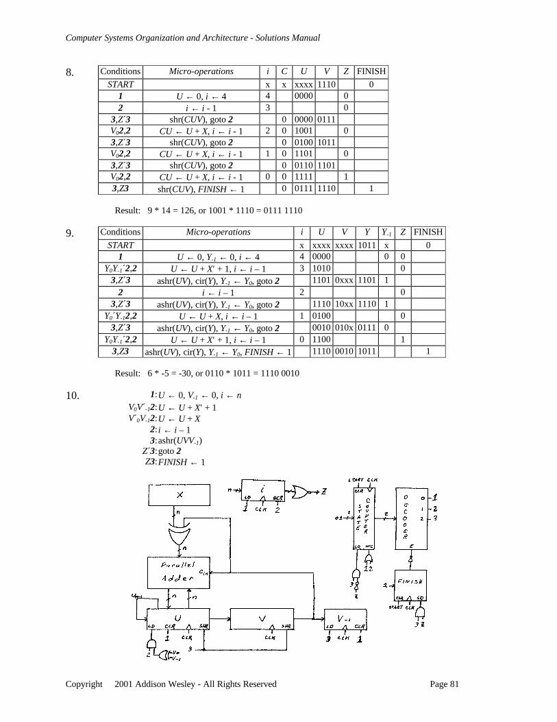
Computer Systems Organization and Architecture - Solutions Manual
Copyright 2001 Addison Wesley - All Rights Reserved Page 81
8. Conditions Micro-operations i C U V Z FINISH
START x x xxxx 1110 01 U ← 0, i ← 4 4 0000 02 i ← i - 1 3 0
3,Z´3 shr(CUV), goto 2 0 0000 0111V02,2 CU ← U + X, i ← i - 1 2 0 1001 03,Z´3 shr(CUV), goto 2 0 0100 1011V02,2 CU ← U + X, i ← i - 1 1 0 1101 03,Z´3 shr(CUV), goto 2 0 0110 1101V02,2 CU ← U + X, i ← i - 1 0 0 1111 13,Z3 shr(CUV), FINISH ← 1 0 0111 1110 1
Result: 9 * 14 = 126, or 1001 * 1110 = 0111 1110
9. Conditions Micro-operations i U V Y Y-1 Z FINISH
START x xxxx xxxx 1011 x 01 U ← 0, Y-1 ← 0, i ← 4 4 0000 0 0
Y0Y-1´2,2 U ← U + X′ + 1, i ← i – 1 3 1010 03,Z´3 ashr(UV), cir(Y), Y-1 ← Y0, goto 2 1101 0xxx 1101 1
2 i ← i – 1 2 03,Z´3 ashr(UV), cir(Y), Y-1 ← Y0, goto 2 1110 10xx 1110 1
Y0´Y-12,2 U ← U + X, i ← i – 1 1 0100 03,Z´3 ashr(UV), cir(Y), Y-1 ← Y0, goto 2 0010 010x 0111 0
Y0Y-1´2,2 U ← U + X′ + 1, i ← i – 1 0 1100 13,Z3 ashr(UV), cir(Y), Y-1 ← Y0, FINISH ← 1 1110 0010 1011 1
Result: 6 * -5 = -30, or 0110 * 1011 = 1110 0010
10. 1:U ← 0, V-1 ← 0, i ← nV0V´-12:U ← U + X′ + 1V´0V-12:U ← U + X
2:i ← i – 13:ashr(UVV-1)
Z´3:goto 2Z3:FINISH ← 1
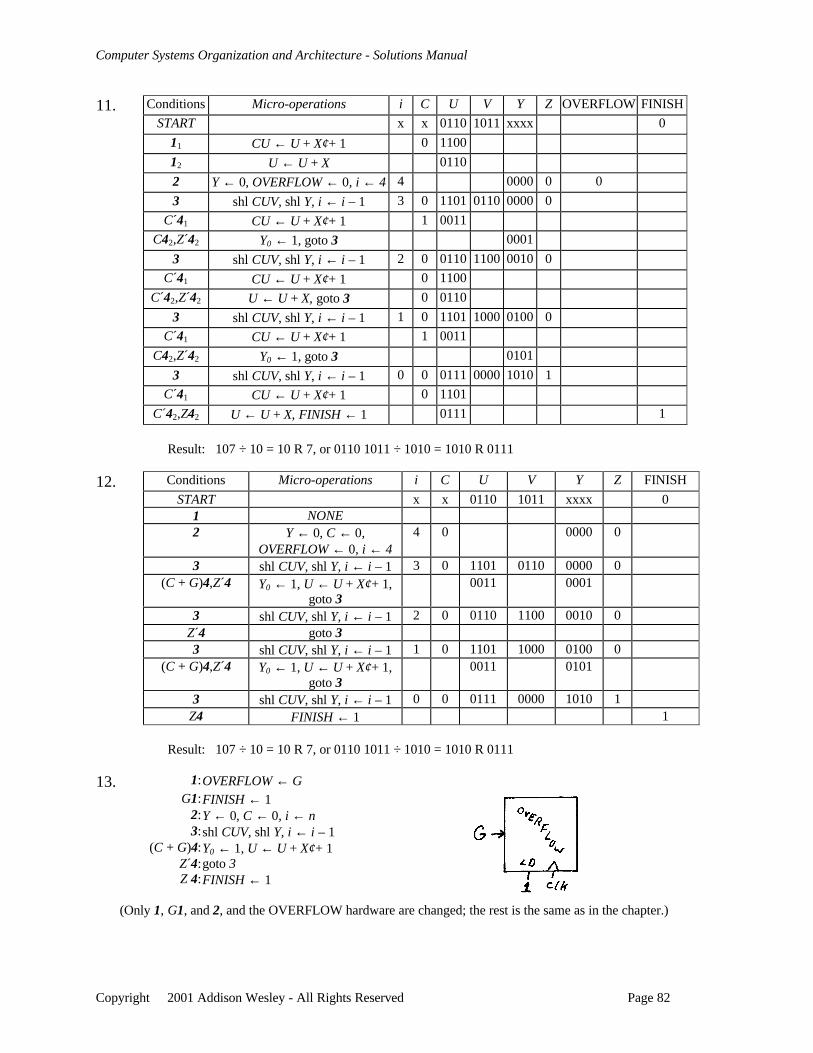
Computer Systems Organization and Architecture - Solutions Manual
Copyright 2001 Addison Wesley - All Rights Reserved Page 82
11. Conditions Micro-operations i C U V Y Z OVERFLOW FINISH
START x x 0110 1011 xxxx 0
11 CU ← U + X′ + 1 0 1100
12 U ← U + X 0110
2 Y ← 0, OVERFLOW ← 0, i ← 4 4 0000 0 0
3 shl CUV, shl Y, i ← i – 1 3 0 1101 0110 0000 0
C´41 CU ← U + X′ + 1 1 0011
C42,Z´42 Y0 ← 1, goto 3 0001
3 shl CUV, shl Y, i ← i – 1 2 0 0110 1100 0010 0
C´41 CU ← U + X′ + 1 0 1100
C´42,Z´42 U ← U + X, goto 3 0 0110
3 shl CUV, shl Y, i ← i – 1 1 0 1101 1000 0100 0
C´41 CU ← U + X′ + 1 1 0011
C42,Z´42 Y0 ← 1, goto 3 0101
3 shl CUV, shl Y, i ← i – 1 0 0 0111 0000 1010 1
C´41 CU ← U + X′ + 1 0 1101
C´42,Z42 U ← U + X, FINISH ← 1 0111 1
Result: 107 ÷ 10 = 10 R 7, or 0110 1011 ÷ 1010 = 1010 R 0111
12. Conditions Micro-operations i C U V Y Z FINISH
START x x 0110 1011 xxxx 01 NONE2 Y ← 0, C ← 0,
OVERFLOW ← 0, i ← 44 0 0000 0
3 shl CUV, shl Y, i ← i – 1 3 0 1101 0110 0000 0(C + G)4,Z´4 Y0 ← 1, U ← U + X′ + 1,
goto 30011 0001
3 shl CUV, shl Y, i ← i – 1 2 0 0110 1100 0010 0Z´4 goto 33 shl CUV, shl Y, i ← i – 1 1 0 1101 1000 0100 0
(C + G)4,Z´4 Y0 ← 1, U ← U + X′ + 1,goto 3
0011 0101
3 shl CUV, shl Y, i ← i – 1 0 0 0111 0000 1010 1Z4 FINISH ← 1 1
Result: 107 ÷ 10 = 10 R 7, or 0110 1011 ÷ 1010 = 1010 R 0111
13. 1:OVERFLOW ← GG1:FINISH ← 1
2:Y ← 0, C ← 0, i ← n3:shl CUV, shl Y, i ← i – 1
(C + G)4:Y0 ← 1, U ← U + X′ + 1Z´4:goto 3Z 4:FINISH ← 1
(Only 1, G1, and 2, and the OVERFLOW hardware are changed; the rest is the same as in the chapter.)
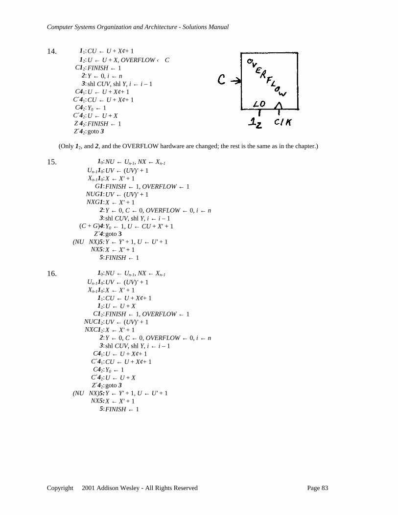
Computer Systems Organization and Architecture - Solutions Manual
Copyright 2001 Addison Wesley - All Rights Reserved Page 83
14. 11:CU ← U + X′ + 112:U ← U + X, OVERFLOW ← C
C12:FINISH ← 12:Y ← 0, i ← n3: shl CUV, shl Y, i ← i – 1
C41:U ← U + X′ + 1C´41:CU ← U + X′ + 1C42:Y0 ← 1
C´42:U ← U + XZ 42:FINISH ← 1Z´42:goto 3
(Only 12, and 2, and the OVERFLOW hardware are changed; the rest is the same as in the chapter.)
15. 10:NU ← Un-1, NX ← Xn-1
Un-110:UV ← (UV)' + 1Xn-110:X ← X' + 1
G1:FINISH ← 1, OVERFLOW ← 1NUG1:UV ← (UV)' + 1NXG1:X ← X' + 1
2:Y ← 0, C ← 0, OVERFLOW ← 0, i ← n3:shl CUV, shl Y, i ← i – 1
(C + G)4:Y0 ← 1, U ← CU + X′ + 1Z´4:goto 3
(NU⊕NX)5:Y ← Y' + 1, U ← U' + 1NX5:X ← X' + 1
5:FINISH ← 1
16. 10:NU ← Un-1, NX ← Xn-1
Un-110:UV ← (UV)' + 1Xn-110:X ← X' + 1
11:CU ← U + X′ + 112:U ← U + X
C12:FINISH ← 1, OVERFLOW ← 1NUC12:UV ← (UV)' + 1NXC12:X ← X' + 1
2:Y ← 0, C ← 0, OVERFLOW ← 0, i ← n3:shl CUV, shl Y, i ← i – 1
C41:U ← U + X′ + 1C´41:CU ← U + X′ + 1C42:Y0 ← 1
C´42:U ← U + XZ´42:goto 3
(NU⊕NX)5:Y ← Y' + 1, U ← U' + 1NX5:X ← X' + 1
5:FINISH ← 1
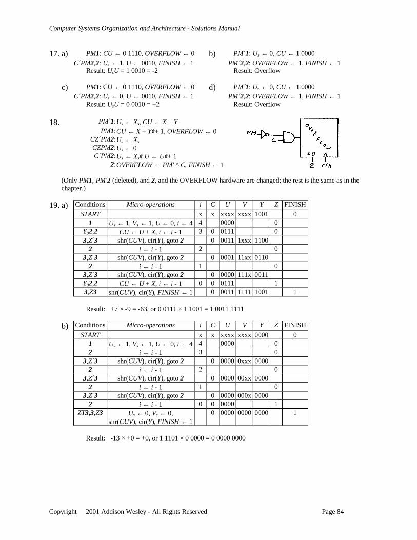
Computer Systems Organization and Architecture - Solutions Manual
Copyright 2001 Addison Wesley - All Rights Reserved Page 84
17. a) PM1: CU ← 0 1110, OVERFLOW ← 0 b) PM´1: Us ← 0, CU ← 1 0000C´PM2,2: Us ← 1, U ← 0010, FINISH ← 1 PM´2,2: OVERFLOW ← 1, FINISH ← 1
Result: UsU = 1 0010 = -2 Result: Overflow
c) PM1: CU ← 0 1110, OVERFLOW ← 0 d) PM´1: Us ← 0, CU ← 1 0000C´PM2,2: Us ← 0, U ← 0010, FINISH ← 1 PM´2,2: OVERFLOW ← 1, FINISH ← 1
Result: UsU = 0 0010 = +2 Result: Overflow
18. PM´1:Us ← Xs, CU ← X + YPM1:CU ← X + Y′ + 1, OVERFLOW ← 0
CZ´PM2:Us ← Xs
CZPM2:Us ← 0C´PM2:Us ← Xs′, U ← U′ + 1
2:OVERFLOW ← PM' ^ C, FINISH ← 1
(Only PM1, PM'2 (deleted), and 2, and the OVERFLOW hardware are changed; the rest is the same as in thechapter.)
19. a) Conditions Micro-operations i C U V Y Z FINISH
START x x xxxx xxxx 1001 01 Us ← 1, Vs ← 1, U ← 0, i ← 4 4 0000 0
Y02,2 CU ← U + X, i ← i - 1 3 0 0111 03,Z´3 shr(CUV), cir(Y), goto 2 0 0011 1xxx 1100
2 i ← i - 1 2 03,Z´3 shr(CUV), cir(Y), goto 2 0 0001 11xx 0110
2 i ← i - 1 1 03,Z´3 shr(CUV), cir(Y), goto 2 0 0000 111x 0011Y02,2 CU ← U + X, i ← i - 1 0 0 0111 13,Z3 shr(CUV), cir(Y), FINISH ← 1 0 0011 1111 1001 1
Result: +7 × -9 = -63, or 0 0111 × 1 1001 = 1 0011 1111
b) Conditions Micro-operations i C U V Y Z FINISH
START x x xxxx xxxx 0000 01 Us ← 1, Vs ← 1, U ← 0, i ← 4 4 0000 02 i ← i - 1 3 0
3,Z´3 shr(CUV), cir(Y), goto 2 0 0000 0xxx 00002 i ← i - 1 2 0
3,Z´3 shr(CUV), cir(Y), goto 2 0 0000 00xx 00002 i ← i - 1 1 0
3,Z´3 shr(CUV), cir(Y), goto 2 0 0000 000x 00002 i ← i - 1 0 0 0000 1
ZT3,3,Z3 Us ← 0, Vs ← 0,shr(CUV), cir(Y), FINISH ← 1
0 0000 0000 0000 1
Result: -13 × +0 = +0, or 1 1101 × 0 0000 = 0 0000 0000
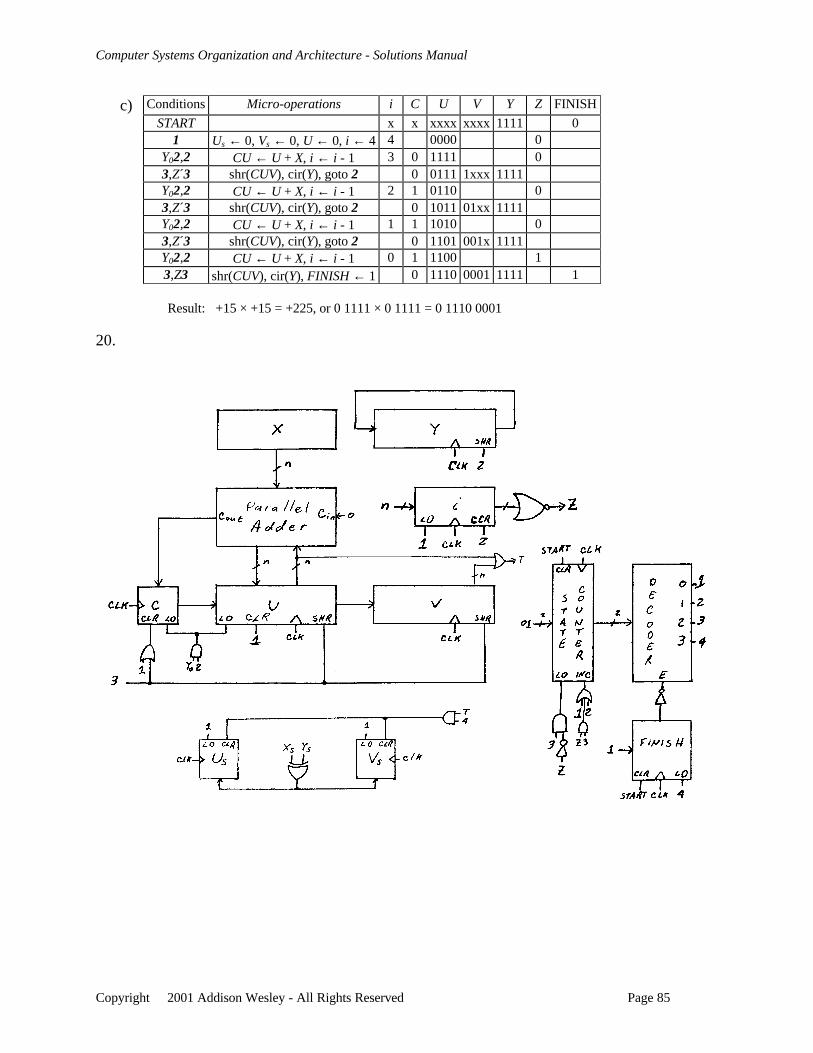
Computer Systems Organization and Architecture - Solutions Manual
Copyright 2001 Addison Wesley - All Rights Reserved Page 85
c) Conditions Micro-operations i C U V Y Z FINISH
START x x xxxx xxxx 1111 01 Us ← 0, Vs ← 0, U ← 0, i ← 4 4 0000 0
Y02,2 CU ← U + X, i ← i - 1 3 0 1111 03,Z´3 shr(CUV), cir(Y), goto 2 0 0111 1xxx 1111Y02,2 CU ← U + X, i ← i - 1 2 1 0110 03,Z´3 shr(CUV), cir(Y), goto 2 0 1011 01xx 1111Y02,2 CU ← U + X, i ← i - 1 1 1 1010 03,Z´3 shr(CUV), cir(Y), goto 2 0 1101 001x 1111Y02,2 CU ← U + X, i ← i - 1 0 1 1100 13,Z3 shr(CUV), cir(Y), FINISH ← 1 0 1110 0001 1111 1
Result: +15 × +15 = +225, or 0 1111 × 0 1111 = 0 1110 0001
20.
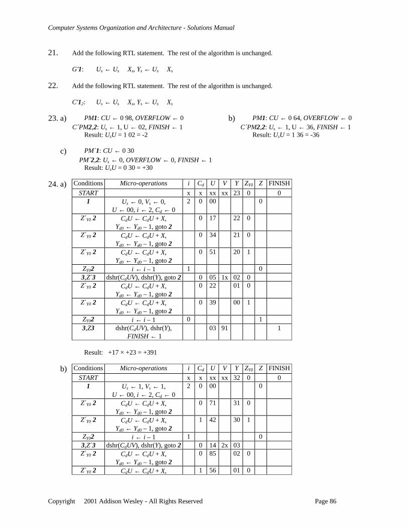
Computer Systems Organization and Architecture - Solutions Manual
Copyright 2001 Addison Wesley - All Rights Reserved Page 86
21. Add the following RTL statement. The rest of the algorithm is unchanged.
G'1: Us ← Us ⊕ Xs, Ys ← Us ⊕ Xs
22. Add the following RTL statement. The rest of the algorithm is unchanged.
C'12: Us ← Us ⊕ Xs, Ys ← Us ⊕ Xs
23. a) PM1: CU ← 0 98, OVERFLOW ← 0 b) PM1: CU ← 0 64, OVERFLOW ← 0C´PM2,2: Us ← 1, U ← 02, FINISH ← 1 C´PM2,2: Us ← 1, U ← 36, FINISH ← 1
Result: UsU = 1 02 = -2 Result: UsU = 1 36 = -36
c) PM´1: CU ← 0 30 PM´2,2: Us ← 0, OVERFLOW ← 0, FINISH ← 1
Result: UsU = 0 30 = +30
24. a) Conditions Micro-operations i Cd U V Y ZY0 Z FINISH
START x x xx xx 23 0 01 Us ← 0, Vs ← 0,
U ← 00, i ← 2, Cd ← 02 0 00 0
Z´Y0 2 CdU ← CdU + X,Yd0 ← Yd0 – 1, goto 2
0 17 22 0
Z´Y0 2 CdU ← CdU + X,Yd0 ← Yd0 – 1, goto 2
0 34 21 0
Z´Y0 2 CdU ← CdU + X,Yd0 ← Yd0 – 1, goto 2
0 51 20 1
ZY02 i ← i – 1 1 03,Z´3 dshr(CdUV), dshr(Y), goto 2 0 05 1x 02 0Z´Y0 2 CdU ← CdU + X,
Yd0 ← Yd0 – 1, goto 20 22 01 0
Z´Y0 2 CdU ← CdU + X,Yd0 ← Yd0 – 1, goto 2
0 39 00 1
ZY02 i ← i – 1 0 13,Z3 dshr(CdUV), dshr(Y),
FINISH ← 103 91 1
Result: +17 × +23 = +391
b) Conditions Micro-operations i Cd U V Y ZY0 Z FINISH
START x x xx xx 32 0 01 Us ← 1, Vs ← 1,
U ← 00, i ← 2, Cd ← 02 0 00 0
Z´Y0 2 CdU ← CdU + X,Yd0 ← Yd0 – 1, goto 2
0 71 31 0
Z´Y0 2 CdU ← CdU + X,Yd0 ← Yd0 – 1, goto 2
1 42 30 1
ZY02 i ← i – 1 1 03,Z´3 dshr(CdUV), dshr(Y), goto 2 0 14 2x 03Z´Y0 2 CdU ← CdU + X,
Yd0 ← Yd0 – 1, goto 20 85 02 0
Z´Y0 2 CdU ← CdU + X, 1 56 01 0
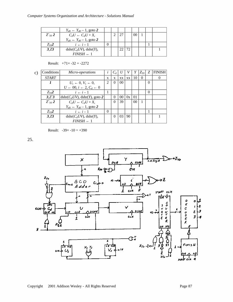
Computer Systems Organization and Architecture - Solutions Manual
Copyright 2001 Addison Wesley - All Rights Reserved Page 87
Yd0 ← Yd0 – 1, goto 2Z´Y0 2 CdU ← CdU + X,
Yd0 ← Yd0 – 1, goto 22 27 00 1
ZY02 i ← i – 1 0 13,Z3 dshr(CdUV), dshr(Y),
FINISH ← 122 72 1
Result: +71× -32 = -2272
c) Conditions Micro-operations i Cd U V Y ZY0 Z FINISH
START x x xx xx 10 0 01 Us ← 0, Vs ← 0,
U ← 00, i ← 2, Cd ← 02 0 00 0
ZY02 i ← i – 1 1 03,Z´3 dshr(CdUV), dshr(Y), goto 2 0 00 0x 01Z´Y0 2 CdU ← CdU + X,
Yd0 ← Yd0 – 1, goto 20 39 00 1
ZY02 i ← i – 1 0 13,Z3 dshr(CdUV), dshr(Y),
FINISH ← 10 03 90 1
Result: -39× -10 = +390
25.
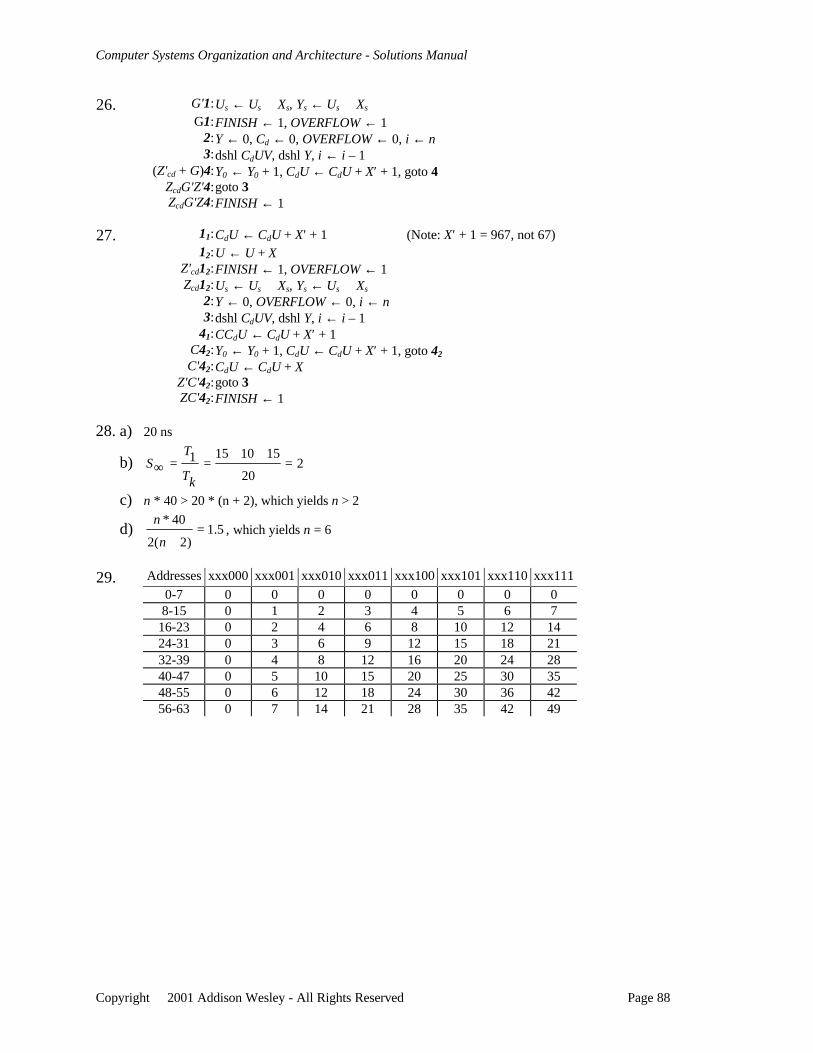
Computer Systems Organization and Architecture - Solutions Manual
Copyright 2001 Addison Wesley - All Rights Reserved Page 88
26. G'1:Us ← Us ⊕ Xs, Ys ← Us ⊕ Xs
G1:FINISH ← 1, OVERFLOW ← 12:Y ← 0, Cd ← 0, OVERFLOW ← 0, i ← n3:dshl CdUV, dshl Y, i ← i – 1
(Z'cd + G)4:Y0 ← Y0 + 1, CdU ← CdU + X′ + 1, goto 4ZcdG'Z'4:goto 3ZcdG'Z4:FINISH ← 1
27. 11:CdU ← CdU + X′ + 1 (Note: X′ + 1 = 967, not 67)12:U ← U + X
Z'cd12:FINISH ← 1, OVERFLOW ← 1Zcd12:Us ← Us ⊕ Xs, Ys ← Us ⊕ Xs
2:Y ← 0, OVERFLOW ← 0, i ← n3:dshl CdUV, dshl Y, i ← i – 1
41:CCdU ← CdU + X′ + 1C42:Y0 ← Y0 + 1, CdU ← CdU + X′ + 1, goto 42
C'42:CdU ← CdU + XZ'C'42:goto 3ZC'42:FINISH ← 1
28. a) 20 ns
b) 220
1510151 =++
==∞kT
TS
c) n * 40 > 20 * (n + 2), which yields n > 2
d) 5.1)2(2
40*=
+n
n, which yields n = 6
29. Addresses xxx000 xxx001 xxx010 xxx011 xxx100 xxx101 xxx110 xxx111
0-7 0 0 0 0 0 0 0 08-15 0 1 2 3 4 5 6 7
16-23 0 2 4 6 8 10 12 1424-31 0 3 6 9 12 15 18 2132-39 0 4 8 12 16 20 24 2840-47 0 5 10 15 20 25 30 3548-55 0 6 12 18 24 30 36 4256-63 0 7 14 21 28 35 42 49
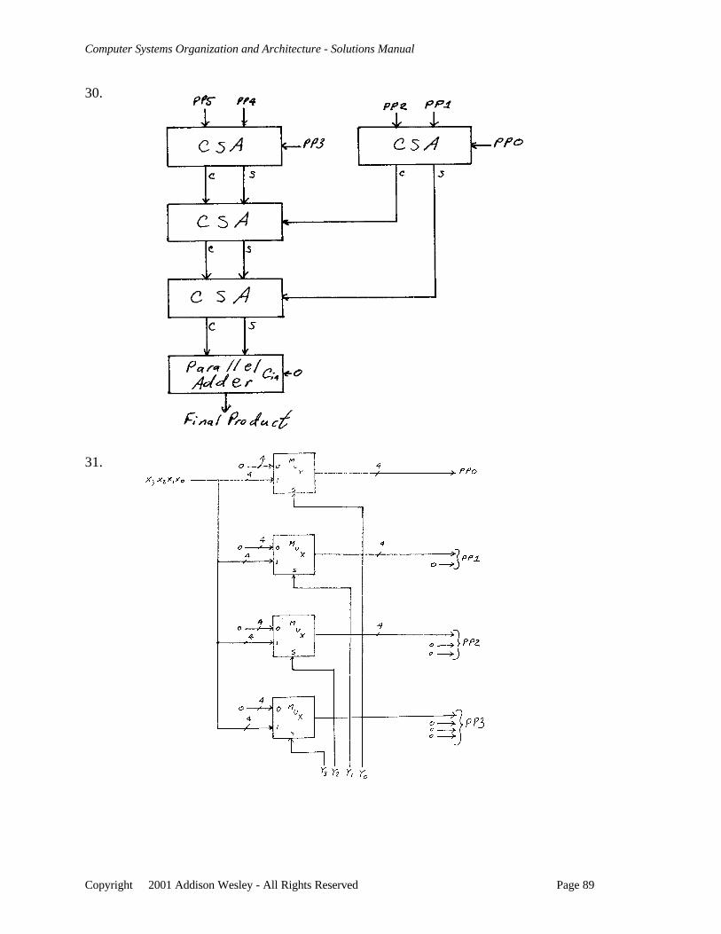
Computer Systems Organization and Architecture - Solutions Manual
Copyright 2001 Addison Wesley - All Rights Reserved Page 89
30.
31.
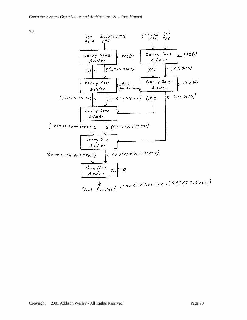
Computer Systems Organization and Architecture - Solutions Manual
Copyright 2001 Addison Wesley - All Rights Reserved Page 90
32.
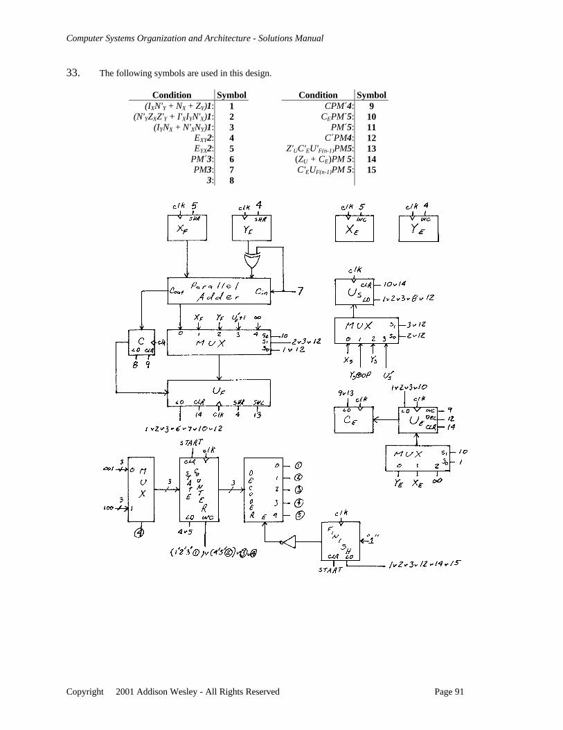
Computer Systems Organization and Architecture - Solutions Manual
Copyright 2001 Addison Wesley - All Rights Reserved Page 91
33. The following symbols are used in this design.
Condition Symbol Condition Symbol(IXN'Y + NX + ZY)1: 1 CPM´4: 9
(N'YZXZ'Y + I'XIYN'X)1: 2 CEPM´5: 10(IYNX + N'XNY)1: 3 PM´5: 11
EXY2: 4 C´PM4: 12EYX2: 5 Z'UC'EU'F(n-1)PM5: 13
PM´3: 6 (ZU + CE)PM 5: 14PM3: 7 C'EUF(n-1)PM 5: 15
3: 8
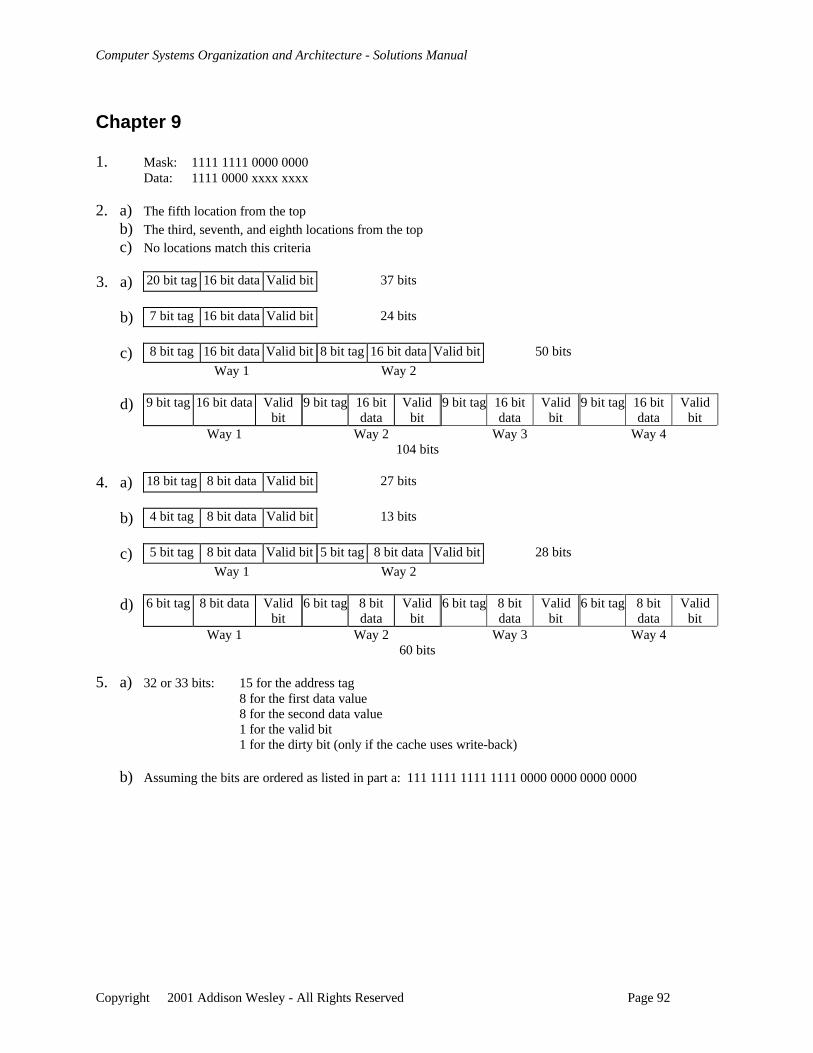
Computer Systems Organization and Architecture - Solutions Manual
Copyright 2001 Addison Wesley - All Rights Reserved Page 92
Chapter 9
1. Mask: 1111 1111 0000 0000Data: 1111 0000 xxxx xxxx
2. a) The fifth location from the topb) The third, seventh, and eighth locations from the topc) No locations match this criteria
3. a) 20 bit tag 16 bit data Valid bit 37 bits
b) 7 bit tag 16 bit data Valid bit 24 bits
c) 8 bit tag 16 bit data Valid bit 8 bit tag 16 bit data Valid bit 50 bits
Way 1 Way 2
d) 9 bit tag 16 bit data Validbit
9 bit tag 16 bitdata
Validbit
9 bit tag 16 bitdata
Validbit
9 bit tag 16 bitdata
Validbit
Way 1 Way 2 Way 3 Way 4104 bits
4. a) 18 bit tag 8 bit data Valid bit 27 bits
b) 4 bit tag 8 bit data Valid bit 13 bits
c) 5 bit tag 8 bit data Valid bit 5 bit tag 8 bit data Valid bit 28 bits
Way 1 Way 2
d) 6 bit tag 8 bit data Validbit
6 bit tag 8 bitdata
Validbit
6 bit tag 8 bitdata
Validbit
6 bit tag 8 bitdata
Validbit
Way 1 Way 2 Way 3 Way 460 bits
5. a) 32 or 33 bits: 15 for the address tag8 for the first data value8 for the second data value1 for the valid bit1 for the dirty bit (only if the cache uses write-back)
b) Assuming the bits are ordered as listed in part a: 111 1111 1111 1111 0000 0000 0000 0000
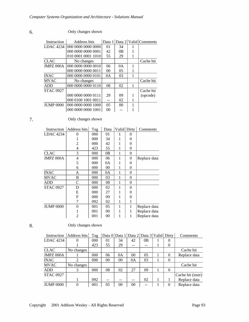
Computer Systems Organization and Architecture - Solutions Manual
Copyright 2001 Addison Wesley - All Rights Reserved Page 93
6. Only changes shown
Instruction Address bits Data 1 Data 2 Valid CommentsLDAC 4234 000 0000 0000 0000
000 0000 0000 0001010 0001 0001 1010
014255
340B29
111
CLAC No changes Cache hitJMPZ 000A 000 0000 0000 0010
000 0000 0000 00110600
0A05
11
INAC 000 0000 0000 0101 0A 03 1MVAC No changes Cache hitADD 000 0000 0000 0110 08 02 1STAC 0927
000 0000 0000 0111000 0100 1001 0011
29--
0902
11
Cache hit(opcode)
JUMP 0000 000 0000 0000 1000000 0000 0000 1001
0500
00--
11
7. Only changes shown
Instruction Address bits Tag Data Valid Dirty CommentsLDAC 4234 0
124
000000000423
01344255
1111
0000
CLAC 3 000 0B 1 0JMPZ 000A 4
56
000000000
060A00
111
000
Replace data
INAC A 000 0A 1 0MVAC B 000 03 1 0ADD C 000 08 1 0STAC 0927 D
EF7
000000000092
02270902
1111
0001
JUMP 0000 012
001001001
050000
111
111
Replace dataReplace dataReplace data
8. Only changes shown
Instruction Address bits Tag Data 0 Data 1 Data 2 Data 3 Valid Dirty CommentsLDAC 4234 0
1000423
0155
3429
42--
0B--
11
00
CLAC No changes Cache hitJMPZ 000A 1 000 06 0A 00 05 1 0 Replace dataINAC 2 000 00 00 0A 03 1 0MVAC No changes Cache hitADD 3 000 08 02 27 09 1 0STAC 0927
1 092 -- -- -- 02 1 1Cache hit (instr)
Replace dataJUMP 0000 0 001 05 00 00 -- 1 0 Replace data
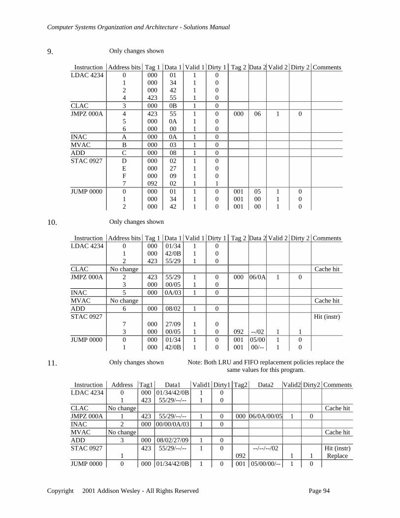
Computer Systems Organization and Architecture - Solutions Manual
Copyright 2001 Addison Wesley - All Rights Reserved Page 94
9. Only changes shown
Instruction Address bits Tag 1 Data 1 Valid 1 Dirty 1 Tag 2 Data 2 Valid 2 Dirty 2 CommentsLDAC 4234 0
124
000000000423
01344255
1111
0000
CLAC 3 000 0B 1 0JMPZ 000A 4
56
423000000
550A00
111
000
000 06 1 0
INAC A 000 0A 1 0MVAC B 000 03 1 0ADD C 000 08 1 0STAC 0927 D
EF7
000000000092
02270902
1111
0001
JUMP 0000 012
000000000
013442
111
000
001001001
050000
111
000
10. Only changes shown
Instruction Address bits Tag 1 Data 1 Valid 1 Dirty 1 Tag 2 Data 2 Valid 2 Dirty 2 CommentsLDAC 4234 0
12
000000423
01/3442/0B55/29
111
000
CLAC No change Cache hitJMPZ 000A 2
3423000
55/2900/05
11
00
000 06/0A 1 0
INAC 5 000 0A/03 1 0MVAC No change Cache hitADD 6 000 08/02 1 0STAC 0927
73
000000
27/0900/05
11
00 092 --/02 1 1
Hit (instr)
JUMP 0000 01
000000
01/3442/0B
11
00
001001
05/0000/--
11
00
11. Only changes shown Note: Both LRU and FIFO replacement policies replace thesame values for this program.
Instruction Address Tag1 Data1 Valid1 Dirty1 Tag2 Data2 Valid2 Dirty2 CommentsLDAC 4234 0
1000423
01/34/42/0B55/29/--/--
11
00
CLAC No change Cache hitJMPZ 000A 1 423 55/29/--/-- 1 0 000 06/0A/00/05 1 0INAC 2 000 00/00/0A/03 1 0MVAC No change Cache hitADD 3 000 08/02/27/09 1 0STAC 0927
1423 55/29/--/-- 1 0
092--/--/--/02
1 1Hit (instr)Replace
JUMP 0000 0 000 01/34/42/0B 1 0 001 05/00/00/-- 1 0
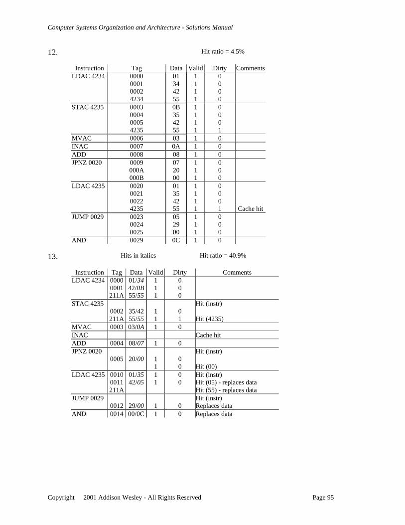
Computer Systems Organization and Architecture - Solutions Manual
Copyright 2001 Addison Wesley - All Rights Reserved Page 95
12. Hit ratio = 4.5%
Instruction Tag Data Valid Dirty CommentsLDAC 4234 0000
000100024234
01344255
1111
0000
STAC 4235 0003000400054235
0B354255
1111
0001
MVAC 0006 03 1 0INAC 0007 0A 1 0ADD 0008 08 1 0JPNZ 0020 0009
000A000B
072000
111
000
LDAC 4235 0020002100224235
01354255
1111
0001 Cache hit
JUMP 0029 002300240025
052900
111
000
AND 0029 0C 1 0
13. Hits in italics Hit ratio = 40.9%
Instruction Tag Data Valid Dirty CommentsLDAC 4234 0000
0001211A
01/3442/0B55/55
111
000
STAC 42350002211A
35/4255/55
11
01
Hit (instr)
Hit (4235)MVAC 0003 03/0A 1 0INAC Cache hitADD 0004 08/07 1 0JPNZ 0020
0005 20/00 11
00
Hit (instr)
Hit (00)LDAC 4235 0010
0011211A
01/3542/05
11
00
Hit (instr)Hit (05) - replaces dataHit (55) - replaces data
JUMP 00290012 29/00 1 0
Hit (instr)Replaces data
AND 0014 00/0C 1 0 Replaces data
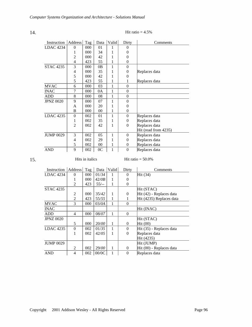
Computer Systems Organization and Architecture - Solutions Manual
Copyright 2001 Addison Wesley - All Rights Reserved Page 96
14. Hit ratio = 4.5%
Instruction Address Tag Data Valid Dirty CommentsLDAC 4234 0
124
000000000423
01344255
1111
0000
STAC 4235 3455
000000000423
0B354255
1111
0001
Replaces data
Replaces dataMVAC 6 000 03 1 0INAC 7 000 0A 1 0ADD 8 000 08 1 0JPNZ 0020 9
AB
000000000
072000
111
000
LDAC 4235 012
002002002
013542
111
000
Replaces dataReplaces dataReplaces dataHit (read from 4235)
JUMP 0029 345
002002002
052900
111
000
Replaces dataReplaces dataReplaces data
AND 9 002 0C 1 0 Replaces data
15. Hits in italics Hit ratio = 50.0%
Instruction Address Tag Data Valid Dirty CommentsLDAC 4234 0
12
000000423
01/3442/0B55/--
111
000
Hit (34)
STAC 423522
000423
35/4255/55
11
01
Hit (STAC)Hit (42) - Replaces dataHit (4235) Replaces data
MVAC 3 000 03/0A 1 0INAC Hit (INAC)ADD 4 000 08/07 1 0JPNZ 0020
5 000 20/00 1 0Hit (STAC)Hit (00)
LDAC 4235 01
002002
01/3542/05
11
00
Hit (35) - Replaces dataReplaces dataHit (4235)
JUMP 00292 002 29/00 1 0
Hit (JUMP)Hit (00) - Replaces data
AND 4 002 00/0C 1 0 Replaces data
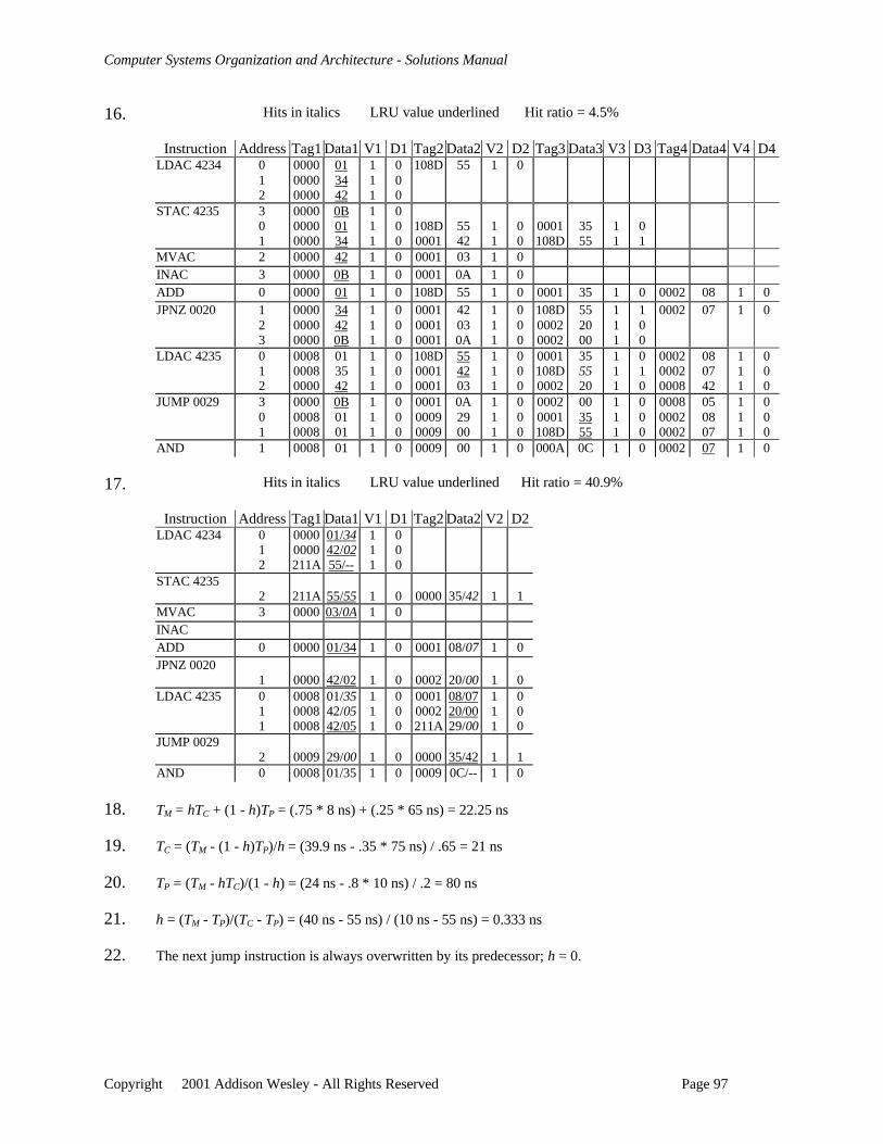
Computer Systems Organization and Architecture - Solutions Manual
Copyright 2001 Addison Wesley - All Rights Reserved Page 97
16. Hits in italics LRU value underlined Hit ratio = 4.5%
Instruction Address Tag1 Data1 V1 D1 Tag2 Data2 V2 D2 Tag3 Data3 V3 D3 Tag4 Data4 V4 D4LDAC 4234 0
12
000000000000
013442
111
000
108D 55 1 0
STAC 4235 301
000000000000
0B0134
111
000
108D0001
5542
11
00
0001108D
3555
11
01
MVAC 2 0000 42 1 0 0001 03 1 0INAC 3 0000 0B 1 0 0001 0A 1 0ADD 0 0000 01 1 0 108D 55 1 0 0001 35 1 0 0002 08 1 0JPNZ 0020 1
23
000000000000
34420B
111
000
000100010001
42030A
111
000
108D00020002
552000
111
100
0002 07 1 0
LDAC 4235 012
000800080000
013542
111
000
108D00010001
554203
111
000
0001108D0002
355520
111
010
000200020008
080742
111
000
JUMP 0029 301
000000080008
0B0101
111
000
000100090009
0A2900
111
000
00020001108D
003555
111
000
000800020002
050807
111
000
AND 1 0008 01 1 0 0009 00 1 0 000A 0C 1 0 0002 07 1 0
17. Hits in italics LRU value underlined Hit ratio = 40.9%
Instruction Address Tag1 Data1 V1 D1 Tag2 Data2 V2 D2LDAC 4234 0
12
00000000211A
01/3442/0255/--
111
000
STAC 42352 211A 55/55 1 0 0000 35/42 1 1
MVAC 3 0000 03/0A 1 0INACADD 0 0000 01/34 1 0 0001 08/07 1 0JPNZ 0020
1 0000 42/02 1 0 0002 20/00 1 0LDAC 4235 0
11
000800080008
01/3542/0542/05
111
000
00010002211A
08/0720/0029/00
111
000
JUMP 00292 0009 29/00 1 0 0000 35/42 1 1
AND 0 0008 01/35 1 0 0009 0C/-- 1 0
18. TM = hTC + (1 - h)TP = (.75 * 8 ns) + (.25 * 65 ns) = 22.25 ns
19. TC = (TM - (1 - h)TP)/h = (39.9 ns - .35 * 75 ns) / .65 = 21 ns
20. TP = (TM - hTC)/(1 - h) = (24 ns - .8 * 10 ns) / .2 = 80 ns
21. h = (TM - TP)/(TC - TP) = (40 ns - 55 ns) / (10 ns - 55 ns) = 0.333 ns
22. The next jump instruction is always overwritten by its predecessor; h = 0.
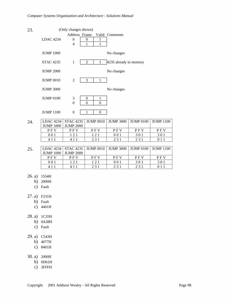
Computer Systems Organization and Architecture - Solutions Manual
Copyright 2001 Addison Wesley - All Rights Reserved Page 98
23. (Only changes shown)Address Frame Valid Comments
LDAC 4234 0 0 14 1 1
JUMP 1000 No changes
STAC 4235 1 2 1 4235 already in memory
JUMP 2000 No changes
JUMP 0010 2 3 1
JUMP 3000 No changes
JUMP 0100 3 0 10 0 0
JUMP 1100 0 1 0
24. LDAC 4234JUMP 1000
STAC 4235JUMP 2000
JUMP 0010 JUMP 3000 JUMP 0100 JUMP 1100
P F V P F V P F V P F V P F V P F V0 0 1 1 2 1 1 2 1 0 0 1 3 0 1 3 0 14 1 1 4 1 1 2 3 1 2 3 1 2 3 1 0 1 1
25. LDAC 4234JUMP 1000
STAC 4235JUMP 2000
JUMP 0010 JUMP 3000 JUMP 0100 JUMP 1100
P F V P F V P F V P F V P F V P F V0 0 1 1 2 1 1 2 1 0 0 1 3 0 1 3 0 14 1 1 4 1 1 2 3 1 2 3 1 2 3 1 0 1 1
26. a) 1554Hb) 2000Hc) Fault
27. a) F231Hb) Faultc) 4401H
28. a) 1C35Hb) 0A38Hc) Fault
29. a) C543Hb) 4077Hc) 8401H
30. a) 2000Hb) 0D61Hc) 3FFFH
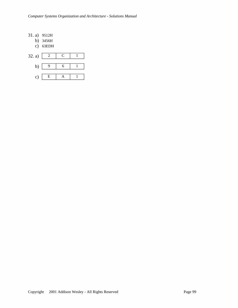
Computer Systems Organization and Architecture - Solutions Manual
Copyright 2001 Addison Wesley - All Rights Reserved Page 99
31. a) 9512Hb) 3456Hc) 63EDH
32. a) 2 C 1
b) 9 6 1
c) E A 1
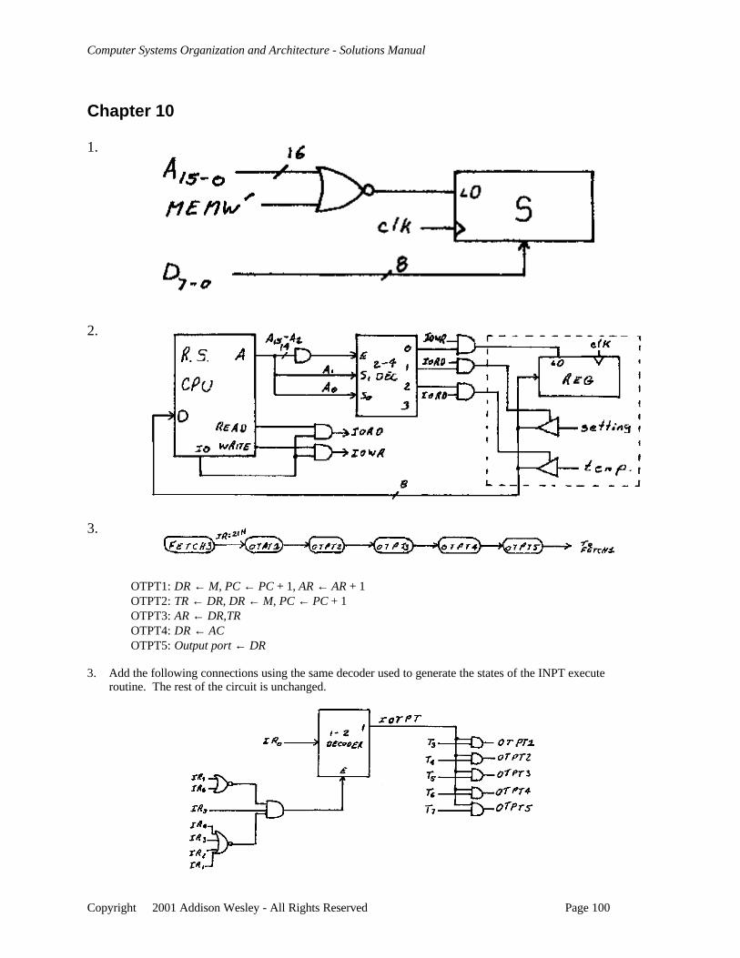
Computer Systems Organization and Architecture - Solutions Manual
Copyright 2001 Addison Wesley - All Rights Reserved Page 100
Chapter 10
1.
2.
3.
OTPT1: DR ← M, PC ← PC + 1, AR ← AR + 1OTPT2: TR ← DR, DR ← M, PC ← PC + 1OTPT3: AR ← DR,TROTPT4: DR ← ACOTPT5: Output port ← DR
3. Add the following connections using the same decoder used to generate the states of the INPT executeroutine. The rest of the circuit is unchanged.
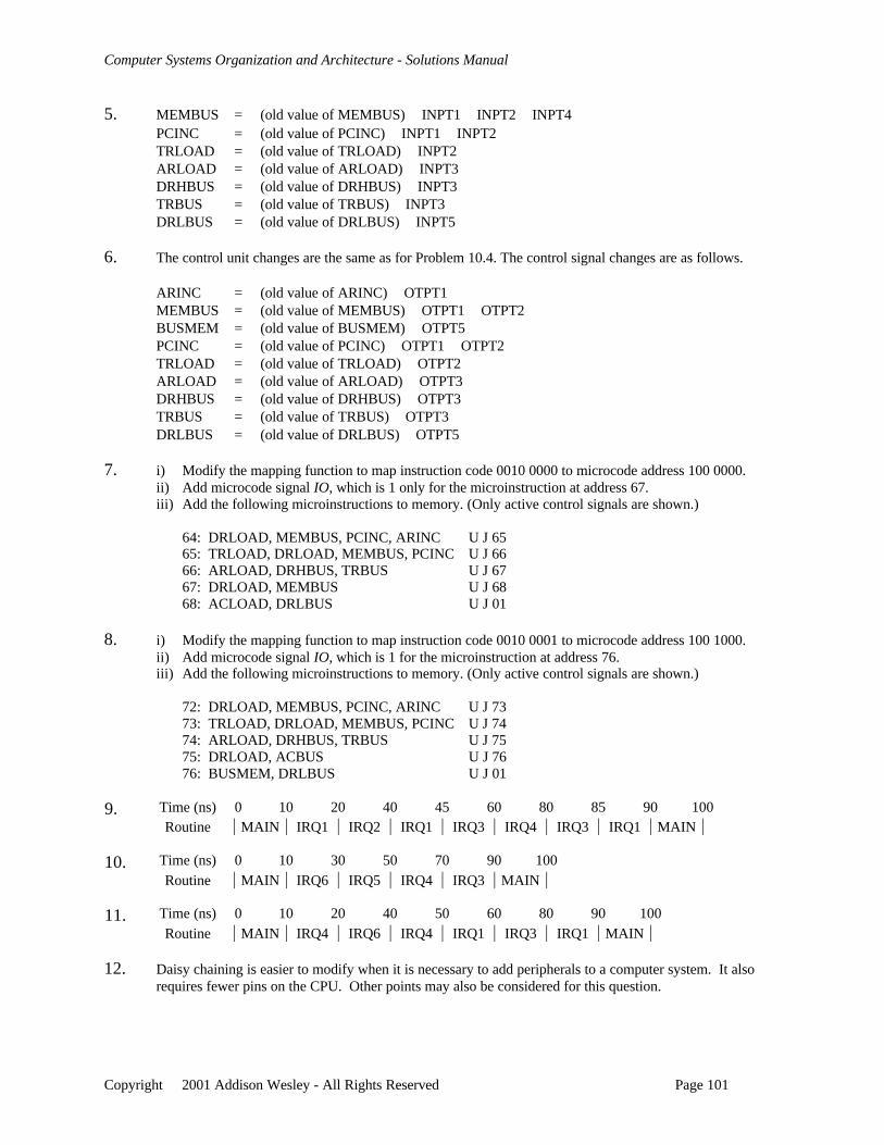
Computer Systems Organization and Architecture - Solutions Manual
Copyright 2001 Addison Wesley - All Rights Reserved Page 101
5. MEMBUS = (old value of MEMBUS) ∨ INPT1 ∨ INPT2 ∨ INPT4PCINC = (old value of PCINC) ∨ INPT1 ∨ INPT2TRLOAD = (old value of TRLOAD) ∨ INPT2ARLOAD = (old value of ARLOAD) ∨ INPT3DRHBUS = (old value of DRHBUS) ∨ INPT3TRBUS = (old value of TRBUS) ∨ INPT3DRLBUS = (old value of DRLBUS) ∨ INPT5
6. The control unit changes are the same as for Problem 10.4. The control signal changes are as follows.
ARINC = (old value of ARINC) ∨ OTPT1MEMBUS = (old value of MEMBUS) ∨ OTPT1 ∨ OTPT2BUSMEM = (old value of BUSMEM) ∨ OTPT5PCINC = (old value of PCINC) ∨ OTPT1 ∨ OTPT2TRLOAD = (old value of TRLOAD) ∨ OTPT2ARLOAD = (old value of ARLOAD) ∨ OTPT3DRHBUS = (old value of DRHBUS) ∨ OTPT3TRBUS = (old value of TRBUS) ∨ OTPT3DRLBUS = (old value of DRLBUS) ∨ OTPT5
7. i) Modify the mapping function to map instruction code 0010 0000 to microcode address 100 0000.ii) Add microcode signal IO, which is 1 only for the microinstruction at address 67.iii) Add the following microinstructions to memory. (Only active control signals are shown.)
64: DRLOAD, MEMBUS, PCINC, ARINC U J 6565: TRLOAD, DRLOAD, MEMBUS, PCINC U J 6666: ARLOAD, DRHBUS, TRBUS U J 6767: DRLOAD, MEMBUS U J 6868: ACLOAD, DRLBUS U J 01
8. i) Modify the mapping function to map instruction code 0010 0001 to microcode address 100 1000.ii) Add microcode signal IO, which is 1 for the microinstruction at address 76.iii) Add the following microinstructions to memory. (Only active control signals are shown.)
72: DRLOAD, MEMBUS, PCINC, ARINC U J 7373: TRLOAD, DRLOAD, MEMBUS, PCINC U J 7474: ARLOAD, DRHBUS, TRBUS U J 7575: DRLOAD, ACBUS U J 7676: BUSMEM, DRLBUS U J 01
9. Time (ns) 0 10 20 40 45 60 80 85 90 100Routine MAIN IRQ1 IRQ2 IRQ1 IRQ3 IRQ4 IRQ3 IRQ1 MAIN
10. Time (ns) 0 10 30 50 70 90 100Routine MAIN IRQ6 IRQ5 IRQ4 IRQ3 MAIN
11. Time (ns) 0 10 20 40 50 60 80 90 100Routine MAIN IRQ4 IRQ6 IRQ4 IRQ1 IRQ3 IRQ1 MAIN
12. Daisy chaining is easier to modify when it is necessary to add peripherals to a computer system. It alsorequires fewer pins on the CPU. Other points may also be considered for this question.
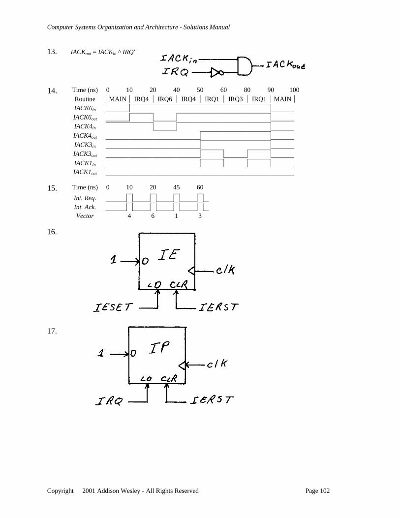
Computer Systems Organization and Architecture - Solutions Manual
Copyright 2001 Addison Wesley - All Rights Reserved Page 102
13. IACKout = IACKin ^ IRQ'
14. Time (ns) 0 10 20 40 50 60 80 90 100Routine MAIN IRQ4 IRQ6 IRQ4 IRQ1 IRQ3 IRQ1 MAINIACK6in
IACK6out
IACK4in
IACK4out
IACK3in
IACK3out
IACK1in
IACK1out
15. Time (ns) 0 10 20 45 60
Int. Req.
Int. Ack.Vector 4 6 1 3
16.
17.
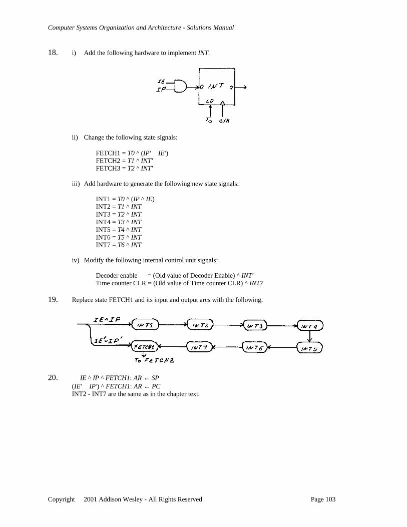
Computer Systems Organization and Architecture - Solutions Manual
Copyright 2001 Addison Wesley - All Rights Reserved Page 103
18. i) Add the following hardware to implement INT.
ii) Change the following state signals:
FETCH1 = T0 ^ (IP' ∨ IE')FETCH2 = T1 ^ INT'FETCH3 = T2 ^ INT'
iii) Add hardware to generate the following new state signals:
INT1 = T0 ^ (IP ^ IE)INT2 = T1 ^ INTINT3 = T2 ^ INTINT4 = T3 ^ INTINT5 = T4 ^ INTINT6 = T5 ^ INTINT7 = T6 ^ INT
iv) Modify the following internal control unit signals:
Decoder enable = (Old value of Decoder Enable) ^ INT'Time counter CLR = (Old value of Time counter CLR) ^ INT7
19. Replace state FETCH1 and its input and output arcs with the following.
20. IE ^ IP ^ FETCH1: AR ← SP(IE' ∨ IP') ^ FETCH1: AR ← PCINT2 - INT7 are the same as in the chapter text.
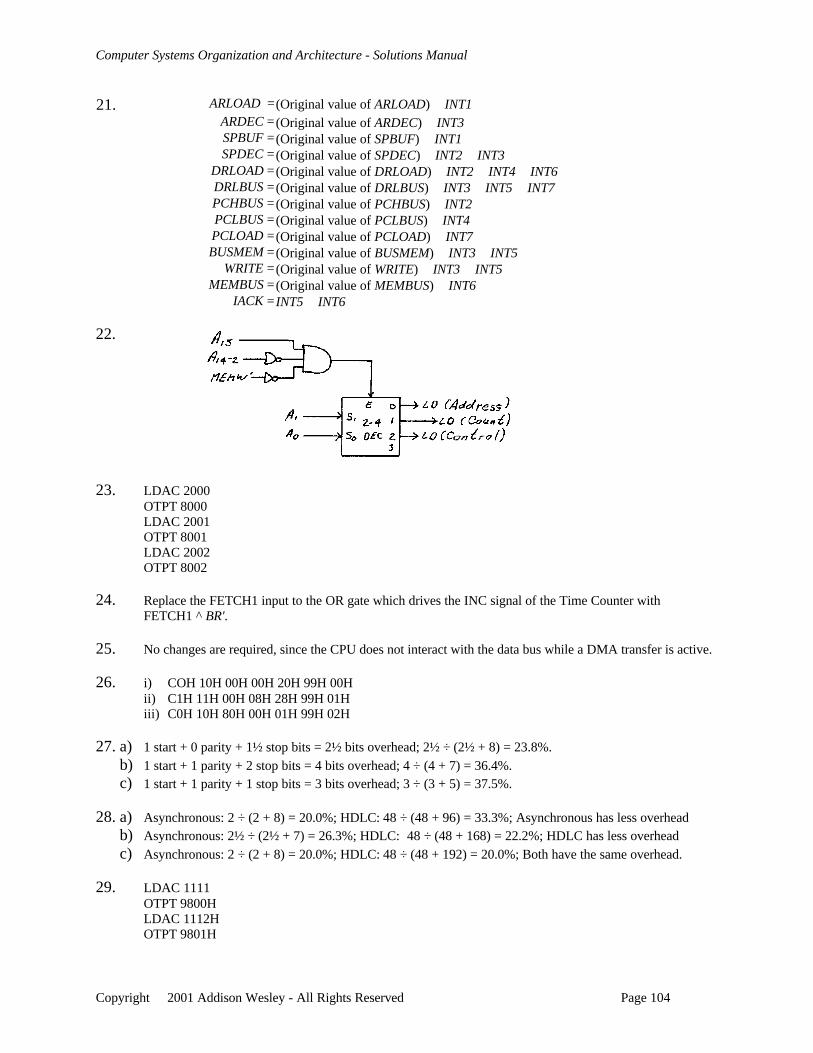
Computer Systems Organization and Architecture - Solutions Manual
Copyright 2001 Addison Wesley - All Rights Reserved Page 104
21. ARLOAD =(Original value of ARLOAD) ∨ INT1ARDEC =(Original value of ARDEC) ∨ INT3SPBUF =(Original value of SPBUF) ∨ INT1SPDEC =(Original value of SPDEC) ∨ INT2 ∨ INT3
DRLOAD =(Original value of DRLOAD) ∨ INT2 ∨ INT4 ∨ INT6DRLBUS =(Original value of DRLBUS) ∨ INT3 ∨ INT5 ∨ INT7PCHBUS =(Original value of PCHBUS) ∨ INT2PCLBUS =(Original value of PCLBUS) ∨ INT4PCLOAD =(Original value of PCLOAD) ∨ INT7BUSMEM =(Original value of BUSMEM) ∨ INT3 ∨ INT5
WRITE =(Original value of WRITE) ∨ INT3 ∨ INT5MEMBUS =(Original value of MEMBUS) ∨ INT6
IACK = INT5 ∨ INT6
22.
23. LDAC 2000OTPT 8000LDAC 2001OTPT 8001LDAC 2002OTPT 8002
24. Replace the FETCH1 input to the OR gate which drives the INC signal of the Time Counter withFETCH1 ^ BR'.
25. No changes are required, since the CPU does not interact with the data bus while a DMA transfer is active.
26. i) COH 10H 00H 00H 20H 99H 00Hii) C1H 11H 00H 08H 28H 99H 01Hiii) C0H 10H 80H 00H 01H 99H 02H
27. a) 1 start + 0 parity + 1½ stop bits = 2½ bits overhead; 2½ ÷ (2½ + 8) = 23.8%.b) 1 start + 1 parity + 2 stop bits = 4 bits overhead; 4 ÷ (4 + 7) = 36.4%.c) 1 start + 1 parity + 1 stop bits = 3 bits overhead; 3 ÷ (3 + 5) = 37.5%.
28. a) Asynchronous: 2 ÷ (2 + 8) = 20.0%; HDLC: 48 ÷ (48 + 96) = 33.3%; Asynchronous has less overheadb) Asynchronous: 2½ ÷ (2½ + 7) = 26.3%; HDLC: 48 ÷ (48 + 168) = 22.2%; HDLC has less overheadc) Asynchronous: 2 ÷ (2 + 8) = 20.0%; HDLC: 48 ÷ (48 + 192) = 20.0%; Both have the same overhead.
29. LDAC 1111OTPT 9800HLDAC 1112HOTPT 9801H
Computer Systems Organization and Architecture - Solutions Manual
Copyright 2001 Addison Wesley - All Rights Reserved Page 105
30. a) Token packet: 24 bitsData packet: 6168 bitsHandshaking packet: 8 bitsTOTAL: 6200 bits
b) 56 ÷ 6200 = 0.90%c) 1536 × (1 start bit + 8 data bits + 1 stop bit) = 15,360 bits
Computer Systems Organization and Architecture - Solutions Manual
Copyright 2001 Addison Wesley - All Rights Reserved Page 106
Chapter 11
1. a) 25 ns × 100% vs. (24 ns × 99%) + (24 ns × 4 instructions × 1%) average time25 ns vs. 23.76 ns + 0.96 ns25 ns > 24.72 ns, therefore the second CPU has better performance
b) 25 ns × 100% = (24 ns × (100 - x)%) + (96 ns × x%); x = 1.389%c) 25 ns × 100% = (24 ns × 99%) + (24 ns × x instructions × 1%); x = 5.167 instructionsd) x ns × 100% = (24 ns × 99%) + (96 ns × 1%); x = 24.72 nse) 25 ns × 100% = (x ns × 99%) + (4x ns × 1%); x = 24.272 ns
2. a) 15 ns × 100% vs. (12 ns × 98%) + (12 ns × 6 instructions × 2%) average time15 ns > 13.2 ns, therefore the second CPU has better performance
b) 15 ns × 100% = (12 ns × (100 - x)%) + (72 ns × x%); x = 5%c) 15 ns × 100% = (12 ns × 98%) + (12 ns × x instructions × 2%); x = 13.5 instructionsd) x ns × 100% = (12 ns × 98%) + (72 ns × 2%); x = 13.2 nse) 15 ns × 100% = (x ns × 98%) + (6x ns × 2%); x = 13.636 ns
3. a) 18 ns × 100% vs. (16 ns × 96%) + (16 ns × 5 instructions × 4%) average time18 ns > 18.56 ns, therefore the first CPU has better performance
b) 18 ns × 100% = (16 ns × (100 - x)%) + (80 ns × x%); x = 3.125%c) 18 ns × 100% = (16 ns × 96%) + (16 ns × x instructions × 4%); x = 4.125 instructionsd) x ns × 100% = (16 ns × 96%) + (80 ns × 4%); x = 18.56 nse) 18 ns × 100% = (x ns × 96%) + (5x ns × 4%); x = 15.517 ns
4. a) Clock period = 80 nsSteady state speedup = (40 + 80 + 50)/80 = 2.125
b) 160/80 = 2
5. a) Clock period = 60 nsSteady state speedup = (30 + 25 + 60 + 40)/60 = 2.583
b) 150/60 = 2.5
6. a) Clock period = 70 nsSteady state speedup = (20 + 25 + 20 + 70 + 40)/70 = 2.5
b) 160/70 = 2.286
7. a) Clock period = 50 nsSteady state speedup = (40 + 45 + 35 + 50)/50 = 3.4
b) 160/50 = 3.2
8. a) Clock period = 40 nsSteady state speedup = (30 + 25 + 20 + 40 + 40)/40 = 3.875
b) 150/40 = 3.75
9. a) Clock period = 45 nsSteady state speedup = (20 + 25 + 20 + 25 + 45 + 40)/45 = 3.889
b) 160/45 = 3.556c) Combine stages 1 and 2, and combine stages 3 and 4
Computer Systems Organization and Architecture - Solutions Manual
Copyright 2001 Addison Wesley - All Rights Reserved Page 107
10. 10 global registers + 8 windows × (4 input registers + 10 local registers) = 122 registersNote: Common output registers are not counted since they are already counted as common input
registers of the next window.
11. 160 registers = 16 global registers + W windows × (8 input registers + 16 local registers); W = 6 windows
12. 192 registers = 12 global registers + 10 windows × (6 input registers + L local registers);L = 12 local registers
13. 188 registers = 20 global registers + 12 windows × (C input registers + 10 local registers);C = 4 common input (and common output) registers
14. a) 2 no-opsb) 2 no-ops
15. a) 1:R1 ← R2 + R3 Stage\Cycle 1 2 3 4 5 6 7 8 9 10 11
N1:No-op 1 1 N1 2 N2 3 4 5 N3 62:R4 ← R1 + R2 2 - 1 N1 2 N2 3 4 5 N3 6
N2:No-op 3 - - 1 N1 2 N2 3 4 5 N3 63:R3 ← R1 + R44:R5 ← R2 + R65:R6 ← R1 + R2
N3:No-op6:R7 ← R5 + R6
b) 1:R1 ← R2 + R3 Stage\Cycle 1 2 3 4 5 6 7 8
4:R5 ← R2 + R6 1 1 4 2 5 3 62:R4 ← R1 + R2 2 - 1 4 2 5 3 65:R6 ← R1 + R2 3 - - 1 4 2 5 3 63:R3 ← R1 + R46:R7 ← R5 + R6
c) 1:R1 ← R2 + R3 Stage\Cycle 1 2 3 4 5 6 7 8 9 10 11
2:R4 ← R1 + R2 1 1 2 S 3 S 4 5 S 63:R3 ← R1 + R4 2 - 1 2 S 3 S 4 5 S 64:R5 ← R2 + R6 3 - - 1 2 S 3 S 4 5 S 65:R6 ← R1 + R26:R7 ← R5 + R6
d) 1:R1 ← R2 + R3 Stage\Cycle 1 2 3 4 5 6 7 8
2:R4 ← R1 + R2 1 1 2 3 4 5 63:R3 ← R1 + R4 2 - 1 2 3 4 5 64:R5 ← R2 + R6 3 - - 1 2 3 4 5 65:R6 ← R1 + R26:R7 ← R5 + R6
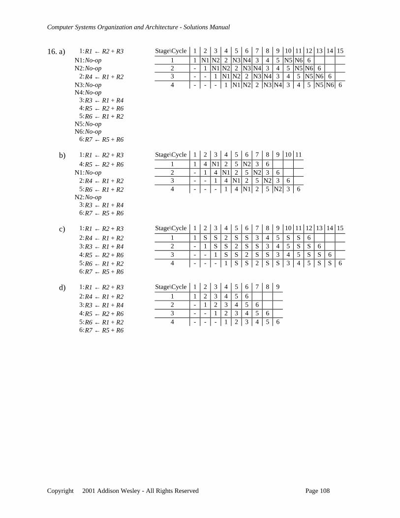
Computer Systems Organization and Architecture - Solutions Manual
Copyright 2001 Addison Wesley - All Rights Reserved Page 108
16. a) 1:R1 ← R2 + R3 Stage\Cycle 1 2 3 4 5 6 7 8 9 10 11 12 13 14 15
N1:No-op 1 1 N1 N2 2 N3 N4 3 4 5 N5 N6 6N2:No-op 2 - 1 N1 N2 2 N3 N4 3 4 5 N5 N6 6
2:R4 ← R1 + R2 3 - - 1 N1 N2 2 N3 N4 3 4 5 N5 N6 6N3:No-op 4 - - - 1 N1 N2 2 N3 N4 3 4 5 N5 N6 6N4:No-op
3:R3 ← R1 + R44:R5 ← R2 + R65:R6 ← R1 + R2
N5:No-opN6:No-op
6:R7 ← R5 + R6
b) 1:R1 ← R2 + R3 Stage\Cycle 1 2 3 4 5 6 7 8 9 10 11
4:R5 ← R2 + R6 1 1 4 N1 2 5 N2 3 6N1:No-op 2 - 1 4 N1 2 5 N2 3 6
2:R4 ← R1 + R2 3 - - 1 4 N1 2 5 N2 3 65:R6 ← R1 + R2 4 - - - 1 4 N1 2 5 N2 3 6
N2:No-op3:R3 ← R1 + R46:R7 ← R5 + R6
c) 1:R1 ← R2 + R3 Stage\Cycle 1 2 3 4 5 6 7 8 9 10 11 12 13 14 15
2:R4 ← R1 + R2 1 1 S S 2 S S 3 4 5 S S 63:R3 ← R1 + R4 2 - 1 S S 2 S S 3 4 5 S S 64:R5 ← R2 + R6 3 - - 1 S S 2 S S 3 4 5 S S 65:R6 ← R1 + R2 4 - - - 1 S S 2 S S 3 4 5 S S 66:R7 ← R5 + R6
d) 1:R1 ← R2 + R3 Stage\Cycle 1 2 3 4 5 6 7 8 9
2:R4 ← R1 + R2 1 1 2 3 4 5 63:R3 ← R1 + R4 2 - 1 2 3 4 5 64:R5 ← R2 + R6 3 - - 1 2 3 4 5 65:R6 ← R1 + R2 4 - - - 1 2 3 4 5 66:R7 ← R5 + R6
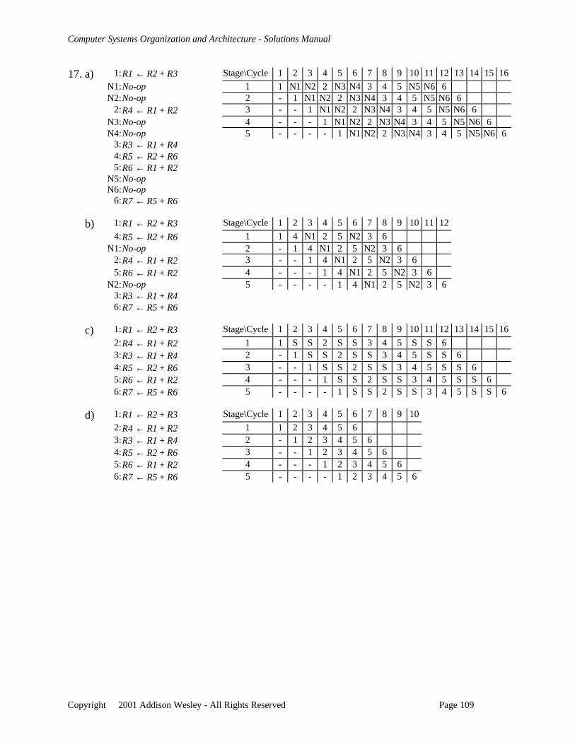
Computer Systems Organization and Architecture - Solutions Manual
Copyright 2001 Addison Wesley - All Rights Reserved Page 109
17. a) 1:R1 ← R2 + R3 Stage\Cycle 1 2 3 4 5 6 7 8 9 10 11 12 13 14 15 16
N1:No-op 1 1 N1 N2 2 N3 N4 3 4 5 N5 N6 6N2:No-op 2 - 1 N1 N2 2 N3 N4 3 4 5 N5 N6 6
2:R4 ← R1 + R2 3 - - 1 N1 N2 2 N3 N4 3 4 5 N5 N6 6N3:No-op 4 - - - 1 N1 N2 2 N3 N4 3 4 5 N5 N6 6N4:No-op 5 - - - - 1 N1 N2 2 N3 N4 3 4 5 N5 N6 6
3:R3 ← R1 + R44:R5 ← R2 + R65:R6 ← R1 + R2
N5:No-opN6:No-op
6:R7 ← R5 + R6
b) 1:R1 ← R2 + R3 Stage\Cycle 1 2 3 4 5 6 7 8 9 10 11 12
4:R5 ← R2 + R6 1 1 4 N1 2 5 N2 3 6N1:No-op 2 - 1 4 N1 2 5 N2 3 6
2:R4 ← R1 + R2 3 - - 1 4 N1 2 5 N2 3 65:R6 ← R1 + R2 4 - - - 1 4 N1 2 5 N2 3 6
N2:No-op 5 - - - - 1 4 N1 2 5 N2 3 63:R3 ← R1 + R46:R7 ← R5 + R6
c) 1:R1 ← R2 + R3 Stage\Cycle 1 2 3 4 5 6 7 8 9 10 11 12 13 14 15 16
2:R4 ← R1 + R2 1 1 S S 2 S S 3 4 5 S S 63:R3 ← R1 + R4 2 - 1 S S 2 S S 3 4 5 S S 64:R5 ← R2 + R6 3 - - 1 S S 2 S S 3 4 5 S S 65:R6 ← R1 + R2 4 - - - 1 S S 2 S S 3 4 5 S S 66:R7 ← R5 + R6 5 - - - - 1 S S 2 S S 3 4 5 S S 6
d) 1:R1 ← R2 + R3 Stage\Cycle 1 2 3 4 5 6 7 8 9 10
2:R4 ← R1 + R2 1 1 2 3 4 5 63:R3 ← R1 + R4 2 - 1 2 3 4 5 64:R5 ← R2 + R6 3 - - 1 2 3 4 5 65:R6 ← R1 + R2 4 - - - 1 2 3 4 5 66:R7 ← R5 + R6 5 - - - - 1 2 3 4 5 6
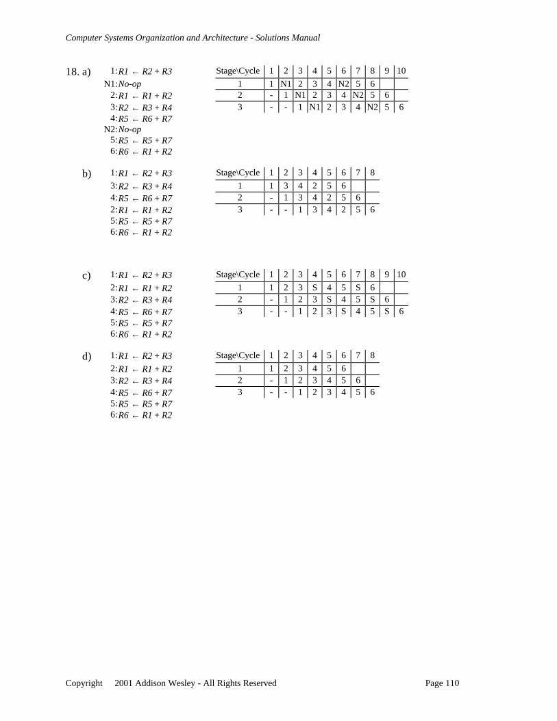
Computer Systems Organization and Architecture - Solutions Manual
Copyright 2001 Addison Wesley - All Rights Reserved Page 110
18. a) 1:R1 ← R2 + R3 Stage\Cycle 1 2 3 4 5 6 7 8 9 10
N1:No-op 1 1 N1 2 3 4 N2 5 62:R1 ← R1 + R2 2 - 1 N1 2 3 4 N2 5 63:R2 ← R3 + R4 3 - - 1 N1 2 3 4 N2 5 64:R5 ← R6 + R7
N2:No-op5:R5 ← R5 + R76:R6 ← R1 + R2
b) 1:R1 ← R2 + R3 Stage\Cycle 1 2 3 4 5 6 7 8
3:R2 ← R3 + R4 1 1 3 4 2 5 64:R5 ← R6 + R7 2 - 1 3 4 2 5 62:R1 ← R1 + R2 3 - - 1 3 4 2 5 65:R5 ← R5 + R76:R6 ← R1 + R2
c) 1:R1 ← R2 + R3 Stage\Cycle 1 2 3 4 5 6 7 8 9 10
2:R1 ← R1 + R2 1 1 2 3 S 4 5 S 63:R2 ← R3 + R4 2 - 1 2 3 S 4 5 S 64:R5 ← R6 + R7 3 - - 1 2 3 S 4 5 S 65:R5 ← R5 + R76:R6 ← R1 + R2
d) 1:R1 ← R2 + R3 Stage\Cycle 1 2 3 4 5 6 7 8
2:R1 ← R1 + R2 1 1 2 3 4 5 63:R2 ← R3 + R4 2 - 1 2 3 4 5 64:R5 ← R6 + R7 3 - - 1 2 3 4 5 65:R5 ← R5 + R76:R6 ← R1 + R2
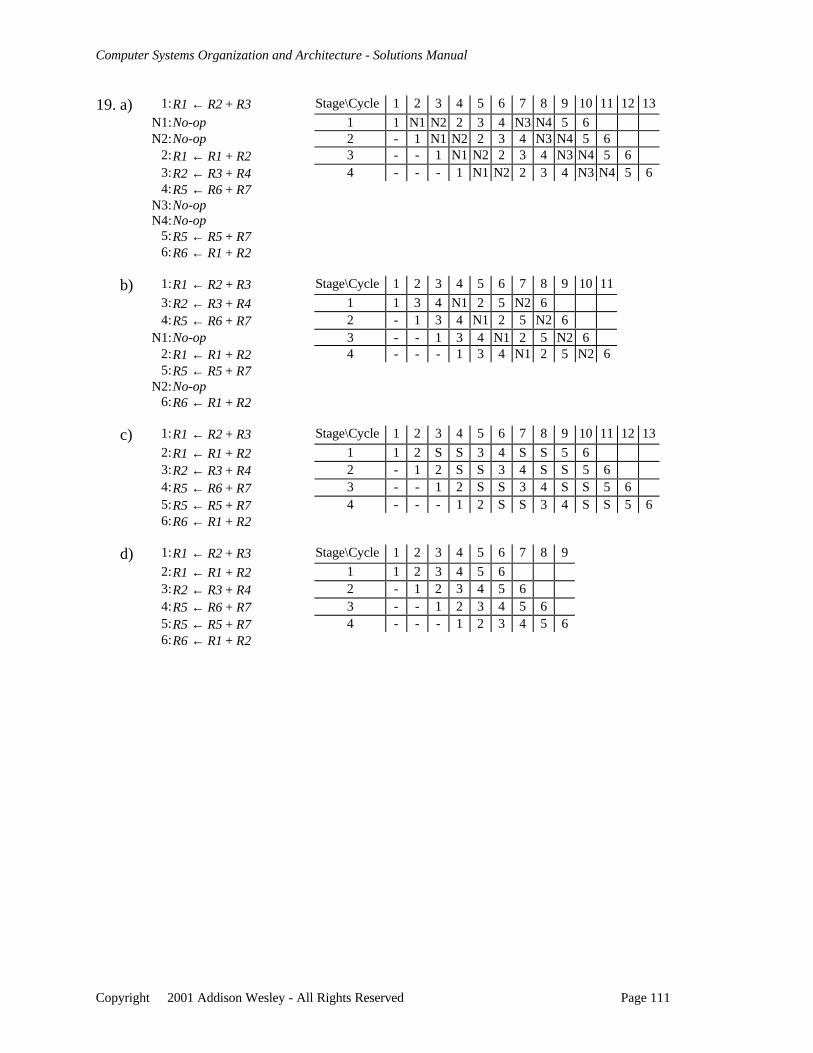
Computer Systems Organization and Architecture - Solutions Manual
Copyright 2001 Addison Wesley - All Rights Reserved Page 111
19. a) 1:R1 ← R2 + R3 Stage\Cycle 1 2 3 4 5 6 7 8 9 10 11 12 13
N1:No-op 1 1 N1 N2 2 3 4 N3 N4 5 6N2:No-op 2 - 1 N1 N2 2 3 4 N3 N4 5 6
2:R1 ← R1 + R2 3 - - 1 N1 N2 2 3 4 N3 N4 5 63:R2 ← R3 + R4 4 - - - 1 N1 N2 2 3 4 N3 N4 5 64:R5 ← R6 + R7
N3:No-opN4:No-op
5:R5 ← R5 + R76:R6 ← R1 + R2
b) 1:R1 ← R2 + R3 Stage\Cycle 1 2 3 4 5 6 7 8 9 10 11
3:R2 ← R3 + R4 1 1 3 4 N1 2 5 N2 64:R5 ← R6 + R7 2 - 1 3 4 N1 2 5 N2 6
N1:No-op 3 - - 1 3 4 N1 2 5 N2 62:R1 ← R1 + R2 4 - - - 1 3 4 N1 2 5 N2 65:R5 ← R5 + R7
N2:No-op6:R6 ← R1 + R2
c) 1:R1 ← R2 + R3 Stage\Cycle 1 2 3 4 5 6 7 8 9 10 11 12 13
2:R1 ← R1 + R2 1 1 2 S S 3 4 S S 5 63:R2 ← R3 + R4 2 - 1 2 S S 3 4 S S 5 64:R5 ← R6 + R7 3 - - 1 2 S S 3 4 S S 5 65:R5 ← R5 + R7 4 - - - 1 2 S S 3 4 S S 5 66:R6 ← R1 + R2
d) 1:R1 ← R2 + R3 Stage\Cycle 1 2 3 4 5 6 7 8 9
2:R1 ← R1 + R2 1 1 2 3 4 5 63:R2 ← R3 + R4 2 - 1 2 3 4 5 64:R5 ← R6 + R7 3 - - 1 2 3 4 5 65:R5 ← R5 + R7 4 - - - 1 2 3 4 5 66:R6 ← R1 + R2
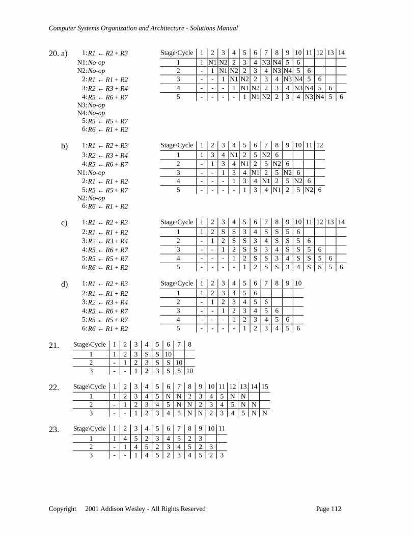
Computer Systems Organization and Architecture - Solutions Manual
Copyright 2001 Addison Wesley - All Rights Reserved Page 112
20. a) 1:R1 ← R2 + R3 Stage\Cycle 1 2 3 4 5 6 7 8 9 10 11 12 13 14
N1:No-op 1 1 N1 N2 2 3 4 N3 N4 5 6N2:No-op 2 - 1 N1 N2 2 3 4 N3 N4 5 6
2:R1 ← R1 + R2 3 - - 1 N1 N2 2 3 4 N3 N4 5 63:R2 ← R3 + R4 4 - - - 1 N1 N2 2 3 4 N3 N4 5 64:R5 ← R6 + R7 5 - - - - 1 N1 N2 2 3 4 N3 N4 5 6
N3:No-opN4:No-op
5:R5 ← R5 + R76:R6 ← R1 + R2
b) 1:R1 ← R2 + R3 Stage\Cycle 1 2 3 4 5 6 7 8 9 10 11 12
3:R2 ← R3 + R4 1 1 3 4 N1 2 5 N2 64:R5 ← R6 + R7 2 - 1 3 4 N1 2 5 N2 6
N1:No-op 3 - - 1 3 4 N1 2 5 N2 62:R1 ← R1 + R2 4 - - - 1 3 4 N1 2 5 N2 65:R5 ← R5 + R7 5 - - - - 1 3 4 N1 2 5 N2 6
N2:No-op6:R6 ← R1 + R2
c) 1:R1 ← R2 + R3 Stage\Cycle 1 2 3 4 5 6 7 8 9 10 11 12 13 14
2:R1 ← R1 + R2 1 1 2 S S 3 4 S S 5 63:R2 ← R3 + R4 2 - 1 2 S S 3 4 S S 5 64:R5 ← R6 + R7 3 - - 1 2 S S 3 4 S S 5 65:R5 ← R5 + R7 4 - - - 1 2 S S 3 4 S S 5 66:R6 ← R1 + R2 5 - - - - 1 2 S S 3 4 S S 5 6
d) 1:R1 ← R2 + R3 Stage\Cycle 1 2 3 4 5 6 7 8 9 10
2:R1 ← R1 + R2 1 1 2 3 4 5 63:R2 ← R3 + R4 2 - 1 2 3 4 5 64:R5 ← R6 + R7 3 - - 1 2 3 4 5 65:R5 ← R5 + R7 4 - - - 1 2 3 4 5 66:R6 ← R1 + R2 5 - - - - 1 2 3 4 5 6
21. Stage\Cycle 1 2 3 4 5 6 7 8
1 1 2 3 S S 102 - 1 2 3 S S 103 - - 1 2 3 S S 10
22. Stage\Cycle 1 2 3 4 5 6 7 8 9 10 11 12 13 14 15
1 1 2 3 4 5 N N 2 3 4 5 N N2 - 1 2 3 4 5 N N 2 3 4 5 N N3 - - 1 2 3 4 5 N N 2 3 4 5 N N
23. Stage\Cycle 1 2 3 4 5 6 7 8 9 10 11
1 1 4 5 2 3 4 5 2 32 - 1 4 5 2 3 4 5 2 33 - - 1 4 5 2 3 4 5 2 3
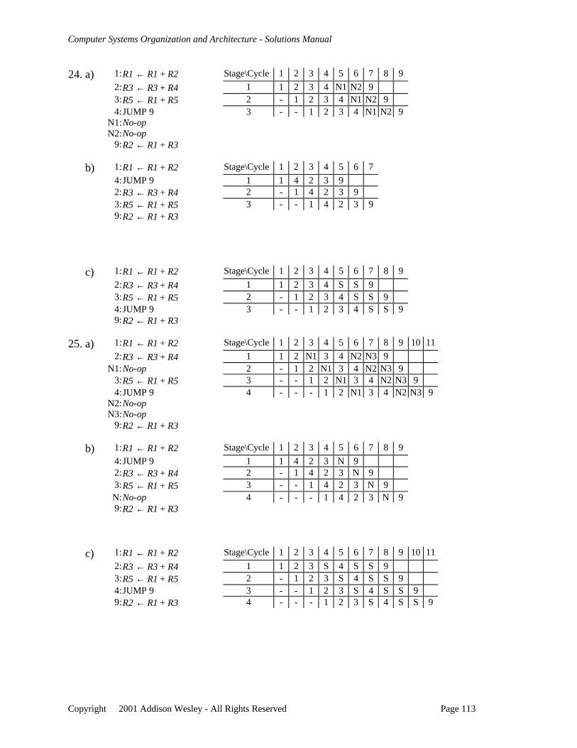
Computer Systems Organization and Architecture - Solutions Manual
Copyright 2001 Addison Wesley - All Rights Reserved Page 113
24. a) 1:R1 ← R1 + R2 Stage\Cycle 1 2 3 4 5 6 7 8 9
2:R3 ← R3 + R4 1 1 2 3 4 N1 N2 93:R5 ← R1 + R5 2 - 1 2 3 4 N1 N2 94:JUMP 9 3 - - 1 2 3 4 N1 N2 9
N1:No-opN2:No-op
9:R2 ← R1 + R3
b) 1:R1 ← R1 + R2 Stage\Cycle 1 2 3 4 5 6 7
4:JUMP 9 1 1 4 2 3 92:R3 ← R3 + R4 2 - 1 4 2 3 93:R5 ← R1 + R5 3 - - 1 4 2 3 99:R2 ← R1 + R3
c) 1:R1 ← R1 + R2 Stage\Cycle 1 2 3 4 5 6 7 8 9
2:R3 ← R3 + R4 1 1 2 3 4 S S 93:R5 ← R1 + R5 2 - 1 2 3 4 S S 94:JUMP 9 3 - - 1 2 3 4 S S 99:R2 ← R1 + R3
25. a) 1:R1 ← R1 + R2 Stage\Cycle 1 2 3 4 5 6 7 8 9 10 11
2:R3 ← R3 + R4 1 1 2 N1 3 4 N2 N3 9N1:No-op 2 - 1 2 N1 3 4 N2 N3 9
3:R5 ← R1 + R5 3 - - 1 2 N1 3 4 N2 N3 94:JUMP 9 4 - - - 1 2 N1 3 4 N2 N3 9
N2:No-opN3:No-op
9:R2 ← R1 + R3
b) 1:R1 ← R1 + R2 Stage\Cycle 1 2 3 4 5 6 7 8 9
4:JUMP 9 1 1 4 2 3 N 92:R3 ← R3 + R4 2 - 1 4 2 3 N 93:R5 ← R1 + R5 3 - - 1 4 2 3 N 9N:No-op 4 - - - 1 4 2 3 N 99:R2 ← R1 + R3
c) 1:R1 ← R1 + R2 Stage\Cycle 1 2 3 4 5 6 7 8 9 10 11
2:R3 ← R3 + R4 1 1 2 3 S 4 S S 93:R5 ← R1 + R5 2 - 1 2 3 S 4 S S 94:JUMP 9 3 - - 1 2 3 S 4 S S 99:R2 ← R1 + R3 4 - - - 1 2 3 S 4 S S 9
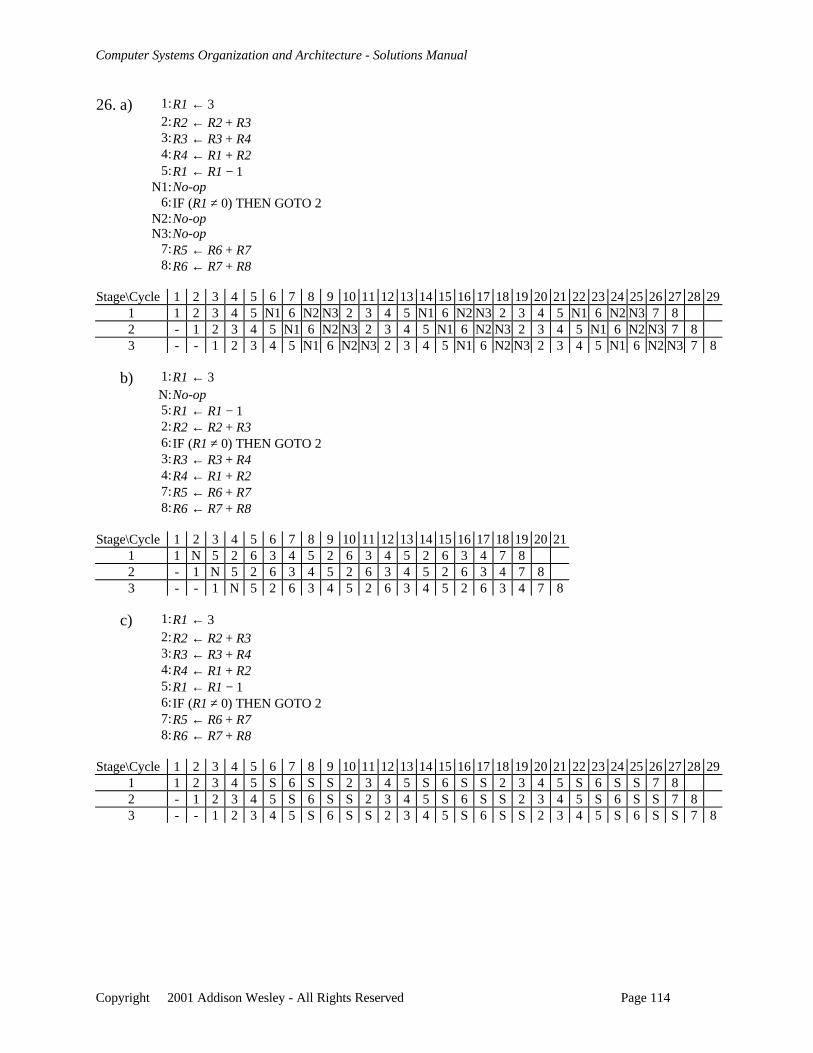
Computer Systems Organization and Architecture - Solutions Manual
Copyright 2001 Addison Wesley - All Rights Reserved Page 114
26. a) 1:R1 ← 32:R2 ← R2 + R33:R3 ← R3 + R44:R4 ← R1 + R25:R1 ← R1 − 1
N1:No-op6:IF (R1 ≠ 0) THEN GOTO 2
N2:No-opN3:No-op
7:R5 ← R6 + R78:R6 ← R7 + R8
Stage\Cycle 1 2 3 4 5 6 7 8 9 10 11 12 13 14 15 16 17 18 19 20 21 22 23 24 25 26 27 28 291 1 2 3 4 5 N1 6 N2 N3 2 3 4 5 N1 6 N2 N3 2 3 4 5 N1 6 N2 N3 7 82 - 1 2 3 4 5 N1 6 N2 N3 2 3 4 5 N1 6 N2 N3 2 3 4 5 N1 6 N2 N3 7 83 - - 1 2 3 4 5 N1 6 N2 N3 2 3 4 5 N1 6 N2 N3 2 3 4 5 N1 6 N2 N3 7 8
b) 1:R1 ← 3N:No-op5:R1 ← R1 − 12:R2 ← R2 + R36:IF (R1 ≠ 0) THEN GOTO 23:R3 ← R3 + R44:R4 ← R1 + R27:R5 ← R6 + R78:R6 ← R7 + R8
Stage\Cycle 1 2 3 4 5 6 7 8 9 10 11 12 13 14 15 16 17 18 19 20 211 1 N 5 2 6 3 4 5 2 6 3 4 5 2 6 3 4 7 82 - 1 N 5 2 6 3 4 5 2 6 3 4 5 2 6 3 4 7 83 - - 1 N 5 2 6 3 4 5 2 6 3 4 5 2 6 3 4 7 8
c) 1:R1 ← 32:R2 ← R2 + R33:R3 ← R3 + R44:R4 ← R1 + R25:R1 ← R1 − 16:IF (R1 ≠ 0) THEN GOTO 27:R5 ← R6 + R78:R6 ← R7 + R8
Stage\Cycle 1 2 3 4 5 6 7 8 9 10 11 12 13 14 15 16 17 18 19 20 21 22 23 24 25 26 27 28 291 1 2 3 4 5 S 6 S S 2 3 4 5 S 6 S S 2 3 4 5 S 6 S S 7 82 - 1 2 3 4 5 S 6 S S 2 3 4 5 S 6 S S 2 3 4 5 S 6 S S 7 83 - - 1 2 3 4 5 S 6 S S 2 3 4 5 S 6 S S 2 3 4 5 S 6 S S 7 8
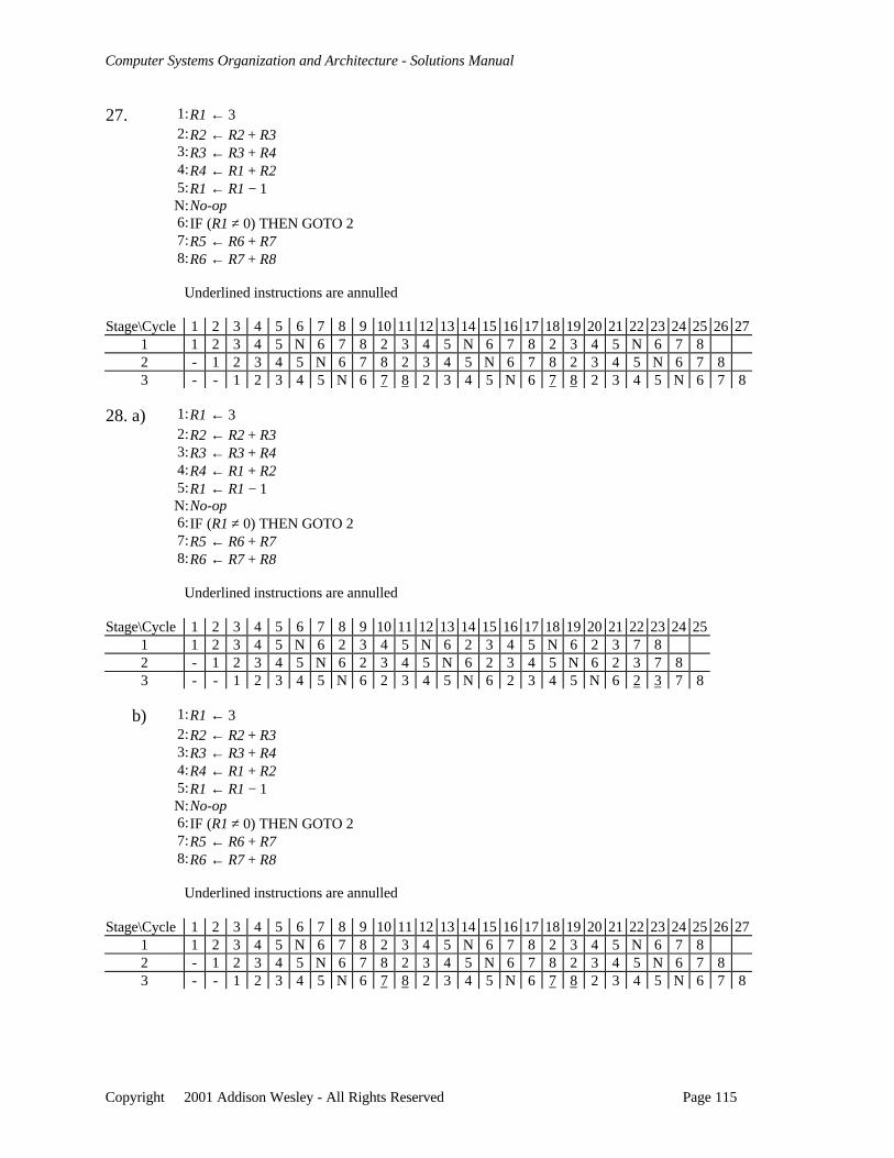
Computer Systems Organization and Architecture - Solutions Manual
Copyright 2001 Addison Wesley - All Rights Reserved Page 115
27. 1:R1 ← 32:R2 ← R2 + R33:R3 ← R3 + R44:R4 ← R1 + R25:R1 ← R1 − 1N:No-op6:IF (R1 ≠ 0) THEN GOTO 27:R5 ← R6 + R78:R6 ← R7 + R8
Underlined instructions are annulled
Stage\Cycle 1 2 3 4 5 6 7 8 9 10 11 12 13 14 15 16 17 18 19 20 21 22 23 24 25 26 271 1 2 3 4 5 N 6 7 8 2 3 4 5 N 6 7 8 2 3 4 5 N 6 7 82 - 1 2 3 4 5 N 6 7 8 2 3 4 5 N 6 7 8 2 3 4 5 N 6 7 83 - - 1 2 3 4 5 N 6 7 8 2 3 4 5 N 6 7 8 2 3 4 5 N 6 7 8
28. a) 1:R1 ← 32:R2 ← R2 + R33:R3 ← R3 + R44:R4 ← R1 + R25:R1 ← R1 − 1N:No-op6:IF (R1 ≠ 0) THEN GOTO 27:R5 ← R6 + R78:R6 ← R7 + R8
Underlined instructions are annulled
Stage\Cycle 1 2 3 4 5 6 7 8 9 10 11 12 13 14 15 16 17 18 19 20 21 22 23 24 251 1 2 3 4 5 N 6 2 3 4 5 N 6 2 3 4 5 N 6 2 3 7 82 - 1 2 3 4 5 N 6 2 3 4 5 N 6 2 3 4 5 N 6 2 3 7 83 - - 1 2 3 4 5 N 6 2 3 4 5 N 6 2 3 4 5 N 6 2 3 7 8
b) 1:R1 ← 32:R2 ← R2 + R33:R3 ← R3 + R44:R4 ← R1 + R25:R1 ← R1 − 1N:No-op6:IF (R1 ≠ 0) THEN GOTO 27:R5 ← R6 + R78:R6 ← R7 + R8
Underlined instructions are annulled
Stage\Cycle 1 2 3 4 5 6 7 8 9 10 11 12 13 14 15 16 17 18 19 20 21 22 23 24 25 26 271 1 2 3 4 5 N 6 7 8 2 3 4 5 N 6 7 8 2 3 4 5 N 6 7 82 - 1 2 3 4 5 N 6 7 8 2 3 4 5 N 6 7 8 2 3 4 5 N 6 7 83 - - 1 2 3 4 5 N 6 7 8 2 3 4 5 N 6 7 8 2 3 4 5 N 6 7 8
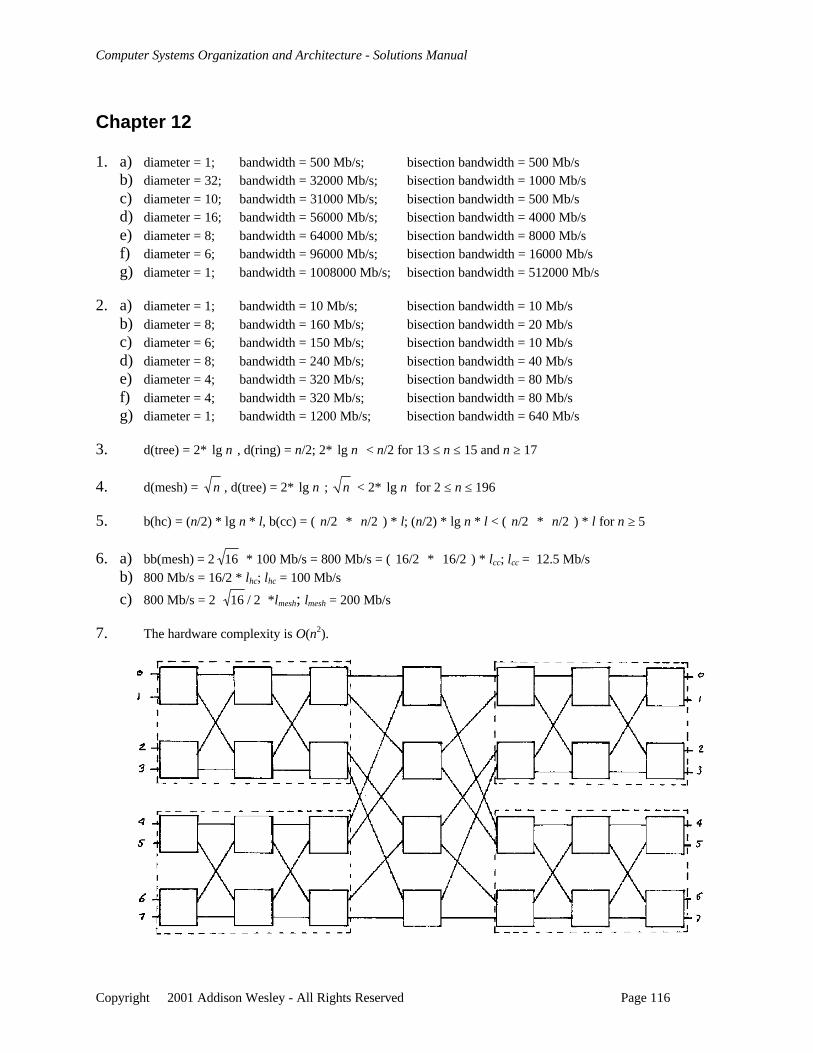
Computer Systems Organization and Architecture - Solutions Manual
Copyright 2001 Addison Wesley - All Rights Reserved Page 116
Chapter 12
1. a) diameter = 1; bandwidth = 500 Mb/s; bisection bandwidth = 500 Mb/sb) diameter = 32; bandwidth = 32000 Mb/s; bisection bandwidth = 1000 Mb/sc) diameter = 10; bandwidth = 31000 Mb/s; bisection bandwidth = 500 Mb/sd) diameter = 16; bandwidth = 56000 Mb/s; bisection bandwidth = 4000 Mb/se) diameter = 8; bandwidth = 64000 Mb/s; bisection bandwidth = 8000 Mb/sf) diameter = 6; bandwidth = 96000 Mb/s; bisection bandwidth = 16000 Mb/sg) diameter = 1; bandwidth = 1008000 Mb/s; bisection bandwidth = 512000 Mb/s
2. a) diameter = 1; bandwidth = 10 Mb/s; bisection bandwidth = 10 Mb/sb) diameter = 8; bandwidth = 160 Mb/s; bisection bandwidth = 20 Mb/sc) diameter = 6; bandwidth = 150 Mb/s; bisection bandwidth = 10 Mb/sd) diameter = 8; bandwidth = 240 Mb/s; bisection bandwidth = 40 Mb/se) diameter = 4; bandwidth = 320 Mb/s; bisection bandwidth = 80 Mb/sf) diameter = 4; bandwidth = 320 Mb/s; bisection bandwidth = 80 Mb/sg) diameter = 1; bandwidth = 1200 Mb/s; bisection bandwidth = 640 Mb/s
3. d(tree) = 2*lg n, d(ring) = n/2; 2*lg n < n/2 for 13 ≤ n ≤ 15 and n ≥ 17
4. d(mesh) = n , d(tree) = 2*lg n; n < 2*lg n for 2 ≤ n ≤ 196
5. b(hc) = (n/2) * lg n * l, b(cc) = (n/2 * n/2) * l; (n/2) * lg n * l < (n/2 * n/2) * l for n ≥ 5
6. a) bb(mesh) = 2 16 * 100 Mb/s = 800 Mb/s = (16/2 * 16/2) * lcc; lcc = 12.5 Mb/sb) 800 Mb/s = 16/2 * lhc; lhc = 100 Mb/s
c) 800 Mb/s = 2 2/16 *lmesh; lmesh = 200 Mb/s
7. The hardware complexity is O(n2).
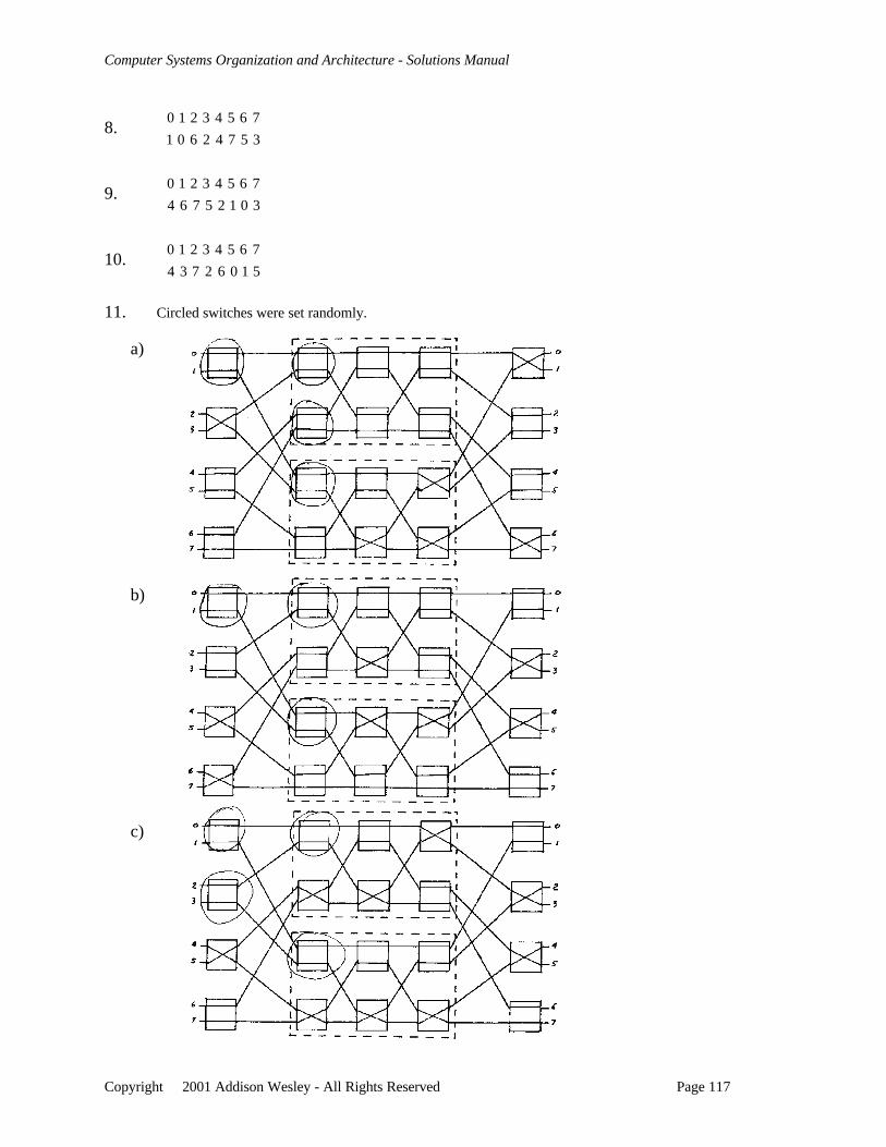
Computer Systems Organization and Architecture - Solutions Manual
Copyright 2001 Addison Wesley - All Rights Reserved Page 117
8.
35742601
76543210
9.
30125764
76543210
10.
51062734
76543210
11. Circled switches were set randomly.
a)
b)
c)
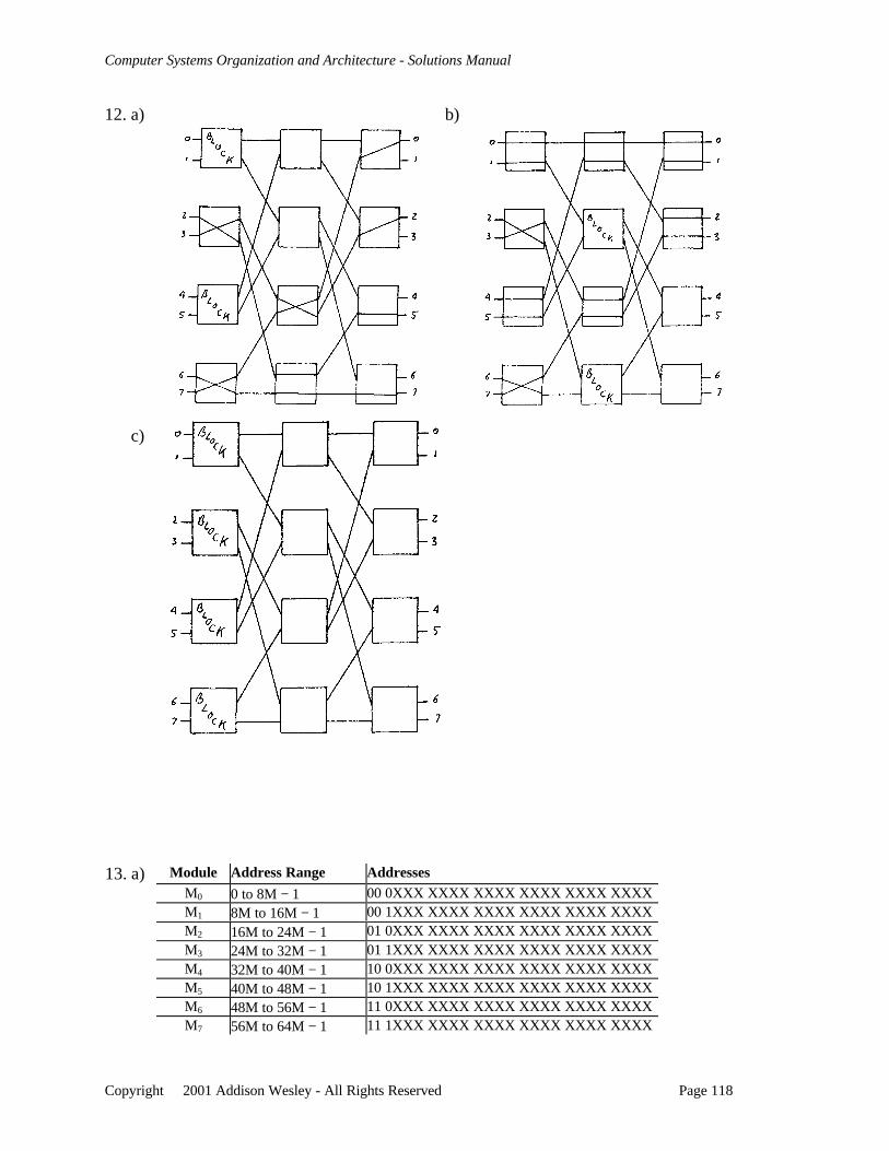
Computer Systems Organization and Architecture - Solutions Manual
Copyright 2001 Addison Wesley - All Rights Reserved Page 118
12. a) b)
c)
13. a) Module Address Range AddressesM0 0 to 8M − 1 00 0XXX XXXX XXXX XXXX XXXX XXXXM1 8M to 16M − 1 00 1XXX XXXX XXXX XXXX XXXX XXXXM2 16M to 24M − 1 01 0XXX XXXX XXXX XXXX XXXX XXXXM3 24M to 32M − 1 01 1XXX XXXX XXXX XXXX XXXX XXXXM4 32M to 40M − 1 10 0XXX XXXX XXXX XXXX XXXX XXXXM5 40M to 48M − 1 10 1XXX XXXX XXXX XXXX XXXX XXXXM6 48M to 56M − 1 11 0XXX XXXX XXXX XXXX XXXX XXXXM7 56M to 64M − 1 11 1XXX XXXX XXXX XXXX XXXX XXXX
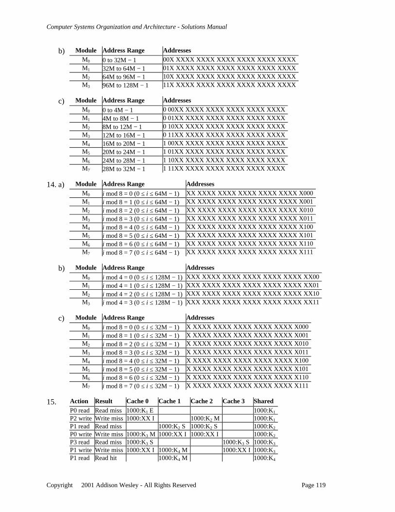
Computer Systems Organization and Architecture - Solutions Manual
Copyright 2001 Addison Wesley - All Rights Reserved Page 119
b) Module Address Range AddressesM0 0 to 32M − 1 00X XXXX XXXX XXXX XXXX XXXX XXXXM1 32M to 64M − 1 01X XXXX XXXX XXXX XXXX XXXX XXXXM2 64M to 96M − 1 10X XXXX XXXX XXXX XXXX XXXX XXXXM3 96M to 128M − 1 11X XXXX XXXX XXXX XXXX XXXX XXXX
c) Module Address Range AddressesM0 0 to 4M − 1 0 00XX XXXX XXXX XXXX XXXX XXXXM1 4M to 8M − 1 0 01XX XXXX XXXX XXXX XXXX XXXXM2 8M to 12M − 1 0 10XX XXXX XXXX XXXX XXXX XXXXM3 12M to 16M − 1 0 11XX XXXX XXXX XXXX XXXX XXXXM4 16M to 20M − 1 1 00XX XXXX XXXX XXXX XXXX XXXXM5 20M to 24M − 1 1 01XX XXXX XXXX XXXX XXXX XXXXM6 24M to 28M − 1 1 10XX XXXX XXXX XXXX XXXX XXXXM7 28M to 32M − 1 1 11XX XXXX XXXX XXXX XXXX XXXX
14. a) Module Address Range AddressesM0 i mod 8 = 0 (0 ≤ i ≤ 64M − 1) XX XXXX XXXX XXXX XXXX XXXX X000M1 i mod 8 = 1 (0 ≤ i ≤ 64M − 1) XX XXXX XXXX XXXX XXXX XXXX X001M2 i mod 8 = 2 (0 ≤ i ≤ 64M − 1) XX XXXX XXXX XXXX XXXX XXXX X010M3 i mod 8 = 3 (0 ≤ i ≤ 64M − 1) XX XXXX XXXX XXXX XXXX XXXX X011M4 i mod 8 = 4 (0 ≤ i ≤ 64M − 1) XX XXXX XXXX XXXX XXXX XXXX X100M5 i mod 8 = 5 (0 ≤ i ≤ 64M − 1) XX XXXX XXXX XXXX XXXX XXXX X101M6 i mod 8 = 6 (0 ≤ i ≤ 64M − 1) XX XXXX XXXX XXXX XXXX XXXX X110M7 i mod 8 = 7 (0 ≤ i ≤ 64M − 1) XX XXXX XXXX XXXX XXXX XXXX X111
b) Module Address Range AddressesM0 i mod 4 = 0 (0 ≤ i ≤ 128M − 1) XXX XXXX XXXX XXXX XXXX XXXX XX00M1 i mod 4 = 1 (0 ≤ i ≤ 128M − 1) XXX XXXX XXXX XXXX XXXX XXXX XX01M2 i mod 4 = 2 (0 ≤ i ≤ 128M − 1) XXX XXXX XXXX XXXX XXXX XXXX XX10M3 i mod 4 = 3 (0 ≤ i ≤ 128M − 1) XXX XXXX XXXX XXXX XXXX XXXX XX11
c) Module Address Range AddressesM0 i mod 8 = 0 (0 ≤ i ≤ 32M − 1) X XXXX XXXX XXXX XXXX XXXX X000M1 i mod 8 = 1 (0 ≤ i ≤ 32M − 1) X XXXX XXXX XXXX XXXX XXXX X001M2 i mod 8 = 2 (0 ≤ i ≤ 32M − 1) X XXXX XXXX XXXX XXXX XXXX X010M3 i mod 8 = 3 (0 ≤ i ≤ 32M − 1) X XXXX XXXX XXXX XXXX XXXX X011M4 i mod 8 = 4 (0 ≤ i ≤ 32M − 1) X XXXX XXXX XXXX XXXX XXXX X100M5 i mod 8 = 5 (0 ≤ i ≤ 32M − 1) X XXXX XXXX XXXX XXXX XXXX X101M6 i mod 8 = 6 (0 ≤ i ≤ 32M − 1) X XXXX XXXX XXXX XXXX XXXX X110M7 i mod 8 = 7 (0 ≤ i ≤ 32M − 1) X XXXX XXXX XXXX XXXX XXXX X111
15. Action Result Cache 0 Cache 1 Cache 2 Cache 3 SharedP0 read Read miss 1000:K1 E 1000:K1
P2 write Write miss 1000:XX I 1000:K2 M 1000:K1
P1 read Read miss 1000:K2 S 1000:K2 S 1000:K2
P0 write Write miss 1000:K3 M 1000:XX I 1000:XX I 1000:K2
P3 read Read miss 1000:K3 S 1000:K3 S 1000:K3
P1 write Write miss 1000:XX I 1000:K4 M 1000:XX I 1000:K3
P1 read Read hit 1000:K4 M 1000:K4
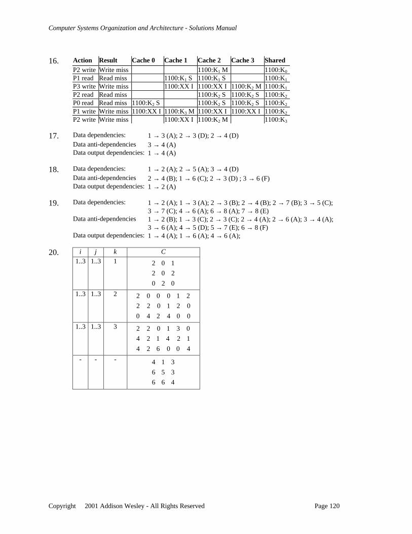
Computer Systems Organization and Architecture - Solutions Manual
Copyright 2001 Addison Wesley - All Rights Reserved Page 120
16. Action Result Cache 0 Cache 1 Cache 2 Cache 3 SharedP2 write Write miss 1100:K1 M 1100:K0
P1 read Read miss 1100:K1 S 1100:K1 S 1100:K1
P3 write Write miss 1100:XX I 1100:XX I 1100:K2 M 1100:K1
P2 read Read miss 1100:K2 S 1100:K2 S 1100:K2
P0 read Read miss 1100:K2 S 1100:K2 S 1100:K2 S 1100:K2
P1 write Write miss 1100:XX I 1100:K3 M 1100:XX I 1100:XX I 1100:K2
P2 write Write miss 1100:XX I 1100:K2 M 1100:K3
17. Data dependencies: 1 → 3 (A); 2 → 3 (D); 2 → 4 (D)Data anti-dependencies 3 → 4 (A)Data output dependencies: 1 → 4 (A)
18. Data dependencies: 1 → 2 (A); 2 → 5 (A); 3 → 4 (D)Data anti-dependencies 2 → 4 (B); 1 → 6 (C); 2 → 3 (D) ; 3 → 6 (F)Data output dependencies: 1 → 2 (A)
19. Data dependencies: 1 → 2 (A); 1 → 3 (A); 2 → 3 (B); 2 → 4 (B); 2 → 7 (B); 3 → 5 (C);3 → 7 (C); 4 → 6 (A); 6 → 8 (A); 7 → 8 (E)
Data anti-dependencies 1 → 2 (B); 1 → 3 (C); 2 → 3 (C); 2 → 4 (A); 2 → 6 (A); 3 → 4 (A);3 → 6 (A); 4 → 5 (D); 5 → 7 (E); 6 → 8 (F)
Data output dependencies: 1 → 4 (A); 1 → 6 (A); 4 → 6 (A);
20. i j k C
1..3 1..3 1
020
202
102
1..3 1..3 2
+++++++++
004240
021022
210002
1..3 1..3 3
+++++++++
400624
124124
031022
- - -
466
356
314
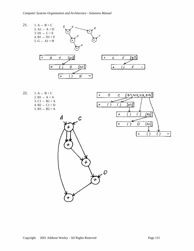
Computer Systems Organization and Architecture - Solutions Manual
Copyright 2001 Addison Wesley - All Rights Reserved Page 121
21. 1. A ← B + C2. A1 ← A + D3. D1 ← C + E4. B1 ← D1 + F5. G ← A1 + H
22. 1. A ← B + C2. B1 ← A + A3. C1 ← B1 + A4. B2 ← C1 + D5. B3 ← B2 + A