Embed Size (px)
Citation preview
CONDUCTIVE POLYMER NANOCOMPOSITES OF POLYPROPYLENE
AND ORGANIC FIELD EFFECT TRANSISTORS WITH POLYETHYLENE
GATE DIELECTRIC
A THESIS SUBMITTED TO
THE GRADUATE SCHOOL OF NATURAL AND APPLIED SCIENCES
OF
MIDDLE EAST TECHNICAL UNIVERSITY
BY
YASİN KANBUR
IN PARTIAL FULFILLMENT OF THE REQUIREMENTS
FOR
THE DEGREE OF DOCTOR OF PHILOSOPHY
IN
POLYMER SCIENCE AND TECHNOLOGY
JUNE 2011
ii
Approval of the thesis:
CONDUCTIVE POLYMER NANOCOMPOSITES OF POLYPROPYLENE
AND ORGANIC FIELD EFFECT TRANSISTORS WITH POLYETHYLENE
GATE DIELECTRIC
Submitted by YASİN KANBUR in partial fulfillment of the requirements for the
degree of Doctor of Philosophy in Polymer Science and Technology, Middle East
Technical University by,
Prof. Dr. Canan Özgen _________________
Dean, Graduate School of Natural and Applied Sciences
Prof. Dr. Necati Özkan _________________
Head of Department, Polymer Science and Technology
Prof. Dr. Zuhal Küçükyavuz
Supervisor, Chemistry Dept., METU _________________
Examining Committee Members:
Prof. Dr. Erdal Bayramlı
Chemistry Dept., METU _________________
Prof. Dr. Zuhal Küçükyavuz
Chemistry Dept., METU _________________
Prof. Dr. Göknur Bayram
Chemical Engineering Dept., METU ________________
Assist. Prof. Dr. Nurdan Sankır
Micro and Nanotechnology Dept., TOBB-ETU ________________
Assist. Prof. Dr. Ali Çırpan
Chemistry Dept., METU _______________
Date: June 15, 2011
iii
I hereby declare that all information in this document has been obtained and
presented in accordance with academic rules and ethical conduct. I also declare
that, as required by these rules and conduct, I have fully cited and referenced
all material and results that are not original to this work.
Name, Last name: YASİN KANBUR
Signature :
iv
ABSTRACT
CONDUCTIVE POLYMER NANOCOMPOSITES OF POLYPROPYLENE AND
ORGANIC FIELD EFFECT TRANSISTORS WITH POLYETHYLENE GATE
DIELECTRIC
KANBUR, Yasin
Ph. D., Department of Polymer Science and Technology
Supervisor: Prof. Dr. Zuhal KÜÇÜKYAVUZ
June 2011, 124 pages
One of the aim of this study is to prepare conductive polymer nanocomposites of
polypropylene to obtain better mechanical and electrical properties. Composite
materials based on conductive fillers dispersed within insulating thermoplastic
matrices have wide range of application. For this purpose, conductive polymer
nanocomposites of polypropylene with nano dimentional conductive fillers like
carbon black, carbon nanotube and fullerene were prepared. Their mechanical,
electrical and thermal properties were investigated.
Polypropylene (PP)/carbon black (CB) composites at different compositions were
prepared via melt blending of PP with CB. The effect of CB content on mechanical
and electrical properties was studied. Test samples were prepared by injection
molding and compression molding techniques. Also, the effect of processing type on
mechanical and electrical properties was investigated. Composites become
semiconductive with the addition of 2 wt% CB.
v
Polypropylene (PP) / Carbon Nanotube (CNT) and Polypropylene / Fullerene
composites were prepared by melt mixing. CNT‟s and fullerenes were surface
functionalized with HNO3 : H2SO4 before composite preparation. The CNT and
fullerene content in the composites were varied as 0.5, 1.0, 2.0 and 3.0 % by weight.
For the composites which contain surface modified CNT and fullerene four different
compatibilizers were used. These were selected as TritonX-100, Poly(ethylene-
block-polyethylene glycol), Maleic anhydride grafted Polypropylene and Cetramium
Bromide. The effect of surface functionalization and different compatibilizer on
mechanical, thermal and electrical properties were investigated. Best value of these
properties were observed for the composites which were prepared with maleic
anhydride grafted polypropylene and cetramium bromide.
Another aim of this study is to built and characterize transistors which have
polyethylene as dielectric layers. While doing this, polyethylene layer was deposited
on gate electrode using vacuum evaporation system. Fullerene , Pentacene ve Indigo
were used as semiconductor layer. Transistors work with low voltage and high on/off
ratio were built with Aluminum oxide - PE and PE dielectrics.
Keywords: Conductive Polymer Composites, Nanocomposites, Mechanical
Properties, Electrical Properties, Organic Field Effect Transistors
vi
ÖZ
POLİPROPİLEN İLETKEN NANOKOMPOZİTLERİ VE POLİETİLEN KAPI
DİLEKTRİKLİ ORGANİK ALAN ETKİLİ TRANSİSTÖRLER
KANBUR, Yasin
Doktora, Polimer Bilim ve Teknolojisi
Tez Yöneticisi: Prof. Dr. Zuhal KÜÇÜKYAVUZ
Mayıs 2011, 124 sayfa
Bu çalışmanın amaçlarından biri daha iyi mekanik ve elektiriksel özellikler elde
etmek için iletken polipropilen nanokompozitleri hazırlamaktır. Termoplastik
yalıtkan matrisler içerisinde iletken dolgu malzemelerinin dağılımına dayalı
kompozit malzemeler geniş bir kullanım alanına sahiptir. Bu amaçla, polipropilenin
karbon siyahı, karbon nanotüp ve fulleren gibi nano boyutlu iletken dolgu
malzemeleri içeren nanokompozitleri hazırlandı. Kompozitlerin mekanik, elektiriksel
ve termal özellikleri incelendi.
Polipropilen/Karbon Siyahı kompozitleri farklı bileşimlerde eriyik karıştırma
yöntemiyle hazırlandı. Karbon siyahı miktarının mekanik ve elektiriksel özellikler
üzerindeki etkisi araştırıldı. Test örnekleri enjeksiyonlu kalıplama ve basınçlı
kalıplama teknikleri ile hazırlandı. Ayrıca proses tipinin mekanik ve elektiriksel
özelliklere olan etkisi incelendi. Kompoziler 2 % karbon siyahı eklenmesi ile yarı
iletken hale geldiler.
Polipropilen / Karbon Nanotüp ve Polipropilen / Fulleren kompozitleri eriyik
karıştırma yöntemiyle hazırlandı. Kompozitlerin hazırlanmasından önce karbon
vii
nanotüp ve fullerenin yüzeyi HNO3 : H2SO4 ile fonksiyonlandırıldı. Kompozitlerdeki
karbon nanotüp ve fulleren kompozisyonu ağırlık yüzdesi olarak 0.5, 1.0, 2.0 ve 3.0
% olarak değiştirildi. Yüzeyi modifiye edilmiş karbon nanotüp ve fulleren içeren
kompozitlerde dört farklı uyumlaştırıcı kullanıldı. Bunlar, TritonX-100, Poli(etilen-
blok-polietilen glikol), Maleik anhidrit graft edilmiş Polipropilen ve Setramiyum
Bromür olarak seçildi. Yüzey modifikasyonu ve farklı uyumlaştırıcıların mekanik,
termal ve elektiriksel özellikler üzerine olan etkisi incelendi. Bu özelliklerin en iyi
değerleri maleik anhidrit graft edilmiş polipropilen ve setramiyum bromür ile
hazırlanan kompozitlerde gözlemlendi.
Bu çalışmanın başka bir amacı polietilen dielektrik tabakası içeren transistörler
yapmak ve karakterize etmektir. Bunu yaparken polietilen tabakasının
oluşturulmasında vakumla buharlaştırma sistemi kullanıldı. Fulleren, Pentasen ve
Indigo yarı iletken tabaka olarak kullanıldı. Aluminyum oksit -PE veya PE dielektrik
tabakalarına sahip düşük voltajda çalışan ve yüksek açma kapama oranına sahip
transistörler elde edildi.
Anahtar Sözcükler: İletken Polimer Kompozitleri, Nanokompozitler, Mekanik
Özellikler, Elektriksel Özellikler, Organik Alan Etkili Transitörler

viii
To My wife Seyhan and my son Eren

ix
ACKNOWLEDGMENTS
I express my gratitude to my supervisor Prof. Dr. Zuhal Küçükyavuz for her
guidance and excellent helps during this work. I also would like to thank her for not
only her support throughout my PhD but also treated me like a son.
I would like to thank to Prof. Dr. Erdal Bayramlı and Göknur Bayram for their
excellent help, guidance and support.
I am much indebted to Prof. Dr. N. Serdar Sarıçiftçi for his excellent help, guidance
and support during my study in Linz, Austria. During 6 months in Linz, he always
gave inspiration and encouragement to me.
Special thanks to Dr. Mihai Irimia Vladu who taught me a lot about organic field
effect transistors.
I wish to thank to Dr. Mamatimin Abbas, Dr. Philip Stadler, Dr. Martin Egginger,
Dr. Anita Fuchsbauer, Melanie Reisinger, Erik Glowacki, Sandra Kogler, Stefan
Schauer, Serpil Tekoğlu, Ercan Avcı, for their help, hospitality and friendship during
my stay in Linz.
My deepest thanks are to my wife Seyhan Kanbur and all of the my family members
for loving me.
I would like to express my endless thanks to all my labmates, Çetin Börüban, Sevil
Baytekin, Feride Tezal, Faris Yılmaz, Tamer Tezel, Bahadır Doğan for their supports
and being a part of my life.
x
I am indepted to Assoc.Prof.Dr. Murat Kanbur and Dr. Özlem Usluer, for their
meaningfull advices.
I would like to extend special thanks to Osman Yaslıtaş for his technical supports.
I offer sincere thanks to my friends, Yasin Arslan, Mehmet Doğan, Ali Sinan Dike,
Ümit Tayfun, Selahattin Erdoğan, Fuat Çankaya, Ufuk Abacı, Elif Vargün, Arzu
Yavuz, Tugba Efe, Yusuf Nur, Selin Kozanoglu, Buket Çarbaş, Murat Güzel for
everything they have done for me.
I also wish to thank to my colleagues in Chemistry Department of METU.
I would like to thank to my PhD exam committee members for spending their time
and interesting in my PhD.
This work was financially supported by ÖYP (Faculty Development Program) from
the Middle East Technical University.
I would like to extend my deepest thanks to Atatürk University for supporting me to
complete my PhD in the chemistry department of METU.
xi
TABLE OF CONTENTS
ABSTRACT…………………………………………………………………… iv
ÖZ……………………………………………………………………………… vi
ACKNOWLEDGEMENTS…………………………………………………… ix
TABLE OF CONTENTS………………………………….…………………... xi
LIST OF TABLES…………………………………………………….……...... xv
LIST OF FIGURES………………………….………………………………… xvi
ABBREVATIONS…………………………………………………………….. xxi
CHAPTERS….…………………………………………………………………
1. INTRODUCTION.………………………………………………………….. 1
2. BACKROUND INFORMATION………………….……………………..... 3
2.1 Polymer Matrice for Composite Preparation…………..…………...…… 3
2.1.2 Polypropylene…………...…………. ……………………………… 3
2.2 Polymer Dielectric for Organic Field Effect Transistor…..………..….. 5
2.2.1 Polyethylene…..……………………………………………………. 5
2.3 Conductive Fillers……………..………………………………………... 6
2.3.1 Carbon Nanotubes……..………………………………………........ 6
2.3.2 Carbon Black…………..……………….…………………………... 10
2.3.3 Fullerene……..………………..……………………………………. 12
2.4 Composites and Nanocomposites..…………………………………….... 13
2.5 Conductive Polymer Composites…………..………..………………...... 14
2.6 Band Theory….……………………………..………………………....... 15
2.7 Principles of Organic Field Effect Transistors…………..……………… 16
2.7.1 Device Structures for OFET Application.…………..…...…………. 18
2.7.2 Characterization of OFET‟s……………..…………………………. 19
2.7.3 Importance of Gate Dielectric for OFET‟s…...…………………..… 20
2.7.4 Techniques for OFET Preparation……………….………………… 22
xii
3. EXPERIMENTAL………………………………………………………....... 24
3.1. Surface Modification of Carbon nanotube with HNO3/H2SO4………… 24
3.2. Surface Modification of Fullerene with HNO3/H2SO4………................. 26
3.3 Composite Preparation……………..……………………….................... 27
3.3.1 Preparation of Polypropylene / CNT composites…………………... 27
3.3.2 Preparation of Polypropylene / Fullerene composites……………… 28
3.3.3. Preparation of Polypropylene /Carbon Black Composites………… 28
3.4 Injection Molding…………... ………………………………………….. 29
3.5 Compression Molding…..……………………………..………………... 30
3.6 Conductivity Measurements……………….……………………………. 30
3.7 Thermal Gravimetric Analysis……………………………..…………… 31
3.8 Fourier Transform Infrared Spectrometer (FTIR)………………………. 31
3.9. Differential Scanning Calorimetry………………………………..……. 32
3.10 Scanning Electron Microscopy (SEM)……………………...…………. 32
3.11 X Ray Photoelectron Spectroscopy (XPS)………………………..…… 32
3.12 Zeta Potential…………………….…………………………………….. 32
3.13 Transmission Electron Microscopy ……………………………...……. 33
3.14 Tensile Test………………………..………………..…………………. 33
3.15 Impact Test……………………...……………………………………... 33
3.16 Melt Flow Index………………..…..………………………………….. 33
3.17 Organic Field Effect Transistor Preparation ………………………….. 34
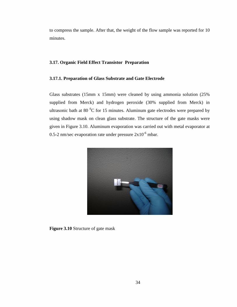
3.17.1 Preparation of Glass Substrate and Gate Electrode…………..…… 34
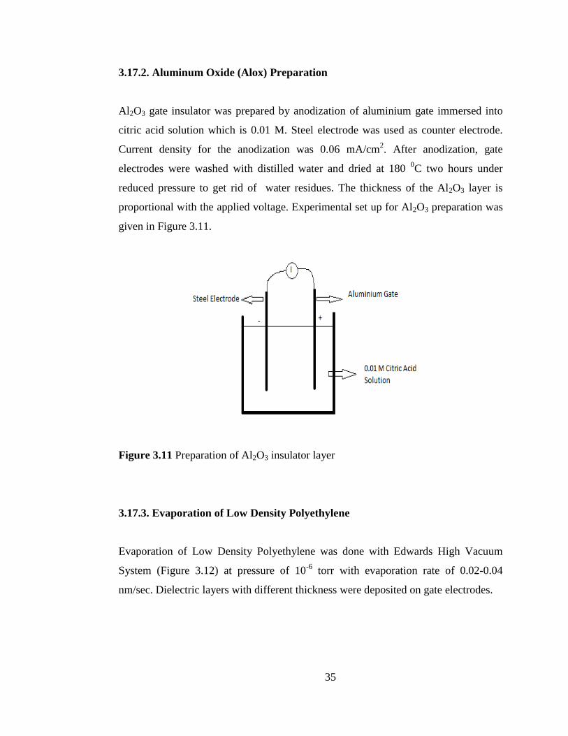
3.17.2 Alox Preparation……..…………………………………………… 35
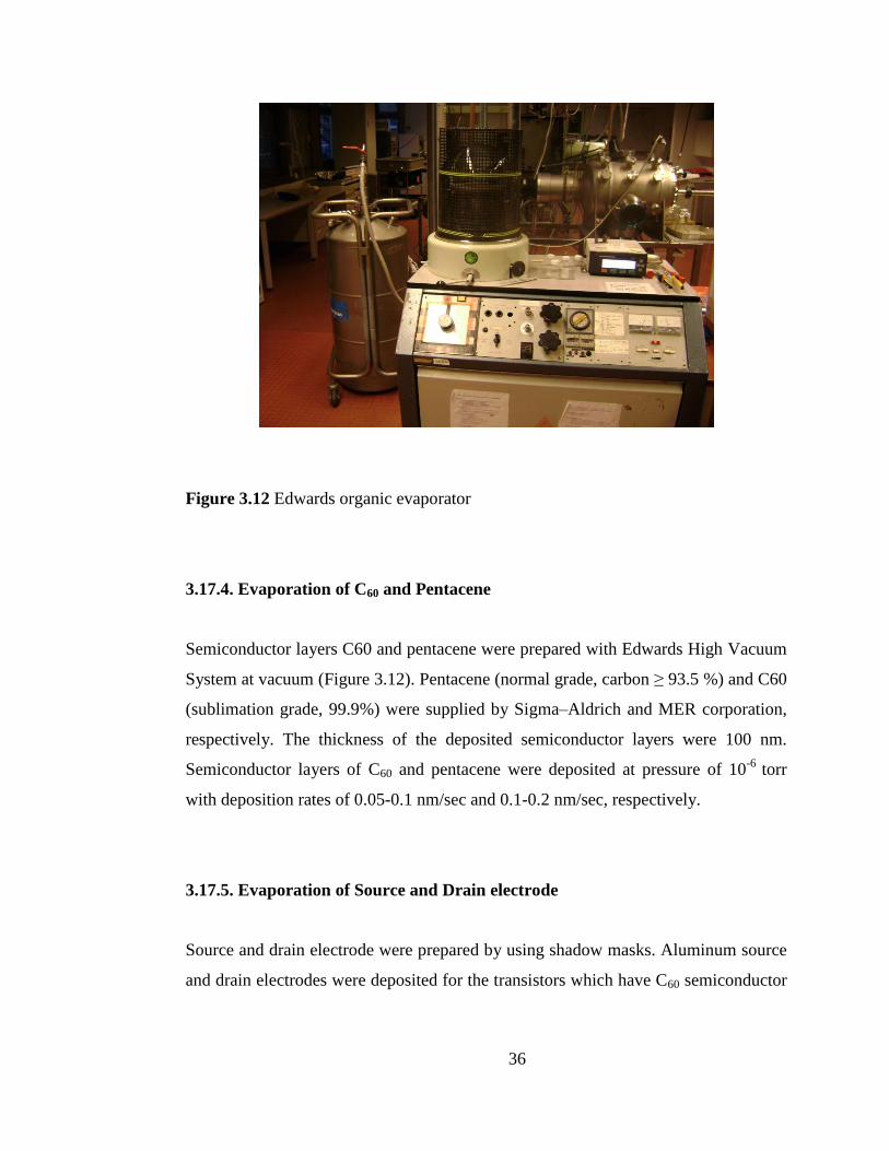
3.17.3 Evaporation of Low Density Polyethylene……...………………... 35
3.17.4 Evaporation of C60 and Pentacene ……………………………….. 36
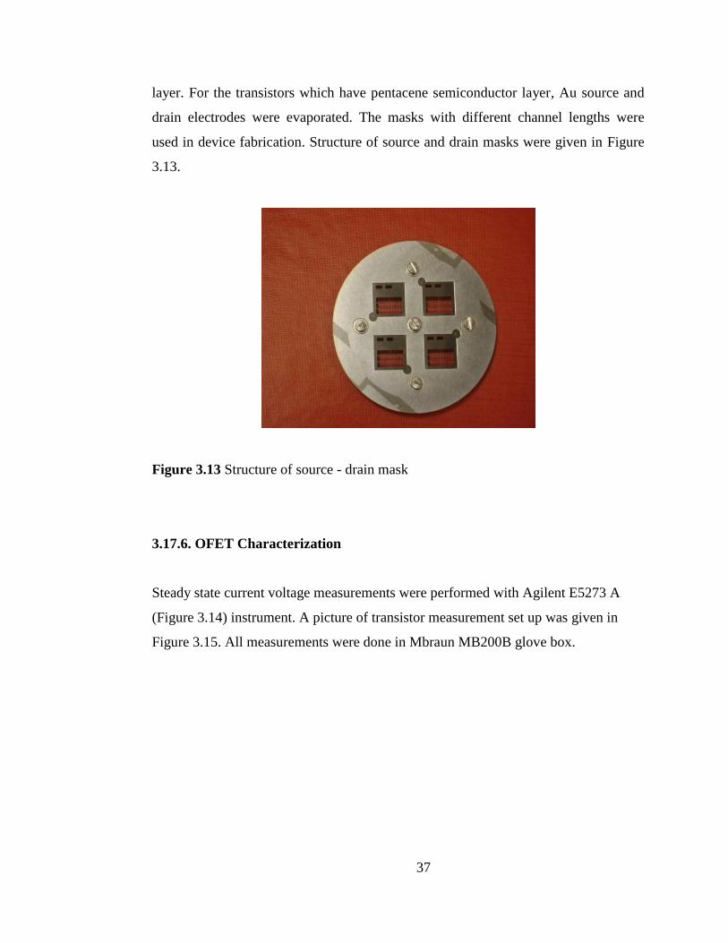
3.17.5 Evaporation of Source and Drain electrode ……………….……... 36
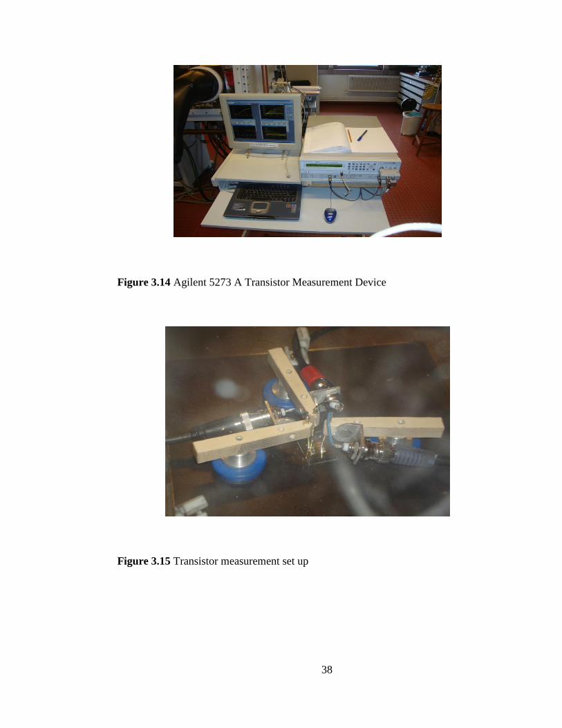
3.17.6 OFET Characterization……..…………………………………….. 37
3.17.7 Dielectric Characterization…....…..…….………………………… 39
4. RESULTS AND DISCUSSION……………..……………………………… 41
4.1 Polypropylene / Carbon Black Composites……………………….…….. 41
xiii
4.1.1 Melt Flow Index ……..…………………….……………………… 41
4.1.2 Percent Crystallinity of PP/CB composites…………………...….… 42
4.1.3 Impact Test………………………..……………………….…….…. 43
4.1.4 Scanning Electron Microscopy (SEM)……………………..…........ 44
4.1.5 Mechanical Properties …...……………………..…………..……… 47
4.1.6 Electrical Properties ……..…………………………………..…….. 49
4.1.7 Thermal Gravimetric Analysis (TGA)……………………………... 52
4.2 Surface Modification of Carbon Nanotube.……………………………. 53
4.2.1 Fourier Transform Infrared Spectroscopy (FTIR)..………………... 53
4.2.2 Elemental Analysis….…………………..…...................................... 54
4.2.3 Electrical Conductivity.……………………………..……………… 55
4.2.4 X Ray Photoelectron Spectroscopy (XPS).………….………...…… 55
4.2.5 Zeta Potential ………………………………...…………………….. 57
4.2.6 Scanning Electron Microscopy.……………………………..……... 58
4.2.7 Transmission Electron Microscopy (TEM).…………………...…… 60
4.3 Surface Modification of Fullerene ………………………...………........ 61
4.3.1 Fourier Transform Infrared Spectroscopy (FTIR) ……………….... 61
4.3.2 X Ray Photoelectron Spectroscopy (XPS)………………………… 62
4.3.3 Elemental Analysis……………………………..…………………... 63
4.3.4 Electrical Conductivity …………………………..………………… 64
4.3.5 Transmission Electron Microscopy ……...………………………… 64
4.3.6 Zeta Potential ………………………………………......................... 66
4.3.7 Scanning Electron Microscopy ……………………………………. 66
4.4 Polypropylene/ Carbon Nanotube Composites…………………………. 68
4.4.1 Mechanical Properties …….……………………………………….. 68
4.4.2 Electrical Conductivity ……..……………………………………… 72
4.4.3 Scanning Electron Microscopy (SEM)…………………………….. 73
4.4.4 Thermal Gravimetric Analysis (TGA)……………………………... 77
4.5 Polypropylene /Fullerene Composites ………………………………….. 78
4.5.1 Mechanical Properties …….……………………………………….. 78
xiv
4.5.2 Electrical Conductivity……………………………………………... 82
4.5.3 Scanning Electron Microscopy…………………………………….. 83
4.5.4 Thermal Gravimetric Analysis (TGA)……………………………... 87
4.6 Organic Field Effect Transistors with Polyethylene Gate Dielectric…… 88
4.6.1 Fourier Transform Infrared Spectroscopy…..…………………….... 88
4.6.2 Atomic Force Microscopy………………………………………….. 90
4.6.3 Dielectric Properties…............................…………………………... 91
4.6.4 Characterization of OFET‟s………………………………………... 92
5. CONCLUSIONS……………………………………………………………. 98
5.1 Polypropylene / Carbon Black Composites………………………………... 98
5.2 Surface Modification of Carbon Nanotube …………….............................. 98
5.3 Surface Modification of Fullerene ………………………………………… 99
5.4 Polypropylene/ Carbon Nanotube Composites…………………………….. 99
5.5 Polypropylene / Fullerene Composites ……………………………………. 100
5.6 Organic Field Effect Transistors with Polyethylene Gate Dielectric ……… 100
REFERENCES………………………………………………………………… 101
APPENDICES…………………………………………………………………. 113
A. STRESS AT BREAK OF THE POLYPROPYLENE / CARBON
NANOTUBE AND POLYPROPYLENE / FULLERENE COMPOSITES...
113
B. STRESS VS STRAIN CURVES FOR POLYPROPYLENE / CARBON
NANOTUBE AND POLYPROPYLENE / FULLERENE COMPOSITES..
115
CURRICULUM VITAE……………………………………………………….. 122
xv
LIST OF TABLES
TABLES
Table 4. 1 Elemental analysis results of CN 1 and CN 2……………...……... 54
Table 4. 2 Electrical conductivity of Untreated CN, CN 1 and CN 2…….…. 55
Table 4. 3 Elemental analysis results of surface modified fullerenes ……….. 63
Table 4. 4 Electrical Conductivity of the F1 and F2………….……………… 64
Table 4. 5 Observed peaks and literature-reported peaks for polyethylene.…. 89
xvi
LIST OF FIGURES
FIGURES
Figure 2. 1 Synthesis of Polypropylene………………………...…………….. 3
Figure 2. 2 Structure of Isotactic, Syndiotactic and Atactic Polypropylene…. 4
Figure 2. 3 Structure of Polyethylene ………………………...……….……... 5
Figure 2. 4 Structures of HDPE, LLDPE and LDPE ………………………... 5
Figure 2. 5 Structure of graphite sheet ………………………...…………….. 7
Figure 2. 6 Structure of Multi walled carbon nanotube and Single walled
carbon nanotube................................................................................................
7
Figure 2. 7 Structural isomers of Carbon Nanotubes, armchair (top) zig zag
(middle), chiral(bottom)…..………………………………………………….
8
Figure 2. 8 Agglomerate and Aggregate sizes of Carbon Black..……...…….. 10
Figure 2. 9 Structures of Diamond, Graphite and Carbon Black …………… 11
Figure 2. 10 Structure of C60 ……………………………….…...…………... 12
Figure 2. 11 Structures of some conjugated polymers ……………...……….. 15
Figure 2. 12 Energy Levels of Insulator, Semiconductor and Conductor…… 16
Figure 2. 13 Structure of an OFET ………………………...………………... 16
Figure 2. 14 Working Principle of an OFET …………..……...…………….. 18
Figure 2. 15 Different built structures for OFET‟s : a) bottom-gate bottom-
contact, b) bottom gate top-contact, c) top-gate bottom-contact, d) top-gate
top-contact ………………………..…………………….................................
19
Figure 2. 16 Typical transfer curve for an OFET ………………….....……… 20
Figure 2. 17 Typical output curve for an OFET ………………………...…… 20
Figure 3. 1 Experimental set up for surface modification……………………. 25
Figure 3. 2 Chemical structure of the chemically modified carbon nanotube.. 25
xvii
Figure 3. 3 Reaction of Fullerene with HHO3/H2SO4………………….......... 26
Figure 3. 4 DSM Explore Microcompounder………………………………... 27
Figure 3. 5 Brabender PLV-151 Plasticorder……………………………..…. 28
Figure 3. 6 Daca Injection Molding Instrument……………………………… 29
Figure 3. 7 Dimension of the injection molded test samples………………… 29
Figure 3. 8 Dimension of the compression molded samples……………….... 30
Figure 3. 9 Four point probe technique ………………………………….….. 31
Figure 3. 10 Structure of gate mask………………………………………….. 34
Figure 3. 11 Preparation of Al2O3 insulator layer…………………………… 35
Figure 3. 12 Edwards organic evaporator……………………………………. 36
Figure 3. 13 Structure of source- drain mask………………………………… 37
Figure 3. 14 Agilent 5273 A Transistor Measurement Device………………. 38
Figure 3. 15 Transistor measurement set up…………………………………. 38
Figure 3. 16 Mbraun MB200B Glove box…………………………………… 39
Figure 3. 17 Novocontrol dielectric characterization equipment…………….. 40
Figure 3. 18 MIM structure for dielectric measurements…………………….. 40
Figure 4. 1 Melt flow properties of PP/CB composites ……………………... 42
Figure 4.2 Percent crystallinity of the PP/CB composites…………………… 43
Figure 4. 3 Impact test results for PP/CB composites ………………….......... 44
Figure 4. 4. a Fracture surface of Pure Polypropylene ……………………… 45
Figure 4. 4.b Fracture surface of the PP/CB composites containing 5% CB… 45
Figure 4. 4.c Fracture surface of the PP/CB composites containing 15% CB. 46
Figure 4.4.d Fracture surface of the PP/CB composites containing 30% CB. 46
Figure 4. 5 Tensile Strength of PP/CB composites …………………….......... 47
Figure 4. 6 Young Modulus of PP/CB composites…………………………... 48
Figure 4.7 Percent elongation at break of the PP/CB composites……………. 49
Figure 4.8 Electrical conductivity of the PP/CB composites prepared by
compression and injection molding ……………………………………….….
50
Figure 4.9 The relationship between electrical conductivity and percent
elongation at break as a function of carbon black content for composites
51
xviii
prepared by compression molding …………………………………………...
Figure 4.10 The relationship between electrical conductivity and percent
elongation at break as a function of carbon black content for composites
prepared by injection molding………………………………………………...
52
Figure 4. 11 TGA of the PP/CB composites.……………..………………….. 53
Figure 4. 12 FTIR spectrums of CN 1 and CN 2…………………………… 54
Figure 4. 13 XPS spectra of the CN 1 ………………………………………. 56
Figure 4. 14 XPS spectra of the CN 2……………………………………….. 57
Figure 4. 15 SEM micrograph of untreated CN ……………………………... 58
Figure 4. 16 SEM micrograph of untreated CN 1 …………………………… 59
Figure 4. 17 SEM micrograph of untreated CN 2……………………............. 59
Figure 4. 18 TEM micrograph of CN 1………………………………………. 60
Figure 4. 19 TEM micrograph of CN 2……………………………………… 60
Figure 4. 20 FTIR spectrum of F 1 and F 2………………………………….. 61
Figure 4. 21 XPS spectrum of F1 …………………………………………. 62
Figure 4. 22 XPS spectrum of F 2…………………………………………. 63
Figure 4. 23 TEM micrograph of neat fullerene ………………………….... 65
Figure 4. 24 TEM micrograph of F1 ………………………………………… 65
Figure 4. 25 TEM micrograph of F2…………………………………………. 65
Figure 4. 26 SEM micrograph of neat fullerene ……………………………... 67
Figure 4. 27 SEM micrograph of F1 ………………………………………... 67
Figure 4. 28 SEM micrograph of F2 ………………………………………… 68
Figure 4. 29 Young‟s Modulus of PP/CNT composites …………………….. 70
Figure 4. 30 Percent elongation at break of PP/CNT composites ………….... 71
Figure 4. 31 Electrical Conductivity of the PP/CNT composites …………… 73
Figure 4. 32.a SEM micrograph of PP/m-CNT/ CTAB …………………..… 74
Figure 4. 32.b SEM micrograph of PP/m-CNT/ MA-g-PP ……………….… 75
Figure 4. 32.c SEM micrograph of PP / m-CNT ……………………………. 75
Figure 4. 32.d SEM micrograph of PP / neat CNT…………………………. 76
Figure 4. 32.e SEM micrograph of PP / m-CNT / Triton X-100.…………… 76
xix
Figure 4. 32.f SEM micrograph of PP / m-CNT/ PE-block- PEG ……….… 77
Figure 4. 33 TGA of the PP/CNT composites …………………………...….. 78
Figure 4. 34 Young‟s Modulus of PP/F composites …….…………….…….. 80
Figure 4.35 Percent elongation at break of PP/F composites ……………….. 81
Figure 4. 36 Electrical Conductivity of the PP/F composites …………......… 83
Figure 4. 37.a SEM micrograph of PP / neat F……………………………… 84
Figure 4. 37.b SEM micrograph of PP / m-F ……………………………….. 85
Figure 4. 37.c SEM micrograph of PP/m-F/ CTAB…………………………. 85
Figure 4. 37.d SEM micrograph of PP/m-F/ MA-g-PP …………………….. 86
Figure 4. 37.e SEM micrograph of PP / m-F / Triton X-100 ……………….. 86
Figure 4. 37.f SEM micrograph of PP / m-F/ PE-block- PEG……………… 87
Figure 4. 38. TGA of the PP/F composites……………………….………….. 88
Figure 4.39 FTIR Spectrum of vacuum evaporated polyethylene……….…... 89
Figure 4.40 Atomic force microscopy of vacuum-processed polyethylene on
aluminum oxide gate dielectric showing island formation and growing of the
film: a)10 nm thick film; b) 10 nm thick film annealed at 100C for 15 min;
c) 20 nm thick film; d) 20 nm thick film annealed at 100C for 15 min. …….
91
Figure 4.41 Relative permittivity of a 250 nm-thick film of evaporated
polyethylene......................................................................................................
92
Figure 4.42 Transfer characteristics of field effect transistors with
polyethylene dielectric: Channel design: L = 75 µm, W = 2 mm. Dielectric
capacitance per area C0d = 8.5 nF /cm2.............................................................
93
Figure 4.43 Output characteristics of field effect transistors with
polyethylene gate dielectric: Channel design: L = 75 µm, W = 2 mm.
Dielectric capacitance per area C0d = 8.5 nF /cm2.............................................
94
Figure 4.44 Transfer characteristics of field effect transistors with
polyethylene dielectric: Channel design: L = 35 µm, W = 7 mm. Dielectric
capacitance per area C0d = 60.4 nF /cm2...........................................................
94
Figure 4.45 Output characteristics of field effect transistors with
polyethylene dielectric: Channel design: L = 35 µm, W = 7 mm. Dielectric
95
xx
capacitance per area C0d = 60.4 nF /cm2
........................................................................................
Figure 4.46 Transfer characteristics of field effect transistors with
polyethylene dielectric: Channel design: L = 75 µm, W = 2 mm. Dielectric
capacitance per area C0d = 96 nF /cm2..............................................................
95
Figure 4.47 Output characteristics of field effect transistors with
polyethylene dielectric: Channel design: L = 75 µm, W = 2 mm. Dielectric
capacitance per area C0d = 96 nF /cm2..............................................................
96
Figure 4.48 a) Transfer and b-c) output characteristics of indigo on
evaporated polyethylene passivated aluminum oxide dielectric ……………..
97
Figure A.1. Stress at Break of the Polypropylene/Carbon Nanotube
Composites……………………………………………………………………
113
Figure A.2. Stress at Break of the Polypropylene/Fullerene Composites….… 114
Figure B.1. Stress vs strain curves of PP/ neat CNT composites…………….. 115
Figure B.2. Stress vs strain curves of PP/m-CNT composites……………….. 116
Figure B.3. Stress vs strain curves of PP/ m-CNT/ PE-b-PEG composites….. 116
Figure B.4. Stress vs strain curves of PP/ m-CNT/ CTAB composites……… 117
Figure B.5. Stress vs strain curves of PP/ m-CNT/ MA-g-PP composites…... 117
Figure B.6. Stress vs strain curves of PP/m-CNT/Triton X-100 composites… 118
Figure B.7. Stress vs strain curves of PP/neat F composites…………………. 118
Figure B.8. Stress vs strain curves of PP/ m-F composites…………………... 119
Figure B.9. Stress vs strain curves of PP/ m-F/ PE-b-PEG composites……… 119
Figure B.10. Stress vs strain curves of PP/ m-F/ CTAB composites………… 120
Figure B.11. Stress vs strain curves of PP/ m-F/ MA-g-PP composites……... 120
Figure B.12. Stress vs strain curves of PP/ m-F/ Triton X-100 composites….. 121
xxi
ABBREVATIONS
ALOX Aluminum Oxide
ASTM American Society for Testing and Materials
CB Carbon Black
CNT Carbon Nanotube
CTAB Cetramium Bromide
DSC Differential Scanning Calorimeter
F Fullerene
FTIR Fourier Transform Infrared Spectroscopy
HDPE High Density Polyethylene
i-PP Isotactic Polypropylene
LDPE Low Density Polyethylene
LLDPE Linear Low Density Polyethylene
MA-g-PP Maleic anhydride grafted polylpropylene
m-CNT Surface Modified Carbon Nanotube
m-F Surface Modified Fullerene
MFI Melt Flow Index
MIM Metal-Insulator-Metal
OFET Organic Field Effect Transistor
PE Polyethylene
PE-b-PEG Poly(ethylene- block- polyethylene glycol)
PP Polypropylene
SEM Scanning Electron Microscopy
TEM Transmission Electron Microscopy
TGA Thermal Gravimetric Analysis
XPS X Ray Photoelectron Spectroscopy
1
CHAPTER 1
INTRODUCTION
Conductive polymer composites have become one of the most important research
subject in recent years due to wide application area of them. Some of the polymers
are inherently conductive because they have conjugated chain structure whereas some
polymers like polyethylene and polypropylenes have no conjugated structures and
they are good insulators. It is possible to make them conductive by addition of some
conductive filler like carbon black, graphite, carbon nanotubes, etc. Different factors
affect the properties of a composite material: type of the polymer matrix, filler type,
filler size, filler dispersion, orientation of filler in the matrix, etc. The interaction
between filler and polymer chains are the most important aspect to get improved
properties of composite material. The interactions can occur by attractions between
the polymer chain and filler or chemical bonding between polymer matrix and filler.
Chemical bonding between filler and polymer matrix is more favourable especially
for conductive polymer composites because it gives the ability of the charge carriers
move along polymer chain [1].
One of the objection of this study is to produce mechanically and electrically good
conductive polypropylene composites by using different filler types. Multi walled
carbon nanotube, carbon black and fullerene were used as fillers. Functionalization
of carbon nanotube and fullerene were done with HNO3/H2SO4 before mixing with
polypropylene. To increase the compability of the polyproplene and the fillers some
compatibilizers, such as Poly (ethylene- block- polyethylene glycol), maleic
anhydride grafted polypropylene, cetramium bromide and Triton-X-100 were
selected in this study.
2
Energy is the main problem of the world in these days. The aim of the scientist is to
produce devices working with low energy. Transistor is a part of electronic devices,
used as amplifier or open-close the circuit. Because of this reason, manufacturing of
transistors working with low operation voltage, low switching time, low threshold is
the main goal of the transistor research. Dielectric layer is an important part of the
transistor. It determines the operation voltage and threshold voltage of the transistor.
Switching time depends on the mobility of the semiconductor and channel length.
Low operation voltage devices can be produced by decreasing the thickness of the
dielectric layer or usage of high dielectric constant materials as the gate insulator.
Purity of the dielectric layer is another factor to obtain better device performances,
low leakage and hysteresis free devices.
In this study, transistors with low operating voltage were also prepared by using Low
Density Polyethylene (LDPE) as gate dielectric. Previously, Chua et al. studied the
transistors with Polyethylene gate dielectric [2]. They used spin coating method to
deposit dielectric layer on the gate. This technique is hard for polyethylene because
hot xylene or mesitylene should be used to prepare polyethylene solution.
Furthermore, all experimental apparatus should be hot otherwise polyethylene starts
to crystallize. Another important point is the impurities coming from the production
of polyethylene. This impurities cause hysteresis in transistor device. Chemical vapor
deposition of polyethylene were tried long years ago by different groups [3,4] and
thin films of polyethylene were prepared. The main advantage is that, it is solvent
free because additional step is required to evaporate solvent after spin coating.
During the evaporation of the solvent some pin hole structures are formed on film. In
this study, two gate dielectric layer used as gate insulator. Low operation voltage
transistors were produced with polyethylene alone or combination of polyethylene
with anodized Aluminum Oxide. Pentacene and Fullerene (C60) semiconductor layers
were used during the preparation of device. High on-off ratio and hysteresis free
transistors were prepared with PE dielectric layer.
3
CHAPTER 2
BACKROUND INFORMATION
2.1. Polymer Matrice for Composites Preparation
2.1.2 Polypropylene
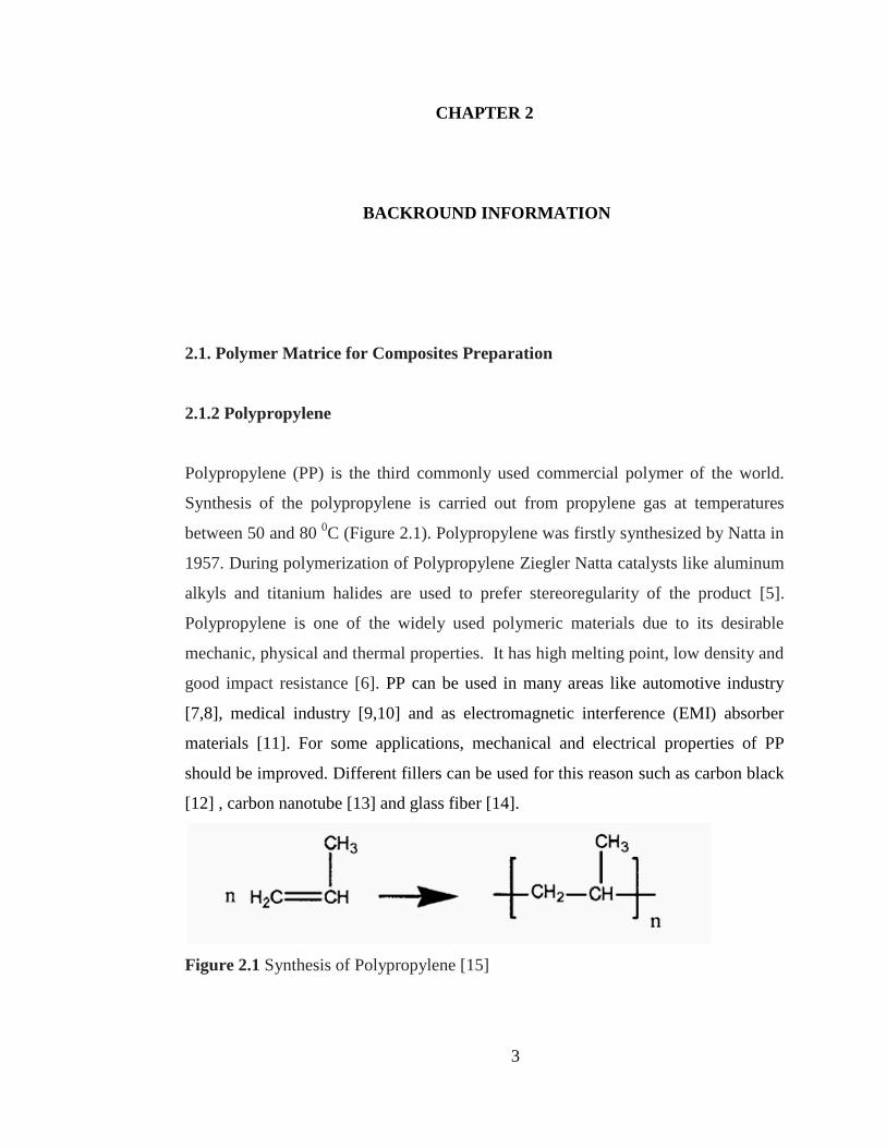
Polypropylene (PP) is the third commonly used commercial polymer of the world.
Synthesis of the polypropylene is carried out from propylene gas at temperatures
between 50 and 80 0C (Figure 2.1). Polypropylene was firstly synthesized by Natta in
1957. During polymerization of Polypropylene Ziegler Natta catalysts like aluminum
alkyls and titanium halides are used to prefer stereoregularity of the product [5].
Polypropylene is one of the widely used polymeric materials due to its desirable
mechanic, physical and thermal properties. It has high melting point, low density and
good impact resistance [6]. PP can be used in many areas like automotive industry
[7,8], medical industry [9,10] and as electromagnetic interference (EMI) absorber
materials [11]. For some applications, mechanical and electrical properties of PP
should be improved. Different fillers can be used for this reason such as carbon black
[12] , carbon nanotube [13] and glass fiber [14].
Figure 2.1 Synthesis of Polypropylene [15]
4
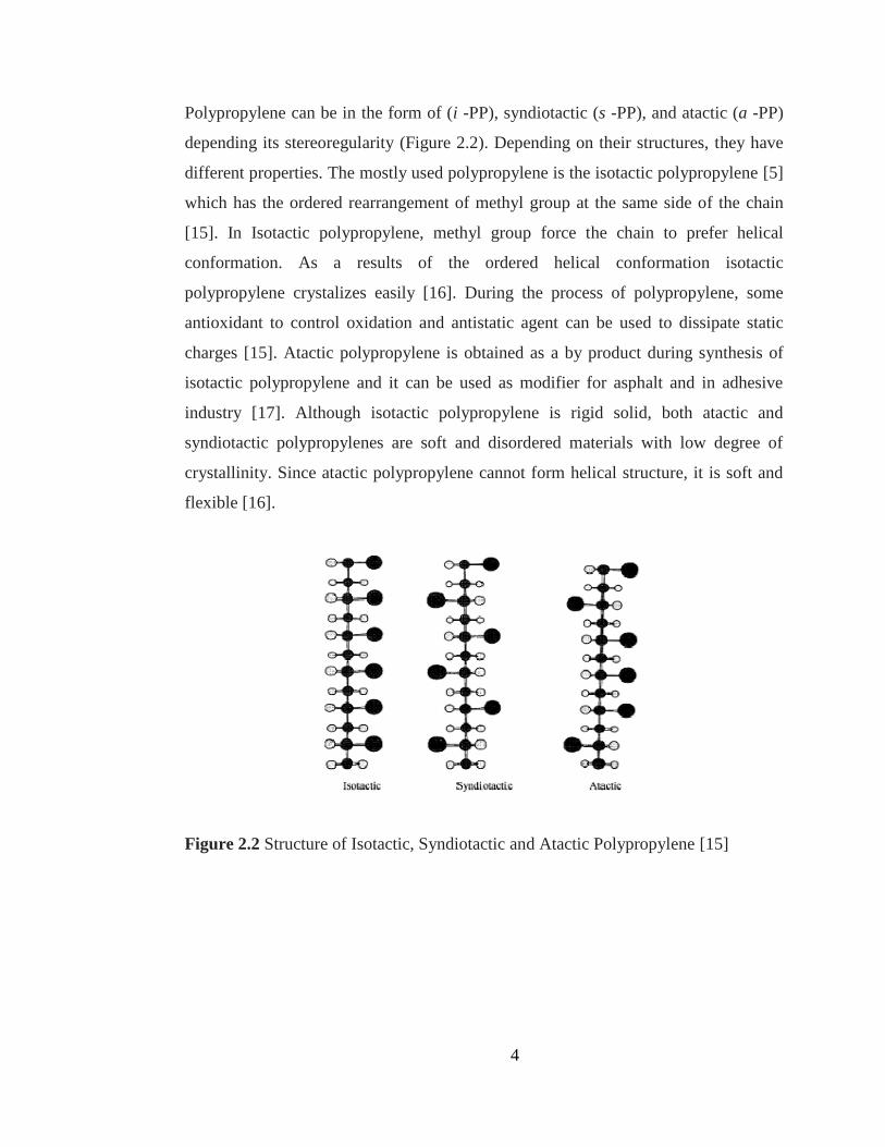
Polypropylene can be in the form of (i -PP), syndiotactic (s -PP), and atactic (a -PP)
depending its stereoregularity (Figure 2.2). Depending on their structures, they have
different properties. The mostly used polypropylene is the isotactic polypropylene [5]
which has the ordered rearrangement of methyl group at the same side of the chain
[15]. In Isotactic polypropylene, methyl group force the chain to prefer helical
conformation. As a results of the ordered helical conformation isotactic
polypropylene crystalizes easily [16]. During the process of polypropylene, some
antioxidant to control oxidation and antistatic agent can be used to dissipate static
charges [15]. Atactic polypropylene is obtained as a by product during synthesis of
isotactic polypropylene and it can be used as modifier for asphalt and in adhesive
industry [17]. Although isotactic polypropylene is rigid solid, both atactic and
syndiotactic polypropylenes are soft and disordered materials with low degree of
crystallinity. Since atactic polypropylene cannot form helical structure, it is soft and
flexible [16].
Figure 2.2 Structure of Isotactic, Syndiotactic and Atactic Polypropylene [15]
5
2.2. Polymer Dielectric for Organic Field Effect Transistor
2.2.1. Polyethylene
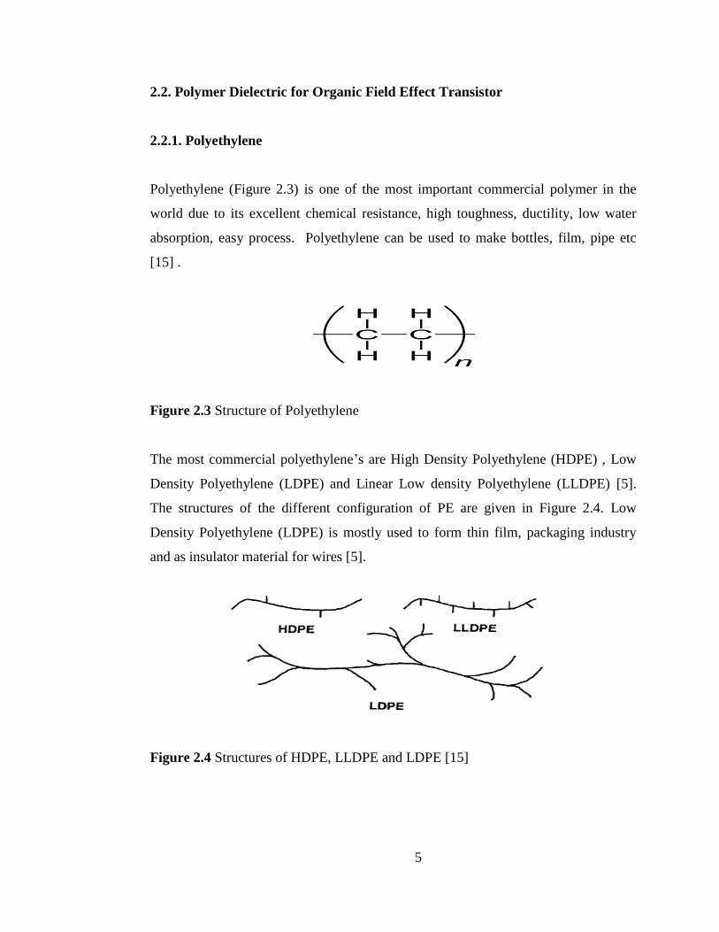
Polyethylene (Figure 2.3) is one of the most important commercial polymer in the
world due to its excellent chemical resistance, high toughness, ductility, low water
absorption, easy process. Polyethylene can be used to make bottles, film, pipe etc
[15] .
Figure 2.3 Structure of Polyethylene
The most commercial polyethylene‟s are High Density Polyethylene (HDPE) , Low
Density Polyethylene (LDPE) and Linear Low density Polyethylene (LLDPE) [5].
The structures of the different configuration of PE are given in Figure 2.4. Low
Density Polyethylene (LDPE) is mostly used to form thin film, packaging industry
and as insulator material for wires [5].
Figure 2.4 Structures of HDPE, LLDPE and LDPE [15]
6
LDPE is the first synthesized polyethylene in 1939. LDPE has partially crystalline
structure and its crystallinity differs between 50 % and 70 %. The melting
temperature of LDPE is about between 100 and 120 0C. LDPE has branched structure
and size of the side chains determine the crystallinity of the LDPE. LLDPE has
shorter branching than the LDPE. Branches are limited in HDPE in contrast to
LLDPE and LDPE. Physical properties of LDPE depend on the degree of crystallinity
and molecular weight. The properties of the PE such as tensile strength, opacity,
rigidity, chemical strength depend on degree of crystallinity. These properties are
increased with decreasing short chain branching. If the crystallinity decreases,
permeability to liquid or gases and toughness of the material increase [5].
Highly stable and trap-free dielectrics are crucial in the fabrication of high-
performance organic field effect transistors (OFET‟s) [18,19]. Owing to its excellent
insulating properties (band gap of ~8.8 eV)[20], and extremely low conductivity
(~9×10-17
-1
cm-1
)[21] , low toxicity, chemical inertness and stability [15],
polyethylene represents an interesting choice for the dielectric layer in organic
devices.
2.3. Conductive Fillers
2.3.1. Carbon Nanotubes
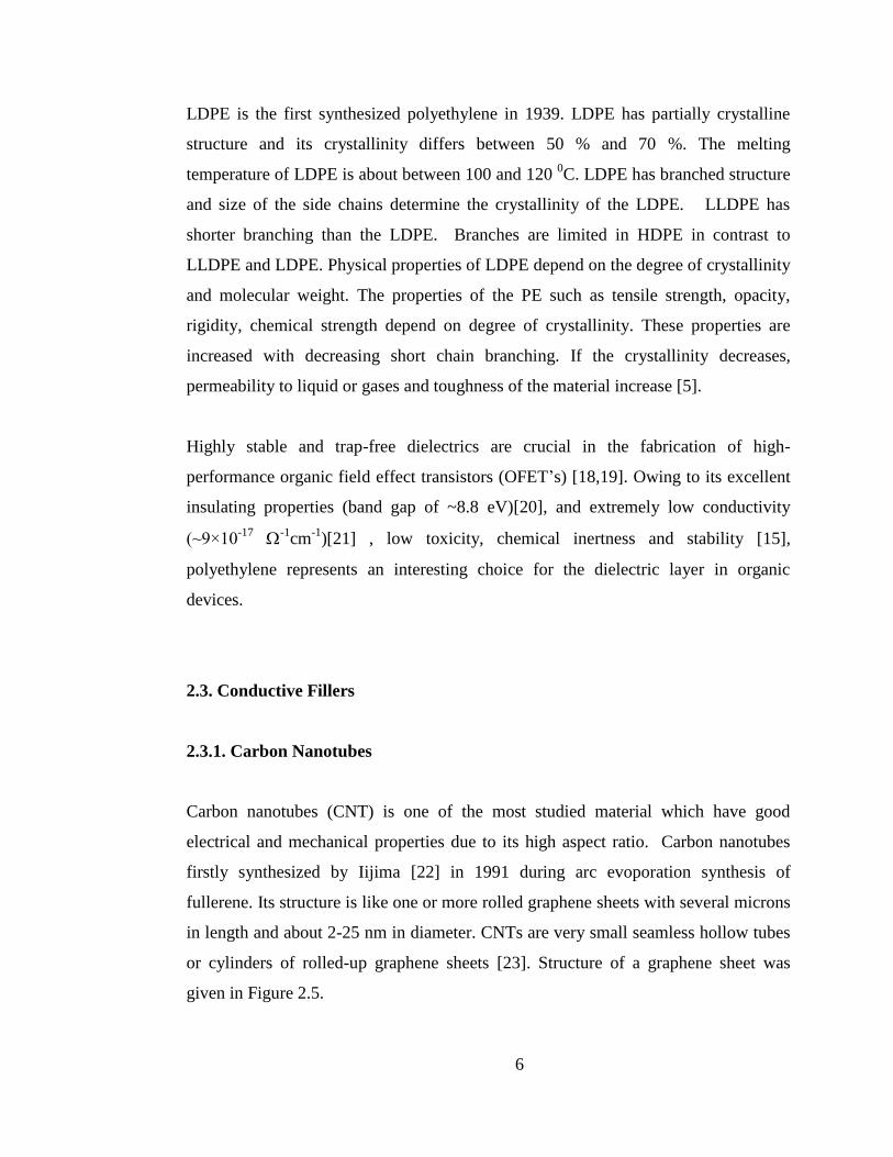
Carbon nanotubes (CNT) is one of the most studied material which have good
electrical and mechanical properties due to its high aspect ratio. Carbon nanotubes
firstly synthesized by Iijima [22] in 1991 during arc evoporation synthesis of
fullerene. Its structure is like one or more rolled graphene sheets with several microns
in length and about 2-25 nm in diameter. CNTs are very small seamless hollow tubes
or cylinders of rolled-up graphene sheets [23]. Structure of a graphene sheet was
given in Figure 2.5.
7
Figure 2.5 Structure of graphene sheet [23]
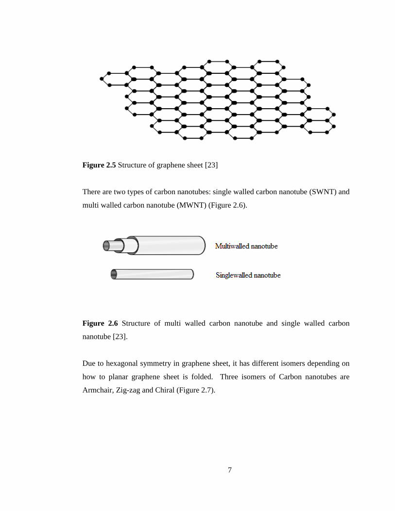
There are two types of carbon nanotubes: single walled carbon nanotube (SWNT) and
multi walled carbon nanotube (MWNT) (Figure 2.6).
Figure 2.6 Structure of multi walled carbon nanotube and single walled carbon
nanotube [23].
Due to hexagonal symmetry in graphene sheet, it has different isomers depending on
how to planar graphene sheet is folded. Three isomers of Carbon nanotubes are
Armchair, Zig-zag and Chiral (Figure 2.7).
8
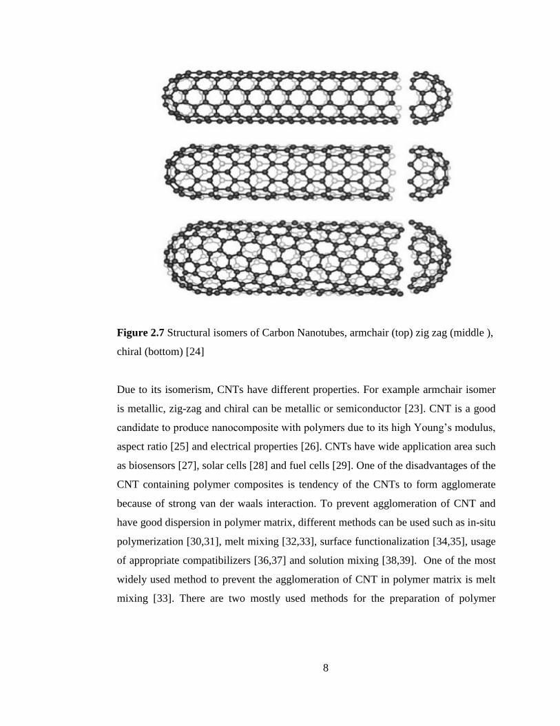
Figure 2.7 Structural isomers of Carbon Nanotubes, armchair (top) zig zag (middle ),
chiral (bottom) [24]
Due to its isomerism, CNTs have different properties. For example armchair isomer
is metallic, zig-zag and chiral can be metallic or semiconductor [23]. CNT is a good
candidate to produce nanocomposite with polymers due to its high Young‟s modulus,
aspect ratio [25] and electrical properties [26]. CNTs have wide application area such
as biosensors [27], solar cells [28] and fuel cells [29]. One of the disadvantages of the
CNT containing polymer composites is tendency of the CNTs to form agglomerate
because of strong van der waals interaction. To prevent agglomeration of CNT and
have good dispersion in polymer matrix, different methods can be used such as in-situ
polymerization [30,31], melt mixing [32,33], surface functionalization [34,35], usage
of appropriate compatibilizers [36,37] and solution mixing [38,39]. One of the most
widely used method to prevent the agglomeration of CNT in polymer matrix is melt
mixing [33]. There are two mostly used methods for the preparation of polymer
9
/carbon nanotube nanocomposites. These methods are solution mixing and melt
mixing.
Bikiaris et al. [40] prepared polypropylene nanocomposites with surface modified
CNTs. which were functionalized with HNO3/H2SO4 (1:3 in volume ratio).
Polypropylene/CNT composites were prepared with CNTs which prepared with
different treatment time with acid. During acid treatment, length of the carbon
nanotubes decreased and composites which prepared with surface treated CNT
showed higher mechanical properties than the neat CNT /PP composites. Length
reduction of CNT decreased the agglomeration ability of the CNTs. Zhou et al. [34]
functionalized CNT with silane coupling agent and then grafted 3-
methacryloxypropyltrimetoxysilane on CNT. After surface modification, CNT
showed good interfacial adhesion with polypropylene and dispersion of the CNT was
better than neat CNT.
Kashiwagi et al.[41] studied the thermal and flammability properties of the PP/CNT
composites prepared by melt mixing. Addition of the CNT to polymer matrix
increased thermal stability of the polymer matrix. Lee et al. [36] studied the effect of
compatibilizer on rheological and electrical properties of acid, amine and heat treated
CNT. Composites prepared with amine and acid treated CNT showed higher
electrical properties than untreated CNT.
Logakis et al. [42] blended PP and CNT at 180 0C (speed was 200 rpm) for 30
minutes under N2 atmosphere. They found the percolation threshold as 0.6 vol %.
Prashanta et al. [43] prepared masterbach based composites of PP/CNT. They figured
out that addition of CNT, impact resistance of notched samples increased but in
contrast with this for unnotched samples impact resistance decreased. CNT addition
made crack initiation easier but crack propagation was limited.
10
Beside melt mixing or solution mixing different techniques can be applied to carbon
nanotubes like surface functionalization or usage of appropriate compatibilizers to
improve their dispersion in polymer matrix. Surface functionalization with proper
functional groups improves the dispersability of carbon nanotubes in polymer matrix
or solvent and enhance the ability of the carbon nanotubes to do strong interfacial
interaction with polymer [44].
2.3.2. Carbon Black
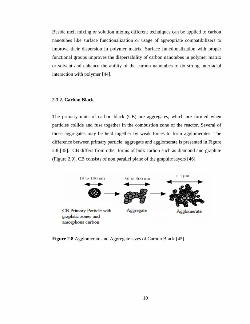
The primary units of carbon black (CB) are aggregates, which are formed when
particles collide and fuse together in the combustion zone of the reactor. Several of
those aggregates may be held together by weak forces to form agglomerates. The
difference between primary particle, aggregate and agglomerate is presented in Figure
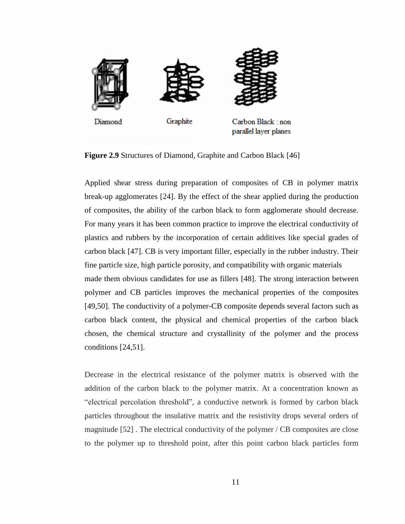
2.8 [45]. CB differs from other forms of bulk carbon such as diamond and graphite
(Figure 2.9). CB consists of non parallel plane of the graphite layers [46].
Figure 2.8 Agglomerate and Aggregate sizes of Carbon Black [45]
11
Figure 2.9 Structures of Diamond, Graphite and Carbon Black [46]
Applied shear stress during preparation of composites of CB in polymer matrix
break-up agglomerates [24]. By the effect of the shear applied during the production
of composites, the ability of the carbon black to form agglomerate should decrease.
For many years it has been common practice to improve the electrical conductivity of
plastics and rubbers by the incorporation of certain additives like special grades of
carbon black [47]. CB is very important filler, especially in the rubber industry. Their
fine particle size, high particle porosity, and compatibility with organic materials
made them obvious candidates for use as fillers [48]. The strong interaction between
polymer and CB particles improves the mechanical properties of the composites
[49,50]. The conductivity of a polymer-CB composite depends several factors such as
carbon black content, the physical and chemical properties of the carbon black
chosen, the chemical structure and crystallinity of the polymer and the process
conditions [24,51].
Decrease in the electrical resistance of the polymer matrix is observed with the
addition of the carbon black to the polymer matrix. At a concentration known as
“electrical percolation threshold”, a conductive network is formed by carbon black
particles throughout the insulative matrix and the resistivity drops several orders of
magnitude [52] . The electrical conductivity of the polymer / CB composites are close
to the polymer up to threshold point, after this point carbon black particles form
12
conductive network in polymer matrix [53,54] and conductivity of the polymer
matrix increases several order magnitude [24]. This threshold occurs in the range
from 3 to 15 wt % for CB [24].
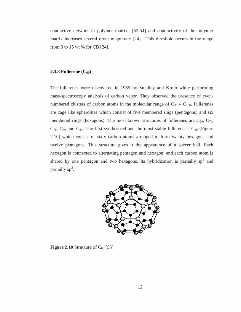
2.3.3 Fullerene (C60)
The fullerenes were discovered in 1985 by Smaliey and Kroto while performing
mass-spectroscopy analysis of carbon vapor. They observed the presence of even-
numbered clusters of carbon atoms in the molecular range of C30 – C100. Fullerenes
are cage like spherolites which consist of five membered rings (pentagons) and six
membered rings (hexagons). The most known structures of fullerenes are C60, C70,
C78, C76 and C84. The first synthesized and the most stable fullerene is C60 (Figure
2.10) which consist of sixty carbon atoms arranged to form twenty hexagons and
twelve pentagons. This structure gives it the appearance of a soccer ball. Each
hexagon is connected to alternating pentagon and hexagon, and each carbon atom is
shared by one pentagon and two hexagons. Its hybridization is partially sp3 and
partially sp2.
Figure 2.10 Structure of C60 [55]
13
C60 aggregates can be considered as softest of the solid phases of carbon. However,
they can be compressed to the 70 % of its original volume [55]. The colors of the
fullerene family vary according to their molecular weight and symmetry. Their colors
in solution with respect to fullerene type are magenta (C60), port-wine red (C70),
brown (C76 and C78), and yellow-green (C84). C60 is insoluble or sparingly soluble in
most solvents and that is why it is hard to handle [56]. Because of this problem
different groups studied to obtain soluble fullerene derivatives.
Fullerenes and fullerene derivatives have been shown to possess interesting photonic,
electronic, superconducting, magnetic, lubrication and biomedical properties due to
their structure [57]. Low solubility and poor miscibility of fullerenes limit its
application and its ability to form self aggregate cause phase separation problems
[58,59].
Surface functionalization of the fullerenes and carbon nanotubes to improve their
compatibility has become important subject in recent years [60]. Since fullerenes and
carbon nanotubes have no hyrogen atoms or other groups on their surface, they
cannot undergo substitution reaction. For this reason they need surface modification
in order to do further functionalization on their surface [58].
2.4. Composites and Nanocomposites
Composites are made with the combination of two materials to give the unique
properties of materials in one material [61]. The properties of the composites depend
on the type of the filler, matrix and interface between filler and polymer chains.
Interface between polymer and filler is important to provide better load transfer. Size,
shape, orientation and dispersion of the filler are other factors affecting the properties
of the composites [62].
14
The reinforcement length scale is in micrometers, and the interface of fillers is close
to the bulk polymer matrix. In the case of nanocomposites, where the length scale of
the reinforcement (nanoparticles) is in nanometer scale, they have ultralarge
interfacial area per volume, and the distances between the polymer and filler
components are extremely short. Polymer coils are 40 nm in diameter, and the
nanoparticles are on the same order of magnitude as the polymer [63].
Apart from the properties of individual components in a nanocomposite, interfaces
play an important role in enhancing or limiting the overall properties of the system.
Due to the high surface area of nanostructures, nanocomposites present many
interfaces between the constituent intermixed phases. Special properties of
nanocomposite materials often arise from interaction of its phases at the interfaces.
An excellent example of this phenomenon is the mechanical behavior of nanotube-
filled polymer composites. Although addition nanotubes could conceivably improve
the strength of polymers (due to the superior mechanical properties of the nanotubes),
poor interaction serves only to create weak regions in the composite, resulting in no
enhancement of its mechanical properties [64].
2.5. Conductive Polymer Composites
Polymeric materials can be intrinsically conductive due to their conjugated bonds or
doping with an appropriate material. If the polymer is not conductive (polymers
which have no conjugated structure), conductive polymer composites can be prepared
with addition of a conductive filler such as metal powder, carbon black and graphite.
Structures of some conjugated polymers are given in Figure 2.11. By addition of
conductive filler, conductivity of the polymeric material increases by several orders
of magnitude. This conductivity increase depends on the concentration and the
character of the filling material. Conductivity of the material depends on the
interaction of filling material and polymer chains. By mixing the filler with polymer,
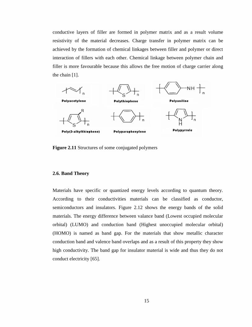
15
conductive layers of filler are formed in polymer matrix and as a result volume
resistivity of the material decreases. Charge transfer in polymer matrix can be
achieved by the formation of chemical linkages between filler and polymer or direct
interaction of fillers with each other. Chemical linkage between polymer chain and
filler is more favourable because this allows the free motion of charge carrier along
the chain [1].
Figure 2.11 Structures of some conjugated polymers
2.6. Band Theory
Materials have specific or quantized energy levels according to quantum theory.
According to their conductivities materials can be classified as conductor,
semiconductors and insulators. Figure 2.12 shows the energy bands of the solid
materials. The energy difference between valance band (Lowest occupied molecular
orbital) (LUMO) and conduction band (Highest unoccupied molecular orbital)
(HOMO) is named as band gap. For the materials that show metallic character
conduction band and valence band overlaps and as a result of this property they show
high conductivity. The band gap for insulator material is wide and thus they do not
conduct electricity [65].
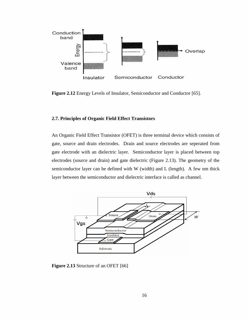
16
Figure 2.12 Energy Levels of Insulator, Semiconductor and Conductor [65].
2.7. Principles of Organic Field Effect Transistors
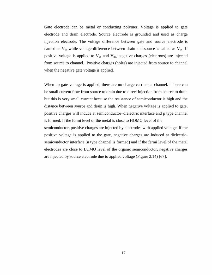
An Organic Field Effect Transistor (OFET) is three terminal device which consists of
gate, source and drain electrodes. Drain and source electrodes are seperated from
gate electrode with an dielectric layer. Semiconductor layer is placed between top
electrodes (source and drain) and gate dielectric (Figure 2.13). The geometry of the
semiconductor layer can be defined with W (width) and L (length). A few nm thick
layer between the semiconductor and dielectric interface is called as channel.
Figure 2.13 Structure of an OFET [66]
17
Gate electrode can be metal or conducting polymer. Voltage is applied to gate
electrode and drain electrode. Source electrode is grounded and used as charge
injection electrode. The voltage difference between gate and source electrode is
named as Vgs while voltage difference between drain and source is called as Vds. If
positive voltage is applied to Vgs and Vds, negative charges (electrons) are injected
from source to channel. Positive charges (holes) are injected from source to channel
when the negative gate voltage is applied.
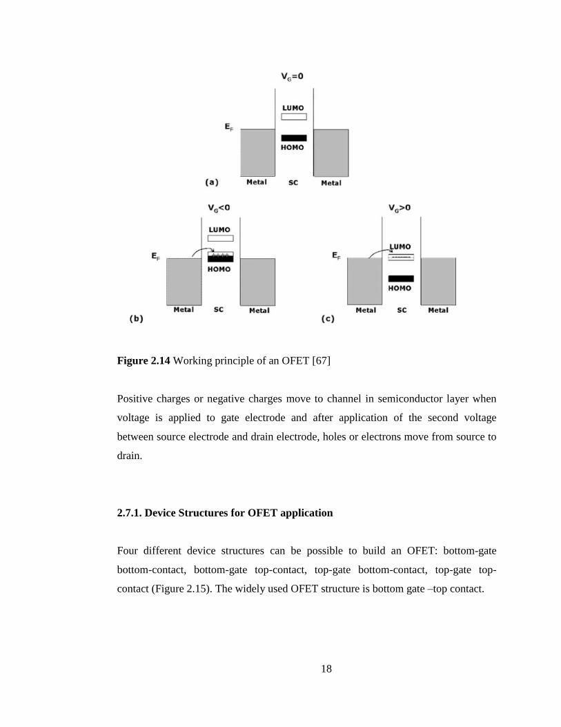
When no gate voltage is applied, there are no charge carriers at channel. There can
be small current flow from source to drain due to direct injection from source to drain
but this is very small current because the resistance of semiconductor is high and the
distance between source and drain is high. When negative voltage is applied to gate,
positive charges will induce at semiconductor–dielectric interface and p type channel
is formed. If the fermi level of the metal is close to HOMO level of the
semiconductor, positive charges are injected by electrodes with applied voltage. If the
positive voltage is applied to the gate, negative charges are induced at dielectric-
semiconductor interface (n type channel is formed) and if the fermi level of the metal
electrodes are close to LUMO level of the organic semiconductor, negative charges
are injected by source electrode due to applied voltage (Figure 2.14) [67].
18
Figure 2.14 Working principle of an OFET [67]
Positive charges or negative charges move to channel in semiconductor layer when
voltage is applied to gate electrode and after application of the second voltage
between source electrode and drain electrode, holes or electrons move from source to
drain.
2.7.1. Device Structures for OFET application
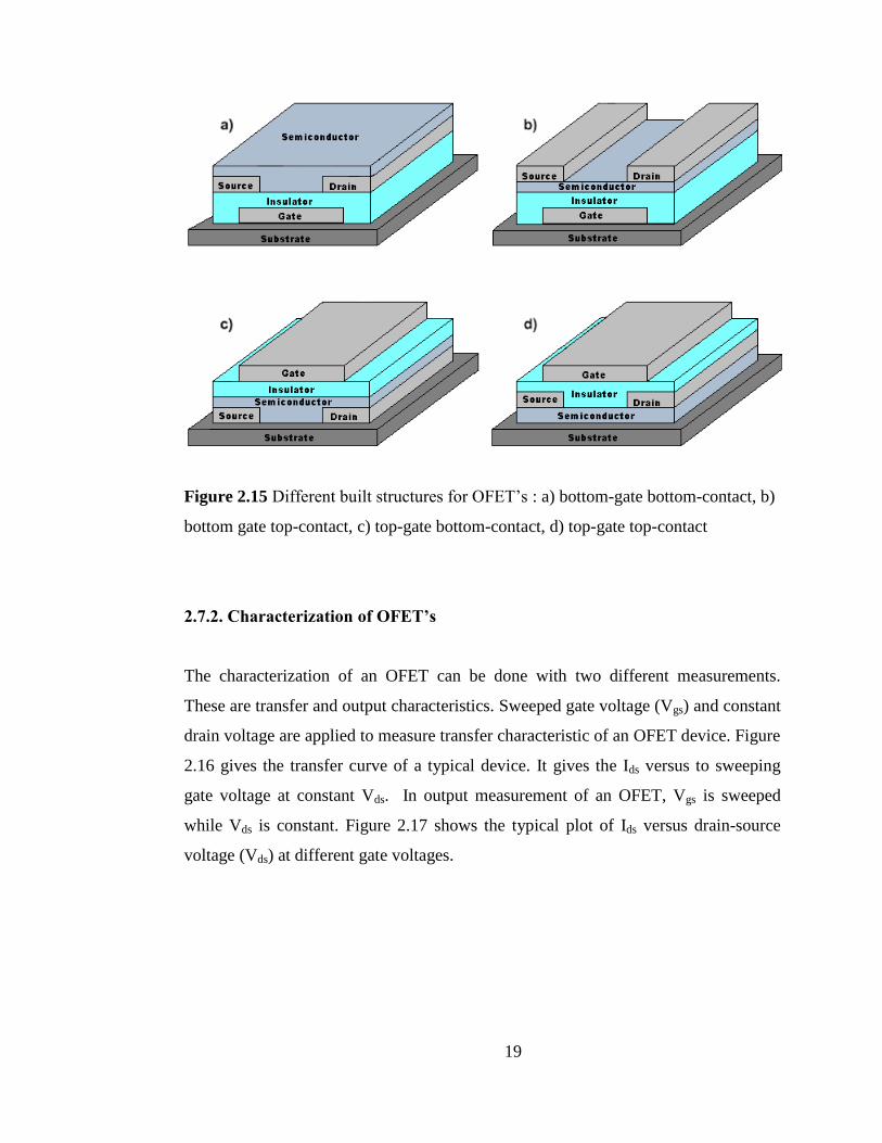
Four different device structures can be possible to build an OFET: bottom-gate
bottom-contact, bottom-gate top-contact, top-gate bottom-contact, top-gate top-
contact (Figure 2.15). The widely used OFET structure is bottom gate –top contact.
19
Figure 2.15 Different built structures for OFET‟s : a) bottom-gate bottom-contact, b)
bottom gate top-contact, c) top-gate bottom-contact, d) top-gate top-contact
2.7.2. Characterization of OFET’s
The characterization of an OFET can be done with two different measurements.
These are transfer and output characteristics. Sweeped gate voltage (Vgs) and constant
drain voltage are applied to measure transfer characteristic of an OFET device. Figure
2.16 gives the transfer curve of a typical device. It gives the Ids versus to sweeping
gate voltage at constant Vds. In output measurement of an OFET, Vgs is sweeped
while Vds is constant. Figure 2.17 shows the typical plot of Ids versus drain-source
voltage (Vds) at different gate voltages.
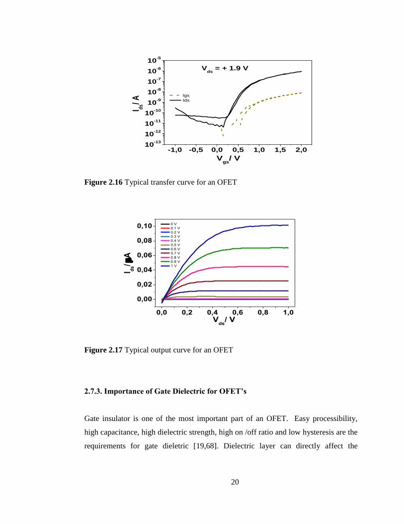
20
-1,0 -0,5 0,0 0,5 1,0 1,5 2,010
-13
10-12
10-11
10-10
10-9
10-8
10-7
10-6
10-5
I ds/ A
Vgs
/ V
Igs
Ids
Vds
= + 1.9 V
Figure 2.16 Typical transfer curve for an OFET
0,0 0,2 0,4 0,6 0,8 1,0
0,00
0,02
0,04
0,06
0,08
0,10
I ds/ A
Vds
/ V
0 V
0.1 V
0.2 V
0.3 V
0.4 V
0.5 V
0.6 V
0.7 V
0.8 V
0.9 V
1 V
Figure 2.17 Typical output curve for an OFET
2.7.3. Importance of Gate Dielectric for OFET’s
Gate insulator is one of the most important part of an OFET. Easy processibility,
high capacitance, high dielectric strength, high on /off ratio and low hysteresis are the
requirements for gate dieletric [19,68]. Dielectric layer can directly affect the
21
performance of an OFET device. The interaction between dielectric and organic
semiconductor affects the morphology of the organic semiconductor. Beside this
surface roughness of the dielectric layer is another important factor for OFET. If the
dielectric layer is rough and it contains valleys at interface, these parts behave as
charge trap. Field effect mobility is increased with increasing grain size of the organic
semiconductor. High gate capacitance is another important property for gate
dielectrics. Since high capacitance of the dielectric layer allows the high charge
density induce at low voltages. Capacitance of the transistors can be increased by
decreasing the thickness of the dielectric layer or with usage of high dielectric
constant material [19].
When electric field is applied to dielectric material, material changes its charge
distribution. As a result of this field induced polarization, material works as capacitor.
Material should have large band gap to be an insulator. If there is an excitation state
available material will not work as insulator. But if the applied voltage is higher than
breakdown voltage material loses its insulating property [68]. Capacitance of the
material between two metal layer is directly proportional with the dielectric constant
of the material with the formula of C = ε(k/d) where C is the capacitance, ε is the
vacuum permittivity constant, k is the dielectric constant, d is the thickness of the
dielectric layer. Capacitance of the dielectric layer increases with decreasing layer
thickness [68].
Decreasing the operation voltage is critically important for some applications of
OFETs. Three main factors affecting the operation voltage are: mobility of the
semiconductor, capacitance of the dielectric and geometry of the channel. Relation of
these factors with operation voltage is given with this formula:
22
where W is the channel width, L is channel length, C0 is capacitance per unit area,
VG is gate voltage, VT is threshold voltage, VD is drain voltage, µ is the mobility.
Geometry of the channel can be changed to decrease the operation voltage, but the
application of this method is limited due to limitations of the shadow mask and
printing techniques. Mobility of the semiconductor can not be altered because its
intrinsic property of the semiconductor material. The only reasonable way to decrease
the operation voltage is increasing the capacitance of the dielectric layer by
decreasing thickness of the insulator layer or usage of high dielectric constant
material.
2.7.4. Technigues for OFET Preparation
Different techniques can be used during the preparation of device. Spin coating and
vacuum evaporation are the most commonly used techniques for the preparation of
dielectric and semiconductor layer of an OFET.
Vacuum evaporation of melamin were done by Vladu et al. [69]. They prepared
transistor with vacuum processed melamin layer and C60 as semiconductor layer.
They build transistors working at 15V with 4 orders of magnitude on/off ratio. The
advantage of the vacuum evaporation is that it is free from the impurities coming
from solvent, which can cause hysteresis. Impurities coming from the dielectric layer
can cause hysteresis, too. Egginger et al. [70] worked on the effect of the impurities
coming from PVA dielectric on hysteresis. Vladu et al. prepared OFET which consist
totaly biodegredable materials [71] . Both spin coating and vacuum evaporation
techniques were used in this study. Vacuum evaporation is not useful only for small
molecules. It can be also used for the evaporation of the polymers, too. Vacuum
evaporation of polyaniline was done by Vladu and coworkers [72]. They prepared
devices which contain polyaniline gate dielectric and C60 semiconductor layer by

23
using vacuum evaporation technique. Root mean square roughness (RMS) of 1.75 µm
polyaniline film prepared by vacuum evaporation technique was 10 nm.
In this study, chemical vacuum deposition technique was used for evaporation of low
density polyethylene gate dielectric, fullerene and pentace layers.
24
CHAPTER 3
EXPERIMENTAL
In this dissertation, Polypropylene/Carbon Black, Polypropylene/Carbon Nanotube,
Polypropylene/Fullerene composites and transistors which are built with the
polyethylene gate dielectric were studied. Before preperation of
Polypropylene/Carbon Nanotube, Polypropylene/Fullerene composites, carbon
nanotube and fullerene were fuctionalized with H2SO4/HNO3. Details of composite
preparation ,surface functionalization and transistor preperation were given in
experimental part.
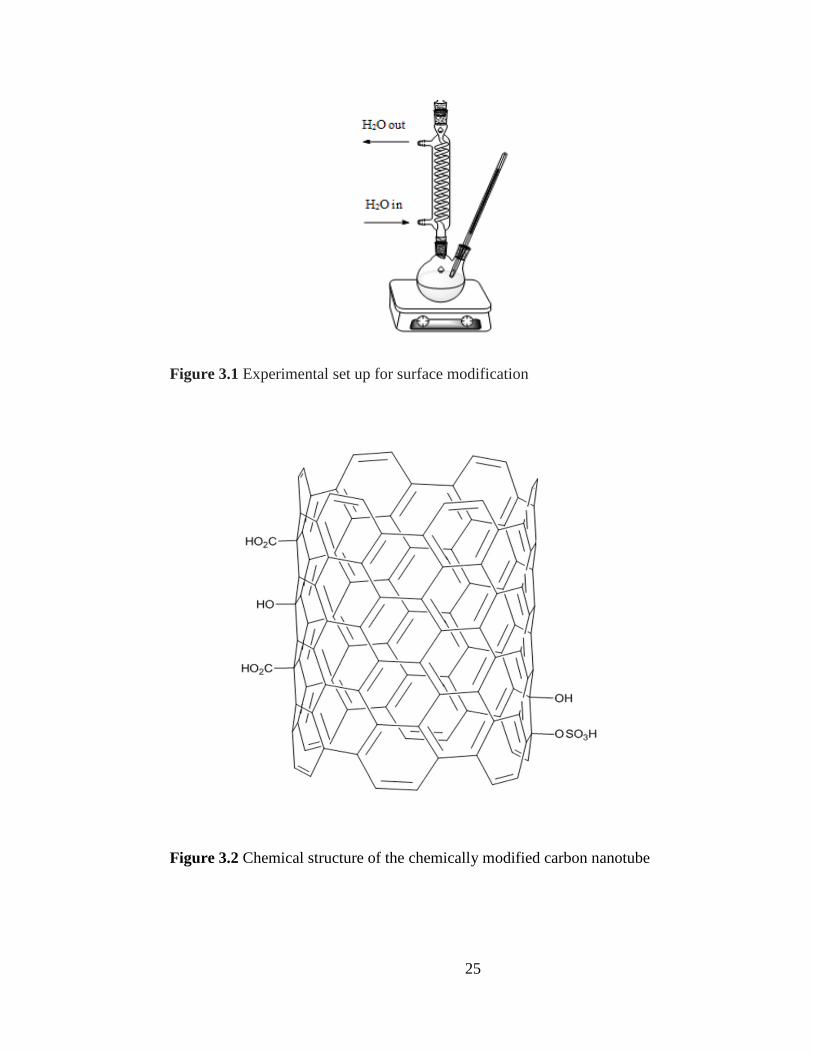
3.1. Surface Modification of Carbon nanotube with HNO3/H2SO4
Multi walled carbon nanotube (Nanocyl 7000) purchased from Nanocyl was used in
this study. Concentrated H2SO4 (95-98 %) and HNO3 (65 %) were supplied from
Merck. Carbon Nanotubes were refluxed with concentrated H2SO4-HNO3 mixture at
different ratios (1:1, 1:1.6, (v/v), HNO3 : H2SO4) at 900C for 5 h to form a brown
suspension (Figure 3.1). The materials were named as CN 1 and CN 2 respectively.
Then the suspension was diluted with distilled water (200 mL) and stirred for 2 hours.
After this process reaction mixture was filtrated and washed with distilled water.
Then the obtained black solid is dried in vacuum owen [73]. The chemical structure
of the chemically modified Carbon Nanotube with H2SO4/HNO3 is given in Figure
3.2.
25
Figure 3.1 Experimental set up for surface modification
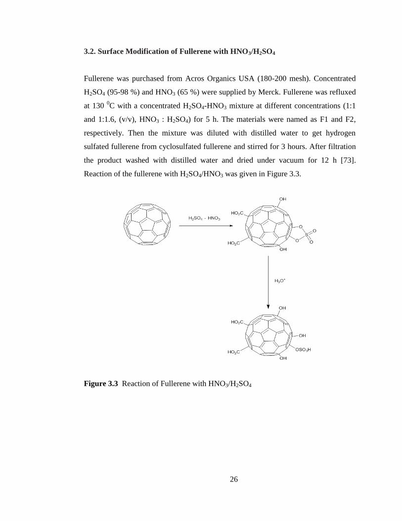
Figure 3.2 Chemical structure of the chemically modified carbon nanotube
26
3.2. Surface Modification of Fullerene with HNO3/H2SO4
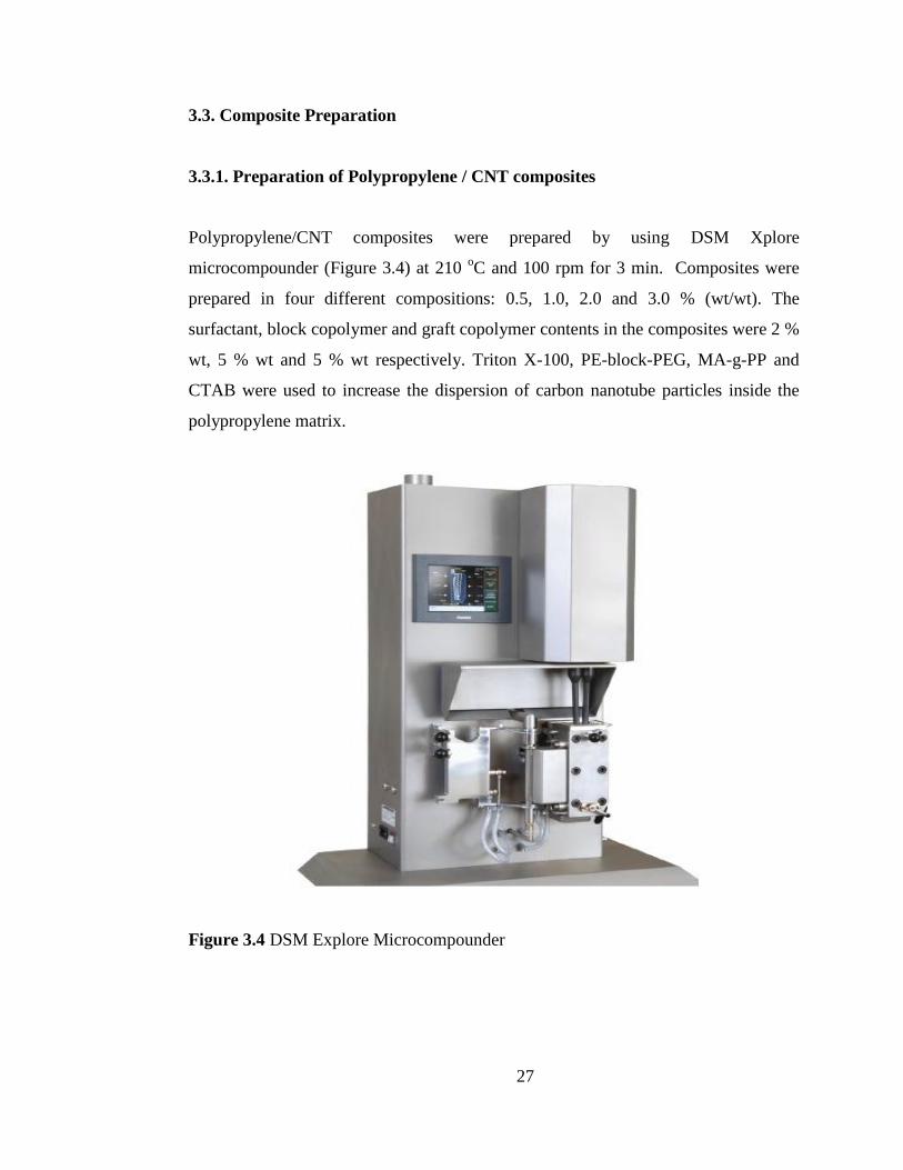
Fullerene was purchased from Acros Organics USA (180-200 mesh). Concentrated
H2SO4 (95-98 %) and HNO3 (65 %) were supplied by Merck. Fullerene was refluxed
at 130 0C with a concentrated H2SO4-HNO3 mixture at different concentrations (1:1
and 1:1.6, (v/v), HNO3 : H2SO4) for 5 h. The materials were named as F1 and F2,
respectively. Then the mixture was diluted with distilled water to get hydrogen
sulfated fullerene from cyclosulfated fullerene and stirred for 3 hours. After filtration
the product washed with distilled water and dried under vacuum for 12 h [73].
Reaction of the fullerene with H2SO4/HNO3 was given in Figure 3.3.
Figure 3.3 Reaction of Fullerene with HNO3/H2SO4
27
3.3. Composite Preparation
3.3.1. Preparation of Polypropylene / CNT composites
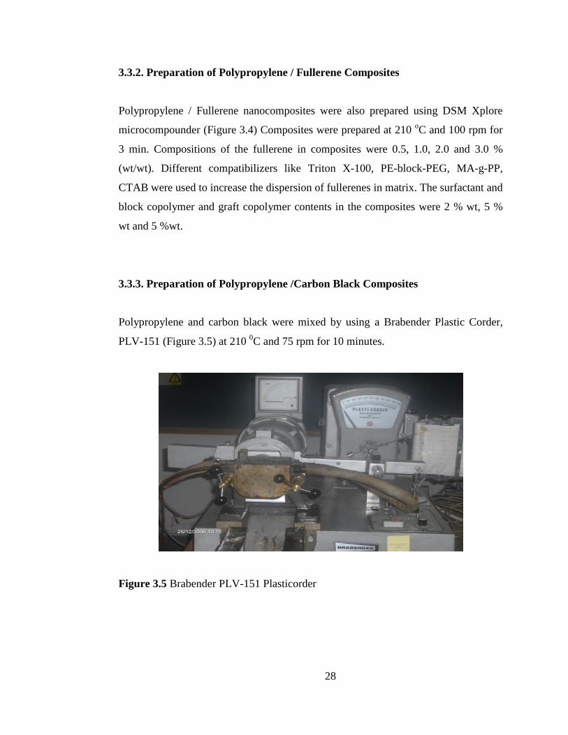
Polypropylene/CNT composites were prepared by using DSM Xplore
microcompounder (Figure 3.4) at 210 oC and 100 rpm for 3 min. Composites were
prepared in four different compositions: 0.5, 1.0, 2.0 and 3.0 % (wt/wt). The
surfactant, block copolymer and graft copolymer contents in the composites were 2 %
wt, 5 % wt and 5 % wt respectively. Triton X-100, PE-block-PEG, MA-g-PP and
CTAB were used to increase the dispersion of carbon nanotube particles inside the
polypropylene matrix.
Figure 3.4 DSM Explore Microcompounder
28
3.3.2. Preparation of Polypropylene / Fullerene Composites
Polypropylene / Fullerene nanocomposites were also prepared using DSM Xplore
microcompounder (Figure 3.4) Composites were prepared at 210 oC and 100 rpm for
3 min. Compositions of the fullerene in composites were 0.5, 1.0, 2.0 and 3.0 %
(wt/wt). Different compatibilizers like Triton X-100, PE-block-PEG, MA-g-PP,
CTAB were used to increase the dispersion of fullerenes in matrix. The surfactant and
block copolymer and graft copolymer contents in the composites were 2 % wt, 5 %
wt and 5 %wt.
3.3.3. Preparation of Polypropylene /Carbon Black Composites
Polypropylene and carbon black were mixed by using a Brabender Plastic Corder,
PLV-151 (Figure 3.5) at 210 0C and 75 rpm for 10 minutes.
Figure 3.5 Brabender PLV-151 Plasticorder
29
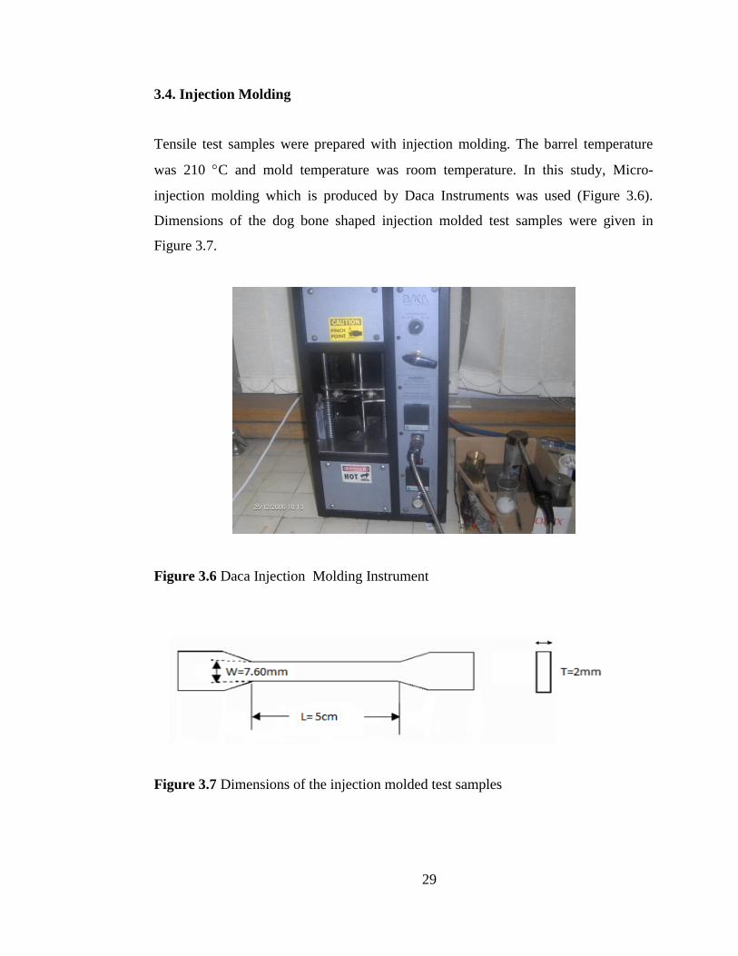
3.4. Injection Molding
Tensile test samples were prepared with injection molding. The barrel temperature
was 210 C and mold temperature was room temperature. In this study, Micro-
injection molding which is produced by Daca Instruments was used (Figure 3.6).
Dimensions of the dog bone shaped injection molded test samples were given in
Figure 3.7.
Figure 3.6 Daca Injection Molding Instrument
Figure 3.7 Dimensions of the injection molded test samples
30
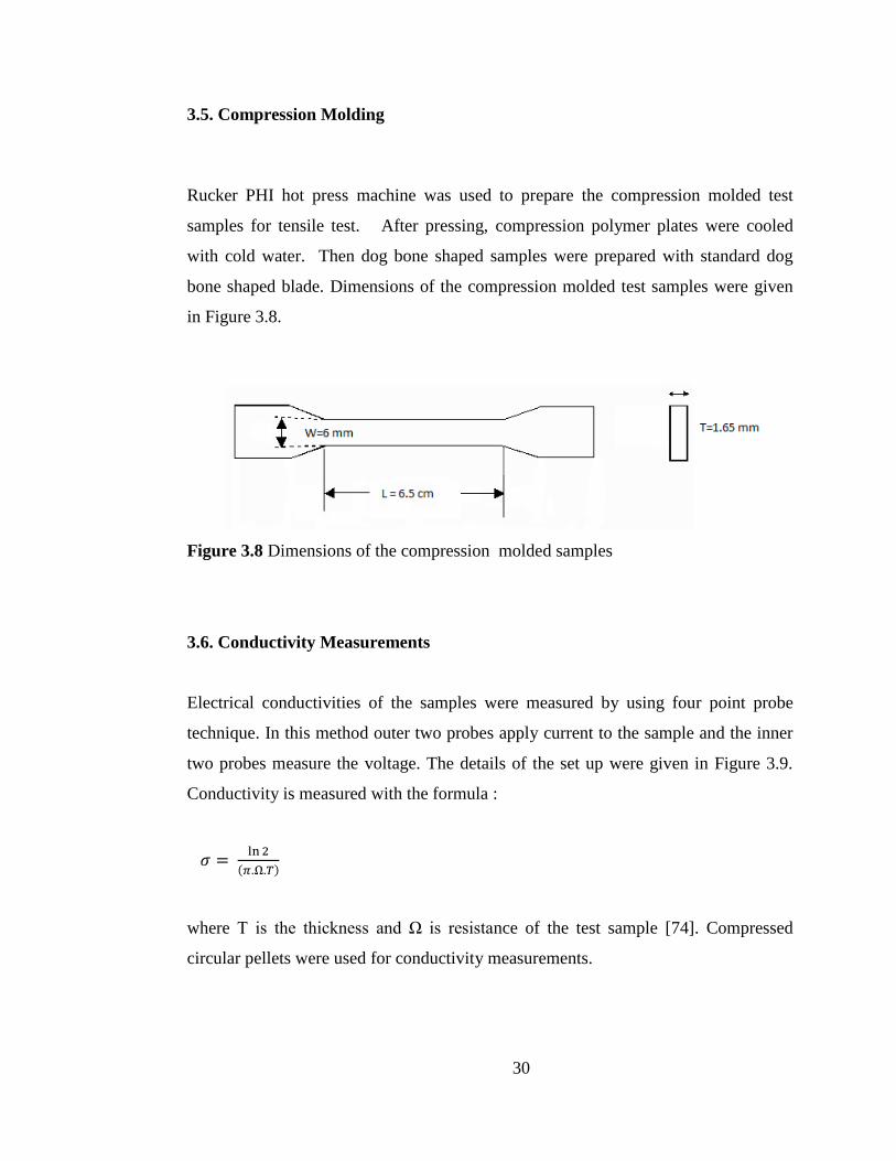
3.5. Compression Molding
Rucker PHI hot press machine was used to prepare the compression molded test
samples for tensile test. After pressing, compression polymer plates were cooled
with cold water. Then dog bone shaped samples were prepared with standard dog
bone shaped blade. Dimensions of the compression molded test samples were given
in Figure 3.8.
Figure 3.8 Dimensions of the compression molded samples
3.6. Conductivity Measurements
Electrical conductivities of the samples were measured by using four point probe
technique. In this method outer two probes apply current to the sample and the inner
two probes measure the voltage. The details of the set up were given in Figure 3.9.
Conductivity is measured with the formula :
where T is the thickness and Ω is resistance of the test sample [74]. Compressed
circular pellets were used for conductivity measurements.
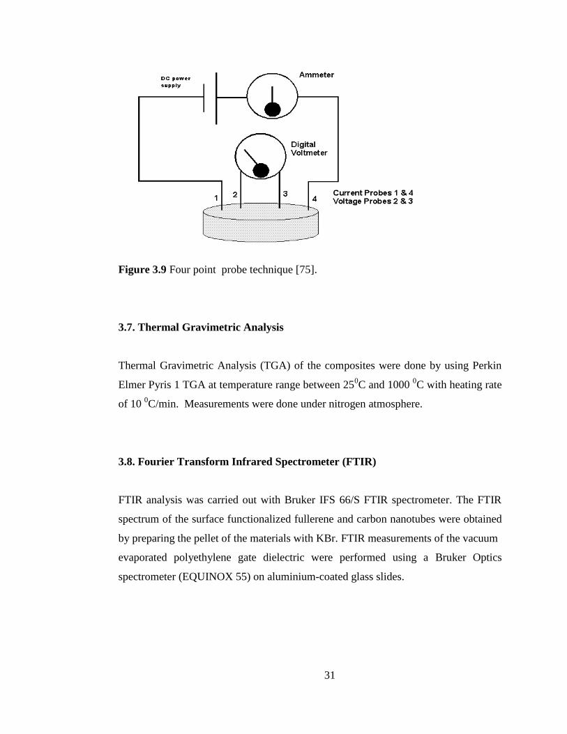
31
Figure 3.9 Four point probe technique [75].
3.7. Thermal Gravimetric Analysis
Thermal Gravimetric Analysis (TGA) of the composites were done by using Perkin
Elmer Pyris 1 TGA at temperature range between 250C and 1000
0C with heating rate
of 10 0C/min. Measurements were done under nitrogen atmosphere.
3.8. Fourier Transform Infrared Spectrometer (FTIR)
FTIR analysis was carried out with Bruker IFS 66/S FTIR spectrometer. The FTIR
spectrum of the surface functionalized fullerene and carbon nanotubes were obtained
by preparing the pellet of the materials with KBr. FTIR measurements of the vacuum
evaporated polyethylene gate dielectric were performed using a Bruker Optics
spectrometer (EQUINOX 55) on aluminium-coated glass slides.
32
3.9. Differential Scanning Calorimetry
Thermal properties of composites were studied with Dupont Thermal Analyst 2000
DSC 910S instrument at the temperature range between 25 0C - 225
0C under N2
atmosphere. Heating rate was 5 0C /min. Percent crystallinities were calculated from
the peak areas.
3.10. Scanning Electron Microscopy (SEM)
The morphological studies of the samples were performed by FEI Quanta 400 F
Scanning Electron Microscopy. SEM micrographs of the fracture surfaces of
composites were obtained at different magnifications. The fracture surfaces of the
samples were coated by a thin layer of gold before investigation. The aim of this
study was to observe dispersion of Carbon Black, Fullerene and Carbon nanotube
particles in PP matrix
3.11. X Ray Photoelectron Spectroscopy (XPS)
X ray photoelectron spectroscopy was used to confirm the surface functionalization
of the carbon nanotubes. XPS analyses of the samples were done by using Mg K
Alpha source.
3.12. Zeta Potential
Surface charge of the surface modified and non modified carbon nanotube and
fullerene samples were determined with zeta potential measurement. Zeta potentials
of the samples were measured by using MALVERN Nano ZS90.
33
3.13. Transmission Electron Microscopy
TEM analyses of the samples were done by using a JEOL-JSM 1220 Transmission
electron microscopy. Solutions of surface functionalized fullerene and carbon
nanotube were preperad in water and then the drop of the solution applied on gold
grid.
3.14. Tensile Test
Tensile tests were performed with Lloyd LR 30 K universal tensile testing machine
according to ASTM D638 (Standard Test Method for Tensile Properties of Plastics).
Crosshead speeds for injection molded and compression molded samples were 5
cm/min and 6.5 cm/min, respectively. Dog bone shaped molded samples were used
and measurements were done at 24 0C. 5 kN load cell was used in the measurements.
3.15.Impact Test
Charpy impact test (unnotched) were done by using Pendulum Impact Tester of
Coesfield Material Test machine. The test specimens were prepared by injection
molding. Bar shaped specimens having size 5.5 cm were used in the experiments.
3.16.Melt Flow Index
Melt flow property measurements were performed by using Coesfield Material Test,
Meltfixer LT. The measurement were done at 210 0C. Materials were allowed to melt
for 5 minutes. Then standard weight (2.16 kg) placed on the piston of the instrument
34
to compress the sample. After that, the weight of the flow sample was reported for 10
minutes.
3.17. Organic Field Effect Transistor Preparation
3.17.1. Preparation of Glass Substrate and Gate Electrode
Glass substrates (15mm x 15mm) were cleaned by using ammonia solution (25%
supplied from Merck) and hydrogen peroxide (30% supplied from Merck) in
ultrasonic bath at 80 0C for 15 minutes. Aluminum gate electrodes were prepared by
using shadow mask on clean glass substrate. The structure of the gate masks were
given in Figure 3.10. Aluminum evaporation was carried out with metal evaporator at
0.5-2 nm/sec evaporation rate under pressure 2x10⁻⁶
mbar.
Figure 3.10 Structure of gate mask
35
3.17.2. Aluminum Oxide (Alox) Preparation
Al2O3 gate insulator was prepared by anodization of aluminium gate immersed into
citric acid solution which is 0.01 M. Steel electrode was used as counter electrode.
Current density for the anodization was 0.06 mA/cm2. After anodization, gate
electrodes were washed with distilled water and dried at 180 0C two hours under
reduced pressure to get rid of water residues. The thickness of the Al2O3 layer is
proportional with the applied voltage. Experimental set up for Al2O3 preparation was
given in Figure 3.11.
Figure 3.11 Preparation of Al2O3 insulator layer
3.17.3. Evaporation of Low Density Polyethylene
Evaporation of Low Density Polyethylene was done with Edwards High Vacuum
System (Figure 3.12) at pressure of 10-6
torr with evaporation rate of 0.02-0.04
nm/sec. Dielectric layers with different thickness were deposited on gate electrodes.
36
Figure 3.12 Edwards organic evaporator
3.17.4. Evaporation of C60 and Pentacene
Semiconductor layers C60 and pentacene were prepared with Edwards High Vacuum
System at vacuum (Figure 3.12). Pentacene (normal grade, carbon ≥ 93.5 %) and C60
(sublimation grade, 99.9%) were supplied by Sigma–Aldrich and MER corporation,
respectively. The thickness of the deposited semiconductor layers were 100 nm.
Semiconductor layers of C60 and pentacene were deposited at pressure of 10-6
torr
with deposition rates of 0.05-0.1 nm/sec and 0.1-0.2 nm/sec, respectively.
3.17.5. Evaporation of Source and Drain electrode
Source and drain electrode were prepared by using shadow masks. Aluminum source
and drain electrodes were deposited for the transistors which have C60 semiconductor
37
layer. For the transistors which have pentacene semiconductor layer, Au source and
drain electrodes were evaporated. The masks with different channel lengths were
used in device fabrication. Structure of source and drain masks were given in Figure
3.13.
Figure 3.13 Structure of source - drain mask
3.17.6. OFET Characterization
Steady state current voltage measurements were performed with Agilent E5273 A
(Figure 3.14) instrument. A picture of transistor measurement set up was given in
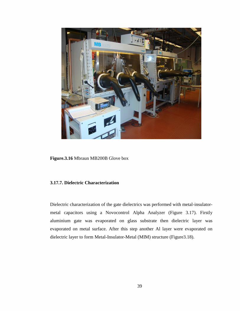
Figure 3.15. All measurements were done in Mbraun MB200B glove box.
38
Figure 3.14 Agilent 5273 A Transistor Measurement Device
Figure 3.15 Transistor measurement set up
39
Figure.3.16 Mbraun MB200B Glove box
3.17.7. Dielectric Characterization
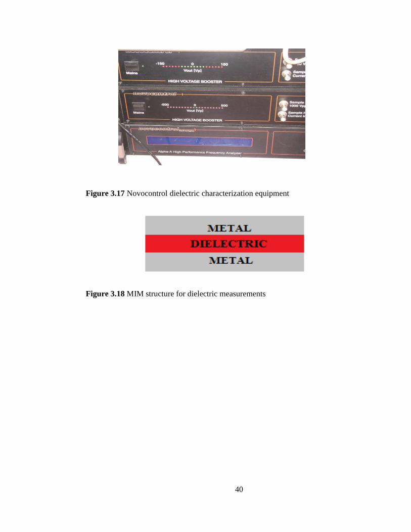
Dielectric characterization of the gate dielectrics was performed with metal-insulator-
metal capacitors using a Novocontrol Alpha Analyzer (Figure 3.17). Firstly
aluminium gate was evaporated on glass substrate then dielectric layer was
evaporated on metal surface. After this step another Al layer were evaporated on
dielectric layer to form Metal-Insulator-Metal (MIM) structure (Figure3.18).
40
Figure 3.17 Novocontrol dielectric characterization equipment
Figure 3.18 MIM structure for dielectric measurements
41
CHAPTER 4
RESULTS AND DISCUSSION
Results and discussion part of this dissertation is separated into six main parts.
Properties of Polypropylene/Carbon Black composites were discussed in the first
part. Characterization of surface functionalized carbon nanotubes and fullerenes were
given in second and third part, respectively. Fourth and fifth parts include the
properties of Polypropylene/Carbon Nanotube and Polypropylene/Fullerene
composites, respectively. The last part describes device characteristics of the
transistor which are built with the polyethylene gate dielectric.
4.1. Polypropylene / Carbon Black Composites
4.1.1 Melt Flow Index
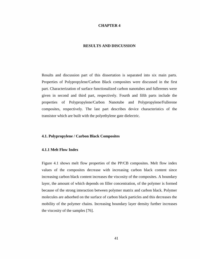
Figure 4.1 shows melt flow properties of the PP/CB composites. Melt flow index
values of the composites decrease with increasing carbon black content since
increasing carbon black content increases the viscosity of the composites. A boundary
layer, the amount of which depends on filler concentration, of the polymer is formed
because of the strong interaction between polymer matrix and carbon black. Polymer
molecules are adsorbed on the surface of carbon black particles and this decreases the
mobility of the polymer chains. Increasing boundary layer density further increases
the viscosity of the samples [76].
42
Figure 4.1 Melt flow properties of PP/CB composites
4.1.2. Percent Crystallinity of PP/CB composites
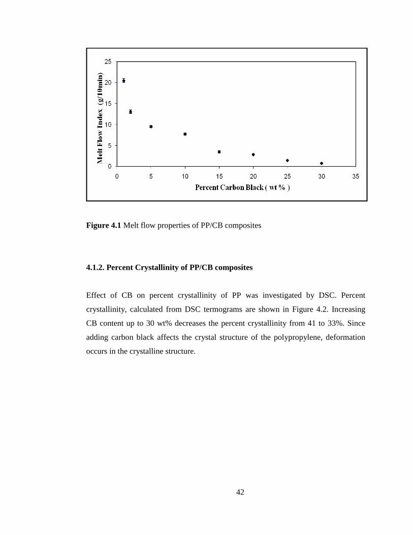
Effect of CB on percent crystallinity of PP was investigated by DSC. Percent
crystallinity, calculated from DSC termograms are shown in Figure 4.2. Increasing
CB content up to 30 wt% decreases the percent crystallinity from 41 to 33%. Since
adding carbon black affects the crystal structure of the polypropylene, deformation
occurs in the crystalline structure.
43
Figure 4.2 Percent crystallinity of the PP/CB composites
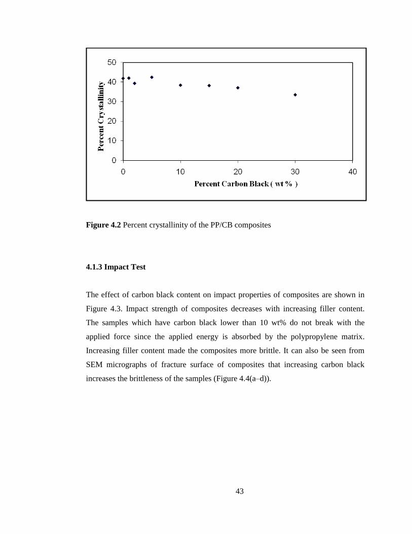
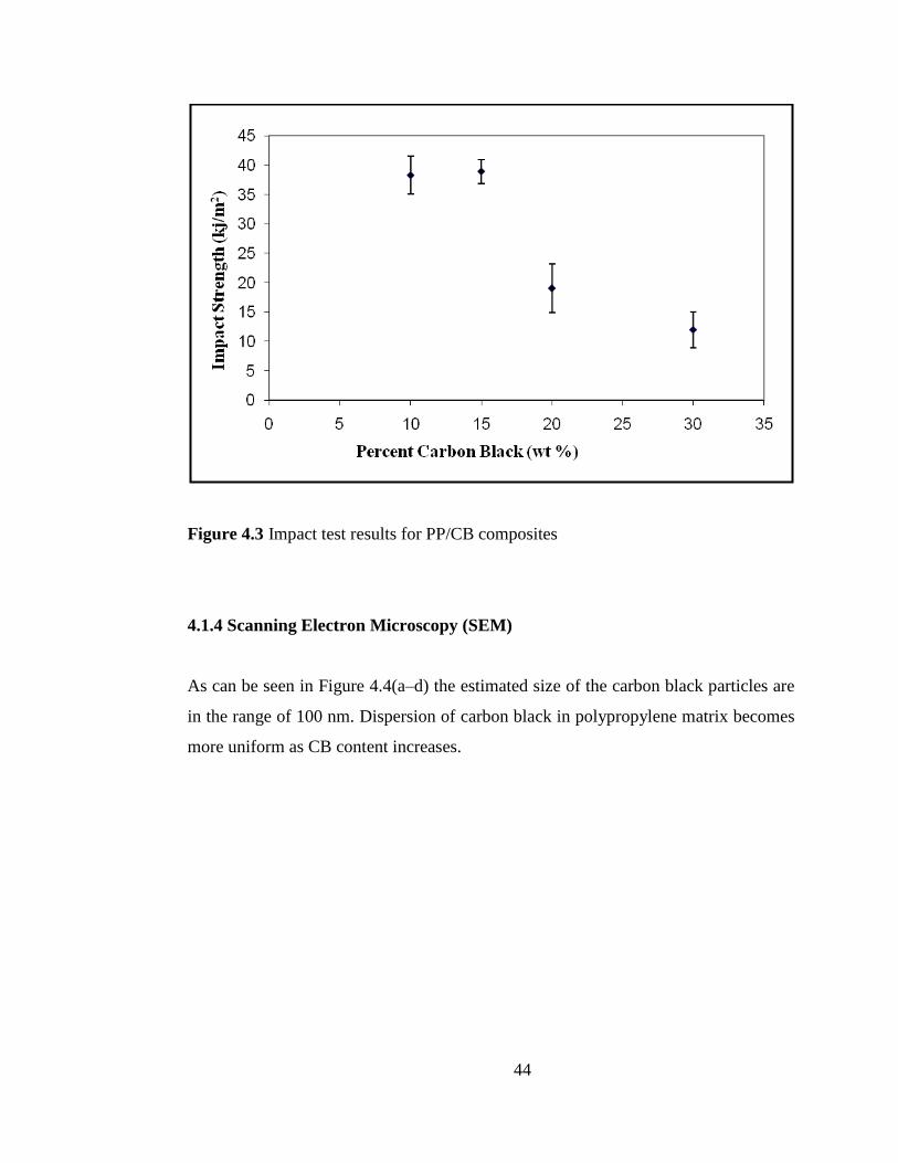
4.1.3 Impact Test
The effect of carbon black content on impact properties of composites are shown in
Figure 4.3. Impact strength of composites decreases with increasing filler content.
The samples which have carbon black lower than 10 wt% do not break with the
applied force since the applied energy is absorbed by the polypropylene matrix.
Increasing filler content made the composites more brittle. It can also be seen from
SEM micrographs of fracture surface of composites that increasing carbon black
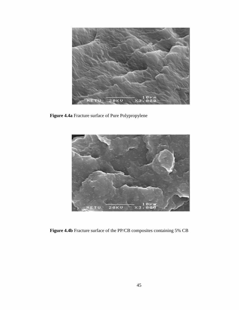
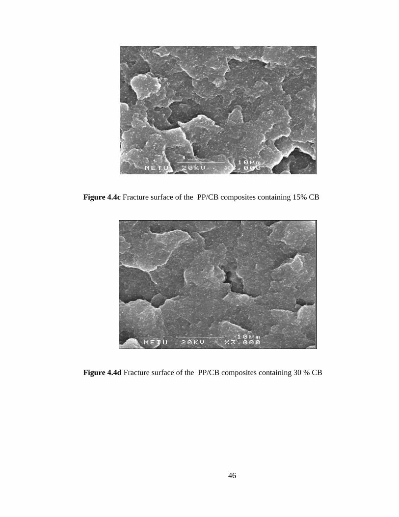
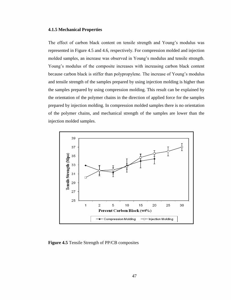
increases the brittleness of the samples (Figure 4.4(a–d)).
44
Figure 4.3 Impact test results for PP/CB composites
4.1.4 Scanning Electron Microscopy (SEM)
As can be seen in Figure 4.4(a–d) the estimated size of the carbon black particles are
in the range of 100 nm. Dispersion of carbon black in polypropylene matrix becomes
more uniform as CB content increases.
45
Figure 4.4a Fracture surface of Pure Polypropylene
Figure 4.4b Fracture surface of the PP/CB composites containing 5% CB
46
Figure 4.4c Fracture surface of the PP/CB composites containing 15% CB
Figure 4.4d Fracture surface of the PP/CB composites containing 30 % CB
47
4.1.5 Mechanical Properties
The effect of carbon black content on tensile strength and Young‟s modulus was
represented in Figure 4.5 and 4.6, respectively. For compression molded and injection
molded samples, an increase was observed in Young‟s modulus and tensile strength.
Young‟s modulus of the composite increases with increasing carbon black content
because carbon black is stiffer than polypropylene. The increase of Young‟s modulus
and tensile strength of the samples prepared by using injection molding is higher than
the samples prepared by using compression molding. This result can be explained by
the orientation of the polymer chains in the direction of applied force for the samples
prepared by injection molding. In compression molded samples there is no orientation
of the polymer chains, and mechanical strength of the samples are lower than the
injection molded samples.
Figure 4.5 Tensile Strength of PP/CB composites
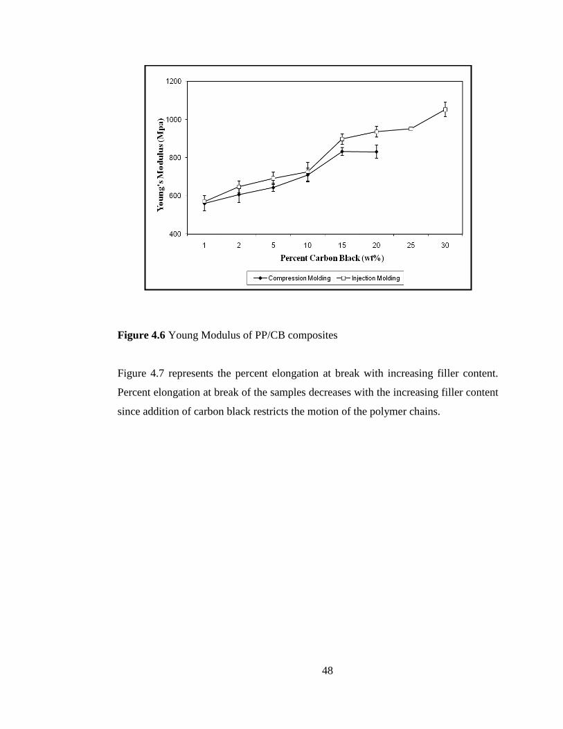
48
Figure 4.6 Young Modulus of PP/CB composites
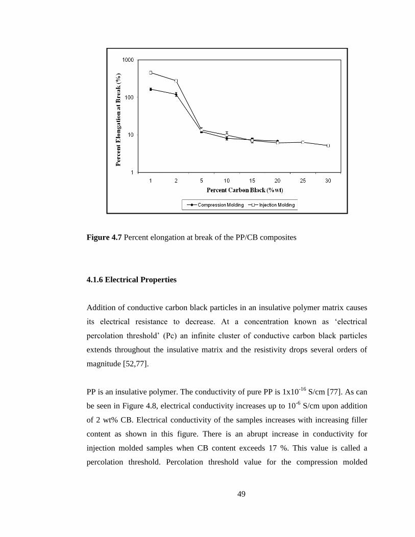
Figure 4.7 represents the percent elongation at break with increasing filler content.
Percent elongation at break of the samples decreases with the increasing filler content
since addition of carbon black restricts the motion of the polymer chains.
49
Figure 4.7 Percent elongation at break of the PP/CB composites
4.1.6 Electrical Properties
Addition of conductive carbon black particles in an insulative polymer matrix causes
its electrical resistance to decrease. At a concentration known as „electrical
percolation threshold‟ (Pc) an infinite cluster of conductive carbon black particles
extends throughout the insulative matrix and the resistivity drops several orders of
magnitude [52,77].
PP is an insulative polymer. The conductivity of pure PP is 1x10-16
S/cm [77]. As can
be seen in Figure 4.8, electrical conductivity increases up to 10-6
S/cm upon addition
of 2 wt% CB. Electrical conductivity of the samples increases with increasing filler
content as shown in this figure. There is an abrupt increase in conductivity for
injection molded samples when CB content exceeds 17 %. This value is called a
percolation threshold. Percolation threshold value for the compression molded
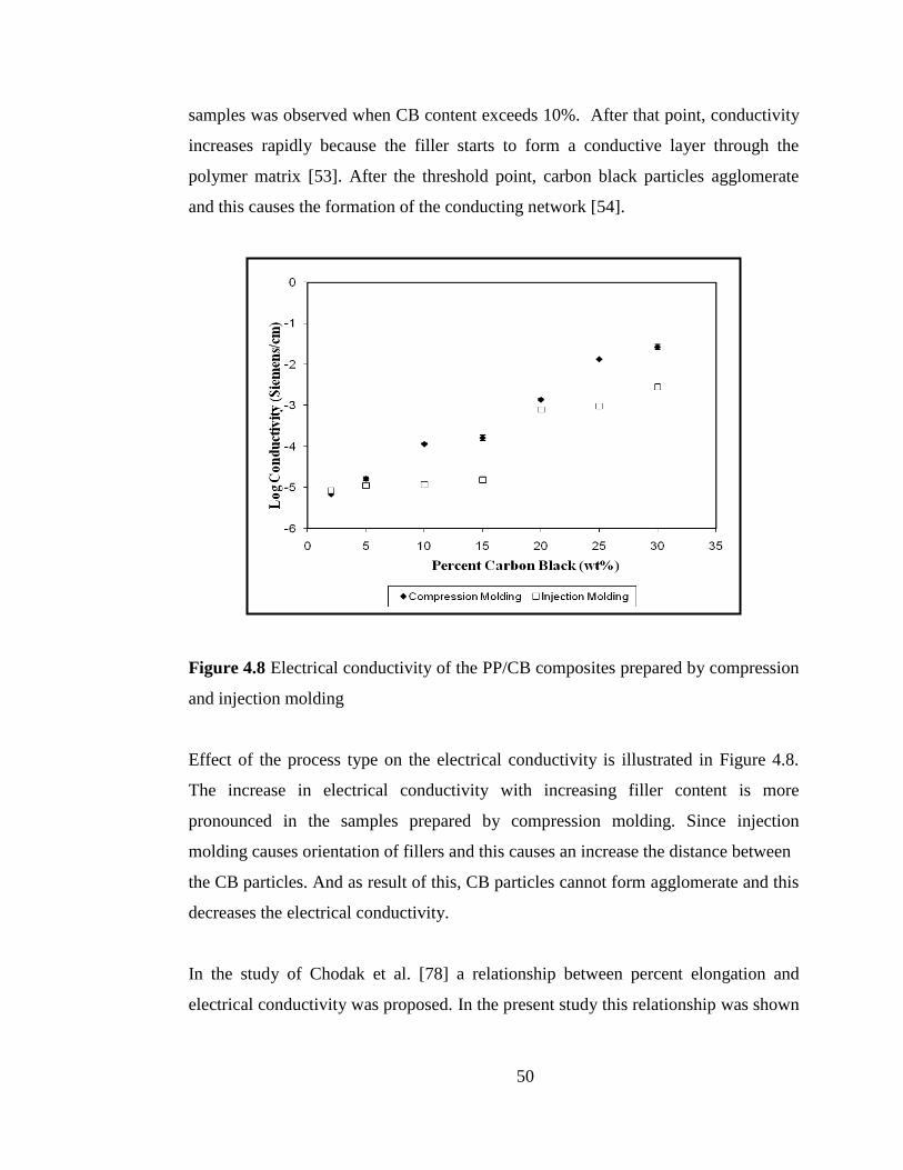
50
samples was observed when CB content exceeds 10%. After that point, conductivity
increases rapidly because the filler starts to form a conductive layer through the
polymer matrix [53]. After the threshold point, carbon black particles agglomerate
and this causes the formation of the conducting network [54].
Figure 4.8 Electrical conductivity of the PP/CB composites prepared by compression
and injection molding
Effect of the process type on the electrical conductivity is illustrated in Figure 4.8.
The increase in electrical conductivity with increasing filler content is more
pronounced in the samples prepared by compression molding. Since injection
molding causes orientation of fillers and this causes an increase the distance between
the CB particles. And as result of this, CB particles cannot form agglomerate and this
decreases the electrical conductivity.
In the study of Chodak et al. [78] a relationship between percent elongation and
electrical conductivity was proposed. In the present study this relationship was shown
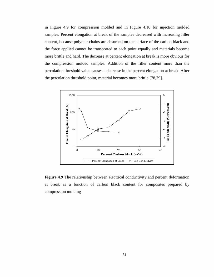
51
in Figure 4.9 for compression molded and in Figure 4.10 for injection molded
samples. Percent elongation at break of the samples decreased with increasing filler
content, because polymer chains are absorbed on the surface of the carbon black and
the force applied cannot be transported to each point equally and materials become
more brittle and hard. The decrease at percent elongation at break is more obvious for
the compression molded samples. Addition of the filler content more than the
percolation threshold value causes a decrease in the percent elongation at break. After
the percolation threshold point, material becomes more brittle [78,79].
Figure 4.9 The relationship between electrical conductivity and percent deformation
at break as a function of carbon black content for composites prepared by
compression molding
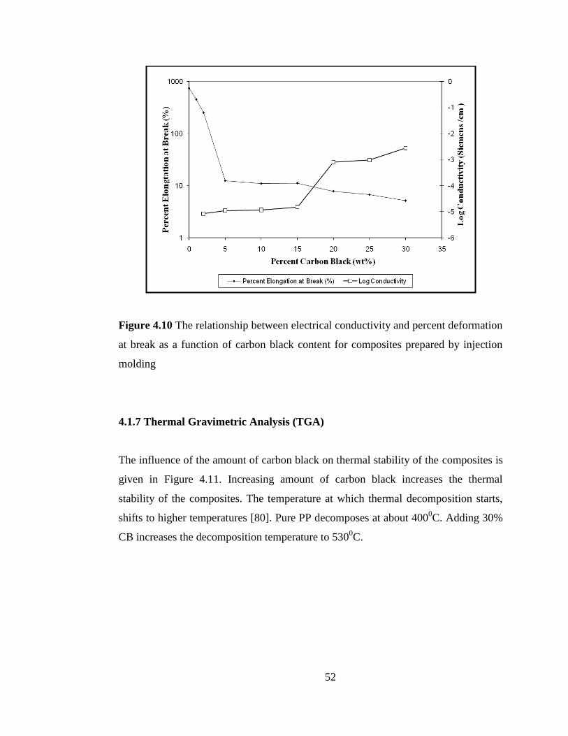
52
Figure 4.10 The relationship between electrical conductivity and percent deformation
at break as a function of carbon black content for composites prepared by injection
molding
4.1.7 Thermal Gravimetric Analysis (TGA)
The influence of the amount of carbon black on thermal stability of the composites is
given in Figure 4.11. Increasing amount of carbon black increases the thermal
stability of the composites. The temperature at which thermal decomposition starts,
shifts to higher temperatures [80]. Pure PP decomposes at about 4000C. Adding 30%
CB increases the decomposition temperature to 5300C.
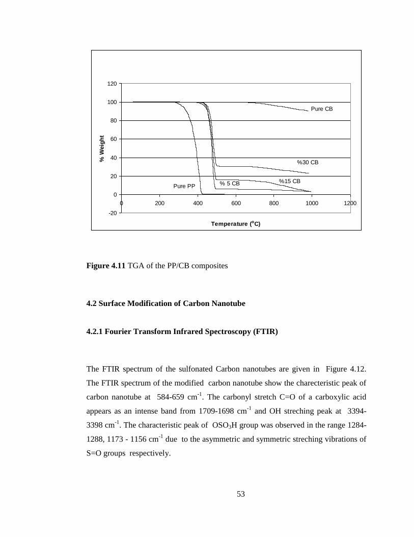
53
Figure 4.11 TGA of the PP/CB composites
4.2 Surface Modification of Carbon Nanotube
4.2.1 Fourier Transform Infrared Spectroscopy (FTIR)
The FTIR spectrum of the sulfonated Carbon nanotubes are given in Figure 4.12.
The FTIR spectrum of the modified carbon nanotube show the charecteristic peak of
carbon nanotube at 584-659 cm-1
. The carbonyl stretch C=O of a carboxylic acid
appears as an intense band from 1709-1698 cm-1
and OH streching peak at 3394-
3398 cm-1
. The characteristic peak of OSO3H group was observed in the range 1284-
1288, 1173 - 1156 cm-1
due to the asymmetric and symmetric streching vibrations of
S=O groups respectively.
-20
0
20
40
60
80
100
120
0 200 400 600 800 1000 1200
Temperature (oC)
% W
eig
ht
Pure CB
%30 CB
%15 CB% 5 CBPure PP
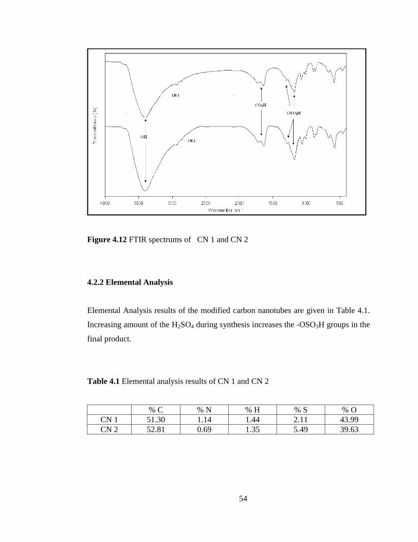
54
Figure 4.12 FTIR spectrums of CN 1 and CN 2
4.2.2 Elemental Analysis
Elemental Analysis results of the modified carbon nanotubes are given in Table 4.1.
Increasing amount of the H2SO4 during synthesis increases the -OSO3H groups in the
final product.
Table 4.1 Elemental analysis results of CN 1 and CN 2
% C % N % H % S % O
CN 1 51.30 1.14 1.44 2.11 43.99
CN 2 52.81 0.69 1.35 5.49 39.63
55
4.2.3 Electrical Conductivity
Electrical conductivity of untreated CN and surface modified ones are given in Table
4.2. As can be seen from this table increasing the sulphuric acid content during
modification of the material increases the electrical conductivity of the materials due
to higher acidic conductivity of hydrogensulfate content on surface [81].
Table 4.2 Electrical conductivity of Untreated CN, CN 1 and CN 2
Electrical Conductivity (S/cm)
Untreated CN 4.2 x 10⁻³
CN 1 2.1 x 10⁻²
CN 2 1.2 x 10⁻¹
4.2.4 X Ray Photoelectron Spectroscopy (XPS)
X ray photoelectron spectroscopy is used to confirm the surface functionalization of
the carbon nanotubes. XPS analyses of the samples were done by using Mg K Alpha
source. XPS spectra of the samples clearly show the existence of the functional
groups on the materials. Figure 4.13 and 4.14 show the XPS spectra of the materials.
The peaks coming from the 2p orbital of the sulfur are observed between 168-173
eV. These peaks show that the successive surface functionalization of the material
with -OSO3H groups. The peaks due to carboxylic acid and hydroxyl groups give
peak around ( O 1s) 530-536 eV and ( C 1s ) 282-288 eV, respectively.
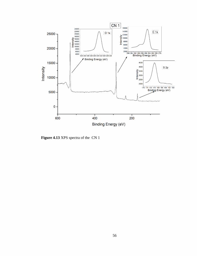
56
Figure 4.13 XPS spectra of the CN 1
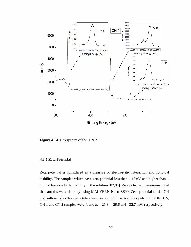
57
Figure 4.14 XPS spectra of the CN 2
4.2.5 Zeta Potential
Zeta potential is considered as a measure of electrostatic interaction and colloidal
stability. The samples which have zeta potential less than – 15mV and higher than +
15 mV have colloidal stability in the solution [82,83]. Zeta potential measurements of
the samples were done by using MALVERN Nano ZS90. Zeta potential of the CN
and sulfonated carbon nanotubes were measured in water. Zeta potential of the CN,
CN 1 and CN 2 samples were found as – 29.3, – 29.6 and - 32.7 mV, respectively.
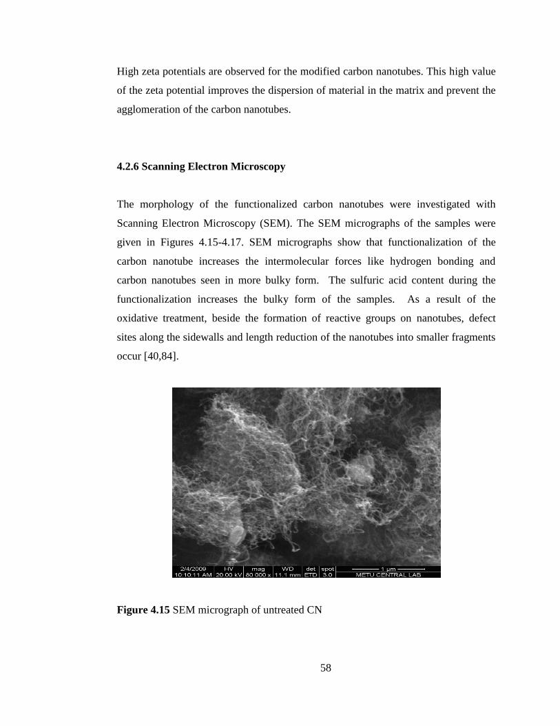
58
High zeta potentials are observed for the modified carbon nanotubes. This high value
of the zeta potential improves the dispersion of material in the matrix and prevent the
agglomeration of the carbon nanotubes.
4.2.6 Scanning Electron Microscopy
The morphology of the functionalized carbon nanotubes were investigated with
Scanning Electron Microscopy (SEM). The SEM micrographs of the samples were
given in Figures 4.15-4.17. SEM micrographs show that functionalization of the
carbon nanotube increases the intermolecular forces like hydrogen bonding and
carbon nanotubes seen in more bulky form. The sulfuric acid content during the
functionalization increases the bulky form of the samples. As a result of the
oxidative treatment, beside the formation of reactive groups on nanotubes, defect
sites along the sidewalls and length reduction of the nanotubes into smaller fragments
occur [40,84].
Figure 4.15 SEM micrograph of untreated CN
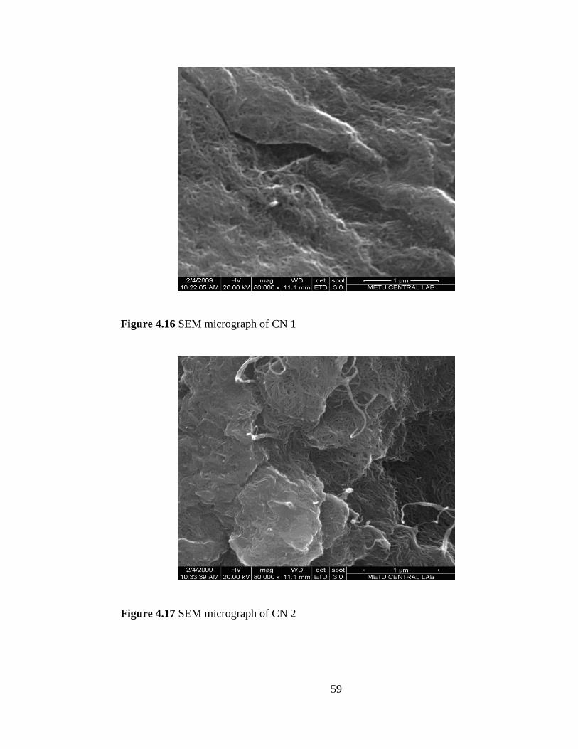
59
Figure 4.16 SEM micrograph of CN 1
Figure 4.17 SEM micrograph of CN 2
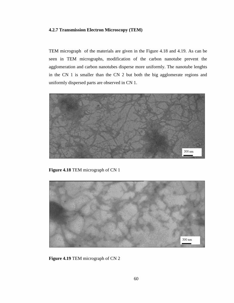
60
4.2.7 Transmission Electron Microscopy (TEM)
TEM micrograph of the materials are given in the Figure 4.18 and 4.19. As can be
seen in TEM micrographs, modification of the carbon nanotube prevent the
agglomeration and carbon nanotubes disperse more uniformly. The nanotube lenghts
in the CN 1 is smaller than the CN 2 but both the big agglomerate regions and
uniformly dispersed parts are observed in CN 1.
Figure 4.18 TEM micrograph of CN 1
Figure 4.19 TEM micrograph of CN 2
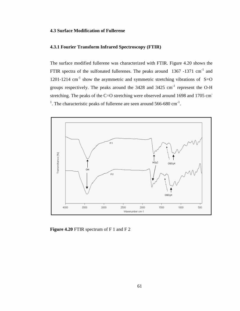
61
4.3 Surface Modification of Fullerene
4.3.1 Fourier Transform Infrared Spectroscopy (FTIR)
The surface modified fullerene was characterized with FTIR. Figure 4.20 shows the
FTIR spectra of the sulfonated fullerenes. The peaks around 1367 -1371 cm-1
and
1201-1214 cm-1
show the asymmetric and symmetric stretching vibrations of S=O
groups respectively. The peaks around the 3428 and 3425 cm-1
represent the O-H
stretching. The peaks of the C=O stretching were observed around 1698 and 1705 cm-
1. The characteristic peaks of fullerene are seen around 566-680 cm
-1.
Figure 4.20 FTIR spectrum of F 1 and F 2
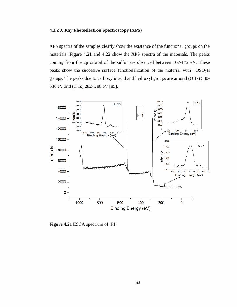
62
4.3.2 X Ray Photoelectron Spectroscopy (XPS)
XPS spectra of the samples clearly show the existence of the functional groups on the
materials. Figure 4.21 and 4.22 show the XPS spectra of the materials. The peaks
coming from the 2p orbital of the sulfur are observed between 167-172 eV. These
peaks show the succesive surface functionalization of the material with –OSO3H
groups. The peaks due to carboxylic acid and hydroxyl groups are around (O 1s) 530-
536 eV and (C 1s) 282- 288 eV [85].
Figure 4.21 ESCA spectrum of F1
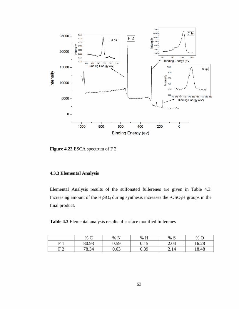
63
Figure 4.22 ESCA spectrum of F 2
4.3.3 Elemental Analysis
Elemental Analysis results of the sulfonated fullerenes are given in Table 4.3.
Increasing amount of the H2SO4 during synthesis increases the -OSO3H groups in the
final product.
Table 4.3 Elemental analysis results of surface modified fullerenes
% C % N % H % S % O
F 1 80.93 0.59 0.15 2.04 16.28
F 2 78.34 0.63 0.39 2.14 18.48
64
4.3.4 Electrical Conductivity
Electrical conductivities of the samples are given in Table 4.4. Four Point Probe
method was used for conductivity measurements. Increasing the sulphuric acid
content during modification of the material increases the electrical conductivity of the
materials due to higher acidic conductivity of hydrogensulfate content on surface
[81].
Table 4.4 Electrical Conductivity of the F1 and F2
4.3.5 Transmission Electron Microscopy
TEM micrographs of neat fullerene and modified fullerenes are given in Figures 4.23,
4.24 and 4.25 respectively. As can be seen from these figures modification of the
fullerene improves the dispersion in water and decreases the agglomeration. The
particle size is about 50-60 nm for surface modified fullerene (F2). The particle size
of the neat fullerene is about 80 nm.
Electrical Conductivity (S/cm)
F 1 1.78 x 10⁻²
F 2 2.72 x 10⁻²
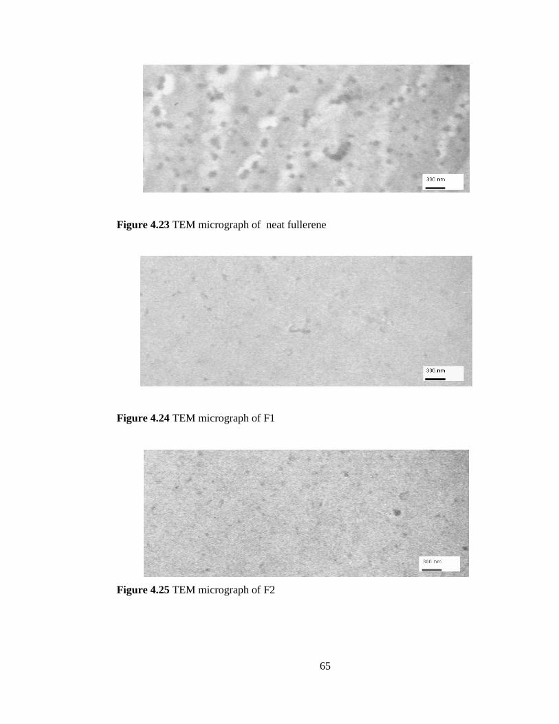
65
Figure 4.23 TEM micrograph of neat fullerene
Figure 4.24 TEM micrograph of F1
Figure 4.25 TEM micrograph of F2
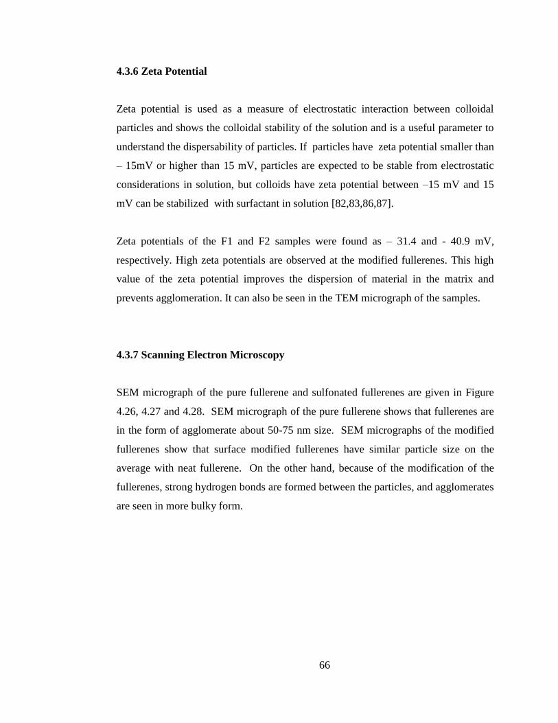
66
4.3.6 Zeta Potential
Zeta potential is used as a measure of electrostatic interaction between colloidal
particles and shows the colloidal stability of the solution and is a useful parameter to
understand the dispersability of particles. If particles have zeta potential smaller than
– 15mV or higher than 15 mV, particles are expected to be stable from electrostatic
considerations in solution, but colloids have zeta potential between –15 mV and 15
mV can be stabilized with surfactant in solution [82,83,86,87].
Zeta potentials of the F1 and F2 samples were found as – 31.4 and - 40.9 mV,
respectively. High zeta potentials are observed at the modified fullerenes. This high
value of the zeta potential improves the dispersion of material in the matrix and
prevents agglomeration. It can also be seen in the TEM micrograph of the samples.
4.3.7 Scanning Electron Microscopy
SEM micrograph of the pure fullerene and sulfonated fullerenes are given in Figure
4.26, 4.27 and 4.28. SEM micrograph of the pure fullerene shows that fullerenes are
in the form of agglomerate about 50-75 nm size. SEM micrographs of the modified
fullerenes show that surface modified fullerenes have similar particle size on the
average with neat fullerene. On the other hand, because of the modification of the
fullerenes, strong hydrogen bonds are formed between the particles, and agglomerates
are seen in more bulky form.
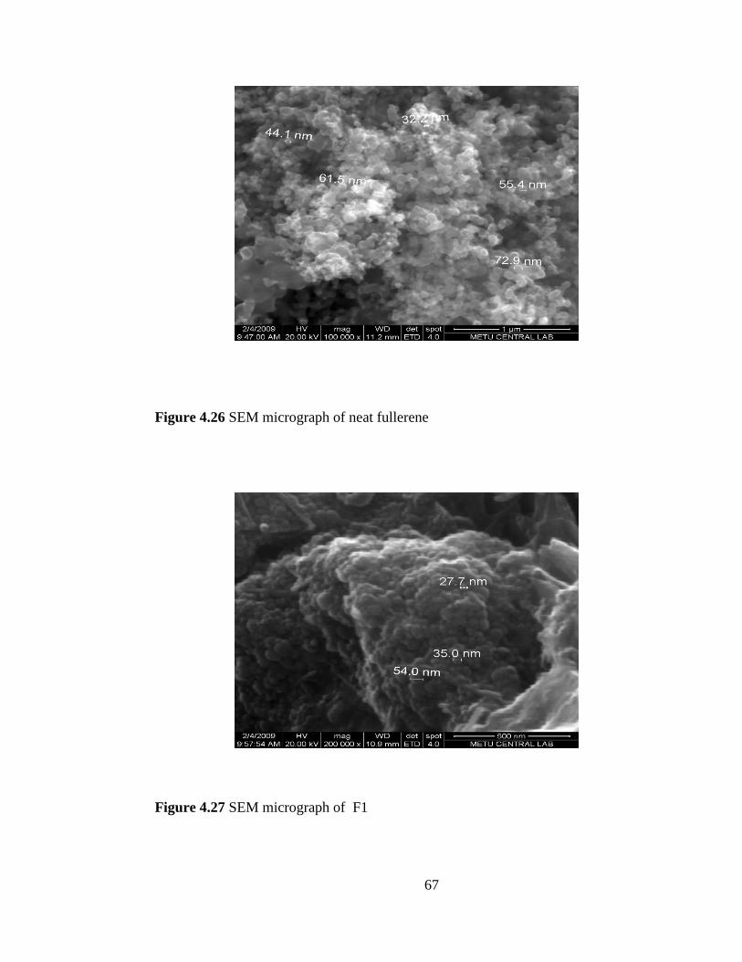
67
Figure 4.26 SEM micrograph of neat fullerene
Figure 4.27 SEM micrograph of F1
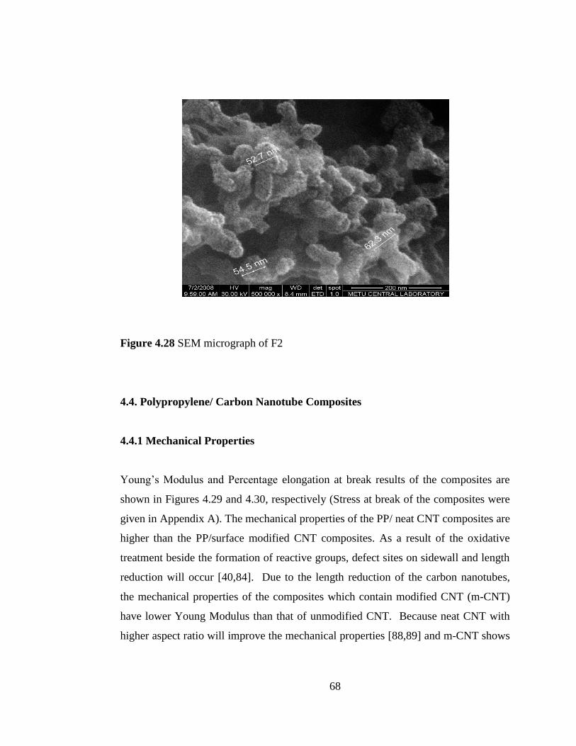
68
Figure 4.28 SEM micrograph of F2
4.4. Polypropylene/ Carbon Nanotube Composites
4.4.1 Mechanical Properties
Young‟s Modulus and Percentage elongation at break results of the composites are
shown in Figures 4.29 and 4.30, respectively (Stress at break of the composites were
given in Appendix A). The mechanical properties of the PP/ neat CNT composites are
higher than the PP/surface modified CNT composites. As a result of the oxidative
treatment beside the formation of reactive groups, defect sites on sidewall and length
reduction will occur [40,84]. Due to the length reduction of the carbon nanotubes,
the mechanical properties of the composites which contain modified CNT (m-CNT)
have lower Young Modulus than that of unmodified CNT. Because neat CNT with
higher aspect ratio will improve the mechanical properties [88,89] and m-CNT shows
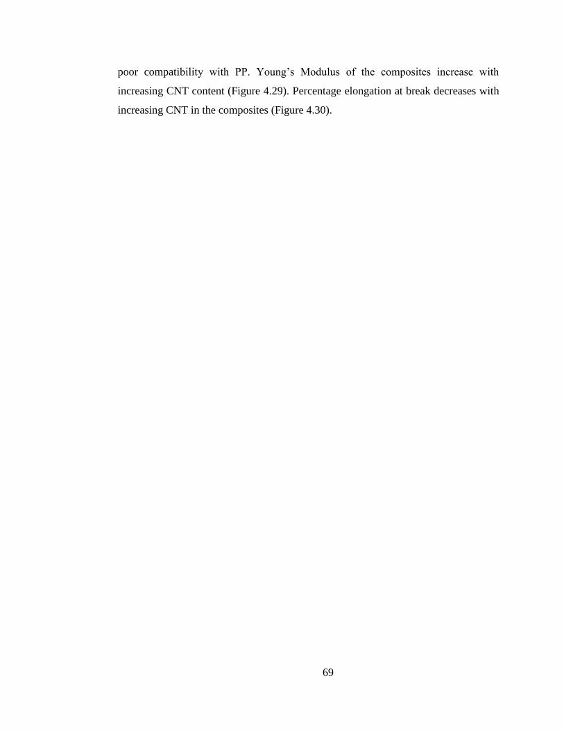
69
poor compatibility with PP. Young‟s Modulus of the composites increase with
increasing CNT content (Figure 4.29). Percentage elongation at break decreases with
increasing CNT in the composites (Figure 4.30).
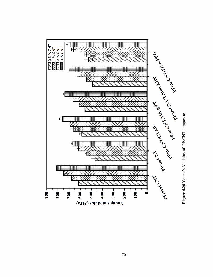
70
Fig
ure
4.2
9 Y
oung‟s M
odulus of PP/C
NT composites
71
Fig
ure
4.3
0 P
erce
nt
elongat
ion a
t bre
ak o
f P
P/C
NT
com
posi
tes
72
The highest mechanical strength and percent elongation at break were observed for
composites with MA-g-PP. MA-g-PP is one of the common compatibilizer for the PP
composites. Since MA-g-PP has similar backbone with polypropylene matrix and
similar functional groups with filler, it increases the compatibility of the filler in PP
matrix. Beside this, strong hydrogen bonding between m-CNT and MA-g-PP
promotes the compatibility of the m-CNT in polymer matrix. As a results of the MA-
g-PP addition percent elongation at break of the composites increased because MA-g-
PP is low molecular weight polymer and uncoiling of the MA-g-PP increases the
elongation during tensile test.
The composites which contain CTAB have high Young‟s modulus. CTAB have
hydrocarbon chain and positively charged end. Cationic ends of CTAB have good
interaction with the negatively charged CNT surface and hydrocarbon parts have
similar structure with the polymer matrix and this provides good dispersion in
polymer matrix. CTAB have no effect on percent elongation at break like MA-g-PP.
Sample which is prepared with CTAB showed brittle tensile behaviour.
Triton X 100 is a non ionic surfactant with hydrocarbon chain and carboxyl groups at
one end. Mechanical properties of the composites which are prepared with Triton X-
100 and PE-b-PEG are lower than the composites contain CTAB and MA-g-PP. The
composites which are prepared by using Triton X-100 and PE-b-PEG showed low
mechanical strength due to the poor adhesion of CNT with polymer matrix. Another
explanation for this result is the compatibilizers may function as plasticizer.
4.4.2 Electrical Conductivity
Electrical conductivity results are given in Figure 4.31. Electrical conductivities of
the composites were measured by using four probe technique. Electrical conductivity
of the composites increases with the CNT loading. Electrical conductivity of the
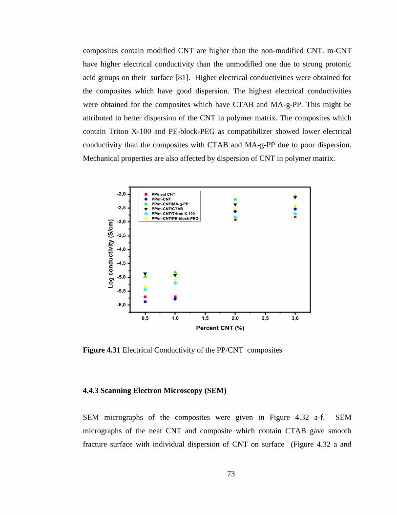
73
composites contain modified CNT are higher than the non-modified CNT. m-CNT
have higher electrical conductivity than the unmodified one due to strong protonic
acid groups on their surface [81]. Higher electrical conductivities were obtained for
the composites which have good dispersion. The highest electrical conductivities
were obtained for the composites which have CTAB and MA-g-PP. This might be
attributed to better dispersion of the CNT in polymer matrix. The composites which
contain Triton X-100 and PE-block-PEG as compatibilizer showed lower electrical
conductivity than the composites with CTAB and MA-g-PP due to poor dispersion.
Mechanical properties are also affected by dispersion of CNT in polymer matrix.
0,5 1,0 1,5 2,0 2,5 3,0
-6,0
-5,5
-5,0
-4,5
-4,0
-3,5
-3,0
-2,5
-2,0 PP/neat CNT
PP/m-CNT
PP/m-CNT/MA-g-PP
PP/m-CNT/CTAB
PP/m-CNT/Triton X-100
PP/m-CNT/PE-block-PEG
Lo
g c
on
du
cti
vit
y (
S/c
m)
Percent CNT (%)
Figure 4.31 Electrical Conductivity of the PP/CNT composites
4.4.3 Scanning Electron Microscopy (SEM)
SEM micrographs of the composites were given in Figure 4.32 a-f. SEM
micrographs of the neat CNT and composite which contain CTAB gave smooth
fracture surface with individual dispersion of CNT on surface (Figure 4.32 a and
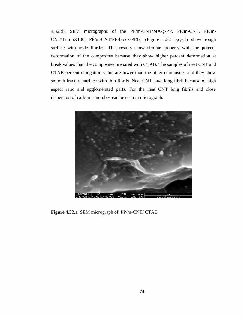
74
4.32.d). SEM micrographs of the PP/m-CNT/MA-g-PP, PP/m-CNT, PP/m-
CNT/TritonX100, PP/m-CNT/PE-block-PEG, (Figure 4.32 b,c,e,f) show rough
surface with wide fibriles. This results show similar property with the percent
deformation of the composites because they show higher percent deformation at
break values than the composites prepared with CTAB. The samples of neat CNT and
CTAB percent elongation value are lower than the other composites and they show
smooth fracture surface with thin fibrils. Neat CNT have long fibril because of high
aspect ratio and agglomerated parts. For the neat CNT long fibrils and close
dispersion of carbon nanotubes can be seen in micrograph.
Figure 4.32.a SEM micrograph of PP/m-CNT/ CTAB
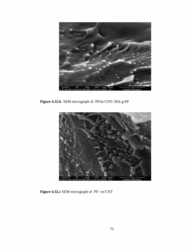
75
Figure 4.32.b SEM micrograph of PP/m-CNT/ MA-g-PP
Figure 4.32.c SEM micrograph of PP / m-CNT
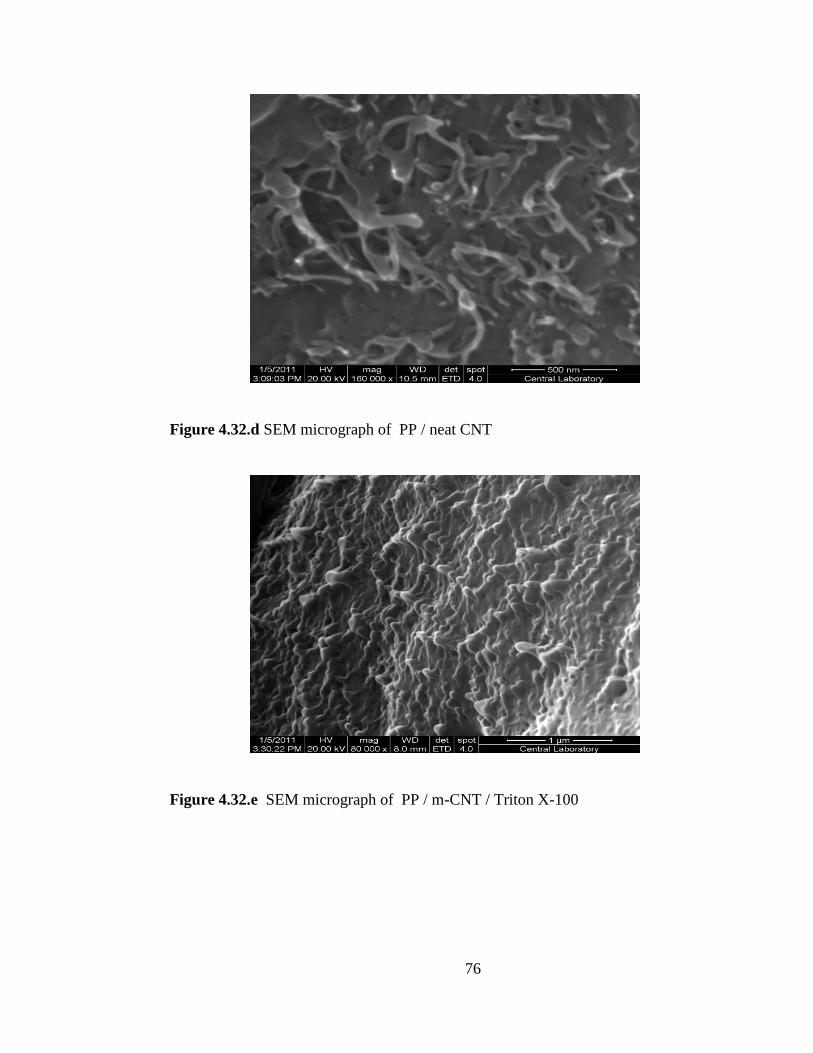
76
Figure 4.32.d SEM micrograph of PP / neat CNT
Figure 4.32.e SEM micrograph of PP / m-CNT / Triton X-100
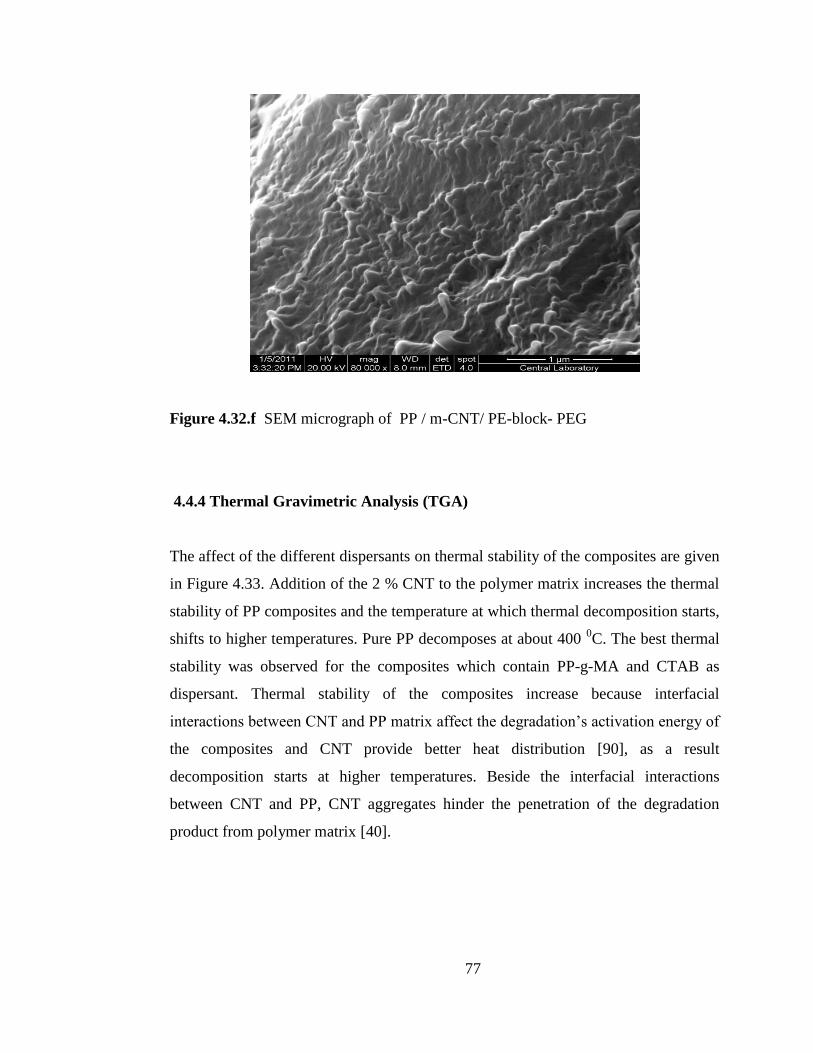
77
Figure 4.32.f SEM micrograph of PP / m-CNT/ PE-block- PEG
4.4.4 Thermal Gravimetric Analysis (TGA)
The affect of the different dispersants on thermal stability of the composites are given
in Figure 4.33. Addition of the 2 % CNT to the polymer matrix increases the thermal
stability of PP composites and the temperature at which thermal decomposition starts,
shifts to higher temperatures. Pure PP decomposes at about 400 0C. The best thermal
stability was observed for the composites which contain PP-g-MA and CTAB as
dispersant. Thermal stability of the composites increase because interfacial
interactions between CNT and PP matrix affect the degradation‟s activation energy of
the composites and CNT provide better heat distribution [90], as a result
decomposition starts at higher temperatures. Beside the interfacial interactions
between CNT and PP, CNT aggregates hinder the penetration of the degradation
product from polymer matrix [40].
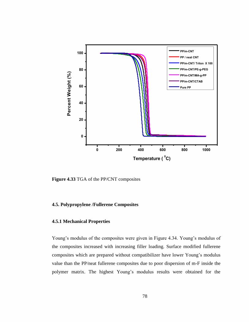
78
0 200 400 600 800 1000
0
20
40
60
80
100
Pe
rce
nt
We
igh
t (%
)
Temperature ( 0C)
PP/m-CNT
PP / neat CNT
PP/m-CNT/ Triton X 100
PP/m-CNT/PE-g-PEG
PP/m-CNT/MA-g-PP
PP/m-CNT/CTAB
Pure PP
Figure 4.33 TGA of the PP/CNT composites
4.5. Polypropylene /Fullerene Composites
4.5.1 Mechanical Properties
Young‟s modulus of the composites were given in Figure 4.34. Young‟s modulus of
the composites increased with increasing filler loading. Surface modified fullerene
composites which are prepared without compatibilizer have lower Young‟s modulus
value than the PP/neat fullerene composites due to poor dispersion of m-F inside the
polymer matrix. The highest Young‟s modulus results were obtained for the
79
composites which contain MA-g-PP and CTAB as dispersant. Addition of the MA-g-
PP as compatibilizer increased the mechanical properties of the composites because
its provides better dispersion of the fullerene particles inside the polymer matrix. Ma-
g-PP has similar structure with polymer matrix and similar functional groups with
surface modified fullerene particles. Strong hydrogen bonding occurs between
functional groups of fullerene and MA-g-PP and this promotes the compability of the
fullerene particles in polymer matrix.
Addition of the CTAB compatibilizer showed similar effect on Young‟s modulus like
MA-g-PP. Composites which are prepared with CTAB showed high Young modulus
because CTAB is cationic surfactant. Cationic ends of the CTAB and negatively
charged surface of the modified fullerene showed good interaction. As a result of the
good compatibility of CTAB and fullerene particles, fullerene particles showed good
dispersion in polymer matrix.
Young modulus of the composites which is prepared with PE-b-PEG and Triton X-
100 are close to the value of neat fullerene composites. Triton X 100 and PE-b-PEG
did not show any significant effect on Young Modulus of the composites.
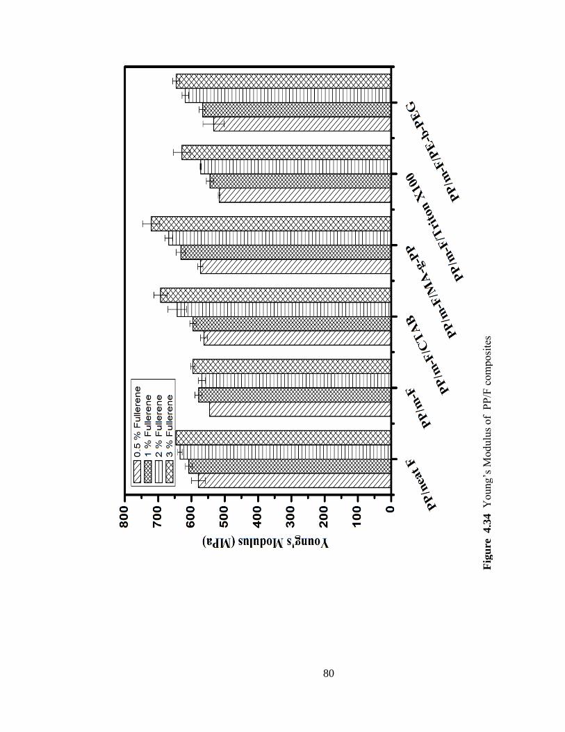
80
Fig
ure
4.3
4 Young‟s M
odulus of PP/F composites
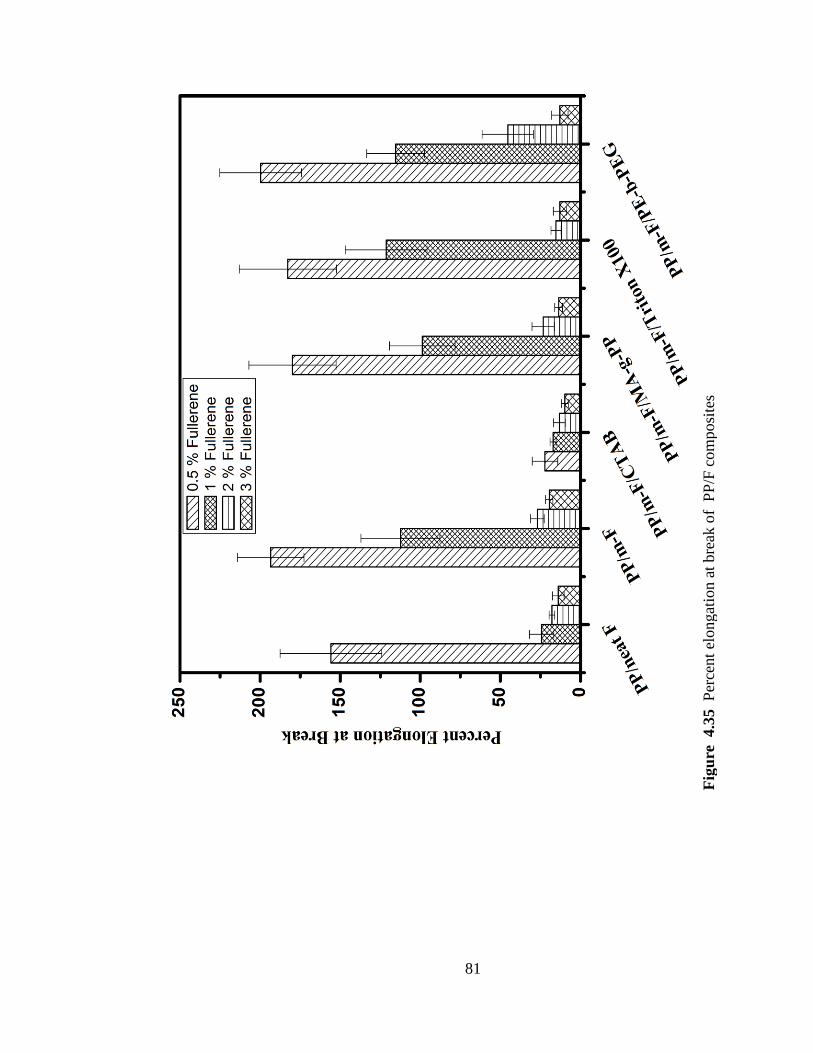
81
Fig
ure
4.3
5 P
erce
nt
elongat
ion a
t bre
ak o
f P
P/F
com
posi
tes
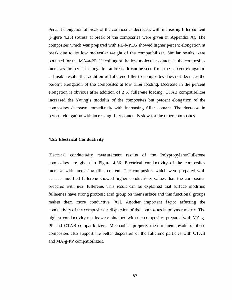
82
Percant elongation at break of the composites decreases with increasing filler content
(Figure 4.35) (Stress at break of the composites were given in Appendix A). The
composites which was prepared with PE-b-PEG showed higher percent elongation at
break due to its low molecular weight of the compatibilizer. Similar results were
obtained for the MA-g-PP. Uncoiling of the low molecular content in the composites
increases the percent elongation at break. It can be seen from the percent elongation
at break results that addition of fullerene filler to composites does not decrease the
percent elongation of the composites at low filler loading. Decrease in the percent
elongation is obvious after addition of 2 % fullerene loading. CTAB compatibilizer
increased the Young‟s modulus of the composites but percent elongation of the
composites decrease immediately with increasing filler content. The decrease in
percent elongation with increasing filler content is slow for the other composites.
4.5.2 Electrical Conductivity
Electrical conductivity measurement results of the Polypropylene/Fullerene
composites are given in Figure 4.36. Electrical conductivity of the composites
increase with increasing filler content. The composites which were prepared with
surface modified fullerene showed higher conductivity values than the composites
prepared with neat fullerene. This result can be explained that surface modified
fullerenes have strong protonic acid group on their surface and this functional groups
makes them more conductive [81]. Another important factor affecting the
conductivity of the composites is dispersion of the composites in polymer matrix. The
highest conductivity results were obtained with the composites prepared with MA-g-
PP and CTAB compatibilizers. Mechanical property measurement result for these
composites also support the better dispersion of the fullerene particles with CTAB
and MA-g-PP compatibilizers.
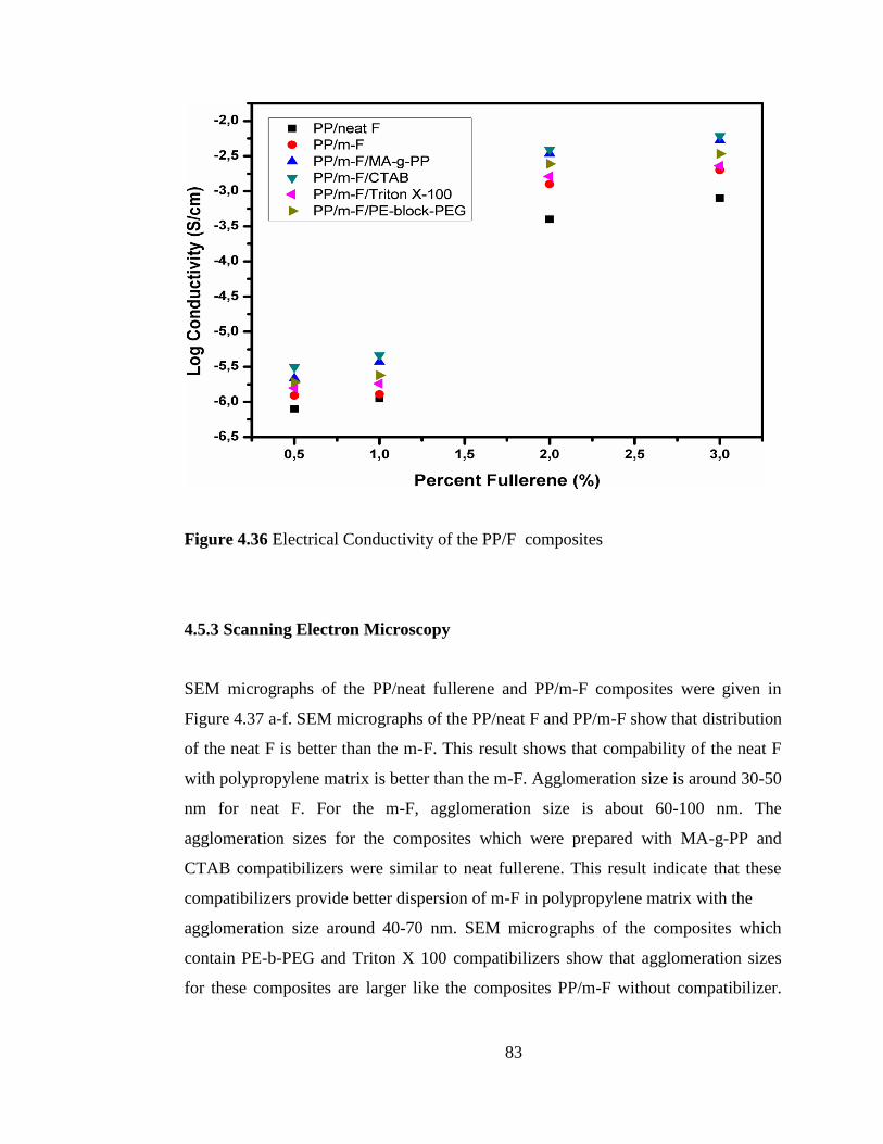
83
Figure 4.36 Electrical Conductivity of the PP/F composites
4.5.3 Scanning Electron Microscopy
SEM micrographs of the PP/neat fullerene and PP/m-F composites were given in
Figure 4.37 a-f. SEM micrographs of the PP/neat F and PP/m-F show that distribution
of the neat F is better than the m-F. This result shows that compability of the neat F
with polypropylene matrix is better than the m-F. Agglomeration size is around 30-50
nm for neat F. For the m-F, agglomeration size is about 60-100 nm. The
agglomeration sizes for the composites which were prepared with MA-g-PP and
CTAB compatibilizers were similar to neat fullerene. This result indicate that these
compatibilizers provide better dispersion of m-F in polypropylene matrix with the
agglomeration size around 40-70 nm. SEM micrographs of the composites which
contain PE-b-PEG and Triton X 100 compatibilizers show that agglomeration sizes
for these composites are larger like the composites PP/m-F without compatibilizer.
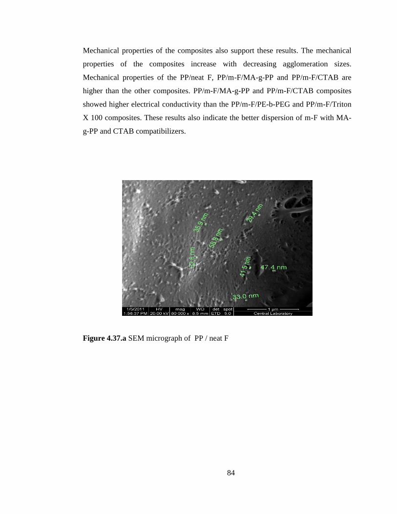
84
Mechanical properties of the composites also support these results. The mechanical
properties of the composites increase with decreasing agglomeration sizes.
Mechanical properties of the PP/neat F, PP/m-F/MA-g-PP and PP/m-F/CTAB are
higher than the other composites. PP/m-F/MA-g-PP and PP/m-F/CTAB composites
showed higher electrical conductivity than the PP/m-F/PE-b-PEG and PP/m-F/Triton
X 100 composites. These results also indicate the better dispersion of m-F with MA-
g-PP and CTAB compatibilizers.
Figure 4.37.a SEM micrograph of PP / neat F
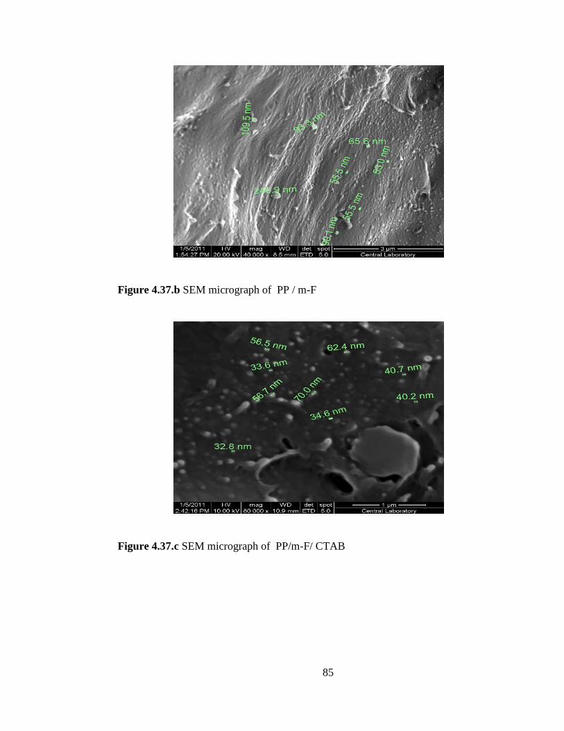
85
Figure 4.37.b SEM micrograph of PP / m-F
Figure 4.37.c SEM micrograph of PP/m-F/ CTAB
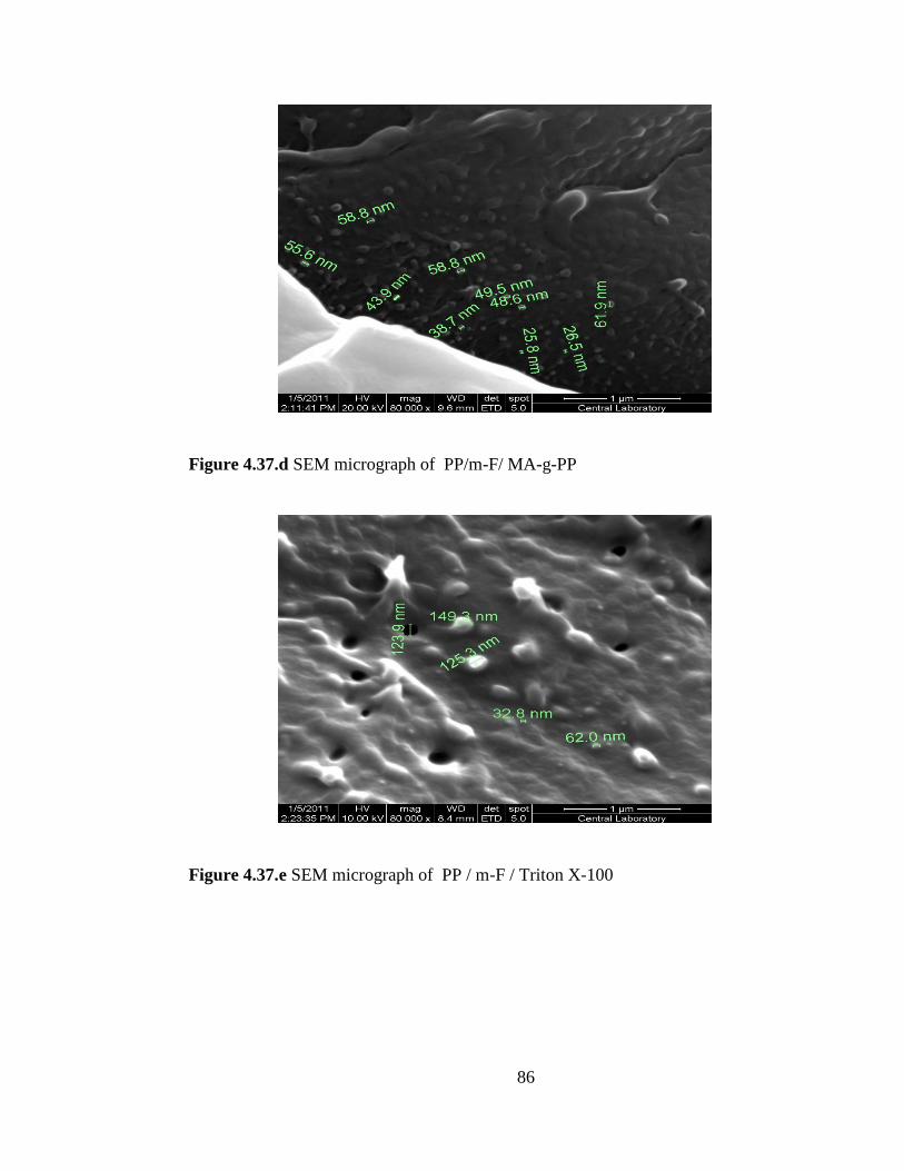
86
Figure 4.37.d SEM micrograph of PP/m-F/ MA-g-PP
Figure 4.37.e SEM micrograph of PP / m-F / Triton X-100
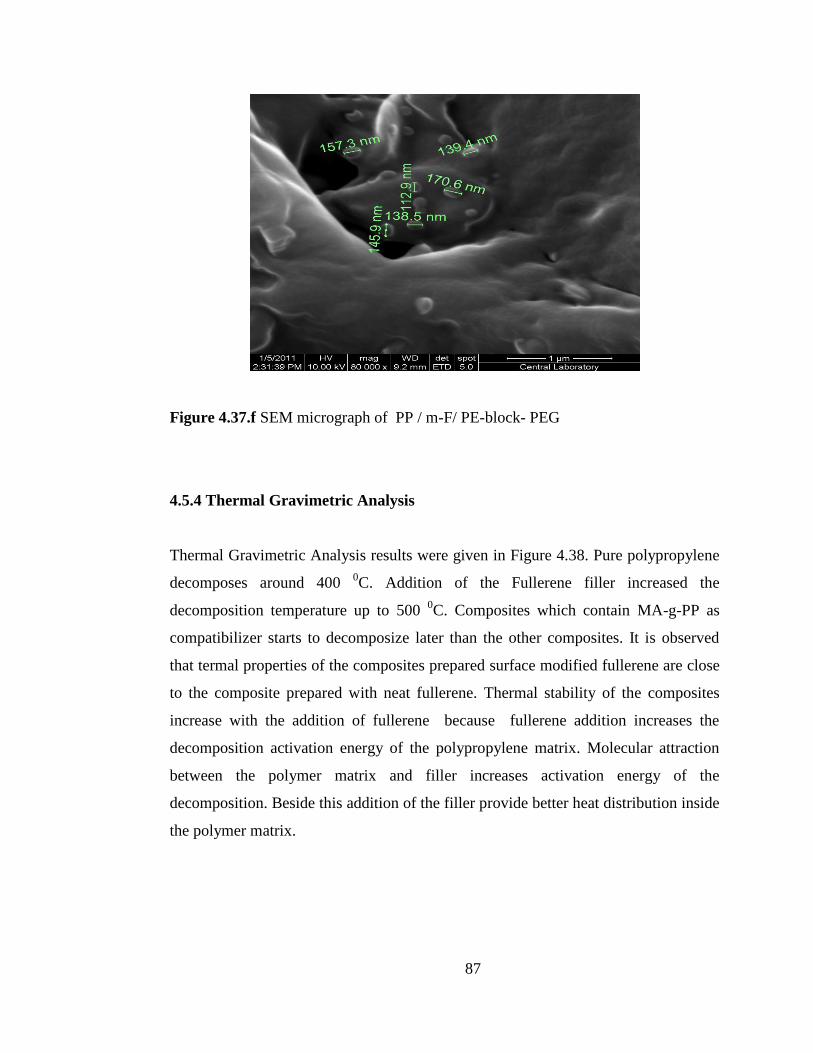
87
Figure 4.37.f SEM micrograph of PP / m-F/ PE-block- PEG
4.5.4 Thermal Gravimetric Analysis
Thermal Gravimetric Analysis results were given in Figure 4.38. Pure polypropylene
decomposes around 400 0C. Addition of the Fullerene filler increased the
decomposition temperature up to 500 0C. Composites which contain MA-g-PP as
compatibilizer starts to decomposize later than the other composites. It is observed
that termal properties of the composites prepared surface modified fullerene are close
to the composite prepared with neat fullerene. Thermal stability of the composites
increase with the addition of fullerene because fullerene addition increases the
decomposition activation energy of the polypropylene matrix. Molecular attraction
between the polymer matrix and filler increases activation energy of the
decomposition. Beside this addition of the filler provide better heat distribution inside
the polymer matrix.
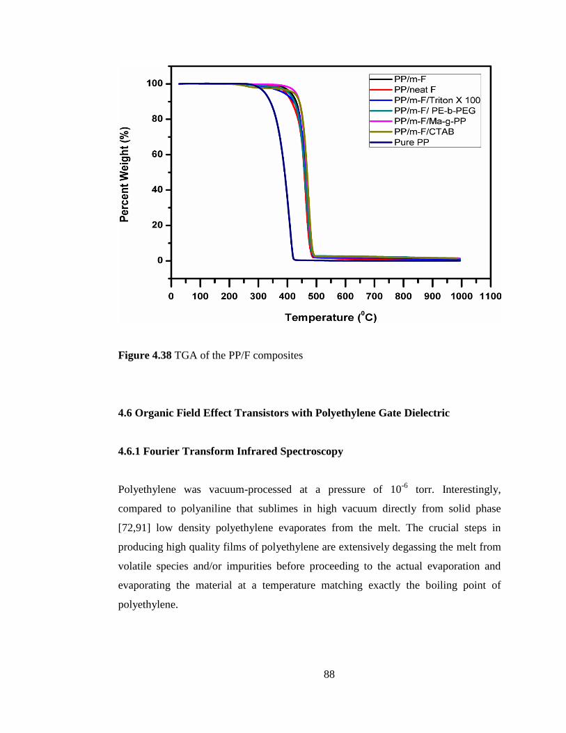
88
Figure 4.38 TGA of the PP/F composites
4.6 Organic Field Effect Transistors with Polyethylene Gate Dielectric
4.6.1 Fourier Transform Infrared Spectroscopy
Polyethylene was vacuum-processed at a pressure of 10-6
torr. Interestingly,
compared to polyaniline that sublimes in high vacuum directly from solid phase
[72,91] low density polyethylene evaporates from the melt. The crucial steps in
producing high quality films of polyethylene are extensively degassing the melt from
volatile species and/or impurities before proceeding to the actual evaporation and
evaporating the material at a temperature matching exactly the boiling point of
polyethylene.
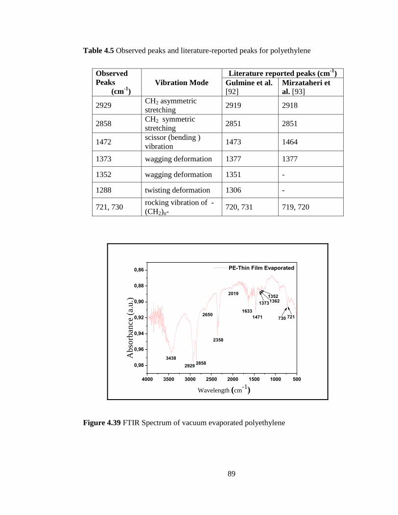
89
Table 4.5 Observed peaks and literature-reported peaks for polyethylene
Observed
Peaks
(cm-1
)
Vibration Mode
Literature reported peaks (cm-1
)
Gulmine et al.
[92] Mirzataheri et
al. [93]
2929 CH2 asymmetric
stretching 2919 2918
2858 CH2 symmetric
stretching 2851 2851
1472 scissor (bending )
vibration 1473 1464
1373 wagging deformation 1377 1377
1352 wagging deformation 1351 -
1288 twisting deformation 1306 -
721, 730 rocking vibration of -
(CH2)n- 720, 731 719, 720
4000 3500 3000 2500 2000 1500 1000 500
0,98
0,96
0,94
0,92
0,90
0,88
0,86
730
13621352
721
Ab
sorb
ance
(a.
u.)
Wavelength (cm-1)
3438
2019
2650
1373
1471
1633
29292858
2358
PE-Thin Film Evaporated
Figure 4.39 FTIR Spectrum of vacuum evaporated polyethylene

90
Fourier transform infrared spectra of vacuum-processed polyethylene films
investigated in this work are shown in Figure 4.39, showing a good correlation to the
respective peaks reported in the literature (Table 4.5) [92,93]. The characteristic
peaks of CH2 groups were observed at 2929, 2858 cm-1
due to the asymmetric and
symmetric stretching vibrations of CH2 groups respectively. Beside these peaks
bending vibration peak was observed at 1472 cm-1
.
4.6.2 Atomic Force Microscopy
The atomic force microscopy investigation of vacuum processed polyethylene film is
presented in Figure 4.40 a-d. and shows that polyethylene condenses on the
aluminum oxide surface as individual islands (Figure 4.40.a) that finaly coalesce and
grow with subsequent material deposition (Figure 4.40.c). The evaporation of 10 nm
of polyethylene film results in formation of islands with a typical size of 3-4 nm and
root-mean-square (rms) roughness measured along the top of each island of ~ 1 nm.
The condensed polyethylene islands can be easily smeared out by heating the sample
at a temperature above melting point of polyethylene (~110 C) for 15 minutes
(Figure 4.40.b and 4.40.d). Alternatively, the glass slides can be heated in situ during
the evaporation process of the dielectric material to allow for a complete coverage
and passivation of aluminum oxide dielectric.
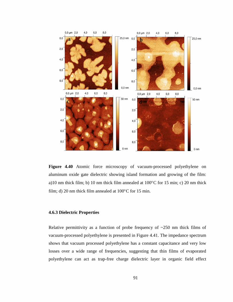
91
a b
c d
Figure 4.40 Atomic force microscopy of vacuum-processed polyethylene on
aluminum oxide gate dielectric showing island formation and growing of the film:
a)10 nm thick film; b) 10 nm thick film annealed at 100C for 15 min; c) 20 nm thick
film; d) 20 nm thick film annealed at 100C for 15 min.
4.6.3 Dielectric Properties
Relative permittivity as a function of probe frequency of ~250 nm thick films of
vacuum-processed polyethylene is presented in Figure 4.41. The impedance spectrum
shows that vacuum processed polyethylene has a constant capacitance and very low
losses over a wide range of frequencies, suggesting that thin films of evaporated
polyethylene can act as trap-free charge dielectric layer in organic field effect
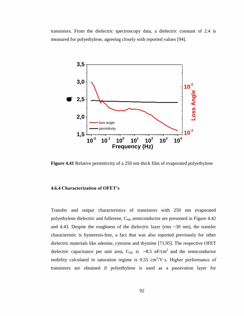
92
10-2
10-1
100
101
102
103
104
1,5
2,0
2,5
3,0
3,5
Lo
ss A
ng
le
r
Frequency (Hz)
permittivity
10-3
10-2
loss angle
transistors. From the dielectric spectroscopy data, a dielectric constant of 2.4 is
measured for polyethylene, agreeing closely with reported values [94].
Figure 4.41 Relative permittivity of a 250 nm-thick film of evaporated polyethylene
4.6.4 Characterization of OFET’s
Transfer and output characteristics of transistors with 250 nm evaporated
polyethylene dielectric and fullerene, C60, semiconductor are presented in Figure 4.42
and 4.43. Despite the roughness of the dielectric layer (rms ~30 nm), the transfer
characteristic is hysteresis-free, a fact that was also reported previously for other
dielectric materials like adenine, cytosine and thymine [71,95]. The respective OFET
dielectric capacitance per unit area, C0d, is ~8.5 nF/cm2
and the semiconductor
mobility calculated in saturation regime is 0.55 cm2/V·s. Higher performance of
transistors are obtained if polyethylene is used as a passivation layer for
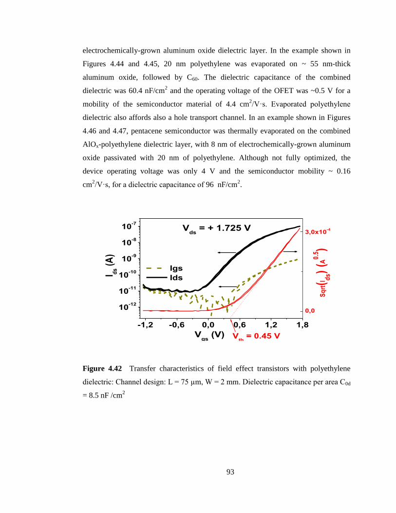
93
electrochemically-grown aluminum oxide dielectric layer. In the example shown in
Figures 4.44 and 4.45, 20 nm polyethylene was evaporated on ~ 55 nm-thick
aluminum oxide, followed by C60. The dielectric capacitance of the combined
dielectric was 60.4 nF/cm2 and the operating voltage of the OFET was ~0.5 V for a
mobility of the semiconductor material of 4.4 cm2/V·s. Evaporated polyethylene
dielectric also affords also a hole transport channel. In an example shown in Figures
4.46 and 4.47, pentacene semiconductor was thermally evaporated on the combined
AlOx-polyethylene dielectric layer, with 8 nm of electrochemically-grown aluminum
oxide passivated with 20 nm of polyethylene. Although not fully optimized, the
device operating voltage was only 4 V and the semiconductor mobility ~ 0.16
cm2/V·s, for a dielectric capacitance of 96 nF/cm
2.
-1,2 -0,6 0,0 0,6 1,2 1,8
10-12
10-11
10-10
10-9
10-8
10-7
0,0
3,0x10⁻⁴
Sq
rt(I d
s)
(A0
.5)
Igs
IdsI ds (
A)
Vgs
(V)
Vds
= + 1.725 V
Vth = 0.45 V
Figure 4.42 Transfer characteristics of field effect transistors with polyethylene
dielectric: Channel design: L = 75 µm, W = 2 mm. Dielectric capacitance per area C0d
= 8.5 nF /cm2
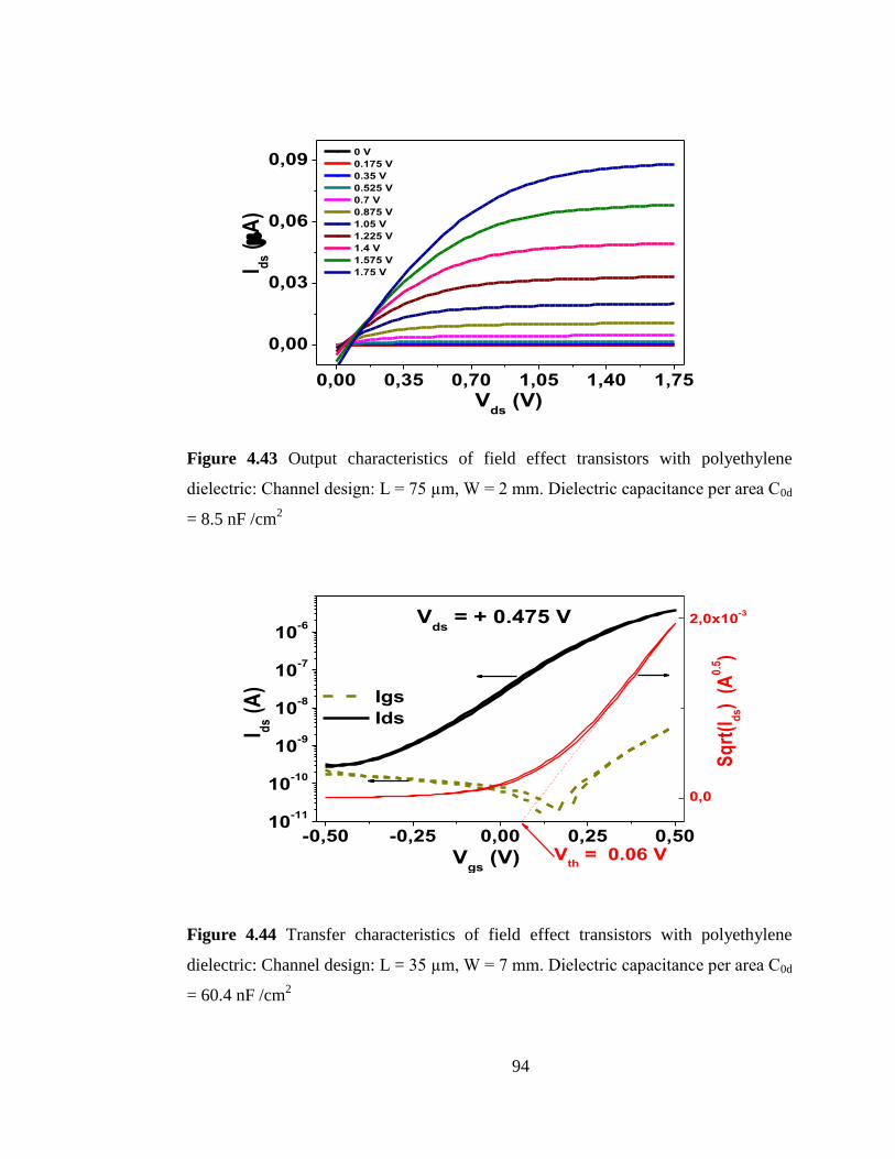
94
0,00 0,35 0,70 1,05 1,40 1,75
0,00
0,03
0,06
0,09
I ds (A
)
Vds
(V)
0 V
0.175 V
0.35 V
0.525 V
0.7 V
0.875 V
1.05 V
1.225 V
1.4 V
1.575 V
1.75 V
Figure 4.43 Output characteristics of field effect transistors with polyethylene
dielectric: Channel design: L = 75 µm, W = 2 mm. Dielectric capacitance per area C0d
= 8.5 nF /cm2
-0,50 -0,25 0,00 0,25 0,5010
-11
10-10
10-9
10-8
10-7
10-6
0,0
2,0x10⁻³
Vth
= 0.06 V
Sq
rt(I
ds)
(A
0.5)
Igs
Ids
I ds (
A)
Vgs
(V)
Vds
= + 0.475 V
Figure 4.44 Transfer characteristics of field effect transistors with polyethylene
dielectric: Channel design: L = 35 µm, W = 7 mm. Dielectric capacitance per area C0d
= 60.4 nF /cm2
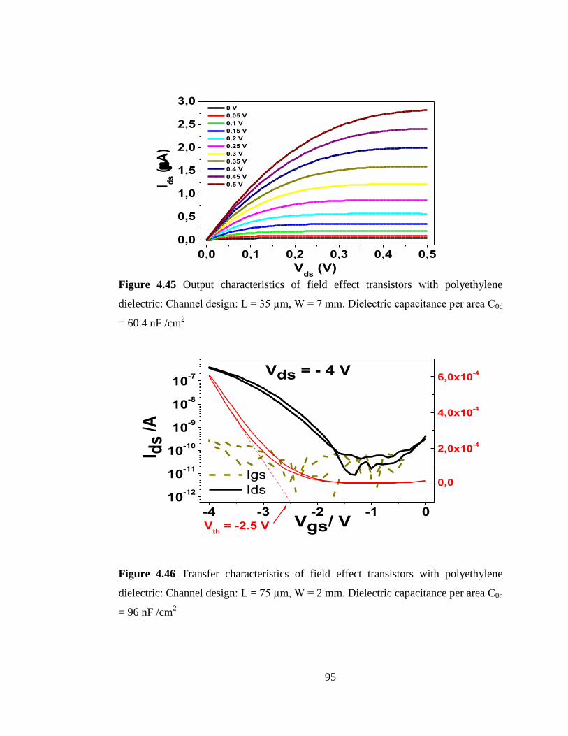
95
0,0 0,1 0,2 0,3 0,4 0,5
0,0
0,5
1,0
1,5
2,0
2,5
3,0
I ds (A
)
Vds
(V)
0 V
0.05 V
0.1 V
0.15 V
0.2 V
0.25 V
0.3 V
0.35 V
0.4 V
0.45 V
0.5 V
Figure 4.45 Output characteristics of field effect transistors with polyethylene
dielectric: Channel design: L = 35 µm, W = 7 mm. Dielectric capacitance per area C0d
= 60.4 nF /cm2
-4 -3 -2 -1 0
10-12
10-11
10-10
10-9
10-8
10-7
0,0
2,0x10⁻⁴
4,0x10⁻⁴
6,0x10⁻⁴
Vgs/ V
I ds
/A
Igs
Ids
Vds = - 4 V
Vth
= -2.5 V
Figure 4.46 Transfer characteristics of field effect transistors with polyethylene
dielectric: Channel design: L = 75 µm, W = 2 mm. Dielectric capacitance per area C0d
= 96 nF /cm2
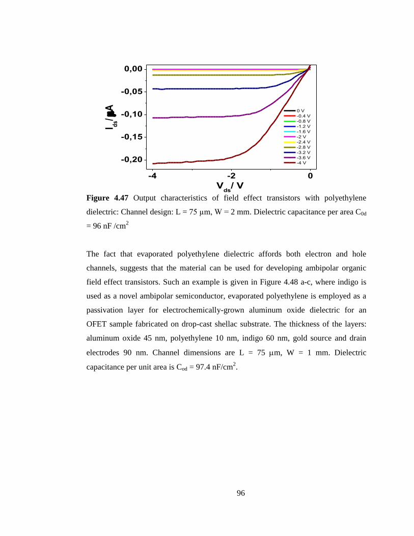
96
-4 -2 0
-0,20
-0,15
-0,10
-0,05
0,00
I ds/ A
Vds
/ V
0 V
-0.4 V
-0.8 V
-1.2 V
-1.6 V
-2 V
-2.4 V
-2.8 V
-3.2 V
-3.6 V
-4 V
Figure 4.47 Output characteristics of field effect transistors with polyethylene
dielectric: Channel design: L = 75 µm, W = 2 mm. Dielectric capacitance per area C0d
= 96 nF /cm2
The fact that evaporated polyethylene dielectric affords both electron and hole
channels, suggests that the material can be used for developing ambipolar organic
field effect transistors. Such an example is given in Figure 4.48 a-c, where indigo is
used as a novel ambipolar semiconductor, evaporated polyethylene is employed as a
passivation layer for electrochemically-grown aluminum oxide dielectric for an
OFET sample fabricated on drop-cast shellac substrate. The thickness of the layers:
aluminum oxide 45 nm, polyethylene 10 nm, indigo 60 nm, gold source and drain
electrodes 90 nm. Channel dimensions are L = 75 m, W = 1 mm. Dielectric
capacitance per unit area is Cod = 97.4 nF/cm2.
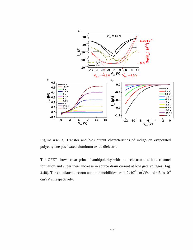
97
-12 -9 -6 -3 0 3 6 9 1210
-14
10-12
10-10
10-8
10-6
Igs
Ids
Sq
rt(I
ds)
(A
0.5)
I ds (
A)
Vds
= 12 V
0.0
6.0x10⁻⁴
Vth-h
= -4.5 VV
gs (V)
a)
Vth-e
= 4.5 V
0 3 6 9 12 15-0.1
0.0
0.1
0.2
0.3
0.4
0.5
0.6
Vds
(V)
I ds (A
)
-3 V
-1.5 V
0 V
1.5 V
3 V
4.5 V
6 V
7.5 V
9 V
10.5 V
12 V
b)
-12 -10 -8 -6 -4 -2 0
-1.2
-0.9
-0.6
-0.3
0.0
I ds (A
)
Vds
(V)
c)
4 V
2.4 V
0.8 V
-0.8 V
-2.4 V
-4 V
-5.6 V
-7.2 V
-8.8 V
-10.4 V
-12 V
Figure 4.48 a) Transfer and b-c) output characteristics of indigo on evaporated
polyethylene passivated aluminum oxide dielectric
The OFET shows clear print of ambipolarity with both electron and hole channel
formation and superlinear increase in source drain current at low gate voltages (Fig.
4.48). The calculated electron and hole mobilities are ~ 2x10⁻²
cm2/Vs and ~5.1x10
-3
cm2/V·s, respectively.
98
CHAPTER 5
CONCLUSION
5.1 Polypropylene / Carbon Black Composites
PP/CB composites were prepared via melt blending PP with CB. Effect of processing
type on mechanical and physical properties was investigated. Injection molded
samples had better mechanical properties when compared with compression molded
samples due to the orientation of the polymer chain in the direction of the applied
force. Electrical conductivity increased more in compression molded samples with
added carbon black. Percent elongation at break values of the samples decreased with
increasing filler content. The relation between percent elongation at break and
electrical conductivity was studied. After percolation threshold a sudden increase in
electrical conductivity was observed. Increasing filler content after threshold point
show negative effect on percent deformation at break. Addition of the carbon black
improved the thermal properties of the composites.
5.2 Surface Modification of Carbon Nanotube
In this study the effect of sulfonation amount of CN on electrical conductivity,
morphology and dispersion stability in water were studied. The electrical
conductivity of the CN increased with increasing sulfonation amount. SEM
micrograph of the modified samples showed that after sulfonation CN‟s were
observed in more bulky form due to strong hydrogen bonding between the CN‟s. Zeta
potential of the CN‟s increased with surface modification. The zeta potential of the
99
CN were measured as lower than -15mV. This result show that modified CN can
form stable dispersion in water.
5.3 Surface Modification of Fullerene
The effect of sulfonation degree of fullerenes on electrical conductivity, morphology
and dispersion stability in water were studied in this work. The electrical conductivity
of the fullerene increased with increasing sulfonation degree. SEM micrographs of
the material show that treatment with acid does not effect on particle size. TEM
micrographs of the samples show that after functionalization, materials have good
dispersion in water. Zeta potential of the fullerene‟s increased with surface
modification. The zeta potential of the surface modified fullerenes were found as
lower than -15mV. This result shows that modified fullerenes can form stable
dispersion in water.
5.4 Polypropylene/ Carbon Nanotube Composites
In this study, the electrical, mechanical and thermal stability of PP/neat CNT and
PP/m-CNT composites were studied. The effect of surface modification and using
different dispersants on these properties were investigated. The best electrical and
mechanical properties were observed for the composites which contain CTAB and
MA-g-PP as dispersant. CTAB had good interaction with negatively charged m-CNT
surface and as a result of this interaction both electrical and the mechanical properties
of the composites were good. Addition of MA-g-PP as dispersant increased the
Young modulus of the composites and improved the electrical conductivity.
100
5.5 Polypropylene / Fullerene Composites
Polypropylene/neat F and Polypropylene/m-F composites were prepared via melt
blending. The effect of the compatibilizer on mechanical and electrical properties of
the m-F were studied. Addition of the CTAB and MA-g-PP compatibilizer improved
the mechanical and electrical properties better than the PE-b-PEG and Triton X 100
compatibilizers. Composites which contain m-F without compatibilizer showed lower
mechanical properties than the neat fullerene composites. Mechanical properties of
the composites increased with decreasing agglomeration size.
5.6 Organic Field Effect Transistors with Polyethylene Gate Dielectric
We demonstrate that vacuum-processed polyethylene represents a good dielectric
layer for the development of high performance organic field effect transistors.
Polyethylene has excellent insulating properties, given by its high band gap of ~8.9
eV and its extremely low conductivity of ~ 110-18
S/cm. Its chemical stability is an
additional attractive feature. Vacuum-evaporated layers of polyethylene can perform
either as a stand-alone dielectric or in combination with aluminum oxide for the
attainment of efficient charge transport in OFETs. The best C60 devices built in our
lab showed operating voltages as low as 0.5 V and field effect mobilities of ~ 3.8
cm2/V·s. In addition, the possibility that both electrons and holes can be transported
at the interface polyethylene-organic semiconductor, as demonstrated by indigo,
recommends the vacuum-processed polyethylene as a suitable dielectric for the
development of ambipolar OFETs and integrated circuits.
101
REFERENCES
[1] V.E. Gul, Structure and Properties of Conducting Polymer Composites, VSP
BV, 1996.
[2] L. Chua, J. Zaumseil, J. Chang, and E.C. Ou, “General observation of n-type
field-effect behaviour in organic semiconductors,” Nature, vol. 434, 2005, pp.
194-199.
[3] Y. Ueda, M. Matsushita, S. Morimoto, J. Ping Ni, H. Suzuki, and S. Mashiko,
“Structure and crystal growth of low molecular weight polyethylene vapor-
deposited on polymer friction-transferred layers,” Thin Solid Films, vol. 331,
Oct. 1998, pp. 216-221.
[4] K. Maki, “Evaporation of polyethylene powder for its thin film growth,” Thin
Solid Films, vol. 188, Jul. 1990, pp. 355-359.
[5] R. Ebewele, Polymer Science and Technology, CRC Press, 2000.
[6] H.G. Karian, Handbook of Polypropylene and Polyropylene composites,
Marcel Dekker Inc., 2003.
[7] R. Stewart, V. Goodship, F. Guild, M. Green, and J. Farrow, “Investigation
and demonstration of the durability of air plasma pre-treatment on
polypropylene automotive bumpers,” International Journal of Adhesion and
Adhesives, vol. 25, Apr. 2005, pp. 93-99.
[8] W. Hufenbach, R. Böehm, M. Thieme, a Winkler, E. Mäder, J. Rausch, and M.
Schade, “Polypropylene/glass fibre 3D-textile reinforced composites for
102
automotive applications,” Materials & Design, vol. 32, Sep. 2010, pp. 1468-
1476.
[9] P. Tos, S. Artiaco, S. Coppolino, L.G. Conforti, and B. Battiston, “A simple
sterile polypropylene fingernail substitute.,” Chirurgie de la main, vol. 28, Jun.
2009, pp. 143-5.
[10] C. Mao, “Introduction of anticoagulation group to polypropylene film by
radiation grafting and its blood compatibility,” Applied Surface Science, vol.
228, Apr. 2004, pp. 26-33.
[11] J.-M. Thomassin, I. Huynen, R. Jerome, and C. Detrembleur, “Functionalized
polypropylenes as efficient dispersing agents for carbon nanotubes in a
polypropylene matrix; application to electromagnetic interference (EMI)
absorber materials,” Polymer, vol. 51, Jan. 2010, pp. 115-121.
[12] Y. Kanbur and Z. Kucukyavuz, “Electrical and Mechanical Properties of
Polypropylene/Carbon Black Composites,” Journal of Reinforced Plastics and
Composites, vol. 28, Oct. 2008, pp. 2251-2260.
[13] S. Bao and S. Tjong, “Mechanical behaviors of polypropylene/carbon
nanotube nanocomposites: The effects of loading rate and temperature,”
Materials Science and Engineering: A, vol. 485, Jun. 2008, pp. 508-516.
[14] J. Thomason, “The influence of fibre length and concentration on the
properties of glass fibre reinforced polypropylene: 5. Injection moulded long
and short fibre PP,” Composites Part A: Applied Science and Manufacturing,
vol. 33, Dec. 2002, pp. 1641-1652.
[15] A.M.M. Baker and J. Mead, “Thermoplastics,” Handbook of Plastics,
elastomers and composites, C.A. Harper, ed., McGraw-Hill Professional, 2004.
103
[16] R.A. Petrick, Polymer Structure Characterization (From Nano to Macro
Organization), The Royal Society of Chemistry, 2007.
[17] E.C. Carraher, Polymer Chemistry, Mercel Dekker ,Inc., 2003.
[18] J. Zaumseil and H. Sirringhaus, “Electron and ambipolar transport in organic
field-effect transistors.,” Chemical reviews, vol. 107, Apr. 2007, pp. 1296-323.
[19] J. Veres, S. Ogier, G. Lloyd, and D. de Leeuw, “Gate Insulators in Organic
Field-Effect Transistors,” Chemistry of Materials, vol. 16, Nov. 2004, pp.
4543-4555.
[20] K.J. Less and E.G. Wilson, “Intrinsic photoconduction and photoemission in
polyethylene,” Journal of Physics C: Solid State Physics, vol. 6, 1973, pp.
3110-3120.
[21] J.F. Fowler, “X-Ray Induced Conductivity in Insulating Materials,”
Proceedings of the Royal Society A: Mathematical, Physical and Engineering
Sciences, vol. 236, Sep. 1956, pp. 464-480.
[22] S. Lijima, “Helical microtubules of graphitic carbon,” Nature, vol. 354, 1991,
pp. 56-58.
[23] S.G. Shonaike, G.O. Advani, Advanced Polymeric Materials (structure and
Property Relatioship), CRC Press, 2003.
[24] M. Xanthos, Functional Fillers for Plastics, WILEY-VCH Verlag GmbH,
2005.
[25] J. Coleman, U. Khan, W. Blau, and Y. Gunko, “Small but strong: A review of
the mechanical properties of carbon nanotube–polymer composites,” Carbon,
vol. 44, Aug. 2006, pp. 1624-1652.
104
[26] Z. Spitalsky, D. Tasis, K. Papagelis, and C. Galiotis, “Carbon nanotube–
polymer composites: Chemistry, processing, mechanical and electrical
properties,” Progress in Polymer Science, vol. 35, Mar. 2010, pp. 357-401.
[27] J. Wang and Y. Lin, “Functionalized carbon nanotubes and nanofibers for
biosensing applications.,” Trends in analytical chemistry : TRAC, vol. 27, Jan.
2008, pp. 619-626.
[28] R.A. Hatton, N.P. Blanchard, L.W. Tan, G. Latini, F. Cacialli, and S.R.P.
Silva, “Oxidised carbon nanotubes as solution processable, high work function
hole-extraction layers for organic solar cells,” Organic Electronics, vol. 10,
May. 2009, pp. 388-395.
[29] P. Hernández-Fernández, M. Montiel, P. Ocón, J.L.G. de la Fuente, S. García-
Rodríguez, S. Rojas, and J.L.G. Fierro, “Functionalization of multi-walled
carbon nanotubes and application as supports for electrocatalysts in proton-
exchange membrane fuel cell,” Applied Catalysis B: Environmental, vol. 99,
Aug. 2010, pp. 343-352.
[30] X. Jiang, Y. Bin, and M. Matsuo, “Electrical and mechanical properties of
polyimide–carbon nanotubes composites fabricated by in situ polymerization,”
Polymer, vol. 46, Aug. 2005, pp. 7418-7424.
[31] R. Haggenmueller, F. Du, J.E. Fischer, and K.I. Winey, “Interfacial in situ
polymerization of single wall carbon nanotube/nylon 6,6 nanocomposites,”
Polymer, vol. 47, Mar. 2006, pp. 2381-2388.
[32] C. Teng, C. Ma, Y. Huang, S. Yuen, C. Weng, C. Chen, and S. Su, “Effect of
MWCNT content on rheological and dynamic mechanical properties of
multiwalled carbon nanotube/polypropylene composites,” Composites Part A:
Applied Science and Manufacturing, vol. 39, Dec. 2008, pp. 1869-1875.
105
[33] F. Thiébaud and J.C. Gelin, “Characterization of rheological behaviors of
polypropylene/carbon nanotubes composites and modeling their flow in a
twin-screw mixer,” Composites Science and Technology, vol. 70, Apr. 2010,
pp. 647-656.
[34] Z. Zhou, S. Wang, L. Lu, Y. Zhang, and Y. Zhang, “Functionalization of
multi-wall carbon nanotubes with silane and its reinforcement on
polypropylene composites,” Composites Science and Technology, vol. 68, Jun.
2008, pp. 1727-1733.
[35] B. Yang, J. Shi, K. Pramoda, and S. Goh, “Enhancement of the mechanical
properties of polypropylene using polypropylene-grafted multiwalled carbon
nanotubes,” Composites Science and Technology, vol. 68, Sep. 2008, pp. 2490-
2497.
[36] S. Lee, E. Cho, S. Jeon, and J. Youn, “Rheological and electrical properties of
polypropylene composites containing functionalized multi-walled carbon
nanotubes and compatibilizers,” Carbon, vol. 45, Nov. 2007, pp. 2810-2822.
[37] S. Bose, A.R. Bhattacharyya, P.V. Kodgire, and A. Misra, “Fractionated
crystallization in PA6/ABS blends: Influence of a reactive compatibilizer and
multiwall carbon nanotubes,” Polymer, vol. 48, Jan. 2007, pp. 356-362.
[38] B. Safadi, R. Andrews, and E. a Grulke, “Multiwalled carbon nanotube
polymer composites: Synthesis and characterization of thin films,” Journal of
Applied Polymer Science, vol. 84, Jun. 2002, pp. 2660-2669.
[39] L. Chen, X. Pang, M. Qu, Q. Zhang, B. Wang, B. Zhang, and Z. Yu,
“Fabrication and characterization of polycarbonate/carbon nanotubes
composites,” Composites Part A: Applied Science and Manufacturing, vol. 37,
Sep. 2006, pp. 1485-1489.
106
[40] D. Bikiaris, A. Vassiliou, K. Chrissafis, K. Paraskevopoulos, A.
Jannakoudakis, and A. Docoslis, “Effect of acid treated multi-walled carbon
nanotubes on the mechanical, permeability, thermal properties and thermo-
oxidative stability of isotactic polypropylene,” Polymer Degradation and
Stability, vol. 93, May. 2008, pp. 952-967.
[41] T. Kashiwagi, “Thermal and flammability properties of polypropylene/carbon
nanotube nanocomposites,” Polymer, vol. 45, May. 2004, pp. 4227-4239.
[42] E. Logakis, E. Pollatos, C. Pandis, V. Peoglos, I. Zuburtikudis, C.G. Delides, a
Vatalis, M. Gjoka, E. Syskakis, and K. Viras, “Structure–property relationships
in isotactic polypropylene/multi-walled carbon nanotubes nanocomposites,”
Composites Science and Technology, vol. 70, Feb. 2010, pp. 328-335.
[43] K. Prashantha, J. Soulestin, M.F. Lacrampe, P. Krawczak, G. Dupin, and M.
Claes, “Masterbatch-based multi-walled carbon nanotube filled polypropylene
nanocomposites: Assessment of rheological and mechanical properties,”
Composites Science and Technology, vol. 69, Sep. 2009, pp. 1756-1763.
[44] L. Vaisman, H.D. Wagner, and G. Marom, “The role of surfactants in
dispersion of carbon nanotubes.,” Advances in colloid and interface science,
vol. 128-130, Dec. 2006, pp. 37-46.
[45] J.I. Kroschwitz and M.H. Grant, Encyclopedia of chemical technology, John
Wiley & Sons, Inc., 1995.
[46] C. Silvestre, S. Cimmino, and E. Di Pace, “Crystallizable Polymer Blends,”
Polymeric Materials Encyclopedia, 1996.
[47] J.A. Brydson, Plastics Materials, Reed Educational andProfessional
Publishing Ltd., 1999.
[48] R.N. Rothon, Particulate Fillers for Polymers, Rapra Technology Ltd., 2002.
107
[49] P.K. Pramanik, D. Khastgir, and T.N. Saha, “Conductive nitrile rubber
composite containing carbon fillers: Studies on mechanical properties and
electrical conductivity,” Composites, vol. 23, May. 1992, pp. 183-191.
[50] D.L.D. Chung, Carbon Fiber Composites, Butterworth-Heinemann, 1994.
[51] H. Yui, G. Wu, H. Sano, M. Sumita, and K. Kino, “Morphology and electrical
conductivity of injection-molded polypropylene/carbon black composites with
addition of high-density polyethylene,” Polymer, vol. 47, May. 2006, pp.
3599-3608.
[52] Z. Ranjbar and S. Rastegar, “Morphology and electrical conductivity behavior
of electro-deposited conductive carbon black-filled epoxy dispersions near the
insulator-conductor transition point,” Colloids and Surfaces A:
Physicochemical and Engineering Aspects, vol. 290, Nov. 2006, pp. 186-193.
[53] M.L. Clingerman, J.A. King, K.H. Schulz, and J.D. Meyers, “Evaluation of
Electrical Conductivity Models for Conductive Polymer Composites,”
Polymer, 2002, pp. 1341-1356.
[54] H. Zois, L. Apekis, and M. Omastová, “Electrical properties of carbon black-
filled polymer composites,” Macromolecular Symposia, vol. 170, 2001, pp.
249-256.
[55] H.O. Pierson, Handbook of Carbon, Graphite, Diamond and Fullerenes,
Noyes Publication, 1993.
[56] F. Langa and J.F. Nierengarten, Fullerenes :Principles and Applications, The
Royal Society of Chemistry, 2007.
[57] L. Dai, J. Lu, B. Matthews, and A.W.H. Mau, “Doping of Conducting
Polymers by Sulfonated Fullerene Derivatives and Dendrimers,” The Journal
of Physical Chemistry B, vol. 102, Apr. 1998, pp. 4049-4053.
108
[58] R. Taylor and D.R.M. Walton, “The chemistry of fullerenes,” Nature, vol. 363,
Jun. 1993, pp. 685-693.
[59] H. Peng, J.W.Y. Lam, F.S.M. Leung, T.W.H. Poon, A.X. Wu, N.-T. Yu, and
B.Z. Tang, “Synthesis of Fullerene-Containing Sol-Gel Glasses,” Journal of
Sol-Gel Science and Technology, vol. 22, pp. 205-218.
[60] J.H. Bae, A.M. Shanmugharaj, W.H. Noh, W.S. Choi, and S.H. Ryu, “Surface
chemical functionalized single-walled carbon nanotube with anchored phenol
structures: Physical and chemical characterization,” Applied Surface Science,
vol. 253, Feb. 2007, pp. 4150-4155.
[61] S.K. Mazumdar, Composites Manufacturing, CRC Press, 2002.
[62] F.L. Matthews and R.D. Rawlings, Composite Materials : Engineering and
Science, Chapman & Hall, 1996.
[63] J.H. Koo, Polymer Nanocomposites, McGraw-Hill Professional, 2006.
[64] P.M. Ajayan, L.S. Schadler, and P.V. Braun, Nanocomposite Science and
Technology, WILEY-VCH Verlag GmbH, 2003.
[65] M.S. Freund and B. Deore, Self Doped Conducting Polymers, WILEY-VCH
Verlag GmbH, 2007.
[66] T.B. Singh, N. Marjanovi , P. Stadler, M. Auinger, G.J. Matt, S. Günes, N.S.
Sariciftci, R. Schwödiauer, and S. Bauer, “Fabrication and characterization of
solution-processed methanofullerene-based organic field-effect transistors,”
Journal of Applied Physics, vol. 97, 2005, p. 083714.
[67] T.B. Singh and N.S. Sariciftci, “Progress in Plastic Electronics Devices,”
Annual Review of Materials Research, vol. 36, Aug. 2006, pp. 199-230.
109
[68] R. Ponce Ortiz, A. Facchetti, and T.J. Marks, “High-k organic, inorganic, and
hybrid dielectrics for low-voltage organic field-effect transistors.,” Chemical
reviews, vol. 110, Jan. 2010, pp. 205-39.
[69] M. Irimia-Vladu, N. Marjanovic, M. Bodea, G. Hernandez-Sosa, A.M. Ramil,
R. Schwödiauer, S. Bauer, N.S. Sariciftci, and F. Nüesch, “Small-molecule
vacuum processed melamine-C60, organic field-effect transistors,” Organic
Electronics, vol. 10, May. 2009, pp. 408-415.
[70] M. Egginger, M. Irimia-Vladu, R. Schwödiauer, a Tanda, I. Frischauf, S.
Bauer, and N.S. Sariciftci, “Mobile Ionic Impurities in Poly(vinyl alcohol)
Gate Dielectric: Possible Source of the Hysteresis in Organic Field-Effect
Transistors,” Advanced Materials, vol. 20, Mar. 2008, pp. 1018-1022.
[71] M. Irimia-Vladu, P.A. Troshin, M. Reisinger, L. Shmygleva, Y. Kanbur, G.
Schwabegger, M. Bodea, R. Schwödiauer, A. Mumyatov, J.W. Fergus, V.F.
Razumov, H. Sitter, N.S. Sariciftci, and S. Bauer, “Biocompatible and
Biodegradable Materials for Organic Field-Effect Transistors,” Advanced
Functional Materials, Sep. 2010, pp. 4069-4076.
[72] M. Irimia-Vladu, N. Marjanovic, A. Vlad, A.M. Ramil, G. Hernandez-Sosa, R.
Schwoödiauer, S. Bauer, and N.S. Sariciftci, “Vacuum-Processed Polyaniline-
C 60 Organic Field Effect Transistors,” Advanced Materials, vol. 20, Oct.
2008, pp. 3887-3892.
[73] R. Yu, L. Chen, Q. Liu, J. Lin, K.-L. Tan, S.C. Ng, H.S.O. Chan, G.-Q. Xu,
and T.S.A. Hor, “Platinum Deposition on Carbon Nanotubes via Chemical
Modification,” Chemistry of Materials, vol. 10, Jan. 1998, pp. 718-722.
[74] N. Bowler and Y. Huang, “Electrical conductivity measurement of metal plates
using broadband eddy-current and four-point methods,” Measurement Science
and Technology, vol. 16, Nov. 2005, pp. 2193-2200.
110
[75] “ Four Point Probe, http://www.imagesco.com/articles/supercond/09.html last
accessed 15th April 2011.”
[76] Z.S. Petrovi , B. Martinovi , V. Divjakovi , and J. Budinski–Simendi ,
“Polypropylene–Carbon black interaction in conductive composites,” Journal
of Applied Polymer Science, vol. 49, 1993, pp. 1659-1669.
[77] J. Adler, Y. Meir, A. Aharony, A.B. Harris, and L. Klein, “Low-concentration
series in general dimension,” Journal of Statistical Physics, vol. 58, pp. 511-
538.
[78] I. Chodák, M. Omastová, and J. Pionteck, “Relation between electrical and
mechanical properties of conducting polymer composites,” Journal of Applied
Polymer Science, vol. 82, 2001, pp. 1903-1906.
[79] M. Omastova, I. Chodak, and J. Pionteck, “Electrical and mechanical
properties of conducting polymer composites,” Synthetic Metals, vol. 102, Jun.
1999, pp. 1251-1252.
[80] E. Jakab and M. Omastova, “Thermal decomposition of polyolefin/carbon
black composites,” Journal of Analytical and Applied Pyrolysis, vol. 74, Aug.
2005, pp. 204-214.
[81] K. Hinokuma and M. Ata, “Proton Conduction in Polyhydroxy
Hydrogensulfated Fullerenes,” Journal of The Electrochemical Society, vol.
150, 2003, p. A112.
[82] Z. Sun, V. Nicolosi, D. Rickard, S.D. Bergin, D. Aherne, and J.N. Coleman,
“Quantitative Evaluation of Surfactant-stabilized Single-walled Carbon
Nanotubes: Dispersion Quality and Its Correlation with Zeta Potential,” The
Journal of Physical Chemistry C, vol. 112, Jun. 2008, pp. 10692-10699.
111
[83] B. White, S. Banerjee, S. OʼBrien, N.J. Turro, and I.P. Herman, “Zeta-
Potential Measurements of Surfactant-Wrapped Individual Single-Walled
Carbon Nanotubes,” The Journal of Physical Chemistry C, vol. 111, Aug.
2007, pp. 13684-13690.
[84] X. Xie, Y. Mai, and X. Zhou, “Dispersion and alignment of carbon nanotubes
in polymer matrix: A review,” Materials Science and Engineering: R: Reports,
vol. 49, May. 2005, pp. 89-112.
[85] L.Y. Chiang, L.-Y. Wang, J.W. Swirczewski, S. Soled, and S. Cameron,
“Efficient Synthesis of Polyhydroxylated Fullerene Derivatives via Hydrolysis
of Polycyclosulfated Precursors,” The Journal of Organic Chemistry, vol. 59,
Jul. 1994, pp. 3960-3968.
[86] H. Hu, A. Yu, E. Kim, B. Zhao, M.E. Itkis, E. Bekyarova, and R.C. Haddon,
“Influence of the Zeta Potential on the Dispersability and Purification of
Single-Walled Carbon Nanotubes,” The Journal of Physical Chemistry B, vol.
109, May. 2005, pp. 11520-11524.
[87] Q. Wang, Y. Han, Y. Wang, Y. Qin, and Z.-X. Guo, “Effect of Surfactant
Structure on the Stability of Carbon Nanotubes in Aqueous Solution,” The
Journal of Physical Chemistry B, vol. 112, May. 2008, pp. 7227-7233.
[88] A. Montazeri, J. Javadpour, A. Khavandi, A. Tcharkhtchi, and A. Mohajeri,
“Mechanical properties of multi-walled carbon nanotube/epoxy composites,”
Materials & Design, vol. 31, Oct. 2010, pp. 4202-4208.
[89] M. Yeh, N. Tai, and J. Liu, “Mechanical behavior of phenolic-based
composites reinforced with multi-walled carbon nanotubes,” Carbon, vol. 44,
Jan. 2006, pp. 1-9.
112
[90] B.B. Marosfői, a Szabó, G. Marosi, D. Tabuani, G. Camino, and S. Pagliari,
“Thermal and spectroscopic characterization of polypropylene-carbon
nanotube composites,” Journal of Thermal Analysis and Calorimetry, vol. 86,
Oct. 2006, pp. 669-673.
[91] M. Angelopoulos, G.E. Asturias, S.P. Ermer, A. Ray, E.M. Scherr, A.G.
Macdiarmid, M. Akhtar, Z. Kiss, and A.J. Epstein, “Polyaniline: Solutions,
Films and Oxidation State,” Molecular Crystals and Liquid Crystals
Incorporating Nonlinear Optics, vol. 160, 1988, pp. 151-163.
[92] J.V. Gulmine, P.R. Janissek, H.M. Heise, and L. Akcelrud, “Polyethylene
characterization by FTIR,” Polymer Testing, vol. 21, 2002, pp. 557-563.
[93] M. Mirzataheri and J. Morshedian, “Electron beam performance in the novel
solventless LDPE-NVP surface grafting system,” Radiation Physics and
Chemistry, vol. 75, Feb. 2006, pp. 236-242.
[94] M. Zor and C. a Hogarth, “High-field electrical conduction in thin films of
polyethylene,” Physica Status Solidi (a), vol. 99, Feb. 1987, pp. 513-519.
[95] M. Irimia-Vladu, P.A. Troshin, M. Reisinger, G. Schwabegger, M. Ullah, R.
Schwoediauer, A. Mumyatov, M. Bodea, J.W. Fergus, V.F. Razumov, H.
Sitter, S. Bauer, and N.S. Sariciftci, “Environmentally sustainable organic field
effect transistors,” Organic Electronics, vol. 11, Dec. 2010, pp. 1974-1990.
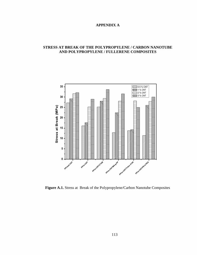
113
APPENDIX A
STRESS AT BREAK OF THE POLYPROPYLENE / CARBON NANOTUBE
AND POLYPROPYLENE / FULLERENE COMPOSITES
PP/nea
t CNT
PP/m-C
NT
PP/m-C
NT/C
TAB
PP/m-C
NT/M
A-g
-PP
PP/m-C
NT/T
riton X
100
PP/m-C
NT/P
E-b-P
EG
0
5
10
15
20
25
30
35
Str
es
s a
t B
rea
k (
MP
a)
0.5 % CNT
1 % CNT
2 % CNT
3 % CNT
Figure A.1. Stress at Break of the Polypropylene/Carbon Nanotube Composites
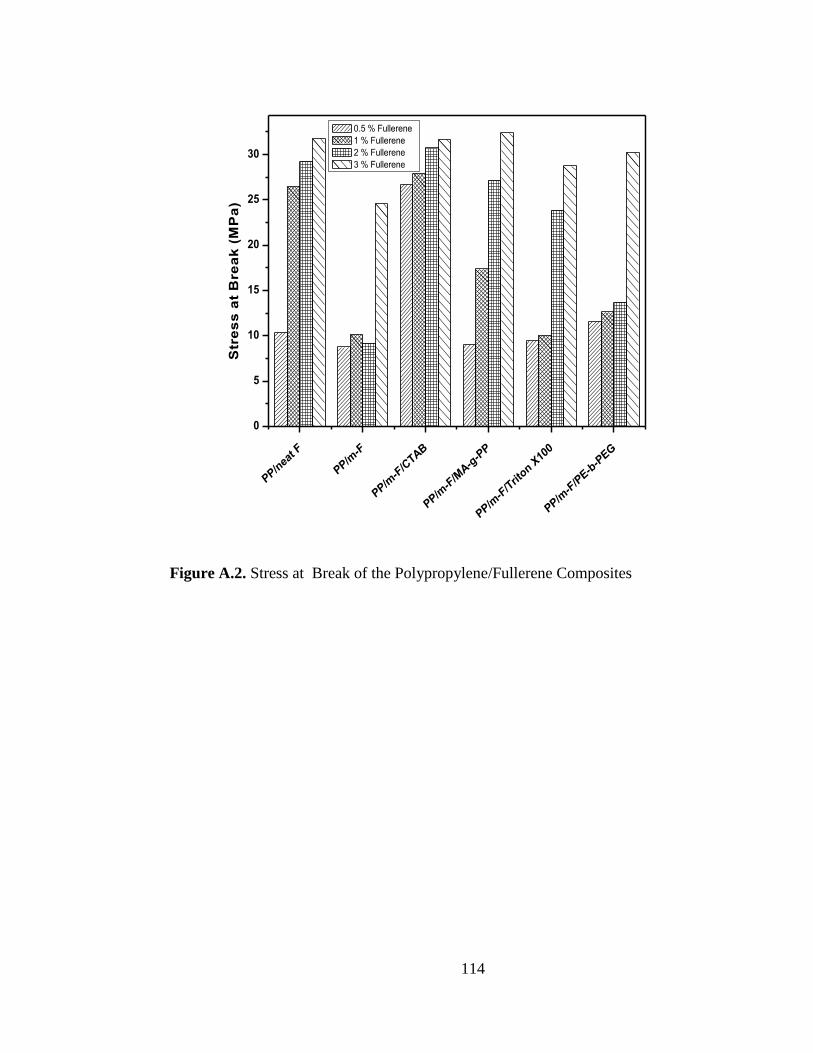
114
PP/nea
t F
PP/m-F
PP/m-F
/CTAB
PP/m-F
/MA-g
-PP
PP/m-F
/Trit
on X10
0
PP/m-F
/PE-b
-PEG
0
5
10
15
20
25
30
Str
es
s a
t B
rea
k (
MP
a)
X Axis Title
0.5 % Fullerene
1 % Fullerene
2 % Fullerene
3 % Fullerene
Figure A.2. Stress at Break of the Polypropylene/Fullerene Composites
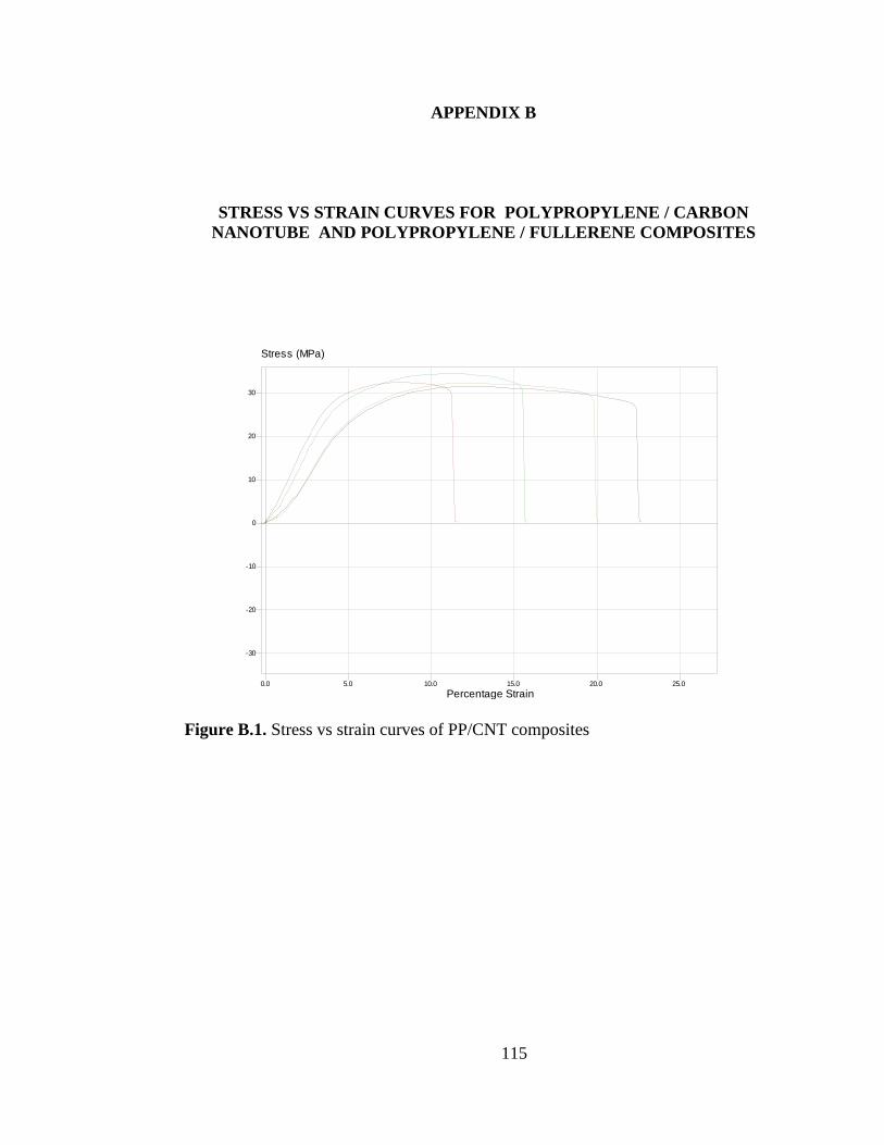
115
APPENDIX B
STRESS VS STRAIN CURVES FOR POLYPROPYLENE / CARBON
NANOTUBE AND POLYPROPYLENE / FULLERENE COMPOSITES
Stress (MPa)
-30
-20
-10
0
10
20
30
Percentage Strain0.0 5.0 10.0 15.0 20.0 25.0
Tensile Setup
5.00 cm
7.60 mm
2.00 mm
0,5 CTAB 1
Figure B.1. Stress vs strain curves of PP/CNT composites
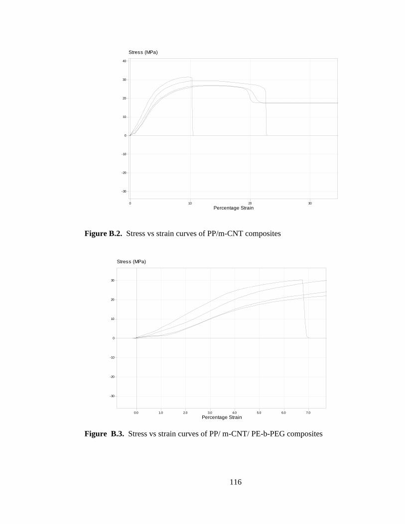
116
Stress (MPa)
-30
-20
-10
0
10
20
30
40
Percentage Strain0 10 20 30
Tensile Setup
5.00 cm
7.60 mm
2.00 mm
Figure B.2. Stress vs strain curves of PP/m-CNT composites
Stress (MPa)
-30
-20
-10
0
10
20
30
Percentage Strain0.0 1.0 2.0 3.0 4.0 5.0 6.0 7.0
Tensile Setup
5.00 cm
7.60 mm
2.00 mm
Figure B.3. Stress vs strain curves of PP/ m-CNT/ PE-b-PEG composites
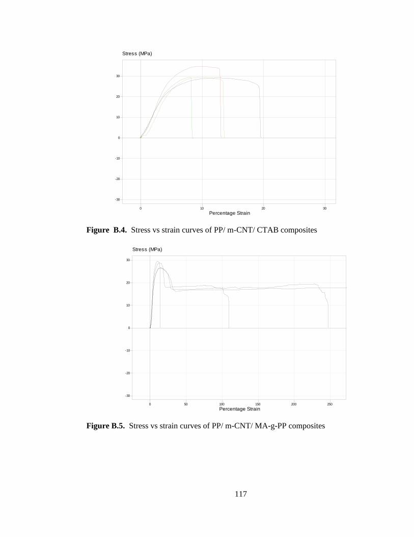
117
Stress (MPa)
-30
-20
-10
0
10
20
30
Percentage Strain0 10 20 30
Tensile Setup
5.00 cm
7.60 mm
2.00 mm
Figure B.4. Stress vs strain curves of PP/ m-CNT/ CTAB composites
Stress (MPa)
-30
-20
-10
0
10
20
30
Percentage Strain0 50 100 150 200 250
Tensile Setup
5.00 cm
7.60 mm
2.00 mm
0,5 CNT MA
Figure B.5. Stress vs strain curves of PP/ m-CNT/ MA-g-PP composites
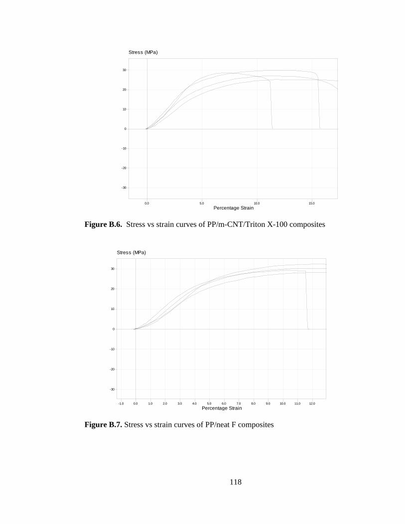
118
Stress (MPa)
-30
-20
-10
0
10
20
30
Percentage Strain0.0 5.0 10.0 15.0
Tensile Setup
5.00 cm
7.60 mm
2.00 mm
Figure B.6. Stress vs strain curves of PP/m-CNT/Triton X-100 composites
Stress (MPa)
-30
-20
-10
0
10
20
30
Percentage Strain-1.0 0.0 1.0 2.0 3.0 4.0 5.0 6.0 7.0 8.0 9.0 10.0 11.0 12.0
Tensile Setup
5.00 cm
7.60 mm
2.00 mm
Figure B.7. Stress vs strain curves of PP/neat F composites
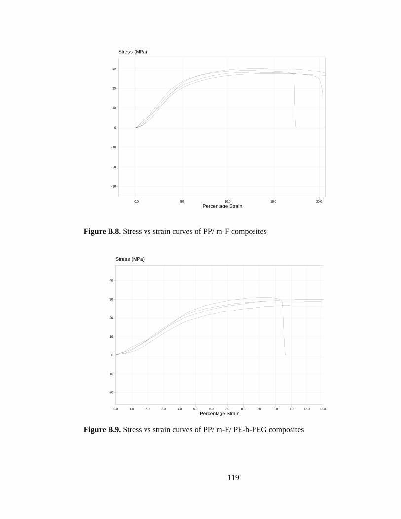
119
Stress (MPa)
-30
-20
-10
0
10
20
30
Percentage Strain0.0 5.0 10.0 15.0 20.0
Tensile Setup
5.00 cm
7.60 mm
2.00 mm
8
Figure B.8. Stress vs strain curves of PP/ m-F composites
Stress (MPa)
-20
-10
0
10
20
30
40
Percentage Strain0.0 1.0 2.0 3.0 4.0 5.0 6.0 7.0 8.0 9.0 10.0 11.0 12.0 13.0
Tensile Setup
5.00 cm
7.60 mm
2.00 mm
Figure B.9. Stress vs strain curves of PP/ m-F/ PE-b-PEG composites
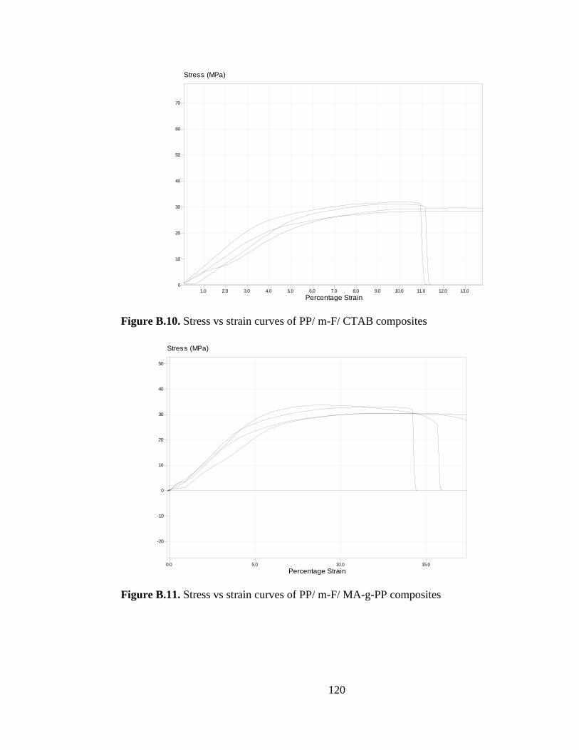
120
Stress (MPa)
0
10
20
30
40
50
60
70
Percentage Strain1.0 2.0 3.0 4.0 5.0 6.0 7.0 8.0 9.0 10.0 11.0 12.0 13.0
Tensile Setup
5.00 cm
7.60 mm
2.00 mm
7
Figure B.10. Stress vs strain curves of PP/ m-F/ CTAB composites
Stress (MPa)
-20
-10
0
10
20
30
40
50
Percentage Strain0.0 5.0 10.0 15.0
Tensile Setup
5.00 cm
7.60 mm
2.00 mm
Figure B.11. Stress vs strain curves of PP/ m-F/ MA-g-PP composites
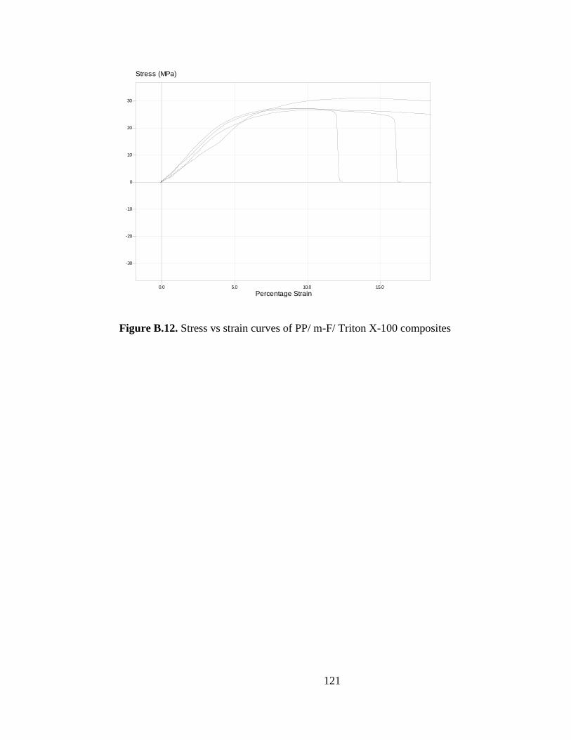
121
Stress (MPa)
-30
-20
-10
0
10
20
30
Percentage Strain0.0 5.0 10.0 15.0
Tensile Setup
5.00 cm
7.60 mm
2.00 mm
Figure B.12. Stress vs strain curves of PP/ m-F/ Triton X-100 composites
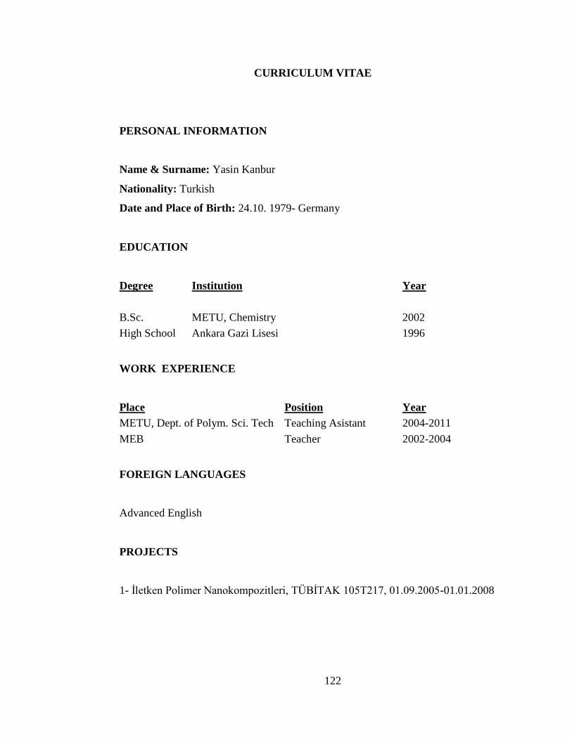
122
CURRICULUM VITAE
PERSONAL INFORMATION
Name & Surname: Yasin Kanbur
Nationality: Turkish
Date and Place of Birth: 24.10. 1979- Germany
EDUCATION
Degree Institution Year
B.Sc. METU, Chemistry 2002
High School Ankara Gazi Lisesi 1996
WORK EXPERIENCE
Place Position Year
METU, Dept. of Polym. Sci. Tech Teaching Asistant 2004-2011
MEB Teacher 2002-2004
FOREIGN LANGUAGES
Advanced English
PROJECTS
1- İletken Polimer Nanokompozitleri, TÜBİTAK 105T217, 01.09.2005-01.01.2008
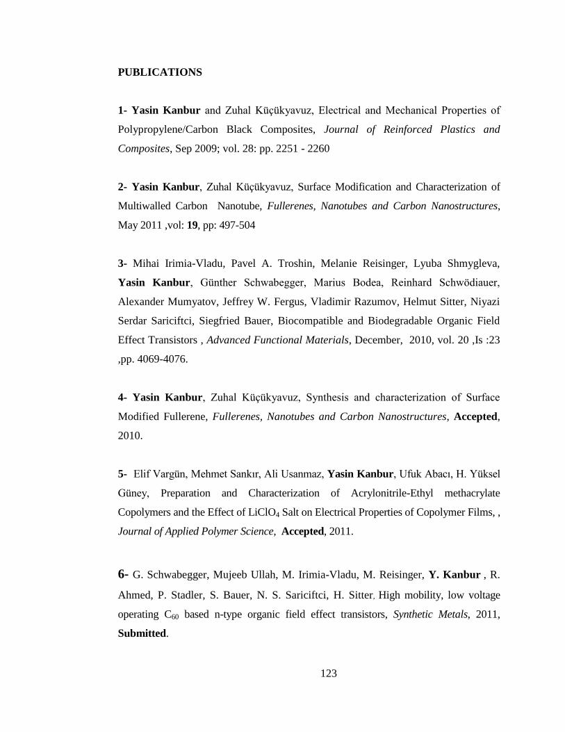
123
PUBLICATIONS
1- Yasin Kanbur and Zuhal Küçükyavuz, Electrical and Mechanical Properties of
Polypropylene/Carbon Black Composites, Journal of Reinforced Plastics and
Composites, Sep 2009; vol. 28: pp. 2251 - 2260
2- Yasin Kanbur, Zuhal Küçükyavuz, Surface Modification and Characterization of
Multiwalled Carbon Nanotube, Fullerenes, Nanotubes and Carbon Nanostructures,
May 2011 ,vol: 19, pp: 497-504
3- Mihai Irimia-Vladu, Pavel A. Troshin, Melanie Reisinger, Lyuba Shmygleva,
Yasin Kanbur, Günther Schwabegger, Marius Bodea, Reinhard Schwödiauer,
Alexander Mumyatov, Jeffrey W. Fergus, Vladimir Razumov, Helmut Sitter, Niyazi
Serdar Sariciftci, Siegfried Bauer, Biocompatible and Biodegradable Organic Field
Effect Transistors , Advanced Functional Materials, December, 2010, vol. 20 ,Is :23
,pp. 4069-4076.
4- Yasin Kanbur, Zuhal Küçükyavuz, Synthesis and characterization of Surface
Modified Fullerene, Fullerenes, Nanotubes and Carbon Nanostructures, Accepted,
2010.
5- Elif Vargün, Mehmet Sankır, Ali Usanmaz, Yasin Kanbur, Ufuk Abacı, H. Yüksel
Güney, Preparation and Characterization of Acrylonitrile-Ethyl methacrylate
Copolymers and the Effect of LiClO4 Salt on Electrical Properties of Copolymer Films, ,
Journal of Applied Polymer Science, Accepted, 2011.
6- G. Schwabegger, Mujeeb Ullah, M. Irimia-Vladu, M. Reisinger, Y. Kanbur , R.
Ahmed, P. Stadler, S. Bauer, N. S. Sariciftci, H. Sitter, High mobility, low voltage
operating C60 based n-type organic field effect transistors, Synthetic Metals, 2011,
Submitted.
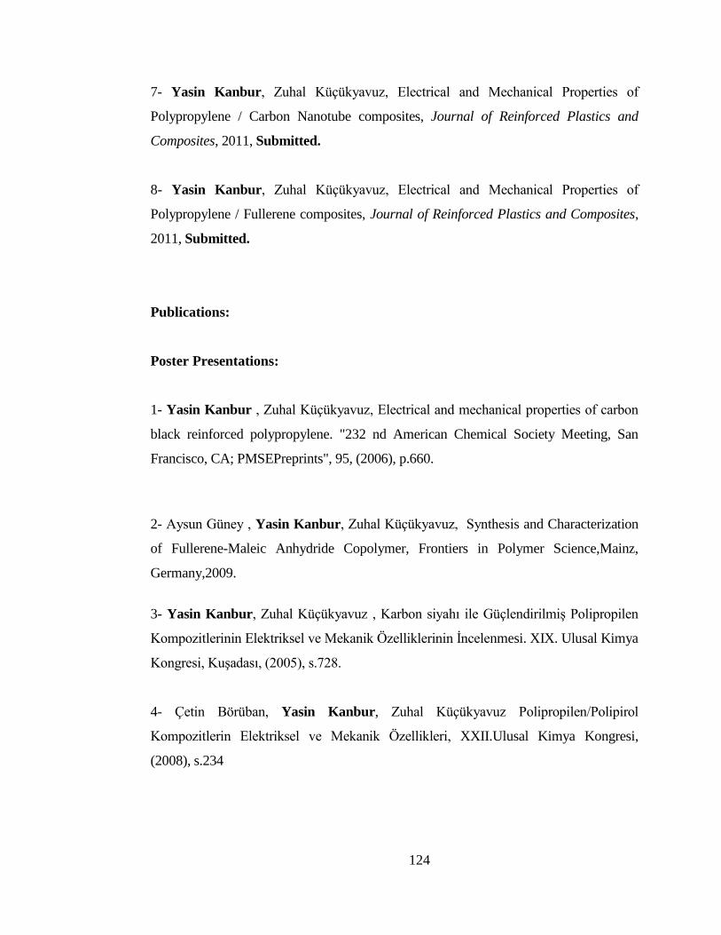
124
7- Yasin Kanbur, Zuhal Küçükyavuz, Electrical and Mechanical Properties of
Polypropylene / Carbon Nanotube composites, Journal of Reinforced Plastics and
Composites, 2011, Submitted.
8- Yasin Kanbur, Zuhal Küçükyavuz, Electrical and Mechanical Properties of
Polypropylene / Fullerene composites, Journal of Reinforced Plastics and Composites,
2011, Submitted.
Publications:
Poster Presentations:
1- Yasin Kanbur , Zuhal Küçükyavuz, Electrical and mechanical properties of carbon
black reinforced polypropylene. "232 nd American Chemical Society Meeting, San
Francisco, CA; PMSEPreprints", 95, (2006), p.660.
2- Aysun Güney , Yasin Kanbur, Zuhal Küçükyavuz, Synthesis and Characterization
of Fullerene-Maleic Anhydride Copolymer, Frontiers in Polymer Science,Mainz,
Germany,2009.
3- Yasin Kanbur, Zuhal Küçükyavuz , Karbon siyahı ile Güçlendirilmiş Polipropilen
Kompozitlerinin Elektriksel ve Mekanik Özelliklerinin İncelenmesi. XIX. Ulusal Kimya
Kongresi, Kuşadası, (2005), s.728.
4- Çetin Börüban, Yasin Kanbur, Zuhal Küçükyavuz Polipropilen/Polipirol
Kompozitlerin Elektriksel ve Mekanik Özellikleri, XXII.Ulusal Kimya Kongresi,
(2008), s.234


![Kâr ve eglence için filtreleri˘ çengellemek: PFIL HOOKSpfil_run_hooks [9] (pfil_head yapı tipinin type struct) inet_pfil_hook kuyruk sırasında girisi¸ çapraz geçer (traverses)](https://img.pdfslide.net/doc/110x75/5e53be9a471d22663c156594/kr-ve-eglence-iin-iltreleri-engellemek-pfil-pilrunhooks-9-pilhead.jpg)