Embed Size (px)
Citation preview
CROATICA CHEMICA ACTA CCACAA69 (3) 1053-1067 (1996)
ISSN-001l-1643CCA-2362 Original Scientific Paper
Contributions of Crystallographyto Materials Science*
Hartmut Fuess
Fachgebiet Strukturforschung, Fachbereich Materialwissenschaft, TechnischeHochschule Darmstadt, Petersenstra(Je 23, 64287 Darmstadt, Germany
Received March 26, 1996; revised June 24, 1996; accepted July 10, 1996
The properties of materials used in various domains of science and en-gineering are directly correlated to the microstructure. Crystal-lography is devoted to the investigaton of microstructure of substancesand materials by a variety of diffraction and spectroscopic methods.Several examples related to research in the department of materi-als science at the Technical University of Darmstadt are presented.The structure and dynamics of aromatic host molecules in catalyti-cally active zeolites are investigated by X-ray and neutron diffractionand NMR-spectroscopy combined with inelastic neutron scattering.Surfaces and interfaces of semiconductors and thin superconductingfilms are studied by grazing incidence techniques. By examination ofthe reflectogram details on thickness, composition, surface roughnessand a possible modification of these values are obtained.Transmission electron microscopy provides complementary informa-tion on the structure of interfaces, especially through the support ofsimulated images by a multi-slice method. Work is presented onCoSi2-films on Si and wafers of GaAs with LaB6 films. Modificationof the se wafers by ion mixing techniques is attempted. Furthermore,surface hardening of steel by ion implantation (carbon and nitrogen)is away of improving tribological properties. Grazing incidence pro-vides resuIts on the formation of different carbides as a function ofdepth. Superconducting films of Bi2Sr2CaCu20s on SrTi03 showed animprovement by a factor of 10 in critical current density by creatingholes (Xe,Au, U'-irradiation) as pinning centres. The examination byTEM revealed an amorphization of the channel s with dear bounda-ries between the channel and nonirradiated material.
00'Based upon the lecture presented at the Fourth Croatian-Slovenian Crystallographic Meeting,Trakošćan, Croatia, Sept 28 - Sept 30, 19950
1054 H. FUESS
INTRODUCTION
The development of »new materials- constitutes an important challengein various fields of science and engineering. Whereas the preparative chem-ist invents new substances, the engineer on the other end of the scale wantsa well characterized material with known structure and properties.
Crystallography has invented a wide range of techniques which are in-strumental in the procedure from a chemical substance into a material.Many of these techniques are based on X-ray diffraction but electron micros-copy, neutron scattering or spectroscopic methods have made important con-tributions. It is not the intention of the present paper to give a comprehen-sive review of all these fields. We shall present same examples that arerelated to the present research work of our laboratory. Additional informa-tian on the application of X-ray crystallography in chemistry is given in avolume devated to the celebration of the detection of X-rays in 1895 byRontgen.!
We shalI report here mainly on X-ray techniques devated to the charac-terizatian of surfaces and interfaces and describe the complementary use ofelectron microscopy in this field. We shalI add a chapter on the magneticproperties of superconducting material and a brief summary of our resultson host-guest interactions in micro- und mesoparaus zeolites.
HOST-GUEST INTERACTION IN ZEOLITES
Whereas the channels and voids of natural zeolites are filled with cat-ions and water molecules, catalytically active material s are produced byeither ion exchange of natural species or by direct synthesis.
A great variety of ions ar organic molecules may be introduced into thecavities and thus materials for different applications are produced. The de-compositian of Pt(NH3)42+ in zeolite NaX yields nanocrystalline platinumclusters applicable in catalysis."
Adsorption of dye molecules produces pigments.šPolar aromatic molecules like nitroaniline are of potential use for non"
linear optics (NLO). As demonstrated by Cara et .a.: the alignment of thesemolecules in the channel s of zeolites is feasible and produces a NLO-effect.Amore detailed review of zeolitic material s has been given by Kaučič in thisjournal.P
The framework of zeolites consists of T04-tetrahedra, where T = Si, Alin natural species. The tetrahedra are connected by common oxygen atoms.The charge balance is achieved by cations like Na, Ca, Ba, K in the voids.The technical application requires introduction of organic molecules into theholes.
CONTRIBUTIONS OF CRYSTALLOGRAPHY TO MATERIALS SCIENCE 1055
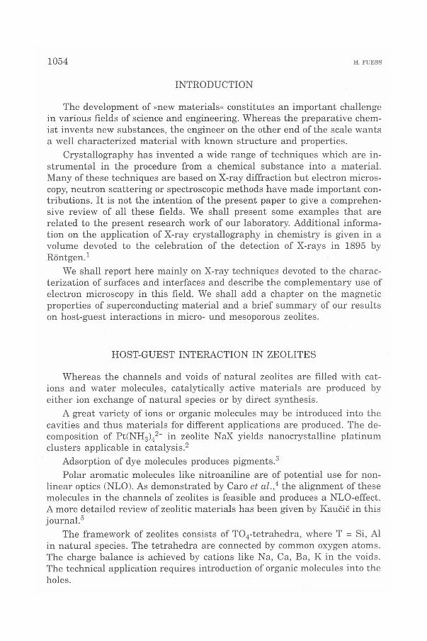
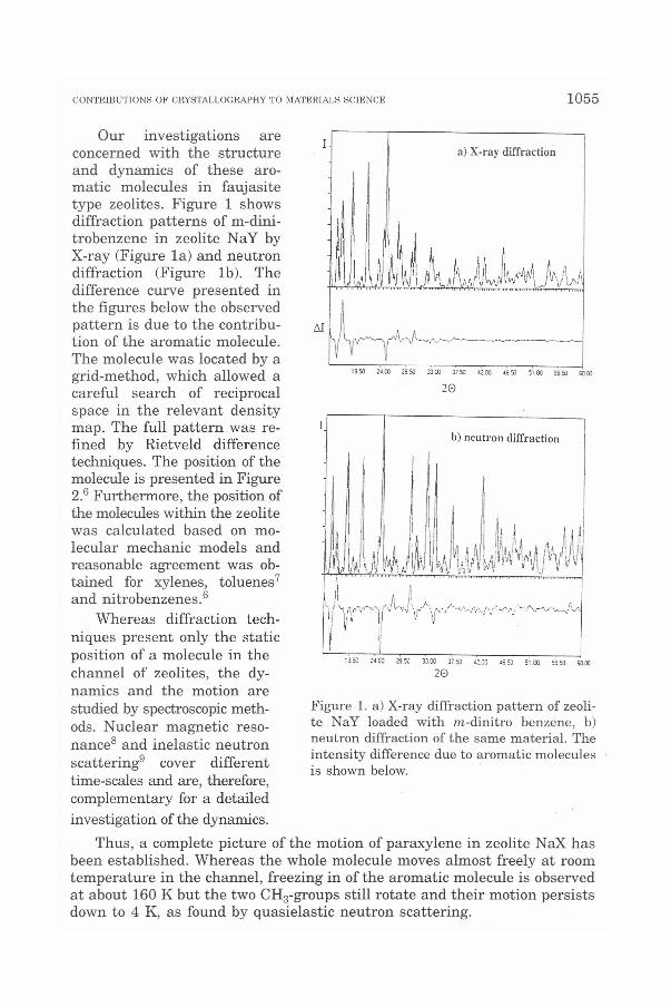
Our investigations areconcerned with the structureand dynamics of these aro-matic molecules in faujasitetype zeolites. Figure 1 showsdiffraction patterns of m-dini-trobenzene in zeolite NaY byX-ray (Figure la) and neutrondiffraction (Figure 1b). Thedifference curve presented inthe figure s below the observedpattern is due to the contribu-tion of the aromatic molecule.The molecule was located by agrid-method, which alIowed acareful search of reciprocalspace in the relevant densitymap. The full pattern was re-fined by Rietveld differencetechniques. The position of themolecule is presented in Figure2.6 Furthermore, the position ofthe moleculeswithin the zeolitewas calculated based on mo-lecular mechanic models andreasonable agreement was ob-tained for xylenes, toluenes 7and nitrobenzenes."
Whereas diffraction tech-niques present only the staticposition of a molecule in thechannel of zeolites, the dy-namics and the motion arestudied by spectroscopicmeth-ods. Nuclear magnetic reso-nance" and inelastic neutronscattering? cover differenttime-scales and are, therefore,complementary for a detailedinvestigation of the dynamics.
Thus, a complete picture of the motion of paraxylene in zeolite NaX hasbeen established. Whereas the whole molecule moves almost freely at roomtemperature in the channel, freezing in of the aromatic molecule is observedat about 160 K but the two CH3-groups still rotate and their motion persistsdown to 4 K, as found by quasielastic neutron scattering.
a) Xvray diffraction
i ~ A ~ AAjJJf~tfrA~~~-r4-c-~---~-~-,-
,19_50 2' 00 28.50 3300 J1 so 42.00 '1:150 5100 55.50 60_00
20
Ib) neutron diffraction
I,
I 11)1 II
I ,I I I 1111 Jtl d \11,it ~h.l)~~~~.j~\Jj "'~ VltV l'.Ail~~~V~/Vlj'i\j\J I'il . ',,' . ....1\ ' li
"II (rv: -r'>.....,"1·';\('··,-·;,;,·· ..h'-V"'~.J\/'.
~ I., 3:100 )7:oJ ~2.00 Jlj:u SLOCI 55.50 60.00
20
Figure 1. a) X-ray diffraction pattern of zeoli-te NaY loaded with m-dinitro benzene, b)neutron diffraction of the same material. Theintensity difference due to aromatic moleculesis shown below.
1056 H. FUESS
1 molecule / sc
1 molecule / sc+
water
Figure 2. Arrangement of m-dinitrobenzene in the supercage of faujasite NaY, dif-ferent loadings and water content.
SURFACE X-RAY DIFFRACTION
The characterization of surfaces and interfaces is a prerequisite for thepreparation of a variety of materials, especiaUy for semiconductors but alsofor the whole class of nanostructured materials. Whereas X-ray techniquesare non-destructive, the preparation techniques for transmission electronmicroscopy (TEM) studies need preparation techniques that may modify thespecimen.
Reflectometry
Investigation of the surfaces of materials by X-ray diffraction is deter-mined by absorption and reflectivity of this radiation. The method is based
"
CONTRIBUTIONS OF CRYSTALLOGRAPHY TO MATERIALS SCIENCE 1057
on the index of refraction of the material und er study and of the differencesin this index hetween materials.
n = 1 - 5 + ifJ
where 5 is proportional to the the real part (f) and fJ proportional to theimaginary part (f') of the atomic form factor (f = t; + f + ir). The numericalvalue of the refractive index is slight1y smaller than unity, e.g. for Fe andCuKa - radiation n = 0.9975. Any material is therefore less dense than airfor the scattering of X-rays from surfaces hence total reflection occurs forsmall angles of incidence. The critical angle for total reflection is given as
G - >12&c -
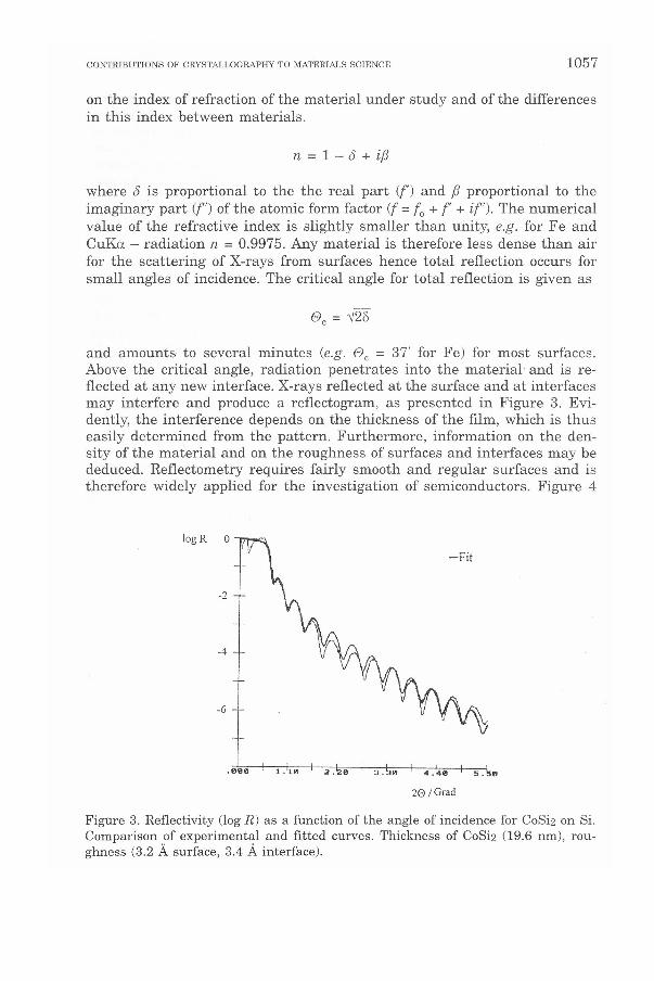
and amounts to several minutes (e.g. ec = 37' for Fe) for most surfaces.Ahove the critical angle, radiation penetrates into the material and is re-flected at any new interface. X-rays reflected at the surface and at interfacesmay interfere and produce a reflectogram, as presented in Figure 3. Evi-dently, the interference depends on the thickness of the film, which is thuseasily determined from the pattern. Furthermore, information on the den-sity of the material and on the roughness of surfaces and interfaces may hededuced. Reflectometry requires fairly smooth and regular surfaces and istherefore widely applied for the investigation of semiconductors. Figure 4
logR o
-2
-4
5. I'
-6
.1' I!! 1. J.I!!
20/Grad
Figure 3. Reflectivity (log R) as a function of the angle of incidence for COSi2on Si.Comparison of experimental and fitted curves. Thickness of COSi2(19.6 nm), rou-ghness (3.2 Asurface, 3.4 A interface).
1058
.1."e.-- __ ~
~! -1.48~·"q.)
'~AI
. "" . J.. e e .1.:58 a .'88 ...
:~ -2.68
-3.08
.....1.CD,----~
.eeeh~, b)~-;-;~ -1. e e
~
~·~:.., -4:. "eFrt
-:J.ee
~..... •5!l~ .l,'IHI 1. • 2 .• 2.58
-~• -1. ee
.5'88
c)
..·"~j -2. e e
>, . !ltle -t---- .
-3.ee
l.'ee2 Thet .• .I C,...•d
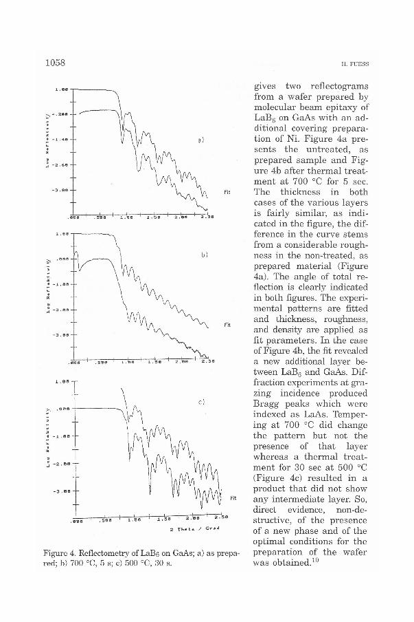
Figure 4. Refleetometry of LaB6 on GaAs; a) as prepa-red; b) 700 °C, 5 s; c) 500 °C, 30 s.
H. FUESS
gives two reflectogramsfrom a wafer prepared bymolecular beam epitaxy ofLaB6 on GaAs with an ad-ditional covering prepara-tion of Ni. Figure 4a pre-sents the untreated, asprepared sample and Fig-ure 4b after thermal treat-ment at 700 °C for 5 sec.The thickness in bothcases of the various layersis fairly similar, as indi-cated in the figure, the dif-ference in the curve stemsfrom a considerable rough-ness in the non-treated, asprepared material (Figure4a). The angle of total re-flection is clearly indicatedin both figures. The experi-mental patterns are fittedand thickness, roughness,and density are applied asfit parameters. In the caseofFigure 4b, the fit revealeda new additional layer be-tween LaB6and GaAs. Dif-fraction experiments at gra-zing incidence producedBragg peaks which wereindexed as LaAs. Temper-ing at 700 °C did changethe pattern but not thepresence of that layerwhereas a thermal treat-ment for 30 sec at 500 °C(Figure 4c) resulted in aproduct that did not showany intermediate layer. So,direct evidence, non-de-structive, of the presenceof a new phase and of theoptimal conditions for thepreparation of the waferwas obtained'?
CONTRIBUTIONS OF CRYSTALLOGRAPHY TO MATERIALS SCIENCE 1059
Grazing incidenee diffraction
Due to absorption, the penetration of X-rays in material is limited butstill amounts to several um for Cu Ka radiation. It is therefore not normallysuited for an investigation of surface effects. But at low incidence angles,the dependence of the penetration length p may be varied as a function ofthe incidence angle a
p "" sin a/I-')5
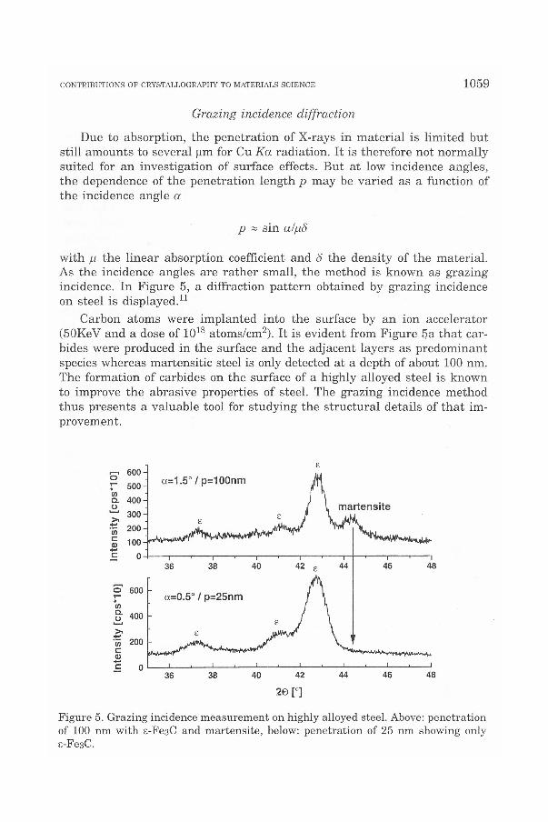
with f.1 the linear absorption coefficient and 8 the density of the material.As the incidence angles are rather small, the method is known as grazingincidence. In Figure 5, a diffraction pattern obtained by grazing incidenceon steel is displayed.P
Carbon atoms were implanted into the surface by an ion accelerator(50KeV and a dose of 1018 atoms/cm''). It is evident from Figure 5a that car-bides were produced in the surface and the adjacent layers as predominantspecies whereas martensitic steel is only detected at a depth of about 100 nm.The formation of carbides on the surface of a highly alloyed steel is knownto improve the abrasive properties of steel. The grazing incidence methodthus presents a valuable tool for studying the structural details of that im-provement.
E
5' 600,.... 500 a=1.5° I p=1 OOnm.ulcl. 400~ 300>-•.. 200'iiic: 100<li"E o
36 38 40 42 E 44 46 48
5' 600a=O.5° I p=25nm,.....ulcl. 400~
>-:!:: 200ulc:<li•....:: o 36 38 40 42 44 46 48
20 nFigure 5. Grazing incidenee measurement on highly alloyed ste el. Above: penetrationof 100 nm with E-Fe3Cand martensite, below: penetration of 25 nm showing onlyE-Fe3C.
1060 H. FUESS
Real structure of thin films
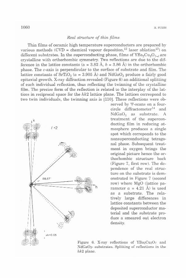
Thin films of ceramic high temperature superconductors are prepared byvarious methods (CVD = chemical vapour deposition.F laser ablation+') ondifferent substrates. In the superconducting phase, films ofYBa2Cu307....8 arecrystalline with orthorhombic symmetry. Two reflections are due to the dif-ference in the lattice constants (a = 3.82 A., b = 3.86 A.) in the orthorhombicphase. The c-axis is perpendicular to the surface of substrate and film. Thelattice constants of SrTi03 (a = 3.905 A.) and NdGa03 produce a fairly goodepitaxial growth. X-ray diffraction revealed (Figure 6) an additional splittingof each individual reflection, thus reflecting the twinning of the crystallinefilm. The precise form of the reflection is related to the interplay of the lat-tices in reciprocal space for the hk2 lattice plane. The lattices correspond totwo twin individuals, the twinning axis is [110]. These reflections were ob-
served by q'-scans on a four-circle diffractometer+" andNdGa03 as substrate. Atreatment of the supercon-ducting film in reducing at-mosphere produces asinglespot which correponds to thenonsuperconducting tetrago-nal phase. Subsequent treat-ment in oxygen brings theoriginal picture hence the 01'-
thorhombic structure back(Figure 7, first row). The de-pendence of the real struc-ture on the substrate is dem-onstrated in Figure 7 (secondrow) where MgO (lattice pa-rameter a = 4.21 A.) is usedas a substrate. The rela-tively large differences inlattice constants between thedeposited superconductor ma- .terial and the substrate pro-duce a smeared out electrondensity .
E=2
89.8T
• k-O.OSI
Figure 6. X-ray reflections of YBa2Cu307 andNdGa03- substrates. Splitting of reflections in thehk2 plane.
CONTRIBUTIONS OF CRYSTALLOGRAPHY TO MATERIALS SCIENCE 1061t
I Ot ti kV~
:..lk=C.' - !' ;6-:.~! li.. ~~"
~.:. ~/'0 /\
f=2 .l h : 0.1 -
" ti II IIi@)
a b c d
~~=2. '
~I ~~;,~
~- ·'i;~'v) ~I~) ~ ,I'~~ =-,~ ! ", ,N; ~":-, - :; ~;~)
'~
c- l C -' '"'-r-, -,'-1' .=~.:;.::. C.': o.o; :.~~...1,'_" __
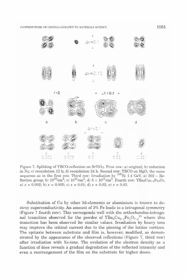
Figure 7. Splitting ofYBCO-reflection on SrTi03. First row: a) original; b) reductionin N2; c) reoxidation 12 h; d) reoxidation 24 h. Second row: YBCO on MgO, the samesequence as in the first row. Third row: Irradiation by 209Bi 1.4 GeV, a) 302 - Re-
. 10 2 11 2 11 2flection group; b) 10 Icm; c) 10 Icm; d) 5 x 10 Icm. Fourth row: YBa2Cu3-xFex07,a) x = 0.002; b) x = 0.005; c) x = 0.01; d) x = 0.02; e) x = 0.03.
Substitution of Cu by other 3d-elements or aluminium is known to de-stroy superconductivity. An amount of 3%Fe leads to a tetragonal symmetry(Figure 7 fourth row). This corresponds well with the orthorhombic-tetrago-nal transition observed for the powder of YBa2Cu3_xFex07_/5where thistransition has been observed for similar values. Irradiation by heavy ionsmay improve the critical current due to the pinning of the lattice vortices.The epitaxie between substrate and film is, however, modified, as demon-strated by the appearance of the observed reflections (Figure 7, third row)after irradiation with Xe-ions. The evolution of the electron density as afunction of dose reveals a gradual degradation of the reflected intensity andeven a rearrangement of the film on the substrate for higher doses.
1062 H. FUESS
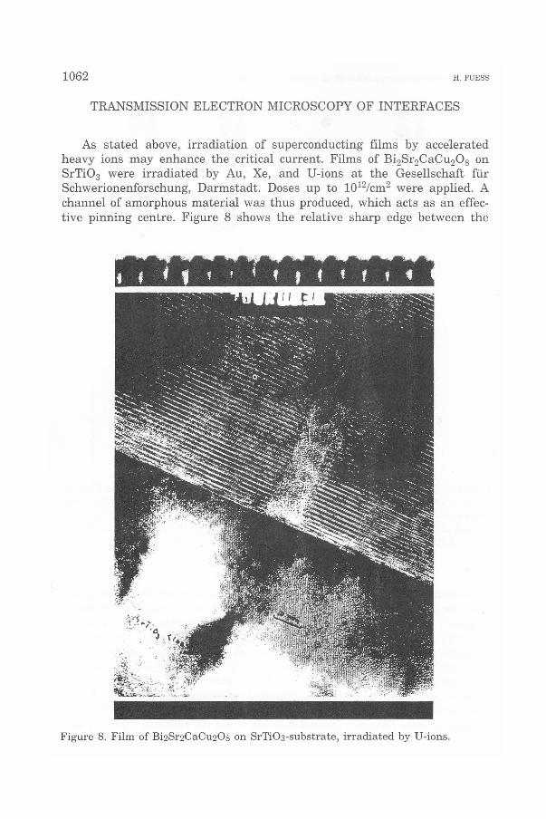
TRANSMISSION ELECTRON MICROSCOPY OF INTERFACES
As stated above, irradiation of superconducting films by acceleratedheavy ions may enhance the critical current. Films of Bi2Sr2CaCu20S onSrTi03 were irradiated by Au, Xe, and U-ions at the Gesellschaft furSchwerionenforschung, Darmstadt. Doses up to 1012/cm2were applied. Achannel of amorphous material was thus produced, which acts as an effec-tive pinning centre. Figure 8 shows the relative sharp edge between the
. -t ff, l f 4 t,«", 11
Figure 8. Film of Bi2Sr2CaCu20s on Sr'I'rOs-substratc, irradiated by U-ions.
CONTRIBUTIONS OF CRYSTALLOGRAPHY TO MATERIALS SCIENCE 1063
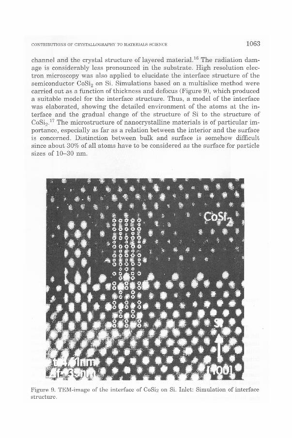
channel and the crystal structure of layered material.l" The radiation dam-age is considerably less pronounced in the substrate. High resolution elec-tron microscopy was also applied to elucidate the interface structure of thesemiconductor CoSi2 on Si. Simulations based on a multislice method werecarried out as a function ofthickness and defocus (Figure 9), which produceda suitable model for the interface structure. Thus, a model of the interfacewas elaborated, showing the detailed environment of the atoms at the in-terface and the gradual change of the structure of Si to the structure ofCoSi2Y The microstructure of nanocrystalline materials is of particular im-portance, especially as far as arelation between the interior and the surfaceis concerned. Distinction between bulk and surface is somehow difficultsince about 30% of all atoms have to be considered as the surface for particlesizes of 10-30 nm.
Figure 9. TEM-image of the interface of COSi2on Si. InIet: Simulation of interfacestructure.
1064 H. FUESS
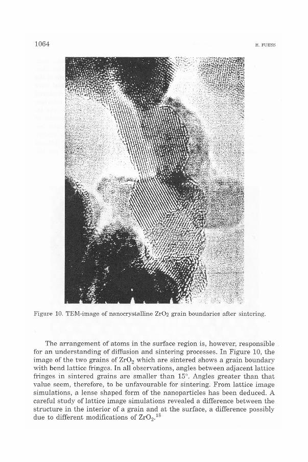
Figure 10. TEM-image of nanocrystalline Zr02 grain boundaries after sintering.
The arrangement of atoms in the surface region is, however, responsiblefor an understanding of diffusion and sintering processes. In Figure 10, theimage of the two grains of Zr02 which are sintered shows a grain boundarywith bend lattice fringes. In all observations, angles between adjacent latticefringes in sintered grains are smaller than 15°. Angles greater than thatvalue seem, therefore, to be unfavourable for sintering. From lattice imagesimulations, a lense shaped form of the nanoparticles has been deduced. Acareful study of lattice image simulations revealed a difference between thestructure in the interior of a grain and at the surface, a difference possiblydue to different modifications of Zr02.18
CONTRIBUTIONS OF CRYSTALLOGRAPHY TO MATERIALS SCIENCE 1065
MAGNETIC PROPERTIES OF SUPERCONDUCTORS
The copper ions in yttrium barium cuprate (YBCO)occupy two differentcrystallographic sites, which are named Cu(l) and Cu(2) in the literature.The crystal chemistry of this system has been discussed in many details andwill not be repeated here. Substitution of Cu by other 3d-elements (Fe, Co,Ni) or trivalent cations like Al takes place in most cases in the CufLl-posi-tion. The magnetic ordering of Cu in YBCO was established, and an antif-erromagnetic spin arrangement was detected. Furthermore, a phase transi-tion from one antiferromagnetic structure (AF 1) to another at lowtemperature (AF II) was reported. Careful neutron diffraction studies on anAl-doped single crystal of YBCO and on a crystal of undoped material wererecently carried out by our group in collaboration with Riso National Labo-
AFI
0.49 O.S 0.51 052
K=(q"q,,2)
AFII
~~ 400
>,
o'§ 200
~1~-;:l:~ Cu(')
\ C""-/......L Cu(l)
~ot::: 600
O~L-L-L-L-L-L-~O.4S 0.49 0.5 O.5J 0.52
K =(q"q,,~)
eu(2)
Cu+ (3d10)
CuO)
I - Cu2+ (3d'l)
Cu(2) -
Cu(l) (frj- 1C"(I)1jtI n
Cu(2) -
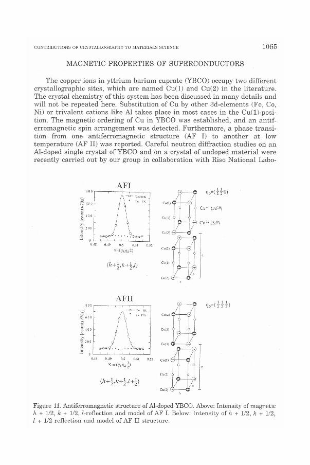
Figure 11.Antiferromagnetic structure of Al-doped YBCO.Ahove: Intensity of magnetich + 112,k + 112,l-ref1ection and model of AF 1. Below: Intensity of h + 1/2, k + 1/2,l + 112ref1ection and model of AF II structure.
1066 !-l. FUESS
ratory in Denmark. It was demonstrated that the magnetic phase transitiononly occurs for the doped material.l'' No such transition was observed forthe undoped material/? in contra st to previous reports. The only possible ex-planation for that finding is the conclusion that the material previously de-scribed was most probably contaminated by Al which occurred in those ma-terials as a consequence of crystal growth in corundum crucibles.
The magnetic structure of the doped material is presented in Figure 11for the two phases. Only Cu(2)-atoms are involved and carry a magnetic mo-ment of Il ~0.5 f..lB' No moment of Cu(l) is observed and an examination ofthe intensity of the nonmagnetic reflections by neutron and X-ray reflectionsrevealed areplacement of Cu(l) by Al atoms. As Al possibly can not adaptto the line ar chain arrangement of Cu(l) but prefers tetrahedral environ-ment, a cluster model for the Al ordering has been proposed which has beenchecked for various oxidation-reduction conditions.F'
CONCLUSION
Crystallographic techniques and methods have a considerable impact onthe precise determination of structural details. As the details of the micro-structure influence physical and chemical properties of materials to a greatextent, crystallographic methods have to be developed further in all fieldsof materials science.
Acknowledgement. - The work presented has been supported by the DeutscheForschungsgemeinschaft, the Bundesminister fur Forschung und Technologie andthe Fonds der Chemischen Industrie, Germany.
REFERENCES
1. H. Fuess, in: Forschung mit Rontgenstrahlen, F. H. W. Heuck u. E. Macherauch(Eds.), Springer-Verlag Heidelberg, 1995, pp. 386--401.
2. R. Schnell and H. Fuess, Ber. Bunsenges. Phys. Chem. 100 (1996) 578-584.3. R. Hoppe, G. Schulz-Ekloff, D. Wohrle, C. Kirschhock, H. Fuess, 1. Uytterhoeven,
and R. A. Schoonheydt, Adu. Materials 7 (1995) 61-64.4. J. Care, C. Finger, J. Richter-Mendau, L. Werner, and B. Zibrowius, Adu. Mate-
rials 4 (1992) 273-276. .5. V. Kaučič, Croat. Chem. Acta 67 (1994) 241-287.6. C. Kirschhock and H. Fuess, Zeolites, in press.7. H. Klein, C. Kirschhock, and H. Fuess, J. Phys. Chem. 98 (1994) 12345-12360.8. C. Kirschhock and H. Fuess, Microporous Materials 2 (1994) 261-267.9. M. Czjzek, H. Jobic, and M. Bee, J. Chem. Soc, Faraday Trans. 87 (1991) 3455-3459.
10. T. Pirling, PhD-Thesis, Technical University, Darmstadt, 1995.11. F. -Iahrling and H. Fuess, unpublished resuIts.12. B. Schulte, M. Maul, W. Becker, H. G. Schlosser, S. Elschner, P. Hausler, and H.
Adrian, Appl. Phys. LeU. 59 (1991) 869-873.
CONTRIBUTIONS OF CRYSTALLOGRAPHY TO MATERIALS SCIENCE 1067
13. C. Tome-Rosa, G. Jakob, M. Maul, A. Walkenhorst, M. Schmidt, P. Wagner, P.Przyslupski, and H. Adrian, Physica Cl71 (1991) 231-235.
14. T. Steinborn, H. Adrian, E. Brecht, H. Fuess, M. Maul, G. Miehe, K. Petersen, M.Rao, W.Schmahl, M. Schmitt, C. Traeholt, J. Wiesner, G. Wirth, H. Zandbergen,and J. Zegenhagen, J. Appl. Crystallogr. 29 (1996) 125-133.
15. Y.Ren, W.Schmahl, E. Brecht, and H. Fuess, Physica C199 (1992) 414-424.16. J. Wiesner, C. Traeholt, J. Wen, H. Zandbergen, G. Wirth, H. Fuess, Physica C268
(1996)161-172.17. M. Rodewald, Unpublished ResuIts.18. G. Nitsche, M. Rodewald, G. Skandan, H. Fuess, and H. Hahn, Nanocryst. Mate-
rials 7 (1996) 535-546.19. E. Brecht, W. Schmahl, H. Fuess, H. Casalta, P. Schleger, B. Lebech, N. H. An-
dersen, and Th. Wolf,Phys. Reu. B52 (1995) 9601-9610.20. H. Casalta, P. Schleger, E. Brecht, W.Montfrooig, N. H. Andersen, B. Lebech, W.
Schmahl, H. Fuess, R. Liang, W. N. Hardy, and Th. Wolf,Physica C235 (1994)1623-1624.
21. E. Brecht, W.W.Schmahl, G. Miehe, M. Rodewald, H. Fuess, N. H. Andersen, J.HanBmann, and Th. Wolf,Physica C265 (1996) 53-66.
SAŽETAK
Doprinos kristalografije znanosti o materijalima
Hartmut Fuess
Svojstva materijala važnih u raznim područjima znanosti i tehnike izravno ovise omikrostrukturi. Kristalografija je znanstvena grana u okviru koje se istražuje mikro-struktura tvari i materijala raznolikim difrakcijskim i spektroskopskim metodama.
U radu se navodi nekoliko primjera iz okvira istraživanja materijala u Tehničkojvisokoj školi u Darmstadtu. Pomoću rentgenske i neutronske difrakcije te spektro-skopije NMR ineelastičnog raspršenja neutrona istražuje se struktura i dinamikaaromatskih molekula u katalitičkim aktivnim zeolitima.
Površine i granične plohe poluvodiča i tankih poluvodičkih filmova proučavajuse u difrakcijskim metodama, gdje upadno zračenje zatvara mali kut s površinom.Analizom difrakcijske slike izvode se podaci o debljini i faznom sastavu tankog filmai o reljefu površine.
Pomoću transmisijske elektronske mikroskopije (TEM) dobivaju se dodatni po-daci o strukturi graničnih ploha, posebnom primjenom simulirajućih slika uzorka po-dijeljenog u slojeve. Prikazano je istraživanje tankih filmova COSi2na Si te LaB6 naGaAs, uz njihovu modifikaciju zamjenom iona. Opisuje se i povećanje tvrdoćepovršinskog sloja čelika primjenom implantacije iona (ugljik, dušik). Difrakcijskimmetodama, gdje upadno zračenje zatvara mali kut s površinom uzorka, dobivaju sepodaci o stvaranju raznih karbida pri različitim dubinama u uzorku. U supravodi-čkim filmovima Bi2Sr2CaCu20s na SrTi03 povećana je gustoća električne struje zared veličine uvođenjem praznina (ozračivanje sa (Xe, Au, U)). Primjenom TEMopaženi su amorfni stupci u uzorku, s jasnim granicama između tih stupaca i neoz-načenog dijela uzorka.