Embed Size (px)
Citation preview
Controllable p-n Junction Formation inMonolayer Graphene Using ElectrostaticSubstrate EngineeringHsin-Ying Chiu,* Vasili Perebeinos, Yu-Ming Lin, and Phaedon Avouris*
IBM Thomas J. Watson Research Center, Yorktown Heights, New York 10598, United States
ABSTRACT We investigate electric transport in graphene on SiO2 in the high field limit and report on the formation of p-n junctions.Previously, doping of graphene has been achieved by using multiple electrostatic gates, or charge transfer from adsorbants. Here wedemonstrate a novel approach to create p-n junctions by changing the local electrostatic potential in the vicinity of one of the contactswithout the use of extra gates. The approach is based on the electronic modification not of the graphene but of the substrate andproduces a well-behaved, sharp junction whose position and height can be controlled.
KEYWORDS Graphene, transistor, p-n junction, high-field transport, trap charges, substrate
While the low field carrier transport in graphene hasalready been the focus of numerous studies,1-6 thebehavior of graphene devices in the high field
limit has received much less attention.7-12 Thus, while it wasshown that graphene itself can withstand current densitiesapproaching 109 A/cm2,13,14 the behavior of graphene de-vices at high fields still remains largely unexplored. However,for nanoelectronic applications the interest is in the high fieldtransport regime since devices are usually operated at ornear the current saturation limit. Currently, little is knownabout graphene under those conditions. In this paper, westudy the high field regime and show that while grapheneitself is stable, there are crucial changes induced in the gatedielectrics that strongly affect the transport in graphenechannel. This effect is enhanced in the atomic-layer thinbody of the graphene channel. Thus, conclusions about thebehavior of devices at high bias need to be carefully exam-ined. Most importantly, we show that the electrostaticmodifications of the substrate can be exploited to create anabrupt graphene p-n junction, which offers opportunitiesextending beyond CMOS technology, such as planar electronVeselago lenses.15 The process is controllable and we createthese junctions with desired lengths and barrier heightswithout resorting to the use of multiple gates,7,16-23 orcharge transfer from adsorbates,24-26 as is currently thecase.
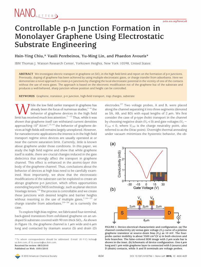
To explore high bias regime, we fabricated four-terminal,back-gated transistors from exfoliated graphene on an un-doped Si substrate covered with 90 nm thick SiO2. As shownin Figure 1b, the graphene channel is 1 µm wide and 6 µmlong and contacted by titanium source (S) and drain (D)
electrodes.27 Two voltage probes, A and B, were placedalong the channel separating it into three segments (denotedas SA, AB, and BD) with equal lengths of 2 µm. We firstconsider the case of p-type (hole) transport in the channelby choosing negative drain (VD < 0) and gate voltages (VG -VCNP < 0, where VCNP is the charge neutrality point, alsoreferred to as the Dirac point). Overnight thermal annealingunder vacuum minimizes the hysteretic behavior, the ob-
* To whom correspondence should be addressed. E-mail: (H.-Y.C) [email protected]; (P.A) [email protected] for review: 08/5/2010Published on Web: 10/01/2010
FIGURE 1. Device electrical characteristic and configuration. (a) Thechannel conductivity (σ) versus gate voltage (VG) curve of a pristinegraphene transistor at source-drain bias (VD) as 10 mV. The four-probe carrier mobility is about 3500 cm2/(V s) in both electron andhole branches. The false-colored SEM image with 2 µm scale bar isshown in the inset. (b) Schematic of device configuration. One 6 µmlong and 1 µm wide graphene layer is connected with S (source) andD (drain) contacts, while A and B terminals are voltage probes.
pubs.acs.org/NanoLett
© 2010 American Chemical Society 4634 DOI: 10.1021/nl102756r | Nano Lett. 2010, 10, 4634–4639
served clean “V” shape characteristic and a nearly zero VCNP
in Figure 1a signify negligible unintentional doping28 includ-ing water molecules29 and good channel uniformity in theinitial device. A doping profile along the channel is thencreated by applying a large drain bias, up to -10 V, toelectrically stress the devices. We have systematically variedthe extent of the electrical stress by applying different gatevoltages. The amount of doping induced by the high-fieldstress can subsequently be inferred from the change of VCNP
in a ID-VG gate sweep performed at low bias. Therefore, inthis work, each high-bias measurement is followed by a low-bias gate sweep as a monitoring routine.
Our experimental procedure involves to first sweep VD
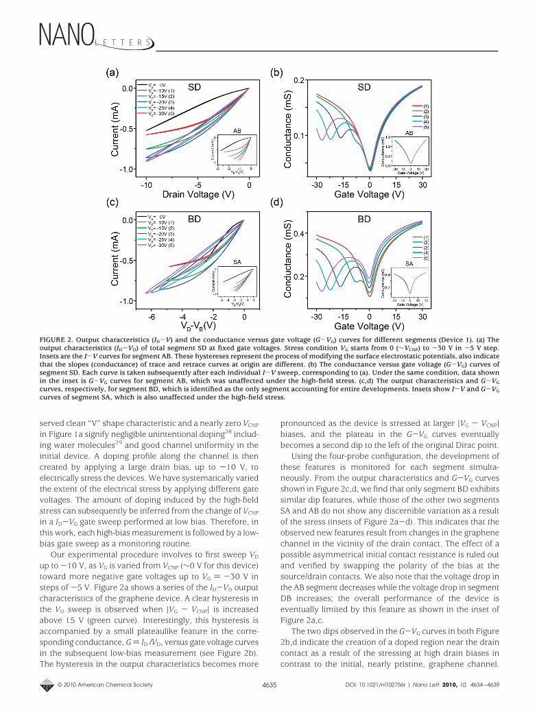
up to -10 V, as VG is varied from VCNP (∼0 V for this device)toward more negative gate voltages up to VG ) -30 V insteps of -5 V. Figure 2a shows a series of the ID-VD outputcharacteristics of the graphene device. A clear hysteresis inthe VD sweep is observed when |VG - VCNP| is increasedabove 15 V (green curve). Interestingly, this hysteresis isaccompanied by a small plateaulike feature in the corre-sponding conductance, G ) ID /VD, versus gate voltage curvesin the subsequent low-bias measurement (see Figure 2b).The hysteresis in the output characteristics becomes more
pronounced as the device is stressed at larger |VG - VCNP|biases, and the plateau in the G-VG curves eventuallybecomes a second dip to the left of the original Dirac point.
Using the four-probe configuration, the development ofthese features is monitored for each segment simulta-neously. From the output characteristics and G-VG curvesshown in Figure 2c,d, we find that only segment BD exhibitssimilar dip features, while those of the other two segmentsSA and AB do not show any discernible variation as a resultof the stress (insets of Figure 2a-d). This indicates that theobserved new features result from changes in the graphenechannel in the vicinity of the drain contact. The effect of apossible asymmetrical initial contact resistance is ruled outand verified by swapping the polarity of the bias at thesource/drain contacts. We also note that the voltage drop inthe AB segment decreases while the voltage drop in segmentDB increases; the overall performance of the device iseventually limited by this feature as shown in the inset ofFigure 2a,c.
The two dips observed in the G-VG curves in both Figure2b,d indicate the creation of a doped region near the draincontact as a result of the stressing at high drain biases incontrast to the initial, nearly pristine, graphene channel.
FIGURE 2. Output characteristics (ID-V) and the conductance versus gate voltage (G-VG) curves for different segments (Device 1). (a) Theoutput characteristics (ID-VD) of total segment SD at fixed gate voltages. Stress condition VG starts from 0 (∼VCNP) to -30 V in -5 V step.Insets are the I-V curves for segment AB. These hystereses represent the process of modifying the surface electrostatic potentials, also indicatethat the slopes (conductance) of trace and retrace curves at origin are different. (b) The conductance versus gate voltage (G-VG) curves ofsegment SD. Each curve is taken subsequently after each individual I-V sweep, corresponding to (a). Under the same condition, data shownin the inset is G-VG curves for segment AB, which was unaffected under the high-field stress. (c,d) The output characteristics and G-VG
curves, respectively, for segment BD, which is identified as the only segment accounting for entire developments. Insets show I-V and G-VG
curves of segment SA, which is also unaffected under the high-field stress.
© 2010 American Chemical Society 4635 DOI: 10.1021/nl102756r | Nano Lett. 2010, 10, 4634-–4639
Furthermore, the position of the second dip depends on thegate voltage VG used during the stressing, while the originalDirac point stays unaffected. In Figure 3b, we plot the gatevoltages corresponding to these two conductance minimaas a function of the applied VG during the stress. Theunvarying position of the main dip corresponds to theoriginal, unaffected graphene domain in the channel, whilethe progressive evolution of the second dip demonstratesthe correlation between the stress condition and the dopingof the channel and the control that the stress voltageprovides. We tested twelve devices with the same devicegeometry and the same result was observed. We thusconclude that the two dips (Dirac points) are topologicallywell-defined and can be controlled by the applied stressvoltage VG. The position of the second Dirac point relativeto the initial one indicates the generation of positive chargesclose to the drain contact. The observation of these twodistinct and well-defined dips indicates that the graphene isunlikely to be structurally damaged during stressing. Thisconclusion is further supported by the fact that the doubleDirac feature can be eliminated by overnight thermal an-nealing in vacuum at 475 K and the original characteristicsrecovered with VCNP ≈ 0 V. The other possibility of field-induced accumulation associated with mobile charges (suchas alkali atom contaminants) is also not likely, due to theabsence of observable hysteresis in the original device and,most importantly, the fact that the application of stressvoltages with the opposite polarity does not affect the doubledip structure. Therefore, the above observations and theknown properties of insulators under stress30 strongly sug-gest that trapped charge in the silicon oxide substrate is the
source of the local doping under high bias conditions. Theelectron affinity energy and the band gap of silicon oxideare 0.95 and 8.9 eV, respectively,31 while the graphene workfunction is ∼4.5 eV.32 Therefore, the barriers for an electronor hole to be injected into bulk traps in SiO2 are ∼3.6 and∼4.3 eV, respectively. These energies are too high to accountfor our observations. In addition, the leakage current intothe back-gate remains constant and in the few picoampsrange throughout the entire drain voltage sweep. Thus, weattribute the positive charges to trapped charge sites withenergies within the SiO2 bandgap and in the vicinity of thegraphene/oxide interface.
To investigate whether there is charge carrier type prefer-ence for trapping in these sites, we performed similarstressing studies under n-type (electron) transport conditions(i.e., VD > 0, VG - VCNP > 0) in other graphene devices withidentical layouts. Contrary to the case of p-type transport,no new dip was observed even at higher current densities,except for a slight hysteresis in the output characteristics thatis likely due to joule-heating and the modification of surfacechemistry after current annealing.14,33-36 Therefore, undersimilar stress conditions, hole carriers are much easier tobe injected into the traps than electrons, which indicates thatthe processed silicon oxide surface tends to be donorlike(that is, positively charged when empty and neutral whenfilled with an electron).
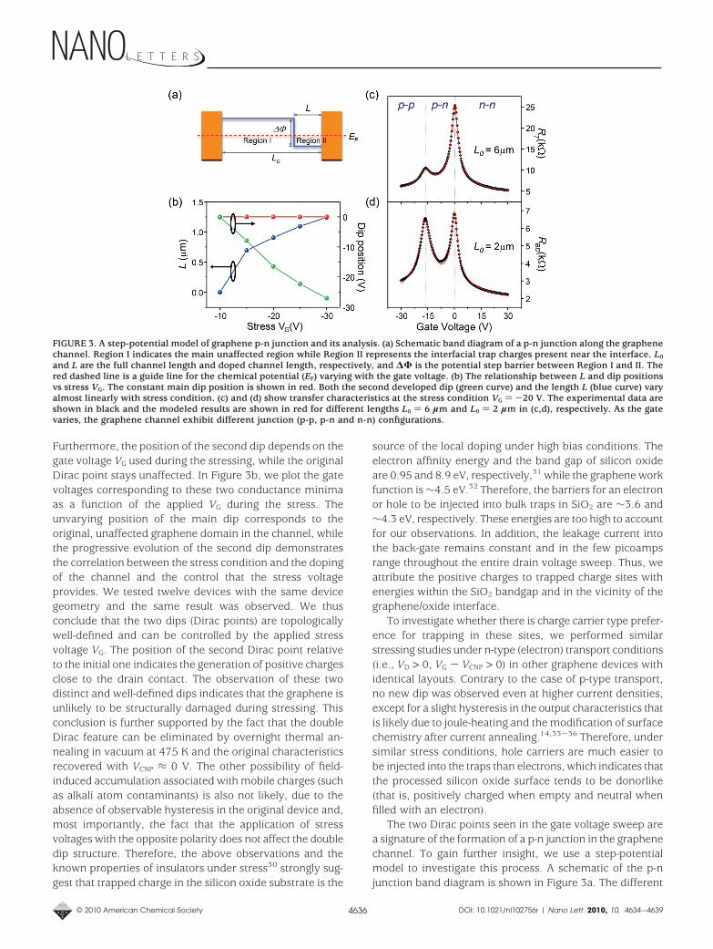
The two Dirac points seen in the gate voltage sweep area signature of the formation of a p-n junction in the graphenechannel. To gain further insight, we use a step-potentialmodel to investigate this process. A schematic of the p-njunction band diagram is shown in Figure 3a. The different
FIGURE 3. A step-potential model of graphene p-n junction and its analysis. (a) Schematic band diagram of a p-n junction along the graphenechannel. Region I indicates the main unaffected region while Region II represents the interfacial trap charges present near the interface. L0
and L are the full channel length and doped channel length, respectively, and ∆Φ is the potential step barrier between Region I and II. Thered dashed line is a guide line for the chemical potential (EF) varying with the gate voltage. (b) The relationship between L and dip positionsvs stress VG. The constant main dip position is shown in red. Both the second developed dip (green curve) and the length L (blue curve) varyalmost linearly with stress condition. (c) and (d) show transfer characteristics at the stress condition VG ) -20 V. The experimental data areshown in black and the modeled results are shown in red for different lengths L0 ) 6 µm and L0 ) 2 µm in (c,d), respectively. As the gatevaries, the graphene channel exhibit different junction (p-p, p-n and n-n) configurations.
© 2010 American Chemical Society 4636 DOI: 10.1021/nl102756r | Nano Lett. 2010, 10, 4634-–4639
electrostatic potential in Region II is due to the interfacialcharges induced by the high field stress described above,which gives rise to the electrostatic potential step relative tothe unperturbed Region I. We note that this is the first timea controllable junction was generated in a graphene channelwithout resorting to multiple gates7,16-23 or chemicaldoping.24-26
The total channel resistance (RT) can be written as (seeSupporting Information)
where RC is the contact resistance, assumed to be gateindependent, with the gate affecting the carrier numbers inregions I and II as (n0
2 + n[VG*]2)1/2.37 The parameters A andB are related to the mobilities µ1 and µ2, and residualelectron-hole puddle densities n01 and n02 by A ) (L0 - L)/(e W µ1) and B ) L/(e W µ2). The carrier densities in thesetwo regions are determined by the electrostatic potential asen1 ) VG*Cox and en2 ) CoxVG* + enit, where VG* ) VG - VCNP
and nit is the trap charge density. The latter can be inferredfrom the measured gate voltage difference ∆V between thetwo resistance maxima as enit ) Cox∆V. From the low-biasresistance measurements in segments SD and BD of lengthL0 ) 6 and 2 µm correspondingly, and the length L of RegionII can be deduced from the following relation A6/A2 ) (6 -L)/(2 - L),38 which is insensitive to the mobility value µ1.
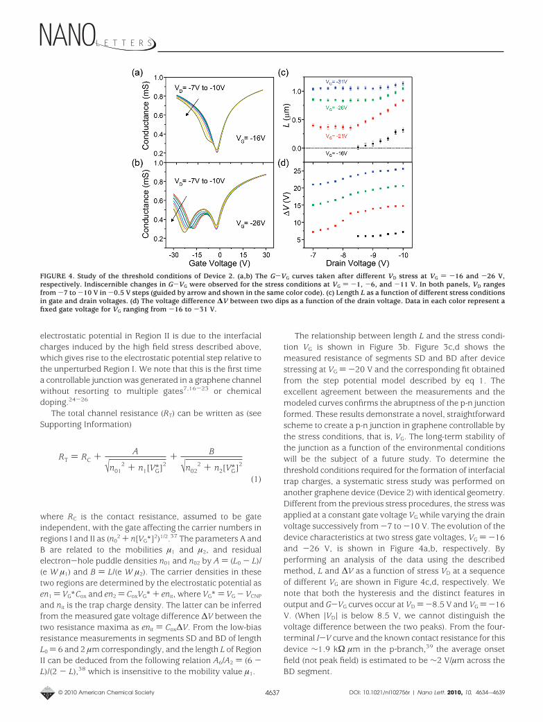
The relationship between length L and the stress condi-tion VG is shown in Figure 3b. Figure 3c,d shows themeasured resistance of segments SD and BD after devicestressing at VG ) -20 V and the corresponding fit obtainedfrom the step potential model described by eq 1. Theexcellent agreement between the measurements and themodeled curves confirms the abruptness of the p-n junctionformed. These results demonstrate a novel, straightforwardscheme to create a p-n junction in graphene controllable bythe stress conditions, that is, VG. The long-term stability ofthe junction as a function of the environmental conditionswill be the subject of a future study. To determine thethreshold conditions required for the formation of interfacialtrap charges, a systematic stress study was performed onanother graphene device (Device 2) with identical geometry.Different from the previous stress procedures, the stress wasapplied at a constant gate voltage VG while varying the drainvoltage successively from -7 to -10 V. The evolution of thedevice characteristics at two stress gate voltages, VG ) -16and -26 V, is shown in Figure 4a,b, respectively. Byperforming an analysis of the data using the describedmethod, L and ∆V as a function of stress VD at a sequenceof different VG are shown in Figure 4c,d, respectively. Wenote that both the hysteresis and the distinct features inoutput and G-VG curves occur at VD )-8.5 V and VG )-16V. (When |VD| is below 8.5 V, we cannot distinguish thevoltage difference between the two peaks). From the four-terminal I-V curve and the known contact resistance for thisdevice ∼1.9 kΩ µm in the p-branch,39 the average onsetfield (not peak field) is estimated to be ∼2 V/µm across theBD segment.
FIGURE 4. Study of the threshold conditions of Device 2. (a,b) The G-VG curves taken after different VD stress at VG ) -16 and -26 V,respectively. Indiscernible changes in G-VG were observed for the stress conditions at VG ) -1, -6, and -11 V. In both panels, VD rangesfrom -7 to -10 V in -0.5 V steps (guided by arrow and shown in the same color code). (c) Length L as a function of different stress conditionsin gate and drain voltages. (d) The voltage difference ∆V between two dips as a function of the drain voltage. Data in each color represent afixed gate voltage for VG ranging from -16 to -31 V.
RT ) RC + A
√n012 + n1[VG*]2
+ B
√n022 + n2[VG*]2
(1)
© 2010 American Chemical Society 4637 DOI: 10.1021/nl102756r | Nano Lett. 2010, 10, 4634-–4639
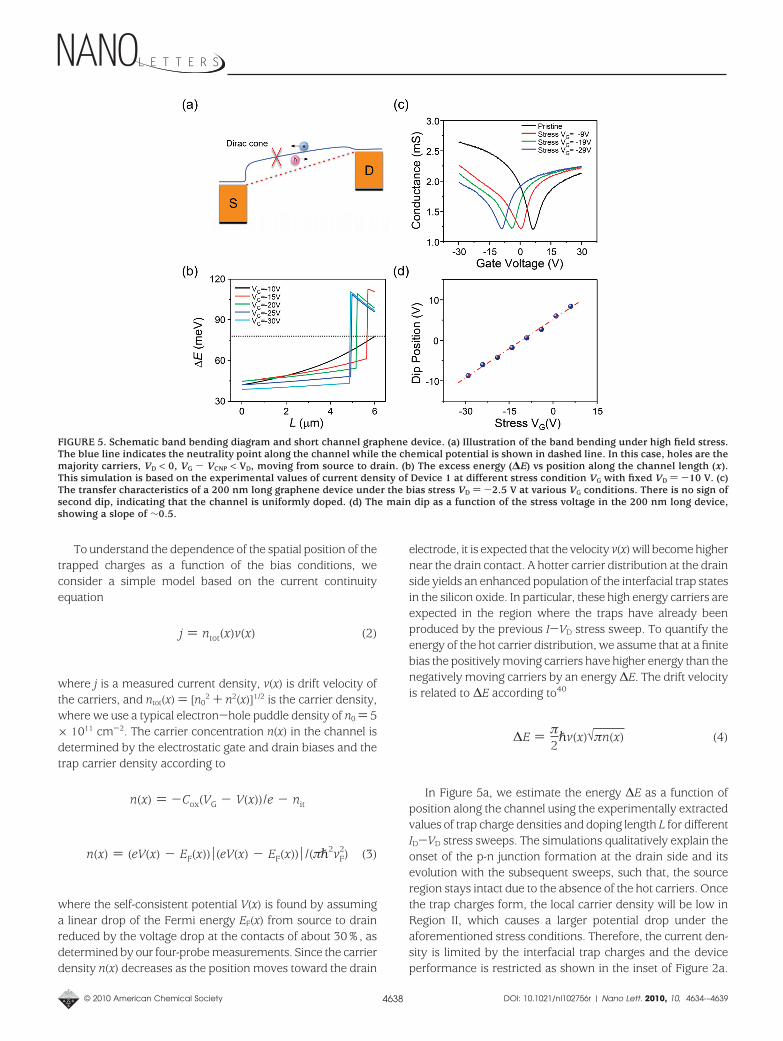
To understand the dependence of the spatial position of thetrapped charges as a function of the bias conditions, weconsider a simple model based on the current continuityequation
where j is a measured current density, v(x) is drift velocity ofthe carriers, and ntot(x) ) [n0
2 + n2(x)]1/2 is the carrier density,where we use a typical electron-hole puddle density of n0 ) 5× 1011 cm-2. The carrier concentration n(x) in the channel isdetermined by the electrostatic gate and drain biases and thetrap carrier density according to
where the self-consistent potential V(x) is found by assuminga linear drop of the Fermi energy EF(x) from source to drainreduced by the voltage drop at the contacts of about 30%, asdetermined by our four-probe measurements. Since the carrierdensity n(x) decreases as the position moves toward the drain
electrode, it is expected that the velocity v(x) will become highernear the drain contact. A hotter carrier distribution at the drainside yields an enhanced population of the interfacial trap statesin the silicon oxide. In particular, these high energy carriers areexpected in the region where the traps have already beenproduced by the previous I-VD stress sweep. To quantify theenergy of the hot carrier distribution, we assume that at a finitebias the positively moving carriers have higher energy than thenegatively moving carriers by an energy ∆E. The drift velocityis related to ∆E according to40
In Figure 5a, we estimate the energy ∆E as a function ofposition along the channel using the experimentally extractedvalues of trap charge densities and doping length L for differentID-VD stress sweeps. The simulations qualitatively explain theonset of the p-n junction formation at the drain side and itsevolution with the subsequent sweeps, such that, the sourceregion stays intact due to the absence of the hot carriers. Oncethe trap charges form, the local carrier density will be low inRegion II, which causes a larger potential drop under theaforementioned stress conditions. Therefore, the current den-sity is limited by the interfacial trap charges and the deviceperformance is restricted as shown in the inset of Figure 2a.
FIGURE 5. Schematic band bending diagram and short channel graphene device. (a) Illustration of the band bending under high field stress.The blue line indicates the neutrality point along the channel while the chemical potential is shown in dashed line. In this case, holes are themajority carriers, VD < 0, VG - VCNP < VD, moving from source to drain. (b) The excess energy (∆E) vs position along the channel length (x).This simulation is based on the experimental values of current density of Device 1 at different stress condition VG with fixed VD ) -10 V. (c)The transfer characteristics of a 200 nm long graphene device under the bias stress VD ) -2.5 V at various VG conditions. There is no sign ofsecond dip, indicating that the channel is uniformly doped. (d) The main dip as a function of the stress voltage in the 200 nm long device,showing a slope of ∼0.5.
j ) ntot(x)v(x) (2)
n(x) ) -Cox(VG - V(x))/e - nit
n(x) ) (eV(x) - EF(x))|(eV(x) - EF(x))|/(πp2vF2) (3)
∆E ) π2pv(x)√πn(x) (4)
© 2010 American Chemical Society 4638 DOI: 10.1021/nl102756r | Nano Lett. 2010, 10, 4634-–4639
As shown in Figure 4c, the length of the doped Region IIcan be extended to be as long as 1 µm. This indicates thatfor a shorter channel device, the entire graphene channelcould be doped, causing a smooth shift of the Dirac pointinstead of the occurrence of two resistance maxima. Toverify this uniform doping effect in a short channel device,a two-terminal graphene device with 200 nm channel lengthwas fabricated. Following similar procedures for creating ann-doped junction, we find that the transfer characteristicsremain dominated by only a single Dirac point, which shiftstoward negative voltages, as shown in Figure 5c. The Diracposition depends linearly on the stress gate voltage, asshown in Figure 5d. This result indicates that we achieveduniform charging of the interfacial traps along the channelin a short-channel device.
In conclusion, we have shown that a sharp p-n junction canbe produced in monolayer graphene device structures throughthe electrostatic modification of the gate insulator surface.Furthermore, we demonstrated the ability of controlling boththe length and the potential difference of the doped regionalong the graphene transistor channel. This novel approach toproduce a well-defined p-n junction without extra gates oradsorbates opens up new opportunities for studying quantumtransport in graphene devices and the results provide newinsight into the phenomena that can take place at the high fieldtransport limit, also demonstrating the need to clearly distin-guish between substrate-induced effects and the intrinsic high-field transport behavior of graphene.
Acknowledgment. We thank B. Ek, J. Bucchignano, andG. Wright for expert technical assistance. We also thankJames Stathis, Marcus Freitag, Marc Bockrath, Shu-Jen Han,Damon Farmer, Ching-Tzu Chen, Wenjuan Zhu, and Yan-qing Wu for helpful discussions. This work was supportedby DARPA under Contract FA8650-08-C-7838 through theCERA program. The views, opinions, and/or findings con-tained in this article are those of the authors and should notbe interpreted as representing the official views or policies,either expressed or implied, of the Defense AdvancedResearch Projects Agency or the Department of Defense.
Supporting Information Available. Details of samplefabrication, electrical measurements, data analysis method,and additional fitting model with e-h puddles. This material isavailable free of charge via the Internet at http://pubs.acs.org.
REFERENCES AND NOTES(1) Geim, A. K. Science 2009, 324 (5934), 1530.(2) Castro Neto, A. H.; Guinea, F.; Peres, N. M. R.; Novoselov, K. S.;
Geim, A. K. Rev. Mod. Phys. 2009, 81 (1), 109.(3) Chen, J.-H.; Jang, C.; Xiao, S.; Ishigami, M.; Fuhrer, M. S. Nat.
Nanotechnol. 2008, 3 (4), 206.(4) Adam, S.; Hwang, E. H.; Galitski, V. M.; Das Sarma, S. Proc. Nat.
Acad. Sci. U.S.A. 2007, 104 (47), 18392.(5) Geim, A. K.; MacDonald, A. H. Phys. Today 2007, 60 (8), 35.(6) Avouris, Ph.; Chen, Z.; Perebeinos, V. Nat. Nanotechnol. 2007, 2
(10), 605.(7) Meric, I.; Han, M. Y.; Young, A. F.; Ozyilmaz, B.; Kim, P.; Shepard,
K. L. Nat. Nanotechnol. 2008, 3 (11), 654.
(8) Luo, X.; Lee, Y.; Konar, A.; Fang, T.; Xing, G.; Snider, G.; Jena, D.Current-carrying Capacity of Long & Short Channel 2D GrapheneTransistors. In 66th Device Research Conference, Santa Barbara,CA, 2008.
(9) Freitag, M.; Steiner, M.; Martin, Y.; Perebeinos, V.; Chen, Z.;Tsang, J. C.; Avouris, Ph. Nano Lett. 2009, 9 (5), 1883.
(10) Barreiro, A.; Lazzeri, M.; Moser, J.; Mauri, F.; Bachtold, A. Phys.Rev. Lett. 2009, 103 (7), No. 076601.
(11) DaSilva, A. M.; Zou, K.; Jain, J. K.; Zhu, J. Phys. Rev. Lett. 2010,104 (23), 236601.
(12) Dorgan, V. E.; Bae, M.-H.; Pop, E. Appl. Phys. Lett. 2010, 97 (8),No. 082112.
(13) Murali, R.; Yang, Y.; Brenner, K.; Beck, T.; Meindl, J. D. Appl. Phys.Lett. 2009, 94 (24), 243114.
(14) Moser, J.; Barreiro, A.; Bachtold, A. Appl. Phys. Lett. 2007, 91 (16),163513.
(15) Cheianov, V. V.; Fal’ko, V.; Altshuler, B. L. Science 2007, 315(5816), 1252.
(16) Williams, J. R.; DiCarlo, L.; Marcus, C. M. Science 2007, 317(5838), 638.
(17) Ozyilmaz, B.; Jarillo-Herrero, P.; Efetov, D.; Abanin, D. A.; Levitov,L. S.; Kim, P. Phys. Rev. Lett. 2007, 99 (16), 166804.
(18) Huard, B.; Sulpizio, J. A.; Stander, N.; Todd, K.; Yang, B.; Gold-haber-Gordon, D. Phys. Rev. Lett. 2007, 98 (23), 236803.
(19) Liu, G.; Velasco, J., Jr.; Bao, W.; Lau, C. N. Appl. Phys. Lett. 2008,92 (20), 203103.
(20) Stander, N.; Huard, B.; Goldhaber-Gordon, D. Phys. Rev. Lett.2009, 102 (2), No. 026807.
(21) Velasco, J.; Liu, G.; Jing, L.; Kratz, P.; Zhang, H.; Bao, W.; Bockrath,M.; Lau, C. N. Phys. Rev. B 2010, 81 (12), 121407.
(22) Velasco, J., Jr.; Liu, G.; Bao, W.; Lau, C. N. New J. Phys. 2009, 11(9), No. 095008.
(23) Young, A. F.; Kim, P. Nat. Phys. 2009, 5 (3), 222.(24) Farmer, D. B.; Lin, Y.-M.; Afzali-Ardakani, A.; Avouris, Ph. Appl.
Phys. Lett. 2009, 94 (21), 213106.(25) Lohmann, T.; von Klitzing, K.; Smet, J. H. Nano Lett. 2009, 9 (5), 1973.(26) Brenner, K.; Murali, R. Appl. Phys. Lett. 2010, 96 (6), No. 063104.(27) Two types of metal composition have been used in our study and
show the similar transport behaviors. One is the stack of Ti/Au(20 nm/30 nm) and the other is Ti/Pd/Au (0.5 nm/20 nm/30 nm).In the second case, Ti is used for the adhesion layer.
(28) The estimated residual concentration for this device n0 is∼3.9 × 1011 cm-2.
(29) Kim, W.; Javey, A.; Vermesh, O.; Wang, Q.; Li, Y.; Dai, H. NanoLett. 2003, 3 (2), 193.
(30) Nicollian, E. H.; Brews, J. R. MOS (Metal Oxide Semiconductor)Physics and Technology; Wiley: New York, 1982.
(31) Muller, R. S.; Kamins, T. I.; Chan, M., Device Electronics forIntegrated Circuits: Wiley: New York, 2003.
(32) Giovannetti, G.; Khomyakov, P. A.; Brocks, G.; Karpan, V. M.; vanden Brink, J.; Kelly, P. J. Phys. Rev. Lett. 2008, 101 (2), No. 026803.
(33) Romero, H. E.; Shen, N.; Joshi, P.; Gutierrez, H. R.; Tadigadapa,S. A.; Sofo, J. O.; Eklund, P. C. ACS Nano 2008, 2 (10), 2037.
(34) Carla, M. A.; Pierre, L. L.; Matthieu, P.; Francois, L.; Benoit, C. S.-A.; Patrick, D.; Richard, M. Adv. Mater. 2009, 21 (30), 3087.
(35) Connolly, M. R.; Chiou, K. L.; Smith, C. G.; Anderson, D.; Jones,G. A. C.; Lombardo, A.; Fasoli, A.; Ferrari, A. C. Appl. Phys. Lett.2010, 96 (11), 113501.
(36) Nourbakhsh, A.; Cantoro, M.; Klekachev, A.; Clemente, F.; Soreee,B.; van der Veen, M. H.; Vosch, T.; Stesmans, A.; Sels, B.; DeGendt, S. J. Phys. Chem. C 2010, 114 (15), 6894.
(37) Seyoung, K.; Junghyo, N.; Insun, J.; Davood, S.; Luigi, C.; Zhen,Y.; Emanuel, T.; Sanjay, K. B. Appl. Phys. Lett. 2009, 94 (6), No.062107.
(38) For voltage probing, terminal A and B are set at IA,B ) 0 A andthe voltage reading during the measurement is monitored. Thus,we can extract data between each terminal and compile twodifferent data sets from the same run: one for whole channel,segment SD, and second for segment BD.
(39) We calculate the contact resistance in the following way: Rc,x )1/2(R2p-3R4p),x where x is for either the p-branch or e-branch.
(40) Perebeinos, V.; Avouris, Ph. Phys. Rev. B 2010, 81 (19),195442.
© 2010 American Chemical Society 4639 DOI: 10.1021/nl102756r | Nano Lett. 2010, 10, 4634-–4639
1/4
Supplementary Information
Controllable p-n junction formation in monolayer graphene
using electrostatic substrate engineering
Hsin-Ying Chiu*, Vasili Perebeinos, Yu-Ming Lin, Phaedon Avouris
*
IBM Thomas J. Watson Research Center, Yorktown Heights, New York 10598, USA
To whom correspondence should be addressed. E-mail: (H.-Y.C) [email protected];
(P.A) [email protected]
1. Sample Fabrication
Devices are prepared by mechanically exfoliating Kish graphite (Toshiba Ceremics) on
undoped Si substrate caped with 90 nm of thermal grown oxide. Metal contacts in
graphene devices were fabricated by standard e-beam lithography and lift-off. Typically,
two types of metal composition have been used in our study and show the similar
transport behaviors. One is the stack of Ti/Au (20 nm/30 nm) and the other is Ti/Pd/Au
(0.5 nm/20 nm/30 nm). In the second case, Ti is used for the adhesion layer. Thereafter,
the channel is formed by etching the undesirable graphene area using oxygen plasma by
reactive-ion etching (Unaxis RIE). Prior to any electrical measurement, overnight thermal
annealing at 475K is performed in vacuum (~ 10-6
torr). This process is used to remove
the gas absorbed and water molecules on the graphene surface and also to discharge any
interfacial traps at the graphene-oxide interface.
2. Electrical Measurements
All measurements are completed in a LakeShore probe station at room temperature with
the semiconductor device analyzer (Agilent Technologies B1500A). In the beginning of
measurements, there is only slight hysteresis in the transfer characteristics (I-VG curve),
and the mobility of these as-prepared device is estimated to be 3500 cm2/Vs from the
four-terminal measurement. Characteristic of Device I was shown in Fig. 1(a) and its
estimated residual concentration n0 is ~3.9×10¹¹
cm-2
. The carrier density of graphene can
be tuned by the back-gate electrostatic potential. For the 90 nm-thick silicon oxide with a
dielectric constant of 3.9, the carrier density is given by n ~ 2.4×10¹¹
(VG – VCNP) cm-2
.
3. Data Analysis Method
Four-terminal measurements provide both voltage and current information for each
terminal. A schematic diagram is shown in Fig 1(b). For voltage probing, terminal A and
B are set at IA,B = 0 A and the voltage reading during the measurement is monitored. Thus,
2/4
we can extract data between each terminal and compile two different data sets from the
same run; one for whole channel, segment SD, and second for segment BD.
Our analysis is based on equation (1) and the corresponding schematic potential profile is
shown in Fig 3(a). In the fit we identify the two peak positions as fixed parameters (VCNP
and ∆V). The remaining parameters are obtained from the fitting of the different length
data sets. n01 and n02 are global parameters for the pristine and doped regions in both data
sets. Note that in fitting the resistance RC in the BD region a value twice as small as that
used in Eq. (1) to fit the SD channel, was obtained, as expected.
4. Fitting Model with e-h Puddles
To account for the electron-hole puddle density near the Dirac point in fitting the
experimental resistance a simple analytical model has been proposed in Ref.[37]:
2 2
0 [ ]G
LR
We n n Vµ=
+ (S1)
where L and W are the length and the width of the channel respectively, is a mobility, n0
is the electron-hole puddle concentration, and n is gate dependent charge carrier
concentration. While Eq. (S1) has been found to work well in fitting the experimental
data by several research groups, its extension to the presence of the two Dirac points (Eq.
(1) of the main text) has not been tested yet. Here we show that Eq. (S1) can be derived
from a microscopic model and it is extension to the presence of the two Dirac points in
the channel (Eq. (1) of the main text) reproduces well by the same model.
We assume that there are multiple parallel channels contributing to the current and each
of them can be characterized by its own value of the Dirac point. The energy distribution
of the Dirac points is assumed to be Gaussian:
( )2
1exp
EF E
tt π
= − (S2)
where t is the width of the distribution. The electron ne and hole nh carrier concentrations
can readily be calculated as:
( ) ( )
( ) ( )
22
2 2
1
2
F
t e h f
F
e
E
tn n n dEF E n E E
v
n dEF E n E
π
∞
−∞
∞
= + = = +
=
∫
∫
h
(S3)
3/4
where ( ) ( ) ( )2 2 2
F Fn E E E vπ= − h and EF is the averaged Fermi level. In Fig. 1S (a), we
show that the total carrier density nt dependence on the gate voltage determined by the
charge carrier density ( - ) = e h G G
e n n C V nearly coincides with a simple analytical form
2 2 2 2
0 G Gn n C V e= + , when ( )2 2 2
0 2F
n t vπ= h .
In the presence of two regions with an averaged Dirac position in the second region being
displaced by ∆φ, the energy distribution function is given by:
( )2
2
1exp
EF E
tt
φπ
+ ∆ = −
(S4)
In principle, the electron-hole carrier density in the second region can be different, but we
keep it the same for simplicity. The conductivity of the second region similarly to Eq. (3)
is determined by the carrier concentrations:
( ) ( ) ( )
( ) ( )
22
2 2 2 2 2 2
2 2
1
2
F
t e h F
F
e
E
tn n n dEF E n E E
v
n dEF E n E
φπ
∞
−∞
∞
= + = = + + ∆
=
∫
∫
h
(S5)
The total resistance of the sequential channels is given proportional to:
0 0
2
1
t t
L L L
N L n L n
−= + (S6)
In Fig. 1S (b), we show that the net carrier density N dependence on the gate voltage
determined nearly coincides with a simple analytical form used in Eq. (1) of the main text.
4/4
2.5
2.0
1.5
1.0
0.5
0.0
1/N
(1
0-1
2 c
m2)
1.0
0.8
0.6
0.4
0.2
0.0
1/N
(1
0-1
2 c
m2)
-40 -30 -20 -10 0 10 20 VG (V)
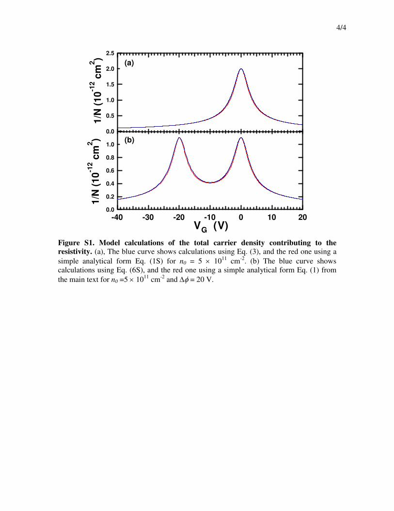
Figure S1. Model calculations of the total carrier density contributing to the
resistivity. (a), The blue curve shows calculations using Eq. (3), and the red one using a
simple analytical form Eq. (1S) for n0 = 5 × 10¹¹
cm-2
. (b) The blue curve shows
calculations using Eq. (6S), and the red one using a simple analytical form Eq. (1) from
the main text for n0 =5 × 10¹¹
cm-2
and ∆φ = 20 V.
(a)
(b)