Embed Size (px)
Citation preview
Coupled quantum electrodynamics in photonic crystal cavities towards controlled phase gate
operations
This article has been downloaded from IOPscience. Please scroll down to see the full text article.
2008 New J. Phys. 10 123013
(http://iopscience.iop.org/1367-2630/10/12/123013)
Download details:
IP Address: 131.151.64.157
The article was downloaded on 12/09/2011 at 21:55
Please note that terms and conditions apply.
View the table of contents for this issue, or go to the journal homepage for more
Home Search Collections Journals About Contact us My IOPscience
T h e o p e n – a c c e s s j o u r n a l f o r p h y s i c s
New Journal of Physics
Coupled quantum electrodynamics in photoniccrystal cavities towards controlled phasegate operations
Y-F Xiao1,2,3, J Gao1, X-B Zou2, J F McMillan1, X Yang1,Y-L Chen2, Z-F Han2, G-C Guo2 and C W Wong1
1 Optical Nanostructures Laboratory, Center for Integrated Science andEngineering, Solid-State Science and Engineering, and Department ofMechanical Engineering, Columbia University, New York, NY 10027, USA2 Key Laboratory of Quantum Information, University of Science andTechnology of China, Hefei 230026, People’s Republic of ChinaE-mail: [email protected] and [email protected]
New Journal of Physics 10 (2008) 123013 (13pp)Received 25 June 2008Published 9 December 2008Online at http://www.njp.org/doi:10.1088/1367-2630/10/12/123013
Abstract. In this paper, a scalable photonic crystal cavity array, in whichsingle embedded quantum dots (QDs) are coherently interacting, is studiedtheoretically. Firstly, we examine the spectral character and optical delay broughtabout by the coupled cavities interacting with single QDs, in an optical analogueto electromagnetically induced transparency. Secondly, we then examine theusability of this coupled QD–cavity system for quantum phase gate operationand our numerical examples suggest that a two-qubit system with fidelity above0.99 and photon loss below 0.04 is possible.
3 Authors to whom any correspondence should be addressed.
New Journal of Physics 10 (2008) 1230131367-2630/08/123013+13$30.00 © IOP Publishing Ltd and Deutsche Physikalische Gesellschaft
2
Contents
1. Introduction 22. Theoretical model 23. Spectral character of coupled QD–cavity arrays 4
3.1. Phase shift and photon storage . . . . . . . . . . . . . . . . . . . . . . . . . . 64. Quantum phase gate operation 75. Gate fidelity and photon loss 116. Conclusion 11Acknowledgments 11References 12
1. Introduction
Cavity quantum electrodynamics (QED) describes a few atoms strongly coupling to quantizedelectromagnetic fields inside an optical cavity. Up to now, it is one of a few experimentallyrealizable systems in which the intrinsic quantum mechanical coupling dominates losses due todissipation, providing an almost ideal system that allows the quantitative study of a dynamicalopen quantum system under continuous observation (for a review, see [1] and referencestherein). Over the past few years, theoretical and experimental studies have mainly focusedon a single cavity interacting with atoms, and tremendous progress has been made rangingfrom strongly trapping single atoms [2] and deterministic generation of single-photon states [3],to observation of atom–photon quantum entanglement [4] and implementation of quantumcommunication protocols [5].
For more applications, current interest lies in the coherent interaction between distantcavities. The coherent interaction of cavity arrays has been studied as an optical analogue toelectromagnetically induced transparency (EIT) in both theory [6, 7] and experiment [8, 9].Coupled cavities can be utilized for coherent optical information storage, because they providealmost lossless guiding and coupling of light pulses at slow group velocities. When dopants suchas atoms or quantum dots (QDs) interact with these cavities, the spatially separated cavitieshave been proposed for implementing quantum logic and constructing quantum networks[10, 11]. Recent studies also show a strong photon-blockade regime and photonic Mott insulatorstate [12], where the two-dimensional hybrid system undergoes a characteristic Mott insulator-to-superfluid quantum-phase transition at zero temperature [13]. Recently, it was shown thatcoupled cavities can also model an anisotropic Heisenberg spin-1/2 lattice in an externalmagnetic field [14]. The character of a coupled cavity configuration has also been studied usingthe photon Green function [15, 16].
2. Theoretical model
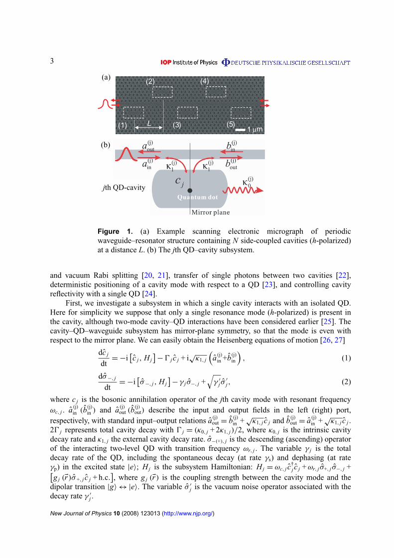
In this paper, using transmission theory, we study coherent interactions in a cavity array thatincludes N cavity–QD subsystems, with indirect coupling between adjacent cavities througha waveguide (figure 1). Recent experimental efforts have reported remarkable progress insolid-state cavities, such as ultra-high quality factors [17]–[19], observation of strong coupling
New Journal of Physics 10 (2008) 123013 (http://www.njp.org/)
3
(1) (3)
(2) (4)
(5)L1 m
(b)
jth QD-cavity
(a)
Figure 1. (a) Example scanning electronic micrograph of periodicwaveguide–resonator structure containing N side-coupled cavities (h-polarized)at a distance L. (b) The jth QD–cavity subsystem.
and vacuum Rabi splitting [20, 21], transfer of single photons between two cavities [22],deterministic positioning of a cavity mode with respect to a QD [23], and controlling cavityreflectivity with a single QD [24].
First, we investigate a subsystem in which a single cavity interacts with an isolated QD.Here for simplicity we suppose that only a single resonance mode (h-polarized) is present inthe cavity, although two-mode cavity–QD interactions have been considered earlier [25]. Thecavity–QD–waveguide subsystem has mirror-plane symmetry, so that the mode is even withrespect to the mirror plane. We can easily obtain the Heisenberg equations of motion [26, 27]
dc j
dt= −i
[c j , H j
]− 0 j c j + i
√κ1, j
(a(j)
in +b(j)in
), (1)
dσ−, j
dt= −i
[σ−, j , H j
]− γ j σ−, j +
√γ ′
j σ′
j , (2)
where c j is the bosonic annihilation operator of the jth cavity mode with resonant frequencyωc, j . a(j)
in (b(j)in ) and a(j)
out (b(j)out) describe the input and output fields in the left (right) port,
respectively, with standard input–output relations a(j)out = b(j)
in +√
κ1, j c j and b(j)out = a(j)
in +√
κ1, j c j .20 j represents total cavity decay with 0 j = (κ0, j + 2κ1, j)/2, where κ0, j is the intrinsic cavitydecay rate and κ1, j the external cavity decay rate. σ−(+), j is the descending (ascending) operatorof the interacting two-level QD with transition frequency ωr, j . The variable γ j is the totaldecay rate of the QD, including the spontaneous decay (at rate γs) and dephasing (at rateγp) in the excited state |e〉; H j is the subsystem Hamiltonian: H j = ωc, j c
†j c j + ωr, j σ+, j σ−, j +[
g j (Er)σ +, j c j + h.c.], where g j (Er) is the coupling strength between the cavity mode and the
dipolar transition |g〉 ↔ |e〉. The variable σ ′
j is the vacuum noise operator associated with thedecay rate γ ′
j .
New Journal of Physics 10 (2008) 123013 (http://www.njp.org/)
4
In the weak excitation limit (excited by a weak monochromatic field or a single-photonpulse with frequency ω), by omitting the term that concerns the Langevin noises [27], the motionequations can be solved, with the transport relation in the frequency domain(
b(j)in (ω)
b(j)out(ω)
)= T j
(a(j)
in (ω)
a(j)out(ω)
). (3)
Here the transport matrix reads
T j =1
α j + κ1, j − 0 j
(−κ1, j α j − 0 j
α j − 0 j + 2κ1, j κ1, j
), (4)
where α j = i1c, j + |g j (Er)|2/(i1r, j − γ j
), 1c, j = ω − ωc, j (1r, j = ω − ωr, j ) represents the
detuning between the input field and the cavity mode (QD transition). For convenience, wealso define the cavity–QD detuning δ j ≡ ωc, j − ωr, j . The transport matrix can be regarded as abasic cell in cascading subsystems and as obtaining the whole transportation for the N-coupledcavity–QD system. The transport properties can thus be expressed as(
b(N)
in (ω)
b(N)out (ω)
)= TN T0 · · · T0T2T0T1
(a(1)
in (ω)
a(1)out(ω)
), (5)
where T0 is the transport matrix via the waveguide with a propagation phase θ . When studyingonly the spectral character of the coupled QD–cavity interaction (section 3), we note that thisis analogous to classical microwave circuit design [28], where the transmission and reflectioncharacteristics from equation (5) can also be examined with coupled-mode theory with dipoleterms inserted. Examining the spectral character first (section 3) helps to understand the coupledQD–cavity controlled quantum phase gate operation and performance (sections 4 and 5).
3. Spectral character of coupled QD–cavity arrays
To examine the physical essence, we need to first examine the spectral character of thecoupled cavity–QD system. The reflection and transmission coefficients are defined as rN1 (ω) ≡
a(1)out (ω) /a(1)
in (ω) and tN1 (ω) ≡ b(N )out (ω) /a(1)
in (ω). In the following, we also assume that thesecavities possess the same dissipation characteristics without loss of generality, i.e. κ0, j = κ0,κ1, j = κ1, κ1 = 50κ0 and 0 j = 0.
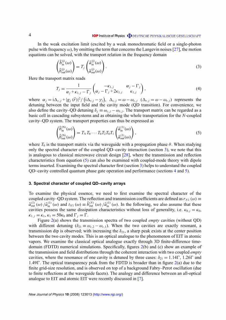
Figure 2(a) shows the transmission spectra of two coupled empty cavities (without QD)with different detuning (δ21 ≡ ωc,2 − ωc,1). When the two cavities are exactly resonant, atransmission dip is observed; with increasing the δ21, a sharp peak exists at the center positionbetween the two cavity modes. This is an optical analogue to the phenomenon of EIT in atomicvapors. We examine the classical optical analogue exactly through 3D finite-difference time-domain (FDTD) numerical simulations. Specifically, figures 2(b) and (c) show an example ofthe transmission and field distributions through the coherent interaction with two coupled emptycavities, where the resonance of one cavity is detuned by three cases: δ21 = 1.140, 1.260 and1.490. The optical transparency peak from the FDTD is broader than in figure 2(a) due to thefinite grid-size resolution, and is observed on top of a background Fabry–Perot oscillation (dueto finite reflections at the waveguide facets). The analogy and difference between an all-opticalanalogue to EIT and atomic EIT were recently discussed in [7].
New Journal of Physics 10 (2008) 123013 (http://www.njp.org/)
5
s1
x
ys1
(c)
Figure 2. (a) and (b): Transmission spectra of two coupled empty cavities, whereθ = 20π . Solid, dashed and dotted lines describe the cases of δ21 = 0, 0/2 and0, respectively. (b) Numerical 3D FDTD simulations of the optical analogue ofEIT in two coupled cavities (θ = 0) for detunings 1.140 (red; 1εcavities = 0.135),1.260 (blue; 1εcavities = 0.160) and 1.490 (green; 1εcavities = 0.185). The arrowsdenote the EIT peak transmissions. The dashed gray lines denote the two detunedindividual resonances for the case of s1 = 0.05a. The black curve is for a singlecavity transmission for reference. (c) Example Ex -field distribution of coupledempty photonic crystal cavities.
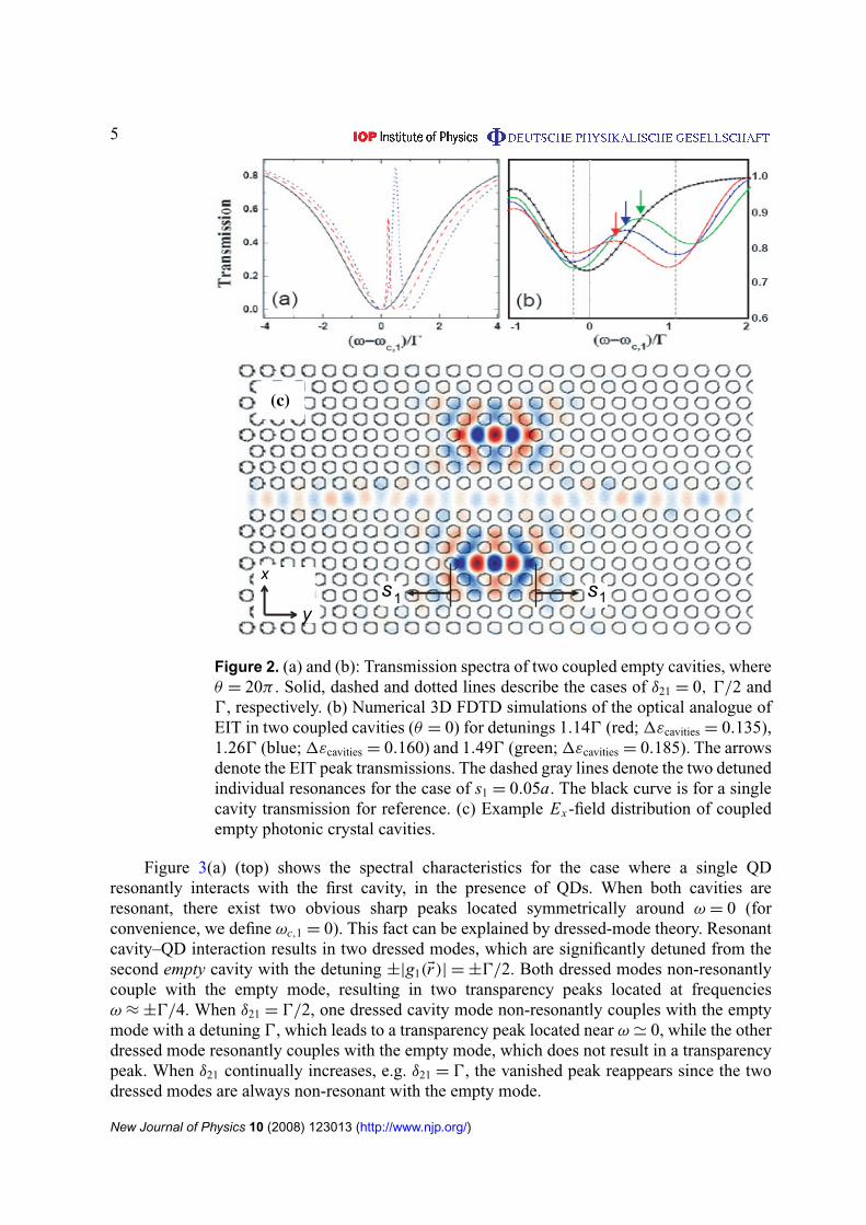
Figure 3(a) (top) shows the spectral characteristics for the case where a single QDresonantly interacts with the first cavity, in the presence of QDs. When both cavities areresonant, there exist two obvious sharp peaks located symmetrically around ω = 0 (forconvenience, we define ωc,1 = 0). This fact can be explained by dressed-mode theory. Resonantcavity–QD interaction results in two dressed modes, which are significantly detuned from thesecond empty cavity with the detuning ±|g1(Er)| = ±0/2. Both dressed modes non-resonantlycouple with the empty mode, resulting in two transparency peaks located at frequenciesω ≈ ±0/4. When δ21 = 0/2, one dressed cavity mode non-resonantly couples with the emptymode with a detuning 0, which leads to a transparency peak located near ω ' 0, while the otherdressed mode resonantly couples with the empty mode, which does not result in a transparencypeak. When δ21 continually increases, e.g. δ21 = 0, the vanished peak reappears since the twodressed modes are always non-resonant with the empty mode.
New Journal of Physics 10 (2008) 123013 (http://www.njp.org/)
6
(a)
(c) (d)
( – c,1)/
/
( – c,1)/-2 2
Tra
nsm
issi
on
(b)
21
Figure 3. (a) Transmission spectra of two coupled subsystems with one QD (top)and two QDs (bottom) where g = 0/2 and γ = γ1 = γ2 = κ0. Other conditionsare the same as in figure 2(a). (b) Spectral character of three coupled subsystemswith δ31 = 0/2 and δ1,2,3 = 0. Inset: δ31 = 0/2, δ21 = 0, δ1 = δ3 = 0, with δ2 =
0/2 (top) and δ2 = 0 (bottom). (c) and (d) Photon phase shift and delay (τsto)through two QD–cavity subsystems, where ωc(r), j = $ and g = 0.20. Inset:transmission spectrum.
Figure 3(a) (bottom) illustrates the case where both cavities resonantly interact with asingle QD each. Similar to the above analysis, we can explain the number and locations ofsharp peaks with respect to different δ21 by comparing the two pairs of dressed modes. Forexample, when δ21 = 0, the dressed modes in the first cavity are located at ±0/2, whereasthe second pair is at 0/2 and 30/2, so the transparency peaks are located at [ − 0/2, 0/2]and [0/2, 30/2], i.e. two peaks are near 0 and 0. Figure 3(b) shows the spectral character ofthree coupled cavity–QD subsystems, under various cavity–cavity and cavity–QD detunings.These transmission characteristics are helpful during experimental realization efforts to identifythe required tunings and detunings when multiple QD transitions and cavity resonances areinvolved.
3.1. Phase shift and photon storage
To further examine this coupled cavity–QD system, figure 3(c) shows the transmission phaseshift for various detunings of the input photon central frequency, where the cavity and QDtransition are resonant for both subsystems. The phase shift has a steep change as we had
New Journal of Physics 10 (2008) 123013 (http://www.njp.org/)
7
C
Lattice a1Lattice a2
QD-cavity 1
QD-cavity 2c,jr
e
g
L
R
QWP
Standing-wave coupled system on-chip
h
v
PBS1
M
PBS2 D1
D2
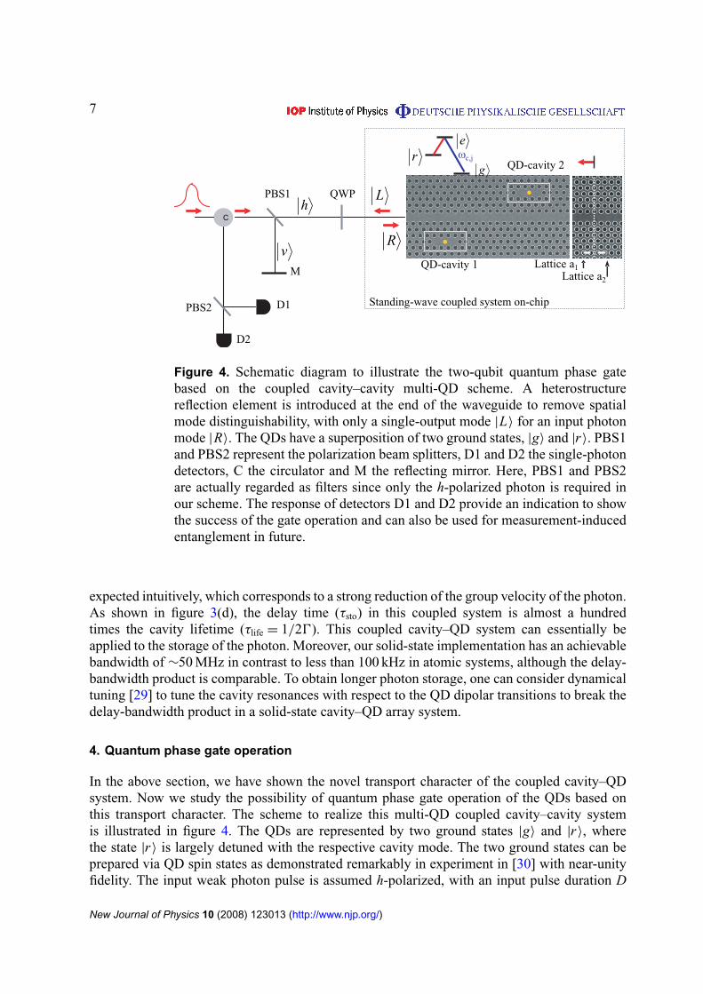
Figure 4. Schematic diagram to illustrate the two-qubit quantum phase gatebased on the coupled cavity–cavity multi-QD scheme. A heterostructurereflection element is introduced at the end of the waveguide to remove spatialmode distinguishability, with only a single-output mode |L〉 for an input photonmode |R〉. The QDs have a superposition of two ground states, |g〉 and |r〉. PBS1and PBS2 represent the polarization beam splitters, D1 and D2 the single-photondetectors, C the circulator and M the reflecting mirror. Here, PBS1 and PBS2are actually regarded as filters since only the h-polarized photon is required inour scheme. The response of detectors D1 and D2 provide an indication to showthe success of the gate operation and can also be used for measurement-inducedentanglement in future.
expected intuitively, which corresponds to a strong reduction of the group velocity of the photon.As shown in figure 3(d), the delay time (τsto) in this coupled system is almost a hundredtimes the cavity lifetime (τlife = 1/20). This coupled cavity–QD system can essentially beapplied to the storage of the photon. Moreover, our solid-state implementation has an achievablebandwidth of ∼50 MHz in contrast to less than 100 kHz in atomic systems, although the delay-bandwidth product is comparable. To obtain longer photon storage, one can consider dynamicaltuning [29] to tune the cavity resonances with respect to the QD dipolar transitions to break thedelay-bandwidth product in a solid-state cavity–QD array system.
4. Quantum phase gate operation
In the above section, we have shown the novel transport character of the coupled cavity–QDsystem. Now we study the possibility of quantum phase gate operation of the QDs based onthis transport character. The scheme to realize this multi-QD coupled cavity–cavity systemis illustrated in figure 4. The QDs are represented by two ground states |g〉 and |r〉, wherethe state |r〉 is largely detuned with the respective cavity mode. The two ground states can beprepared via QD spin states as demonstrated remarkably in experiment in [30] with near-unityfidelity. The input weak photon pulse is assumed h-polarized, with an input pulse duration D
New Journal of Physics 10 (2008) 123013 (http://www.njp.org/)
8
(e.g. 1 ns) larger than the loaded cavity lifetime for the steady-state approximation. To removethe distinguishability of the two output photon spatial modes in the waveguide (transmitted andreflected), a reflecting element is inserted at the end of the waveguide (such as a heterostructureinterface [17, 18]), as shown in figure 4. This ensures that the photon always exits in the left-propagating mode |L〉 (from a right-propagating input mode |R〉) without any entanglement withthe QD states. Alternatively, a Sagnac interferometer scheme such as introduced in [31] can alsobe implemented to remove the spatial mode distinguishability and QD–photon entanglement. Inthis single-input single-output mode scheme [32, 33], |h〉 and |v〉 represent the two polarizationstates of the input photon. We emphasize that in the below calculations we have consideredthe complete characteristics of the full system (including the end reflecting element and theresulting ‘standing wave’ due to the long photon pulse width) where we examined the final left-propagating output mode |L〉 from a right-propagating input mode |R〉 (figure 4). The reflectioninterference is included where we force b(2)
in = b(2)out (figure 1(b)) from the reflection element,
when calculating the temporal pulse delays for the different QD states.To facilitate the discussion but without loss of generality, we describe the all resonance
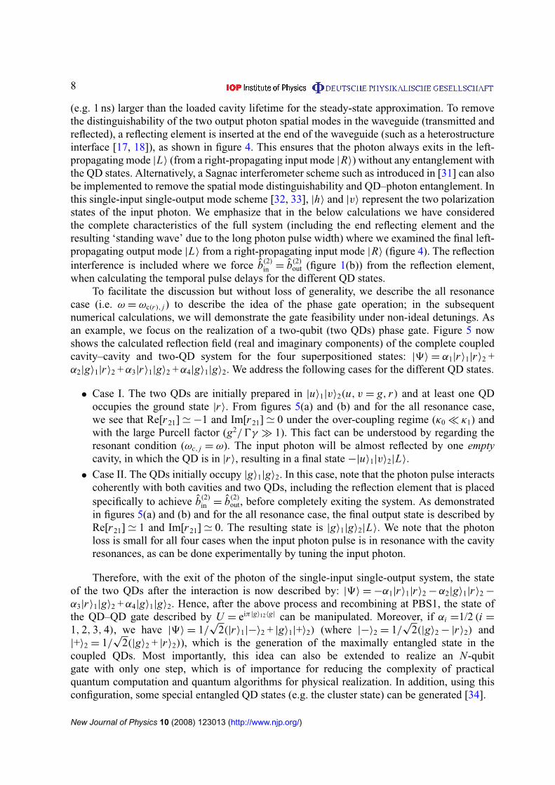
case (i.e. ω = ωc(r), j ) to describe the idea of the phase gate operation; in the subsequentnumerical calculations, we will demonstrate the gate feasibility under non-ideal detunings. Asan example, we focus on the realization of a two-qubit (two QDs) phase gate. Figure 5 nowshows the calculated reflection field (real and imaginary components) of the complete coupledcavity–cavity and two-QD system for the four superpositioned states: |9〉 = α1|r〉1|r〉2 +α2|g〉1|r〉2 + α3|r〉1|g〉2 + α4|g〉1|g〉2. We address the following cases for the different QD states.
• Case I. The two QDs are initially prepared in |u〉1|v〉2(u, v = g, r) and at least one QDoccupies the ground state |r〉. From figures 5(a) and (b) and for the all resonance case,we see that Re[r 21] ' −1 and Im[r 21] ' 0 under the over-coupling regime (κ0 � κ1) andwith the large Purcell factor (g2/0γ � 1). This fact can be understood by regarding theresonant condition (ωc, j = ω). The input photon will be almost reflected by one emptycavity, in which the QD is in |r〉, resulting in a final state −|u〉1|v〉2|L〉.
• Case II. The QDs initially occupy |g〉1|g〉2. In this case, note that the photon pulse interactscoherently with both cavities and two QDs, including the reflection element that is placedspecifically to achieve b(2)
in = b(2)out, before completely exiting the system. As demonstrated
in figures 5(a) and (b) and for the all resonance case, the final output state is described byRe[r 21] ' 1 and Im[r 21] ' 0. The resulting state is |g〉1|g〉2|L〉. We note that the photonloss is small for all four cases when the input photon pulse is in resonance with the cavityresonances, as can be done experimentally by tuning the input photon.
Therefore, with the exit of the photon of the single-input single-output system, the stateof the two QDs after the interaction is now described by: |9〉 = −α1|r〉1|r〉2 − α2|g〉1|r〉2 −
α3|r〉1|g〉2 + α4|g〉1|g〉2. Hence, after the above process and recombining at PBS1, the state ofthe QD–QD gate described by U = eiπ |g〉12〈g| can be manipulated. Moreover, if αi =1/2 (i =
1, 2, 3, 4), we have |9〉 = 1/√
2(|r〉1|−〉2 + |g〉1|+〉2) (where |−〉2 = 1/√
2(|g〉2 − |r〉2) and|+〉2 = 1/
√2(|g〉2 + |r〉2)), which is the generation of the maximally entangled state in the
coupled QDs. Most importantly, this idea can also be extended to realize an N-qubitgate with only one step, which is of importance for reducing the complexity of practicalquantum computation and quantum algorithms for physical realization. In addition, using thisconfiguration, some special entangled QD states (e.g. the cluster state) can be generated [34].
New Journal of Physics 10 (2008) 123013 (http://www.njp.org/)
9
–4 –2 0 2 4–1.0
–0.5
0.0
0.5
1.0–1.0
–0.5
0.0
0.5
1.0
c,1 /(d)
Rea
l par
tIm
agin
ary
par
t
0.0 0.2 0.4 0.6 0.8 1.0
Inte
nsi
ty (
a.u
.)
Time (ns)
initial pulse |r⟩ |g⟩
(c)
–4 –2 0 2 4–1.0
–0.5
0.0
0.5
1.0
c,1/
Imag
inar
y p
art
(b)–4 –2 0 2 4
–1.0
–0.5
0.0
0.5
1.0|g⟩
1|g⟩
2
|g⟩1|r⟩
2
|r⟩1|g⟩
2
c,1/
Rea
l par
t
(a)
|r⟩1|r⟩
2
Figure 5. Real (a) and imaginary (b) parts of the reflection coefficients for initialQD states, |r〉1|r〉2, |r〉1|g〉2, |g〉1|r〉2 and |g〉1|g〉2. Here, we assume |g1(Er)| =
|g2(Er)| = 20, δ21 = δ1 = δ2 = 0, and the propagation phase between the secondcavity and the reflection element is adjusted as θ ′
= nπ + π/2 to compensate forthe phase shift induced by the mirror reflection (ideally, π ). Other parametersare the same as in figure 2(a). (c) Shape function of the photon pulse for caseswhen the single QD is coupled (|g〉) or decoupled (|r〉) to the single cavity, andwithout the cavity. (d) Real and imaginary parts of the reflection coefficient whenthe reflection phase of the mirror deviates from ideal π with a deviation of 0.5.
We provide a few more notes on the designed coupled cavity–cavity multi-QD system.Firstly, the temporal distinguishability is small for the single cavity–QD system; in figure 5(c),we plot the shape function of the output photon pulse for cases when the QD is coupled(|g〉), decoupled (|r〉) or without the cavity, through numerical simulation of the dynamicalevolution of the system. The pulse shape function overlaps very well. Secondly, the calculatedtemporal distinguishability in the coherently coupled cavity–cavity multi-QD system is alsosmall compared with the pulse duration D. Specifically, with the parameters in figure 5(a), thephoton delays due to the coupling to the cavities are calculated as approximately τlife, 2τlife,
New Journal of Physics 10 (2008) 123013 (http://www.njp.org/)
10
Q=
10,0
00
Q=
100,
000
Q=
10,0
00
Q=
100,
000
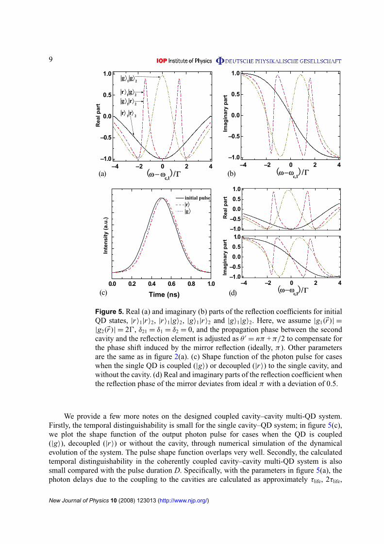
Figure 6. Gate fidelity change (δF ≡ 1 − F) (a) and photon loss P (b) of thetwo-qubit gate versus g/0. The reflecting element has 95% reflectivity. Herethe carrier frequency is assumed as $ − 2.5κ0 to avoid the EIT-like peaks oftwo coupled empty cavities, and a scattering loss of 1% is used for the shortpropagation lengths. Other parameters are the same as in figure 3(a). The shadedareas correspond to loaded cavity Q values in the range of 104 to 105.
2τlife and 4τlife in the case of the states |r〉1|r〉2, |r〉1|g〉2, |g〉1|r〉2 and |g〉1|g〉2, respectively,where the loaded cavity τlife is about 0.02 ns. The photon delay of the complete system istherefore sizably smaller than the pulse duration (of 1 ns, for example). Furthermore, this cavity-induced delay will furthermore decrease with increasing the coupling rate g, further reducingtemporal distinguishability. Of course, the size of the chip is also small (tens of microns)so that the propagation time (2S/v, where S denotes the distance between the first cavityand the reflector, and v the group velocity) in the waveguide is much smaller than the pulseduration D. Thirdly, we examine the dependence of the overall system reflection coefficient onthe phase variation from the reflection element, when deviating from the ideal π phase shift.Figure 5(d) shows the numerical results, where a slight dependence is observed when there isa phase deviation of 0.5 from π . Moreover, the phase shift from the reflection element can beexternally controlled stably, e.g. with an external and focused pump beam to thermally tune thereflection region.
New Journal of Physics 10 (2008) 123013 (http://www.njp.org/)
11
5. Gate fidelity and photon loss
To exemplify the coupled cavity system, isolated single semiconductor QDs in high-Q smallmodal volume (V) photonic crystal cavities are potential candidates, such as self-assembledInAs QDs in GaAs cavities [20]–[23], or PbS nanocrystals in silicon cavities at near 1550 nmwavelengths [35]. For the PbS nanocrystal and silicon cavity material system, we use thefollowing parameters in our calculations: γs ∼ 2 MHz, γp ∼ 1 GHz at cooled temperatures, V ∼
0.4 µm3 at 1550 nm, with a resulting single-photon coherent coupling rate of g ∼ 12.4 GHz.Loaded cavity Q values in the range of 104 and 105 are achievable experimentally, with intrinsicQ values up to 106 reported recently [18, 19].
To characterize the present gate operation, figures 6(a) and (b) present the two-qubit phasegate fidelity F and photon losses P for various g values and the parameters described above,even under non-ideal detuning conditions and the bad cavity limit. It should be noted herethat, with δ21 and δ1,2, we can know the detuning between two QDs. For example, in the caseof δ21 = 5κ0 and δ1,2 = 0, we deduce that the detuning between the two QDs is 5κ0. Basedon the above parameters, F can reach 0.99 or more, and P can be below 0.04. As shown infigure 6, for cavity–cavity detunings in the range of the intrinsic cavity decay rate, both F andP do not degrade significantly but are strongly dependent on the cavity decay rate. Likewise,with QD–cavity detuning that is comparable with the intrinsic cavity decay rate, both F andP do not change significantly but are dependent on the cavity decay rate. We note that theon-resonant (the cavity modes are resonant with the dipole transitions of the QDs) photonloss P can be larger than the non-resonant case when g is small. This can be explained byconsidering the decay of QDs. When the QDs resonantly interact with cavity modes, the decayof QDs becomes distinct, resulting in an increase of photon loss. Moreover, we note that theQD–QD detuning plays an important role in the quantum gate operations. Given the currentlarge inhomogeneous distribution of QD transitions, however, active tuning methods such asStark shifts would probably be needed to control the detuning within acceptable bounds toobtain a strong quantum gate fidelity and a low photon loss. Furthermore, we note that, withincreasing g, the photon loss P exhibits an increase before a decrease, which can be understoodby studying the photon loss when the QDs are in the state of |g〉1|g〉2. When g ' 0/2, theabsorption strength (resulting from κ0 and γ ) of the input photon by the coupled cavities reachesthe maximum.
6. Conclusion
We proposed and investigated the operation and performance of a scalable cavity–QD array on aphotonic crystal chip towards controlled quantum phase gates. The coupling among single-QDemitters and quantized cavity modes in a coherent array results in unique transmission spectra,with an optical analogue of EIT-like resonances providing potential photon manipulation. Inthe quantum phase gate operation, we note that the gate fidelity can reach 0.99 or more andthe photon loss can be below 0.04 in a realistic semiconductor system, provided the non-idealdetunings are kept within the cavity decay rates. Our study provides an approach for a chip-scaletwo-qubit gate towards a potential quantum computing network [36, 37].
Acknowledgments
We thank F Sun for helpful discussions, and acknowledge funding support from the DARPA,the New York State Office of Science, Technology and Academic Research and the NSF.
New Journal of Physics 10 (2008) 123013 (http://www.njp.org/)

12
YFX, XBZ, YLC, ZFH and GCG were also supported by Knowledge Innovation Project andInternational Partnership Project of the Chinese Academy of Sciences and by the ChinesePostdoctoral Science Foundation.
References
[1] Mabuchi H and Doherty A C 2002 Science 298 1372[2] McKeever J et al 2003 Phys. Rev. Lett. 90 133602[3] Keller M et al 2004 Nature 431 1075
McKeever J et al 2004 Nature 303 1992Kuhn A, Hennrich M and Rempe G 2002 Phys. Rev. Lett. 89 067901
[4] Volz J et al 2006 Phys. Rev. Lett. 96 030404[5] Rosenfeld W et al 2007 Phys. Rev. Lett. 98 050504[6] Smith D D et al 2004 Phys. Rev. A 69 063804[7] Xiao Y-F et al 2007 Phys. Rev. A 75 063833
Qian J, Qian Y, Feng X-L, Jin S-Q and Gong S-Q 2008 Phys. Rev. A 77 023823[8] Xu Q et al 2006 Phys. Rev. Lett. 96 123901[9] Totsuka K, Kobayashi N and Tomita M 2007 Phys. Rev. Lett. 98 213904
[10] Cirac J I, Zoller P, Kimble H J and Mabuchi H 1997 Phys. Rev. Lett. 78 3221Yao W, Liu R B and Sham L J 2005 Phys. Rev. Lett. 95 030504Serafini A, Mancini S and Bose S 2006 Phys. Rev. Lett. 96 010503
[11] Ogden C D, Irish E K and Kim M S 2008 arXiv:0804.2882[12] Hartmann M J, Brandao F G S L and Plenio M B 2006 Nat. Phys. 2 849
Hartmann M J and Plenio M B 2007 Phys. Rev. Lett. 99 103601[13] Greentree D, Tahan C, Cole J H and Hollenberg L C L 2006 Nat. Phys. 2 856
Angelakis D G, Santos M F and Bose S 2007 Phys. Rev. A 76 031805[14] Hartmann M J, Brandao F G S L and Plenio M B 2007 Phys. Rev. Lett. 99 160501[15] Hughes S 2007 Phys. Rev. Lett. 98 083603[16] Hu F M, Zhou L, Shi T and Sun C P 2007 Phys. Rev. A 76 013819[17] Tanaka Y, Upham J, Nagashima T, Sugiya T, Asano T and Noda S 2007 Nat. Mater. 6 862[18] Noda S, Fujita M and Asano T 2007 Nat. Photonics 1 449[19] Tanabe T, Notomi M, Kuramochi E, Shinya A and Taniyama H 2007 Nat. Photonics 1 49[20] Yoshie T et al 2004 Nature 432 200[21] Hennessy K et al 2007 Nature 445 896[22] Englund D et al 2007 Opt. Express 15 5550[23] Badolato A et al 2006 Science 308 1158[24] Englund D et al 2007 Nature 450 857[25] Xiao Y-F et al 2007 Appl. Phys. Lett. 91 151105[26] Waks E and Vuckovic J 2006 Phys. Rev. A 73 041803[27] Sørensen A S and Mølmer K 2003 Phys. Rev. Lett. 91 097905[28] Ghose R N 1963 Microwave Circuit Theory and Analysis (New York: McGraw-Hill)
Slater J C 1950 Microwave Circuits (New York: McGraw-Hill)Kurokawa K 1969 An Introduction to the Theory of Microwave Circuits (New York: Academic)
[29] Yanik M F, Suh W, Wang Z and Fan S 2004 Phys. Rev. Lett. 93 233903Xu Q, Dong P and Lipson M 2007 Nat. Phys. 3 406Yanik M F and Fan S 2007 Nat. Phys. 3 372
[30] Atatuer M et al 2006 Science 312 551[31] Gao J, Sun F and Wong C W 2008 Appl. Phys. Lett. 93 151108
New Journal of Physics 10 (2008) 123013 (http://www.njp.org/)
13
[32] Duan L-M, Wang B and Kimble H J 2005 Phys. Rev. A 72 032333Duan L-M and Kimble H J 2004 Phys. Rev. Lett. 92 127902Duan L-M, Kuzmich A and Kimble H J 2003 Phys. Rev. A 67 032305
[33] Lin X-M, Zhou Z-W, Ye M-Y, Xiao Y-F and Guo G-C 2006 Phys. Rev. A 73 012323[34] Cho J and Lee H-W 2005 Phys. Rev. Lett. 95 160501[35] Bose R et al 2007 Appl. Phys. Lett. 90 111117[36] Cirac J I, Zoller P, Kimble H J and Mabuchi H 1997 Phys. Rev. Lett. 78 3221[37] Serafini A, Mancini S and Bose S 2006 Phys. Rev. Lett. 96 010503
New Journal of Physics 10 (2008) 123013 (http://www.njp.org/)