Embed Size (px)
Citation preview
38 SMT Magazine • June 2012
by yash Sutariya SaTuRn elecTRonicS coRpoRaTion/SaTuRn Flex SySTeMS
summary: in 2009, author yash sutariya con-sulted Clemens lasance, a thermal management guru, who began teaching the ways of the (ther-mal) force. now, yash is curious: are brand-name thermal dielectrics on metal core printed circuit boards more effective than traditional Fr-4 PCBs with Cu-plated vias?
“Life can be much broader once you discover one simple fact: Everything around you that you call life was made up by people that were no smarter than you and you can change it.” – Steve Jobs
Like the rest of the industry, I was swept up by the high-powered marketing campaigns promoting the performance benefits of cutting-edge dielectrics for LED PCBs. Not to mention I thought it was kind of cool making a PCB from a sheet of metal. Appealing to total cost of ownership, the wave informed us that the dielectric’s reliability performance justified the higher (purchase) cost. The wave had seemingly
short-circuited that part of my brain responsible for basic physics. As a result, when the current bragged about a thermal conductivity of 2-3 W/m K, I was inhibited from realizing that this was less than 1/100 that of copper’s thermal conductivity (400 W/m K).
In 2009, I consulted a thermal management guru who began teaching me the ways of the (thermal) force. Now, like Sid the Science Kid, I just have to know: Are brand-name thermal dielectrics on metal core printed circuit boards (MCPCBs) more effective than traditional FR-4 PCBs with Cu-plated vias?
Testing the Performance of PTH and Copper Pour in Lieu of Metal Core PCBs in LED Applications
Crazy Idea: Let’s Make Circuit Boards out of FR-4!
Figure 1: McpcBs for leDs.
June 2012 • SMT Magazine 39
PCBs for LeD Thermal Management: The Basic Mechanism
The mechanism by which a thermally con-ductive PCB material works is fairly simple. The base of the LED component is soldered to a cen-ter pad of the component footprint. This cen-ter pad is not electrically connected to any of the other features. Its sole purpose is to provide a conduit for heat to be drawn away from the LED, increasing the light output as well as life of the product. MCPCBs in their simplest form consist of a circuit layer, a thermally conduc-tive dielectric layer, and a metal substrate (most commonly aluminum). Once the PCB is assem-bled it is typically mounted to a heatsink with a thermal interface material (TIM).
PCBs for LeD Thermal Management: The Basic Problems
MCPCB materials have numerous issues as-sociated with them. First and foremost is the lack of an industry specification. As our past we-binars have discussed, this results in a wide ar-ray of potential issues to the designer—primar-ily incorrect specifications that leave the end customer open to failures. Further, the MCPCB material can run up to 10 times the cost of stan-dard FR-4, eroding the full potential savings of moving from incandescent to LED lighting.
This is where the lightning bolt struck me: By drilling and plating multiple vias into the heatsink pad of the LED component footprint and using traditional FR-4 two-layer plated-through-hole technology, could I create a PCB that rivals the thermal performance of metal-clad materials that cost up to 10 times that of standard FR-4 materials?
Being a novice in thermal calculations, I called on my trusted advisor, Clemens Lasance, who is principal scientist emeritus at Philips Re-search. A good portion of his career was dedi-cated to solving the challenge of thermal man-agement electronic parts and systems. From the very beginning, Clemens was skeptical of ven-dors’ claims pertaining to thermal conductiv-ity requirements for the MCPCB in relation to thermal performance. In fact, he claimed that the MCPCB is the last element to attack in a chain that includes TIMs, heat sinks, convec-tions, and the LED itself.
His reply was quick and simple:When heat spreading is at stake, analyti-
cal solutions and approximate equations can only be used in limited cases where the design-er is dealing with one- or two-layer problems with one-sided heat transfer and one source. Fortunately, many practical cases fall into this category, such as an FR-4 board with a copper top layer or metal core PCBs with a dielectric and a metal layer. For all other situ-ations—for example when dealing with dou-ble-sided heat transfer, or multiple sources, or more than two layers, or when vias are applied, or when layers consist of more than one ma-terial, or for which the boundary conditions cannot be considered uniform—the problem becomes intractable from an approximate an-alytical point of view and we have to rely on computer codes.
It should be stressed that using analytical solutions, including the 1D series resistance network, has its main merits in getting insight, hence is second-to-none from an educational point of view. However, when accuracy is at stake in the final design stages, the recommend-ed approach for solving real-life problems is in using a 3D conduction solver.
In principle, all finite volume/finite element, etc., codes can be used that solve the 3D heat diffusion equation. In practice, only those user-friendly codes are recommended that enable a designer to get results in a couple of hours or so. Some popular CFD codes dedicated to thermal management of electronic systems (FloTHERM, 6SigmaET, Icepak) used in conduction-only mode are examples of such a code.
For a fair comparison between an FR-4 board with copper layers at both sides provided with vias and an MCPCB board there is no other way than to use a 3D conduction solver. Of course experiments also can do the job, but to explore a range of parameters such as interface materi-als, heat sinks, convection modes, a choice of vias, copper layer thickness etc., the time gained by using numerical simulations is substantial. Estimated order of magnitude: One day for nu-merical simulation; one month to prepare and perform the tests. [1, 2]
Okay, so now we know we’re on the right track. I asked Clemens to break out the Cray-
40 SMT Magazine • June 2012
ola 64-pack and draw me a picture so I could understand the concept. He did better: He cre-ated a 50,000-cell numerical model to analyze the various constructions I was discussing with him. The explanations behind these formulae and units of measurements can be found in Cle-mens’ paper “Two-Layer Heat Spreading Revis-ited,” presented at SemiTherm, March 2012, in San Jose, California [3].
We suggested comparing the following con-structions:
• MCPCB;• One-layer FR-4; and • Two-layer FR-4 with vias under LED heatsink/slug.
The basic assumptions used in the modeling were:
• LED with slug. The thermal resistance of the slug is orders of magnitude smaller than the one of the leads; hence, all power is delivered thru the slug. • The LED is not modeled except for the slug; hence, all thermal resistances are from slug to ambient.• All circular entities (slug, vias) are represented by squares with the same effective area.• The heat sink is represented by a base connected to the PCB via a TIM; the fins are represented by an effective external heat transfer coefficient.• Area allocated to a single LED is 25*25 mm.• External h: h=10 W/m2K means free convection, no heat sink. h=100 means heat sink with area extension of factor of 10. h=1,000 is forced convection and h=10,000 liquid cooling.
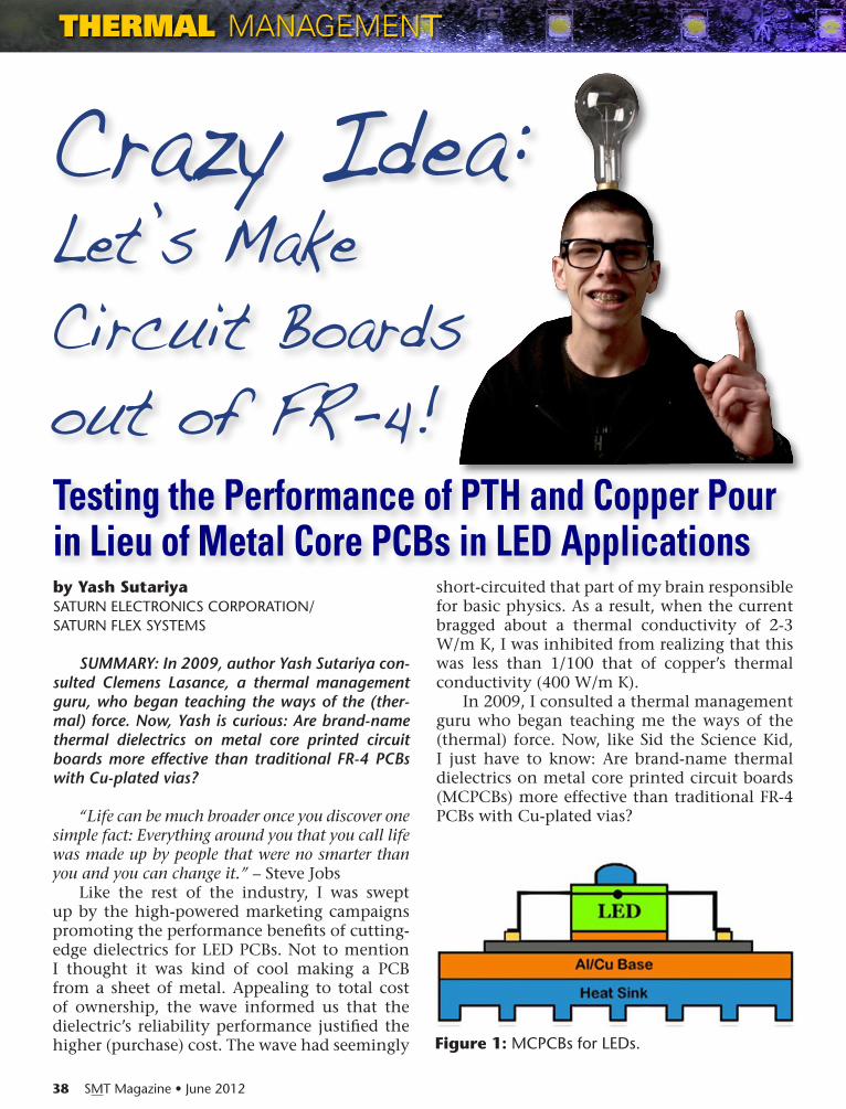
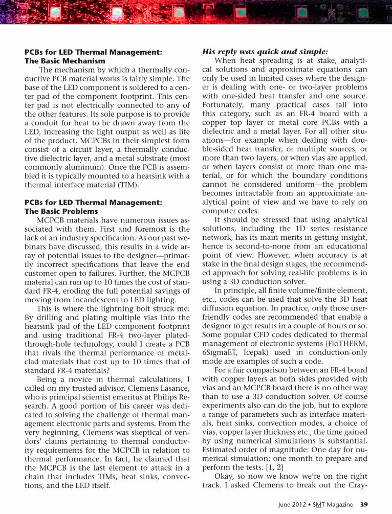
We first wanted to compare the FR-4 con-structions. In addition to the standard plated through vias, we thought to model vias that are filled with solder, as well as vias that are pure copper filled for comparison purposes.
Author’s Note: Clemens made his com-ments in regard to the following graphs:
The following graphs are based upon an anal-ysis using FloTHERM in conduction-only mode (hence not solving the Navier-Stokes equations), applying quarter symmetry to a model consisting of both layouts with the LED slug as the power source and an heat sink base of 2 mm coupled with an interface material to the PCB in question.
ConclusionAlmost no difference can be found in the
thermal performance of a standard via versus vias filled with solder or copper. This makes sense considering the very high thermal con-ductivity of copper. There is, however, a huge difference between an FR-4 board that has no vias and one that has plated through vias. Knowing this baseline data, we then plotted the thermal performance of the FR-4 boards against that of a traditional MCPCB that has a thermal resistance of approximately 0.09°C in2/W.
CRAzy IDeA: LeT’S MAKe CIRCuIT BOARDS OuT OF FR-4! continues
42 SMT Magazine • June 2012
ConclusionAlmost no difference can be found in the ther-
mal performance of a PTH FR-4 board and a MCP-CB across a wide range of convection methods (h).
For years we have been pushing the idea that plated vias having >100x the thermal con-ductivity of thermally conductive dielectrics should be a viable alternative. We now have mathematical proof of concept.
FR-4 Thermal Vias Versus Thermally Dielectric MCPCBs: An empirical Study
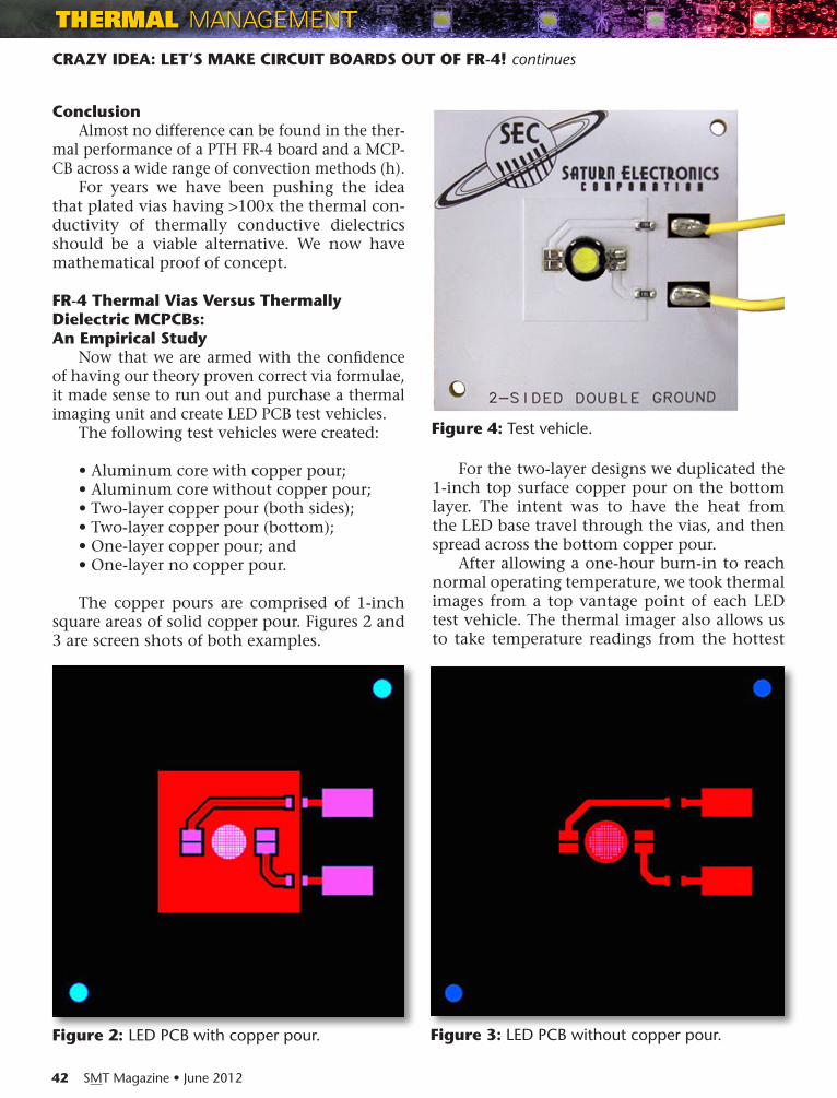
Now that we are armed with the confidence of having our theory proven correct via formulae, it made sense to run out and purchase a thermal imaging unit and create LED PCB test vehicles.
The following test vehicles were created:
• Aluminum core with copper pour;• Aluminum core without copper pour;• Two-layer copper pour (both sides);• Two-layer copper pour (bottom);• One-layer copper pour; and• One-layer no copper pour.
The copper pours are comprised of 1-inch square areas of solid copper pour. Figures 2 and 3 are screen shots of both examples.
For the two-layer designs we duplicated the 1-inch top surface copper pour on the bottom layer. The intent was to have the heat from the LED base travel through the vias, and then spread across the bottom copper pour.
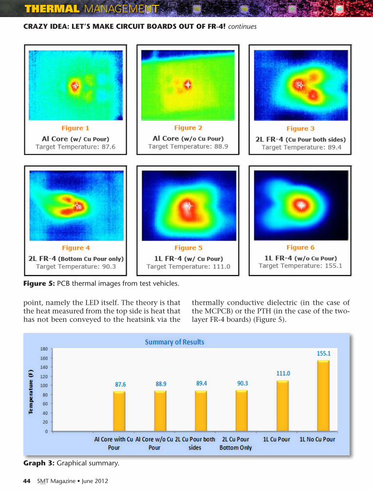
After allowing a one-hour burn-in to reach normal operating temperature, we took thermal images from a top vantage point of each LED test vehicle. The thermal imager also allows us to take temperature readings from the hottest
Figure 2: leD pcB with copper pour. Figure 3: leD pcB without copper pour.
Figure 4: Test vehicle.
CRAzy IDeA: LeT’S MAKe CIRCuIT BOARDS OuT OF FR-4! continues
44 SMT Magazine • June 2012
point, namely the LED itself. The theory is that the heat measured from the top side is heat that has not been conveyed to the heatsink via the
thermally conductive dielectric (in the case of the MCPCB) or the PTH (in the case of the two-layer FR-4 boards) (Figure 5).
Figure 5: pcb thermal images from test vehicles.
Graph 3: graphical summary.
CRAzy IDeA: LeT’S MAKe CIRCuIT BOARDS OuT OF FR-4! continues
46 SMT Magazine • June 2012
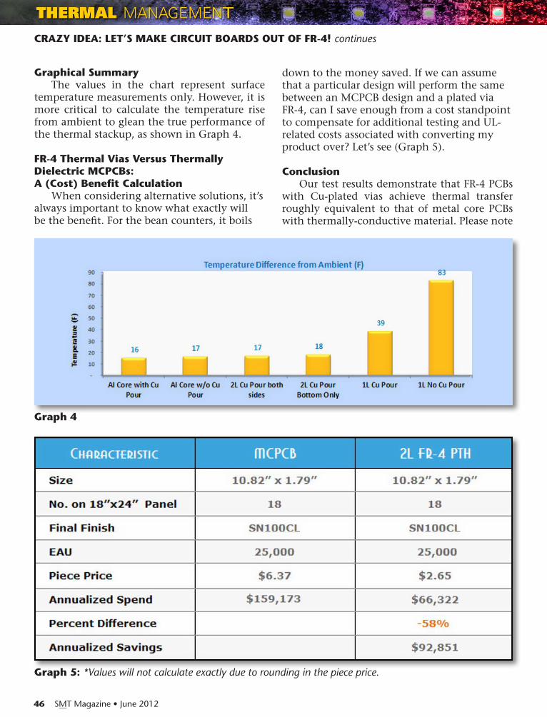
Graphical SummaryThe values in the chart represent surface
temperature measurements only. However, it is more critical to calculate the temperature rise from ambient to glean the true performance of the thermal stackup, as shown in Graph 4.
FR-4 Thermal Vias Versus Thermally Dielectric MCPCBs: A (Cost) Benefit Calculation
When considering alternative solutions, it’s always important to know what exactly will be the benefit. For the bean counters, it boils
down to the money saved. If we can assume that a particular design will perform the same between an MCPCB design and a plated via FR-4, can I save enough from a cost standpoint to compensate for additional testing and UL-related costs associated with converting my product over? Let’s see (Graph 5).
ConclusionOur test results demonstrate that FR-4 PCBs
with Cu-plated vias achieve thermal transfer roughly equivalent to that of metal core PCBs with thermally-conductive material. Please note
Graph 4
Graph 5: *Values will not calculate exactly due to rounding in the piece price.
CRAzy IDeA: LeT’S MAKe CIRCuIT BOARDS OuT OF FR-4! continues
June 2012 • SMT Magazine 47
yash Sutariya is vice president of corporate Strategy at Saturn electronics corporation (Sec) and owner/president of Saturn Flex Systems, inc. Since joining the team, Sec has successfully
navigated from a low-mix, high-volume au-tomotive supplier to a high-mix, medium- to high-volume diversified supplier. as a result of the company’s transformation, manufactur-ing capabilities now range from quick-turn prototypes to scheduled volume production while attending a broad cross-section of industries to include industrial controls, tele-communications, aerospace and power sup-ply industries.
that the results are specifically for this set of con-straints including number of vias, LED type, and choice of MCPCB. Any designer wishing to con-vert their MCPCB design to use FR-4 with plated vias should not only contact a thermal manage-ment consultant for part-specific calculations, but also perform physical tests as we have done here. Should you need, Clemens Lasance can be contacted at [email protected].
From a cost standpoint, the potential sav-ings are substantial. The raw material savings alone more than compensate for the added processing steps required to create a two-layer plated through PCB. Further, it is difficult to find a supplier that is UL certified to a particular MCPCB material; conversely, using FR-4 tech-nology allows the end user to add a great deal of competition to the supply base…as most PCB fabricators are already UL-certified to use FR-4 materials. SMT
References
1. Lasance, Clemens, “Heat spreading: not a trivial problem,” Electronics Cooling, Vol. 14, pp. 24-30, May, 2008.
2. Lasance Clemens, “How to Estimate Heat Spreading Effects in Practice,” Journal of Elec-tronics Packaging, 132, 031004, 2010.
3. Lasance Clemens, “Two-layer heat spread-ing revisited,” Proceedings, SEMITHERM, March 28, 2012, San Jose, California.
liquid crystals, the state of matter that makes possible the flat screen technology now commonly used in televisions and computers, may have new technological tricks in store. an international team of researchers led by university of wisconsin-Madi-son professor of chemical and biological Engineer-ing Juan J. de pablo reports the results of a compu-tational study that shows liquid crystals, manipu-lated at the smallest scale, can unexpectedly induce the molecules they interact with to self-organize in ways that could lead to entirely new classes of materials with new properties.
liquid crystals exhibit the order of a solid crystal but flow like a liquid. used in combination with polarizers, optical filters and electric fields, liq-uid crystals underlie the pixels that
make sharp pictures on thin computer or television displays. liquid crystal displays alone are a multi-billion dollar industry.
The new study modeled the behavior of thousands of rod-shaped liquid crystal molecules packed into nano-sized liquid droplets. it showed that the confined molecules self organize as the droplets are cooled. “at elevated temperatures, the droplets are disordered and the liquid is isotropic,” de pablo explains. “as you cool them down, they become ordered and form a liquid crystal phase. The liquid crystallinity within the droplets, surpris-ingly, induces water and other molecules at the interface of the droplets, known as surfactants,
to organize into ordered nanodo-mains. This is a behavior that was not known.”
in the absence of a liquid crystal, the molecules at the interface of the droplet adopt a homogeneous dis-tribution. in the presence of a liquid crystal, however, they form an or-dered nanostructure.
Liquid Crystal Behavior Portends new Materials
CRAzy IDeA: LeT’S MAKe CIRCuIT BOARDS OuT OF FR-4! continues