Embed Size (px)
Citation preview
CREATING EMBEDDED RADIOFREQUENCY STRUCTURES USING POLYJET
MATERIAL JETTING
Richard L. Dumene, Paul Kennedy, Christopher B. Williams1, Dennis Sweeney2, Greg Earle3
1 Design, Research, and Education for Additive Manufacturing Systems Laboratory
Department of Mechanical Engineering, Virginia Tech 2Director of Instructional Laboratories Bradley Department of Electrical and Computer
Engineering 3 Center for Space Science and Engineering Research
Bradley Department of Electrical and Computer Engineering
ABSTRACT
Embedding of integrated systems via Additive Manufacturing (AM) offers the potential to save
weight, space, and time in the production of electronics and vehicles. Of specific interest are embedded electrical systems that operate in the radiofrequency (RF) range as they have great
potential utility in communication systems and aircraft avionics including navigation. However,
systems in this frequency range pose unique manufacturing challenges such as the need to
minimize impedance discontinuities in the system. In this work, the authors explore various techniques for embedding RF structures such as antennas and filters via a multi-material jetting
AM process. Specifically, the dielectric constants and loss tangents of Vero White and Tango
Black polymers were determined to facilitate the design of RF structures with these materials. It
is shown that measurements of S-parameters of the resultant embedded RF structures approach or match the performance of non-embedded electronics.
1. INTRODUCTION
1.1. Embedding Conductive Materials into Additively Manufactured Parts
Due to its ability to provide access to the entire volume of a part throughout the build process
(Kumar, 1998), Additive Manufacturing (AM) is uniquely positioned to provide designers the
opportunity to realize multifunctional parts by embedding objects into the parts as they are fabricated. In general, embedding foreign components in an AM build process involves (a)
designing a part with a specifically designed void to accept the foreign component, (b) pausing the
print mid-build, (c) inserting the foreign object into the designed void, and (d) resuming the print
over the inserted component. Past examples of embedding objects in Additive Manufacturing processes include embedded motors via Stereo lithography (SL) (De Laurentis et al., 2002), optical
sensors via Shape Deposition Manufacturing (Li and Prinz, 2003), and shape memory alloys
(Meisel et al., 2014), LEDs and IR components in PolyJet material jetting (Willis et al., 2012).
Recent research has been focused in directly depositing conductive materials into printed layers in order to create objects that feature embedded circuitry, sensors, and/or antennae. This
capability is of great interest in integrated electronics manufacturing due to its potential to save
weight, space, and time in the production of electronic components through the embedding of
integrated systems into a printed part’s structure. This capability is also beneficial to AM in
1769
general, as it provides an opportunity to integrate the manufacturing of multi-material complex
systems into a singular manufacturing process.
The majority of effort in printing components with embedded circuitry has focused in the
integration of Direct Write (DW) and AM technologies. DW is a set of technologies that enable
selective deposition of material onto a substrate, and include extrusion, droplet jetting, aerosol
jetting, laser transfer, and tip transfer technologies (Hon et al., 2008). The integration of DW and AM technologies the creation of complex and conformal electronics (interconnects, sensors, etc.)
that are structurally integrated into a manufactured part. One of the first examples of integrating
the two technologies was demonstrated by a research team at the University of Texas El Paso
(UTEP); the hybrid process worked by first pausing the SL build, using a direct write device to extrude a conductive paste onto the layer in the pattern of the desired circuit, and then resuming
the build to embed the printed circuit (Lopes et al., 2005; Medina et al., 2005; Palmer, 2005).
Additional examples of hybridizing DW and AM to create parts with embedded circuits have also
been demonstrated in Ultrasonic Consolidation (Robinson et al., 2006), screw extrusion (Malone et al., 2008), fused filament extrusion (Breyfogle and Cormier, 2013), polymer powder bed fusion
(Folgar et al., 2014), and multi-material jetting processes (Perez and Williams, 2014a).
Following an in-depth analysis of the integration of DW and AM technologies, it was observed that the direct application of dissimilar materials is challenging as it is hampered by (i) identifying
DW materials and processes that are compatible with AM infrastructure, throughput and
resolution, (ii) temperature processing requirements, and (iii) interactions between the two
materials (Perez and Williams, 2014b). These physical limitations have resulted in embedded circuits that have fairly high resistivity, which limits their application.
Due to these challenges, many are investigating other means of incorporating conductive
materials into printed layers. Specifically, instead of directly writing conductive materials onto a printed substrate, researchers are investigating the embedding of conductive copper wire and direct
placement of pre-fabricated sensors and integrated circuits. Early efforts in this approach were
focused in embedding wires and sensors into machined pockets in Ultrasonic Consolidation builds
(Siggard et al., 2006). More recent research from the UTEP group has demonstrated the use of an ultrasonic wire embedding device to directly embed/write copper wire into polycarbonate printed
via Extrusion AM (Kim et al., 2015). This system has enabled the creation of complex systems
such as a CubeSat featuring embedded interconnects that are laser-welded to surface mount
devices (Espalin et al., 2014). Copper wire and coper mesh has also been embedded into polycarbonate material to create capacitive sensors (Shemelya et al., 2015).
1.2. Fabricating Radio Frequency Structures via Additively Manufacturing
As noted above, most of the research in embedding electronics into AM components has
focused on direct printing sensors and interconnects. There is emerging interest in fabricated
embedded electrical systems that operate in the radiofrequency (RF) range, as they have great utility in communication systems and aircraft avionics, such as radar. Highly integrated systems
with limited space such as CubeSATs and small UAVs would significantly benefit if antennas and
receivers were able to be embedded in the structure of the CubeSAT. Similarly, the design of 3D
printed GHz antennas could one day facilitate a 3D printed cell phone. Another possibility is to embed radar hardware in the wings of UAVs. In order to realize these possibilities, certain
1770
challenges in the manufacture of these systems must be overcome including the need to minimize
impedance discontinuities in the system and the need to characterize the electromagnetic properties
of materials used in AM.
The University of Texas at El Paso research groups has conducted research in the area of
embedding RF structures into AM parts. Deffenbaugh used stereo lithography (SL) and fused
deposition modeling (FDM) to build RF structures (2014). Specifically, SL was used to build micro strip transmission lines, a strip line, and a suspended micro strip structure. FDM methods
were used to build a curve inverted-F antenna. This research demonstrated that RF structures can
be constructed using additive manufacturing technologies. Deffenbaugh identified two key
obstacles for process development, (i) the FDM system has a relatively low-resolution and (ii) SL is limited in its embedding abilities as it relies on curing resin in a vat. Similarly, a patch antenna
was created by Robinson and coauthors by using a hybridized DW and Ultrasonic Consolidation
system (2006).
1.3. Context
The goal of this work is to explore the use of the PolyJet material jetting process as a means of
fabricating printed parts with embedded RF structures. The primary objects are to demonstrate
the feasibility of embedding RF structures in this process, and to assess their resultant quality (via
S-parameter measurements). As discussed in Section 2, the PolyJet process has both unique advantages (e.g., the ability to fabricate multi-material components that have tailored stiffness and
flexibility) and unique disadvantages (e.g., the low heat deflection temperature of the printed
polymers), that make this a challenging problem. Through the developed embedding technique,
the authors successfully fabricated five different RF structures that are embedded in three different PolyJet material systems. Details of the design of these structures are presented in Section 3, along
with a description the experimental methods employed to analytically predict and experimentally
measure their performance. The results of the fabrication process and the measurements of the RF
structures’ performance are presented in Section 4. Closure is offered in Section 5.
2. EMBEDDING RF STRUCTURES IN POLYJET MATERIALS
PolyJet is a material jetting AM process that uses drop-on-demand inkjet printing to selectively
deposit droplets of photopolymer directly onto a build platform. Once a layer of droplets is
deposited via inkjet print heads, a roller evens out the layer surface, and two UV lights (one leading
and one trailing) pass over the printed layer multiple times to fully cure the photopolymer. As several inkjet print heads with separate material sources can be installed into the printing block,
multiple materials can be deposited in a single layer, thus enabling the creation of graded materials.
For example, the use of Vero White Plus (a stiff polymer) and Tango Black Plus (a flexible,
elastomeric material) enables a designer to create products with graded stiffness. A sacrificial support material is also deposited during a build to support the fabrication of complex geometries.
This sacrificial material is removed using a compressed water jet in a post-processing step.
The PolyJet process creates new layers by direct material addition (Williams et al., 2011), which is well suited for component embedding. The lack of a recoating step, wherein raw material
is added in bulk in powder or resin form, eliminates concerns of disturbing the previously printed
layer typically found in embedding processes. The authors have demonstrated the use of PolyJet
1771
to realize products with embedded monofilament (Stiltner et al., 2011), shape memory alloy
actuators (Meisel et al., 2014), direct write circuits (Perez et al., 2014a), and other photopolymer
materials (e.g., quantum dot composites resins (Elliott et al., 2013)). Although different in form and function, each of these components was embedded into a part during printing by following a
generalized four-step process: (i) designing a cavity for the component, (ii) pausing the build at
the topmost layer of the cavity, (iii) inserting the component and (iv) resuming the build. One of
the key aspects of the embedding process for PolyJet is the need to remove support material from the cavities in the printed part in order to properly place any desired embedded components. In
addition, since the print head assembly block passes over the printed part at a clearance of only
100 µm, embedded components cannot protrude from the previously deposited layer, or damage
to the printing nozzles could occur.
The authors have previously embedded electronic components in PolyJet builds by inserting a
pneumatically-controlled extrusion printer into the PolyJet system, and selectively depositing a
conductive paste onto a printed layer (Perez et al., 201b). While this was successfully used to deposit interconnects and to fabricate a strain gauge, the low heat deflection temperature of the
printed photopolymer (54°C) prevented the application of the recommended heat treatment for the
deposited material. Thus, the deposited conductive traces had high resistivity, and prevented the
creation of electronic structures that required significant current.
To address this limitation, the authors look to the direct embedding of copper materials to
create electronic components, as done previously in Extrusion AM (Section 1.1). However,
instead of embedding copper wire or mesh (Espalin et al., 2014; Shemelya et al., 2015), the authors look to the use of copper foil adhesive tape as a means of creating RF structures. Copper tape is
conventionally used for creating low-profile conductive traces, antenna fabrication, and for RF-
shielding. It is sufficiently conductive for RF applications, and its width enables the creation of
designed filters and antennae structures by precision cutting (via blade or laser cutter) into a designed shape. The adhesive backing also allows for efficient application and anchoring into a
pre-designed cavity. This approach proved to be much faster and cheaper than selectively
extruding nano-silver conductive paste.
To facilitate the embedding of copper tape, the designed part must be altered to feature a
sufficient cavity to accept the tape in order to prevent collision of the objet with the print heads.
When paused, support material is removed using precision tools; the exposed surface of the part
is then cleaned using 99% isopropyl alcohol to remove residual support material and prepare the surface for adhesives. Additionally, access holes for tooling access into the part must be designed
and produced. The design of access holes is particularly challenging for ensuring access for the
soldering iron, which is used to attach connectors to the embedded RF structures. The soldering
iron must not be permitted to touch the material as the melting point of the cured photopolymers is significantly lower than that of solder (SAC350). The most successful approach required the
use of wide, shallow holes to facilitate easy access with a soldering iron. After the connectors are
affixed to the conductors, any access windows or ports can be filled with epoxy or photopolymer
and then cured via UV.
3. EXPERIMENTAL METHODS
1772
The fabricated RF structure, and the experimental methods used to measure them, are presented
in this section. All samples were printed using a Stratasys Connex 350 PolyJet AM system and
were made from either Vero White Plus (VW), Tango Black Plus (TB), or Shore95, a composite of the VW and TB materials.
3.1. Characterizing Dielectric Constants
The dielectric constant of the substrate material determines the dimensions of the transmission
line structures. Initial estimates of the dielectric constant were produced based on the impedance of early attempts at building transmission lines. To more accurately determine the dielectric
constant, capacitor test fixtures were constructed. Capacitor structures were chosen because
capacitors are well understood and their capacitance is a clear function of dielectric constant. The
procedure for determining the dielectric constant first involved printing 1” square capacitors from the 3D printed materials (VW, TB, and Shore95) to serve as substrates from copper tape, which
served as the plates. Once the embedding and printing was complete, the authors measured the
capacitance and then calculated the dielectric constant.
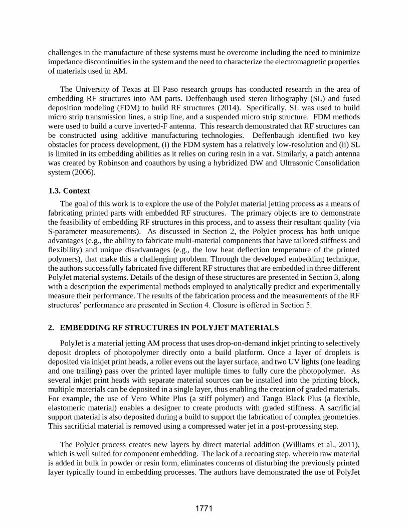
Figure 1. Q-meter and equivalent circuit schematic.
The capacitance measurements were obtained via a 4342A Hewlett Packard Q-meter (Figure
1). The Q-meter circuit is an inductor in parallel with a variable capacitor. The variable capacitor
was adjusted until the circuit reached resonance. Then, the capacitor under test was placed in parallel with the variable capacitor. The variable capacitor was again adjusted to tune the circuit.
The difference between the first and second values of the variable capacitor was equivalent to the
capacitance of the capacitor under test. This capacitance value, along with the dimensions of the
capacitor, was used to calculated the dielectric constant, εr.
3.2. Design and Fabrication of RF Structures
Following the process outlined in Section 2, several embedded RF structures were made using
VW, TB, and Shore95 materials. The authors chose well understood structures so that well known
analytical models could be used to design the dimensions for these structures, and so that
commercial simulation software could be used to verify that the fabricated structures were performing appropriately (Section 3.4).
Coaxial cable: The first embed consisted a simple copper clad coaxial cable. This sample was a 0.047 inch copper cladded coaxial cable embedded in an 8 inch (20cm) strip of Vero
White photopolymer. For simplicity, this part was embedded without connectors using a
simple U channel. After embedding the cable, it was secured to the structure using Super
1773
Glue before resuming the print. This prevented the part from rising off of the build platform
and potentially damaging the print heads. After successfully embedding the cable, SMA
connectors were soldered to the cable.
Micro strip transmission lines: A micro strip was made from VW, and was designed to have
an impedance of 50 ohms. Copper tape of different widths was affixed to a substrate 0.1” in
height. The connectors were then soldered to the copper tape. Two micro strip transmission lines were created; one mounted on the surface of the printed substrate, and one completely
encapsulated by the printed material.
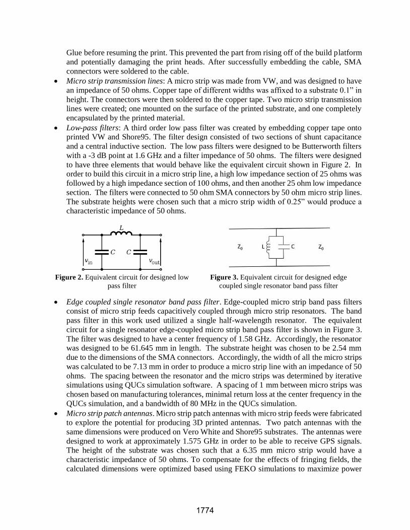
Low-pass filters: A third order low pass filter was created by embedding copper tape onto printed VW and Shore95. The filter design consisted of two sections of shunt capacitance
and a central inductive section. The low pass filters were designed to be Butterworth filters
with a -3 dB point at 1.6 GHz and a filter impedance of 50 ohms. The filters were designed
to have three elements that would behave like the equivalent circuit shown in Figure 2. In order to build this circuit in a micro strip line, a high low impedance section of 25 ohms was
followed by a high impedance section of 100 ohms, and then another 25 ohm low impedance
section. The filters were connected to 50 ohm SMA connectors by 50 ohm micro strip lines.
The substrate heights were chosen such that a micro strip width of 0.25” would produce a characteristic impedance of 50 ohms.
Figure 2. Equivalent circuit for designed low
pass filter
Figure 3. Equivalent circuit for designed edge
coupled single resonator band pass filter
Edge coupled single resonator band pass filter. Edge-coupled micro strip band pass filters consist of micro strip feeds capacitively coupled through micro strip resonators. The band
pass filter in this work used utilized a single half-wavelength resonator. The equivalent
circuit for a single resonator edge-coupled micro strip band pass filter is shown in Figure 3.
The filter was designed to have a center frequency of 1.58 GHz. Accordingly, the resonator was designed to be 61.645 mm in length. The substrate height was chosen to be 2.54 mm
due to the dimensions of the SMA connectors. Accordingly, the width of all the micro strips
was calculated to be 7.13 mm in order to produce a micro strip line with an impedance of 50
ohms. The spacing between the resonator and the micro strips was determined by iterative simulations using QUCs simulation software. A spacing of 1 mm between micro strips was
chosen based on manufacturing tolerances, minimal return loss at the center frequency in the
QUCs simulation, and a bandwidth of 80 MHz in the QUCs simulation.
Micro strip patch antennas. Micro strip patch antennas with micro strip feeds were fabricated to explore the potential for producing 3D printed antennas. Two patch antennas with the
same dimensions were produced on Vero White and Shore95 substrates. The antennas were
designed to work at approximately 1.575 GHz in order to be able to receive GPS signals. The height of the substrate was chosen such that a 6.35 mm micro strip would have a
characteristic impedance of 50 ohms. To compensate for the effects of fringing fields, the
calculated dimensions were optimized based using FEKO simulations to maximize power
1774
output at 1.575 GHz. Given the widespread use of GPS in cell phones, UAVs, and CubeSATs
building a 3D printed GPS antenna advances the progress towards developing a fully
integrated 3D printed UAV or cell phone.
3.3. Characterizing RF Performance
A Tektronix 1502 Time Domain Reflectometer (TDR) Cable Tester was used to determine the
location of discontinuities and impedance changes within the fabricated structures. The TDR
sends an impulse down the device and records the time delay before the reflection reaches the
TDR. It then calculates the reflection coefficient as a function of length based on this time delay. Any deviations in the reflection coefficient signifies an impedance mismatch or discontinuity
within the transmission line. Since the TDR provides this information as a function of length, the
discontinuity can be easily located on the device under test. This device was used to determine the
quality of solder joints between the SMA connectors and the transmission lines, and also enabled the comparison and visualization of the impedance of multiple sections of an embedded
transmission line.
The performance of the radiofrequency structures was characterized by a two port measurement of the scattering (S-parameter) matrix using 2 port S-parameter measurements on a
Rohde & Schwarz ZVL13 Network Analyzer. The network analyzer was designed to work from
9 kHz to 13.5 GHz. The impedance, as a function of frequency, was also calculated from the
reflection coefficient, S11. The devices were characterized over a frequency range from 0.1 to 10 GHz. In order to ensure the accuracy of the measurements, the network analyzer was calibrated
before each measurement session using a ZV-Z135 Rohde & Schwarz calibration kit.
When analyzing the S-parameter measurements, an S21 measurement of 0 dB represented a perfect transmission line. Similarly, an S11 measurement of 0 dB represented a perfect open or
short. When analyzing filters, the cutoff frequency, or -3 dB point, occurs when the S21 parameter
is 3 dB below its maximum point. This cutoff frequency is significant as it represent where half
of the maximum power is transmitted.
3.4. Simulation of Fabricated RF Structures
The authors employed two separate simulation software packages to verify that the designed
RF structures were performing as expected. First, Qucs (Quite Universal Circuit Simulator) was
used to build schematic representations of the samples and predict their S-parameter values with
changes in frequency. Qucs is a circuit simulator similar to Agilent ADS in that it can simulate micro strip and strip line circuits, including filter geometries, in the GHz range. Major advantages
of Qucs included the short simulation time and the short time required to construct schematics for
simple structures.
Qucs, however, does not support producing 3D models of the structures nor simulation of
antenna designs. As two of the major goals of this project were to utilize the complex geometries
possible with additive manufacturing and to design antennas for embedding, another software
platform was needed. FEKO, an EM Simulation Software, was used to build 3D representations of the structures, and then to simulate the S-parameters, impedances, and far fields of the various
structures as a function of frequency. While simulating structures in FEKO is considerably more
1775
time intensive, the simulation results in FEKO were more accurate than the results from Qucs.
The difference in performance became more significant as frequency increased. The deviation in
performance of these two modelling tools can be seen in the discussion of the Vero White low-pass micro strip filter specimen (Section 4.4). Ultimately, both tools showed potential as tools in
the design of 3D printed RF structures.
4. RESULTS AND DISCUSSION
4.1. Dielectric Constants of PolyJet Material
The average dielectric constants and 95% confidence intervals for VW, TB, and Shore95 (a
composite of VW and TB) materials are shown in Table 1. The interval for VW and Shore95 are small, but the range for TB is wider. While this range could be due to variations in the printed
material, it is likely a result of challenges in measuring the capacitance of the TB capacitors. TB
is a flexible material, so the capacitors would bend, causing the copper tape to peel off of the TB
dielectric. Table 1. Dielectric Constants and 95% Confidence Intervals
Material Average Dielectric Constant 95% Confidence Interval
Vero White 2.9521 [2.9082, 2.9960]
Tango Black 2.8161 [2.4563, 3.1758]
Shore95 3.1936 [3.1245, 3.2628]
Initially, the empirical results of the structures did not match expectations based on simulations
of the structures. This discrepancy was due to the notable loss tangent of the VW, which was used
in most of the initial structures. A loss tangent of 0.0285 was calculated for the VW substrate by
fitting the simulated curve to the empirical results. For comparison, the loss tangents of VW and
other common materials are shown in Table 2. VW is far more lossy than industry standard FR-4, and more closely resembles the large loss of wood. This large loss tangent suggests there are
limitations to the utility of Vero White substrates in the construction of transmission lines.
However, the potential exists to utilize the complex geometries possible with AM to create VW
structures with less loss. Table 2. Common Materials and Dielectric Characteristics
Material Relative Permittivity Loss Tangent
Fused quartz 3.8 0.00006 @ 3 GHz
Teflon (PTFE) 2.0 - 2.1 0.00028 @ 3 GHz
FR-4 -high resin 4.2 0.008 @ 3 GHz
ABS (plastic), Molded 2.0 - 3.5 0.00500 - 0.0190
Vero White 2.97 0.0285 @ 1.5 GHz
1776
Wood 1.2 - 2.1 0.03 @ 3 GHz
4.2. Coaxial Cable
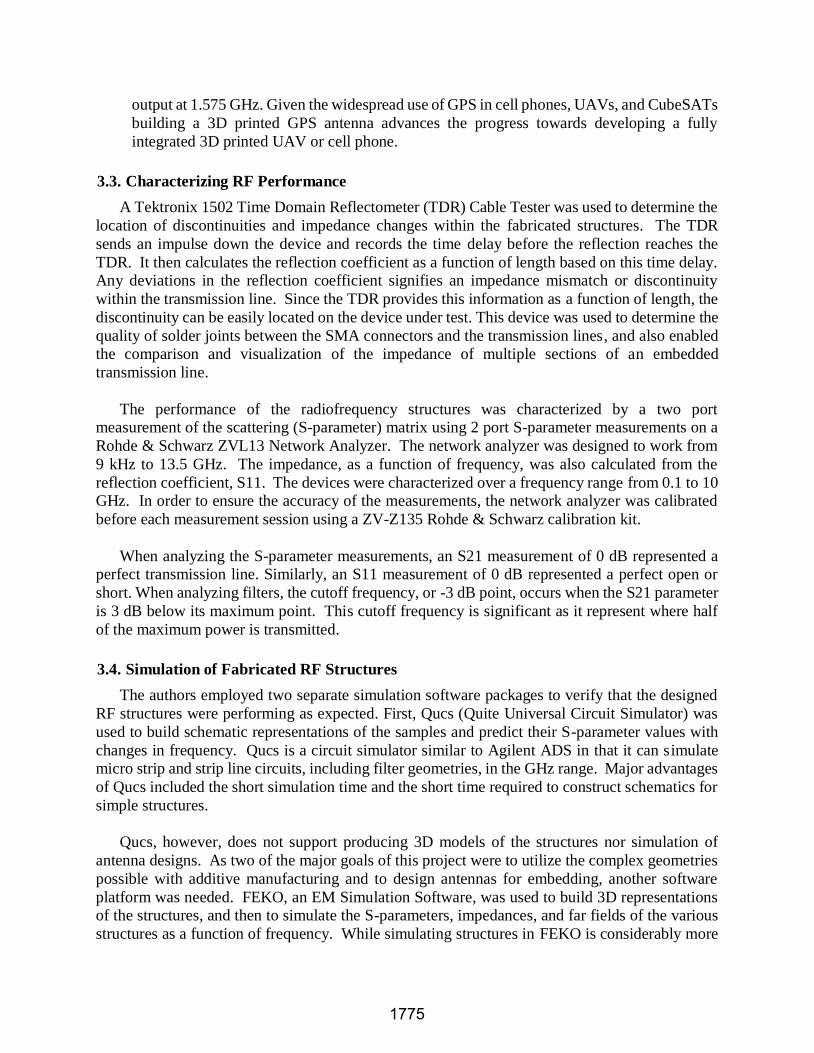
As presented in Section 3.2, the first embedded object was a copper cladded coaxial cable
embedded into a strip of VW (Figure 4).
Figure 4. An early embedded coaxial cable demonstrating embedding capabilities.
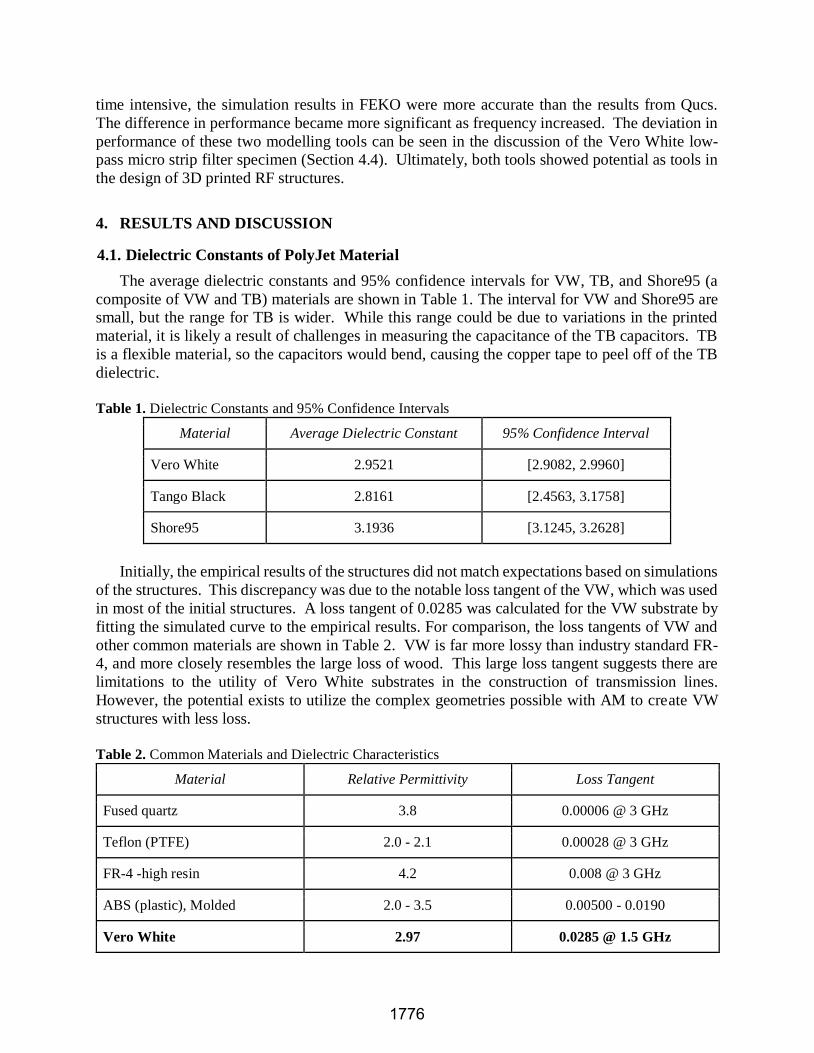
Following the soldering of SMA connectors, a network analyzer was used to evaluate the
system. This system performed well into the GHz range as expected. It can be seen in Figure 6 that
the S21 measurement was almost 0 dB across the entire spectrum indicating a near perfect
transmission line. Thus, GHz structures can be created using simple embedding techniques and widely available materials such as coaxial cables. Using coaxial cable isolated the RF performance
of the TEM structure from the tolerances and errors inherent in the printing process. This type of
system would be most useful for connecting application specific sections, such as filters and
antennas, when the transmission path may have to move in three dimensions or outside of a printed part.
Figure 5. Parameter measurements from the embedded coaxial cable. The S21 of almost 0 dB
indicates an almost ideal transmission line.
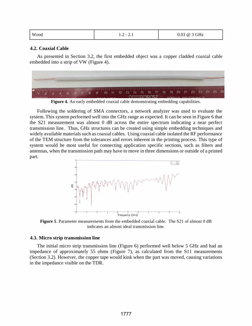
4.3. Micro strip transmission line
The initial micro strip transmission line (Figure 6) performed well below 5 GHz and had an impedance of approximately 55 ohms (Figure 7), as calculated from the S11 measurements
(Section 3.2). However, the copper tape would kink when the part was moved, causing variations
in the impedance visible on the TDR.
1777
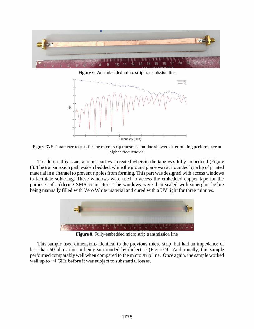
Figure 6. An embedded micro strip transmission line
Figure 7. S-Parameter results for the micro strip transmission line showed deteriorating performance at
higher frequencies.
To address this issue, another part was created wherein the tape was fully embedded (Figure
8). The transmission path was embedded, while the ground plane was surrounded by a lip of printed
material in a channel to prevent ripples from forming. This part was designed with access windows to facilitate soldering. These windows were used to access the embedded copper tape for the
purposes of soldering SMA connectors. The windows were then sealed with superglue before
being manually filled with Vero White material and cured with a UV light for three minutes.
Figure 8. Fully-embedded micro strip transmission line
This sample used dimensions identical to the previous micro strip, but had an impedance of
less than 50 ohms due to being surrounded by dielectric (Figure 9). Additionally, this sample performed comparably well when compared to the micro strip line. Once again, the sample worked
well up to ~4 GHz before it was subject to substantial losses.
1778
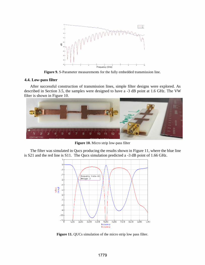
Figure 9. S-Parameter measurements for the fully embedded transmission line.
4.4. Low-pass filter
After successful construction of transmission lines, simple filter designs were explored. As
described in Section 3.5, the samples were designed to have a -3 dB point at 1.6 GHz. The VW
filter is shown in Figure 10.
Figure 10. Micro strip low-pass filter
The filter was simulated in Qucs producing the results shown in Figure 11, where the blue line
is S21 and the red line is S11. The Qucs simulation predicted a -3 dB point of 1.66 GHz.
Figure 11. QUCs simulation of the micro strip low pass filter.
1779
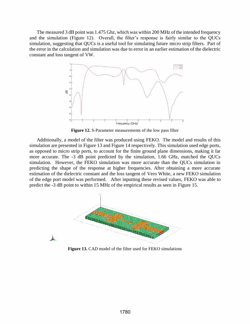
The measured 3 dB point was 1.475 Ghz, which was within 200 MHz of the intended frequency
and the simulation (Figure 12). Overall, the filter’s response is fairly similar to the QUCs
simulation, suggesting that QUCs is a useful tool for simulating future micro strip filters. Part of the error in the calculation and simulation was due to error in an earlier estimation of the dielectric
constant and loss tangent of VW.
Figure 12. S-Parameter measurements of the low pass filter
Additionally, a model of the filter was produced using FEKO. The model and results of this simulation are presented in Figure 13 and Figure 14 respectively. This simulation used edge ports,
as opposed to micro strip ports, to account for the finite ground plane dimensions, making it far
more accurate. The -3 dB point predicted by the simulation, 1.66 GHz, matched the QUCs
simulation. However, the FEKO simulation was more accurate than the QUCs simulation in predicting the shape of the response at higher frequencies. After obtaining a more accurate
estimation of the dielectric constant and the loss tangent of Vero White, a new FEKO simulation
of the edge port model was performed. After inputting these revised values, FEKO was able to
predict the -3 dB point to within 15 MHz of the empirical results as seen in Figure 15.
Figure 13. CAD model of the filter used for FEKO simulations
1780
Figure 14. S-Parameters produced from the FEKO simulation
Figure 15. Zoomed view of FEKO results showing accuracy of the simulation values
In addition to creating a filter using VW, a filter made on Shore95 material was also fabricated
(Figure 16). As with the VW sample, the filter was designed to have a -3 dB point at 1.6 GHz.
Empirical results showed a -3 dB point at 1.565 GHz. Despite being the first attempt at a Shure95 structure, the -3 dB point was only 35 MHz from the design value, a 2.19% error. This sample
illustrates the capability of AM technologies to produce useful RF structures from a variety of
materials with known electrical properties.
1781
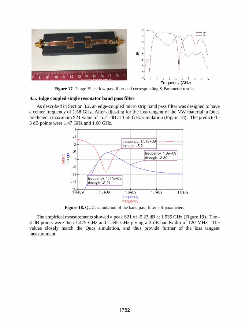
Figure 17. Tango Black low pass filter and corresponding S-Parameter results
4.5. Edge coupled single resonator band pass filter
As described in Section 3.2, an edge-coupled micro strip band pass filter was designed to have a center frequency of 1.58 GHz. After adjusting for the loss tangent of the VW material, a Qucs
predicted a maximum S21 value of -5.21 dB at 1.58 GHz simulation (Figure 18). The predicted -
3 dB points were 1.47 GHz and 1.60 GHz.
Figure 18. QUCs simulation of the band pass filter’s S-parameters
The empirical measurements showed a peak S21 of -5.23 dB at 1.535 GHz (Figure 19). The -
3 dB points were then 1.475 GHz and 1.595 GHz giving a 3 dB bandwidth of 120 MHz. The
values closely match the Qucs simulation, and thus provide further of the loss tangent
measurement.
1782
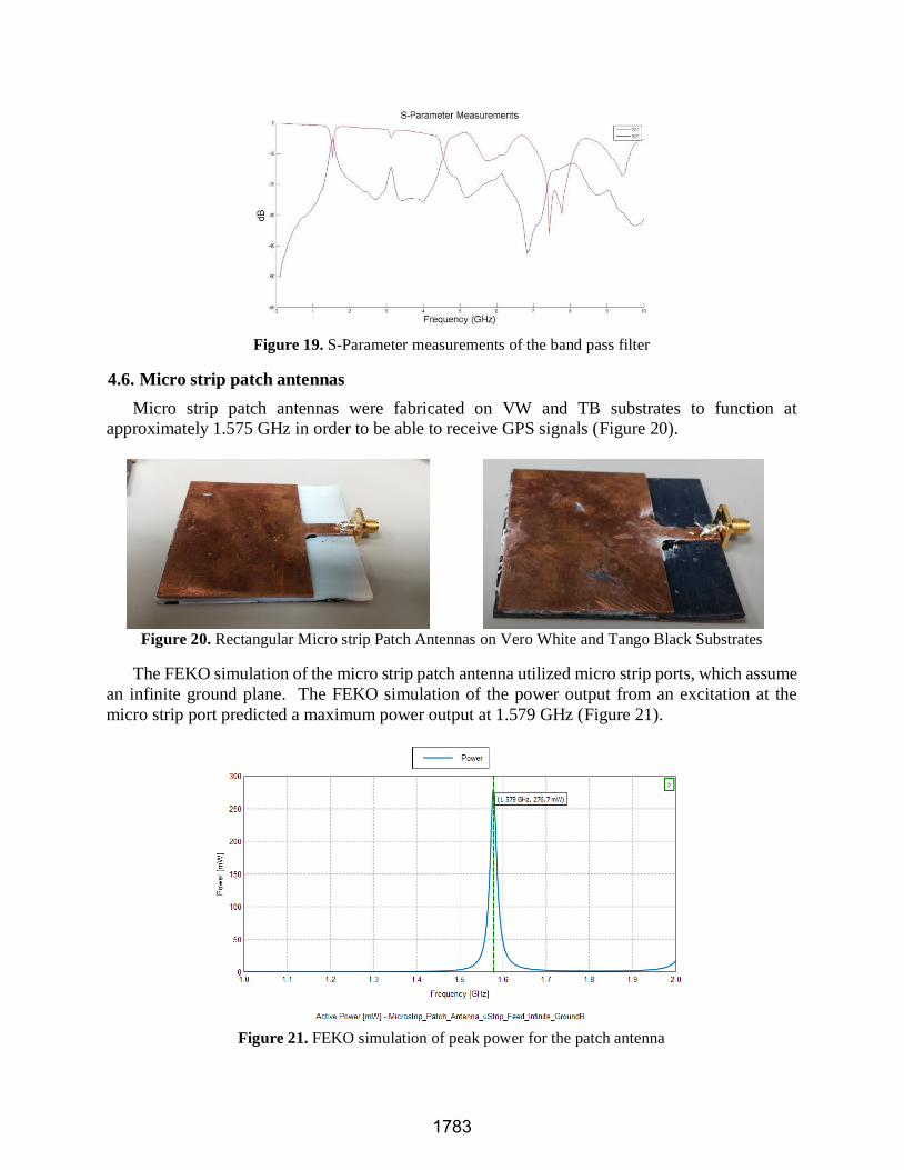
Figure 19. S-Parameter measurements of the band pass filter
4.6. Micro strip patch antennas
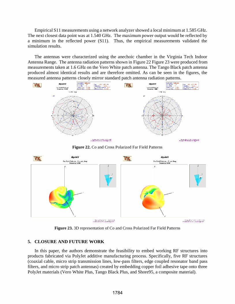
Micro strip patch antennas were fabricated on VW and TB substrates to function at approximately 1.575 GHz in order to be able to receive GPS signals (Figure 20).
Figure 20. Rectangular Micro strip Patch Antennas on Vero White and Tango Black Substrates
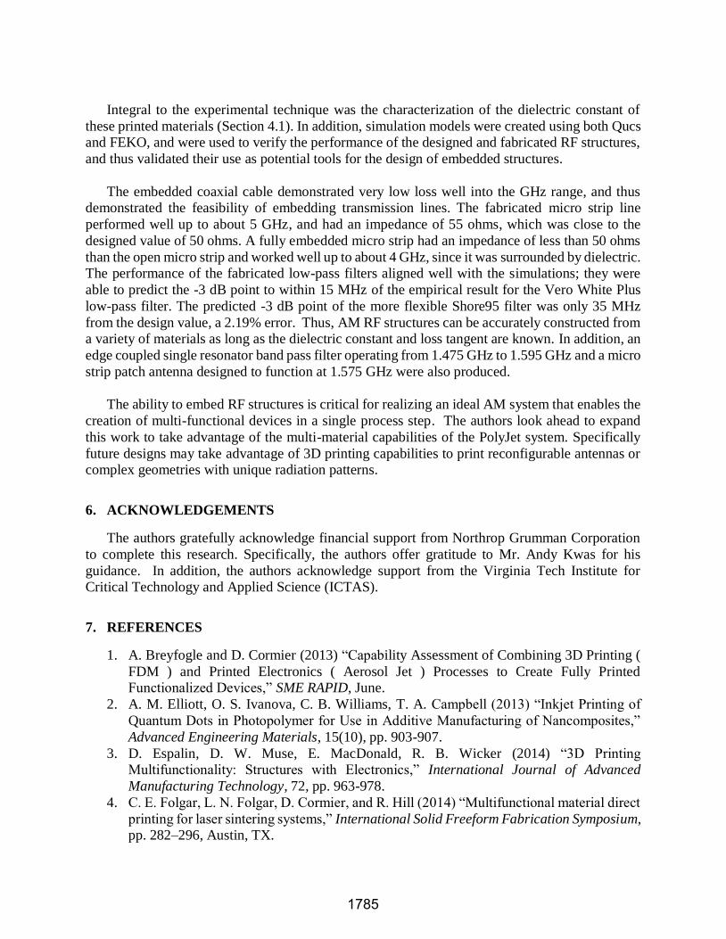
The FEKO simulation of the micro strip patch antenna utilized micro strip ports, which assume
an infinite ground plane. The FEKO simulation of the power output from an excitation at the
micro strip port predicted a maximum power output at 1.579 GHz (Figure 21).
Figure 21. FEKO simulation of peak power for the patch antenna
1783
Empirical S11 measurements using a network analyzer showed a local minimum at 1.585 GHz.
The next closest data point was at 1.540 GHz. The maximum power output would be reflected by
a minimum in the reflected power (S11). Thus, the empirical measurements validated the simulation results.
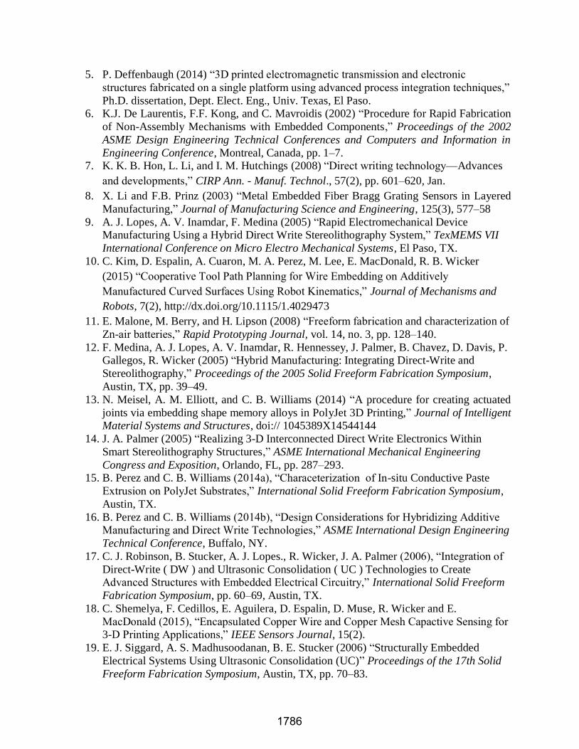
The antennas were characterized using the anechoic chamber in the Virginia Tech Indoor
Antenna Range. The antenna radiation patterns shown in Figure 22 Figure 23 were produced from measurements taken at 1.6 GHz on the Vero White patch antenna. The Tango Black patch antenna
produced almost identical results and are therefore omitted. As can be seen in the figures, the
measured antenna patterns closely mirror standard patch antenna radiation patterns.
Figure 22. Co and Cross Polarized Far Field Patterns
Figure 23. 3D representation of Co and Cross Polarized Far Field Patterns
5. CLOSURE AND FUTURE WORK
In this paper, the authors demonstrate the feasibility to embed working RF structures into products fabricated via PolyJet additive manufacturing process. Specifically, five RF structures
(coaxial cable, micro strip transmission lines, low-pass filters, edge coupled resonator band pass
filters, and micro strip patch antennas) created by embedding copper foil adhesive tape onto three
PolyJet materials (Vero White Plus, Tango Black Plus, and Shore95, a composite material).
1784
Integral to the experimental technique was the characterization of the dielectric constant of
these printed materials (Section 4.1). In addition, simulation models were created using both Qucs and FEKO, and were used to verify the performance of the designed and fabricated RF structures,
and thus validated their use as potential tools for the design of embedded structures.
The embedded coaxial cable demonstrated very low loss well into the GHz range, and thus demonstrated the feasibility of embedding transmission lines. The fabricated micro strip line
performed well up to about 5 GHz, and had an impedance of 55 ohms, which was close to the
designed value of 50 ohms. A fully embedded micro strip had an impedance of less than 50 ohms
than the open micro strip and worked well up to about 4 GHz, since it was surrounded by dielectric. The performance of the fabricated low-pass filters aligned well with the simulations; they were
able to predict the -3 dB point to within 15 MHz of the empirical result for the Vero White Plus
low-pass filter. The predicted -3 dB point of the more flexible Shore95 filter was only 35 MHz
from the design value, a 2.19% error. Thus, AM RF structures can be accurately constructed from a variety of materials as long as the dielectric constant and loss tangent are known. In addition, an
edge coupled single resonator band pass filter operating from 1.475 GHz to 1.595 GHz and a micro
strip patch antenna designed to function at 1.575 GHz were also produced.
The ability to embed RF structures is critical for realizing an ideal AM system that enables the
creation of multi-functional devices in a single process step. The authors look ahead to expand
this work to take advantage of the multi-material capabilities of the PolyJet system. Specifically
future designs may take advantage of 3D printing capabilities to print reconfigurable antennas or complex geometries with unique radiation patterns.
6. ACKNOWLEDGEMENTS
The authors gratefully acknowledge financial support from Northrop Grumman Corporation
to complete this research. Specifically, the authors offer gratitude to Mr. Andy Kwas for his
guidance. In addition, the authors acknowledge support from the Virginia Tech Institute for Critical Technology and Applied Science (ICTAS).
7. REFERENCES
1. A. Breyfogle and D. Cormier (2013) “Capability Assessment of Combining 3D Printing (
FDM ) and Printed Electronics ( Aerosol Jet ) Processes to Create Fully Printed Functionalized Devices,” SME RAPID, June.
2. A. M. Elliott, O. S. Ivanova, C. B. Williams, T. A. Campbell (2013) “Inkjet Printing of
Quantum Dots in Photopolymer for Use in Additive Manufacturing of Nancomposites,”
Advanced Engineering Materials, 15(10), pp. 903-907.
3. D. Espalin, D. W. Muse, E. MacDonald, R. B. Wicker (2014) “3D Printing Multifunctionality: Structures with Electronics,” International Journal of Advanced
Manufacturing Technology, 72, pp. 963-978.
4. C. E. Folgar, L. N. Folgar, D. Cormier, and R. Hill (2014) “Multifunctional material direct
printing for laser sintering systems,” International Solid Freeform Fabrication Symposium, pp. 282–296, Austin, TX.
1785
5. P. Deffenbaugh (2014) “3D printed electromagnetic transmission and electronic
structures fabricated on a single platform using advanced process integration techniques,”
Ph.D. dissertation, Dept. Elect. Eng., Univ. Texas, El Paso. 6. K.J. De Laurentis, F.F. Kong, and C. Mavroidis (2002) “Procedure for Rapid Fabrication
of Non-Assembly Mechanisms with Embedded Components,” Proceedings of the 2002
ASME Design Engineering Technical Conferences and Computers and Information in
Engineering Conference, Montreal, Canada, pp. 1–7. 7. K. K. B. Hon, L. Li, and I. M. Hutchings (2008) “Direct writing technology—Advances
and developments,” CIRP Ann. - Manuf. Technol., 57(2), pp. 601–620, Jan.
8. X. Li and F.B. Prinz (2003) “Metal Embedded Fiber Bragg Grating Sensors in Layered
Manufacturing,” Journal of Manufacturing Science and Engineering, 125(3), 577–58
9. A. J. Lopes, A. V. Inamdar, F. Medina (2005) “Rapid Electromechanical Device Manufacturing Using a Hybrid Direct Write Stereolithography System,” TexMEMS VII
International Conference on Micro Electro Mechanical Systems, El Paso, TX.
10. C. Kim, D. Espalin, A. Cuaron, M. A. Perez, M. Lee, E. MacDonald, R. B. Wicker
(2015) “Cooperative Tool Path Planning for Wire Embedding on Additively
Manufactured Curved Surfaces Using Robot Kinematics,” Journal of Mechanisms and
Robots, 7(2), http://dx.doi.org/10.1115/1.4029473
11. E. Malone, M. Berry, and H. Lipson (2008) “Freeform fabrication and characterization of
Zn-air batteries,” Rapid Prototyping Journal, vol. 14, no. 3, pp. 128–140.
12. F. Medina, A. J. Lopes, A. V. Inamdar, R. Hennessey, J. Palmer, B. Chavez, D. Davis, P. Gallegos, R. Wicker (2005) “Hybrid Manufacturing: Integrating Direct-Write and
Stereolithography,” Proceedings of the 2005 Solid Freeform Fabrication Symposium,
Austin, TX, pp. 39–49.
13. N. Meisel, A. M. Elliott, and C. B. Williams (2014) “A procedure for creating actuated
joints via embedding shape memory alloys in PolyJet 3D Printing,” Journal of Intelligent Material Systems and Structures, doi:// 1045389X14544144
14. J. A. Palmer (2005) “Realizing 3-D Interconnected Direct Write Electronics Within
Smart Stereolithography Structures,” ASME International Mechanical Engineering
Congress and Exposition, Orlando, FL, pp. 287–293. 15. B. Perez and C. B. Williams (2014a), “Characeterization of In-situ Conductive Paste
Extrusion on PolyJet Substrates,” International Solid Freeform Fabrication Symposium,
Austin, TX.
16. B. Perez and C. B. Williams (2014b), “Design Considerations for Hybridizing Additive Manufacturing and Direct Write Technologies,” ASME International Design Engineering
Technical Conference, Buffalo, NY.
17. C. J. Robinson, B. Stucker, A. J. Lopes., R. Wicker, J. A. Palmer (2006), “Integration of
Direct-Write ( DW ) and Ultrasonic Consolidation ( UC ) Technologies to Create Advanced Structures with Embedded Electrical Circuitry,” International Solid Freeform
Fabrication Symposium, pp. 60–69, Austin, TX.
18. C. Shemelya, F. Cedillos, E. Aguilera, D. Espalin, D. Muse, R. Wicker and E.
MacDonald (2015), “Encapsulated Copper Wire and Copper Mesh Capactive Sensing for 3-D Printing Applications,” IEEE Sensors Journal, 15(2).
19. E. J. Siggard, A. S. Madhusoodanan, B. E. Stucker (2006) “Structurally Embedded
Electrical Systems Using Ultrasonic Consolidation (UC)” Proceedings of the 17th Solid
Freeform Fabrication Symposium, Austin, TX, pp. 70–83.
1786

20. L. J. Stiltner, A. M. Elliott, C. B. Williams (2011), “A Method for Creating Actuated
Joints via Fiber Embedding in a PolyJet 3D Printing Process,” International Solid
Freeform Fabrication Symposium, Austin, TX. 21. C. B. Williams, F. Mistree and D. W. Rosen (2011) “A Functional Classification
Framework for the Conceptual Design of Additive Manufacturing Technologies,”
Journal of Mechanical Design, 133(12).
22. K. Willis, E. Brockmeyer, S. E. Hudson (2012) “Printed optics: 3D Printing of Embedded Optical Elements for Interactive Devices,” Proceedings of the 25th Annual Symposium on
User Interface Software and Technology, pp. 589–598.
1787