Embed Size (px)
Citation preview
Cryo-FIB Minimizes Ga+ Milling Artifacts in Sn Tsengming Chou1 and Maureen E. Williams2
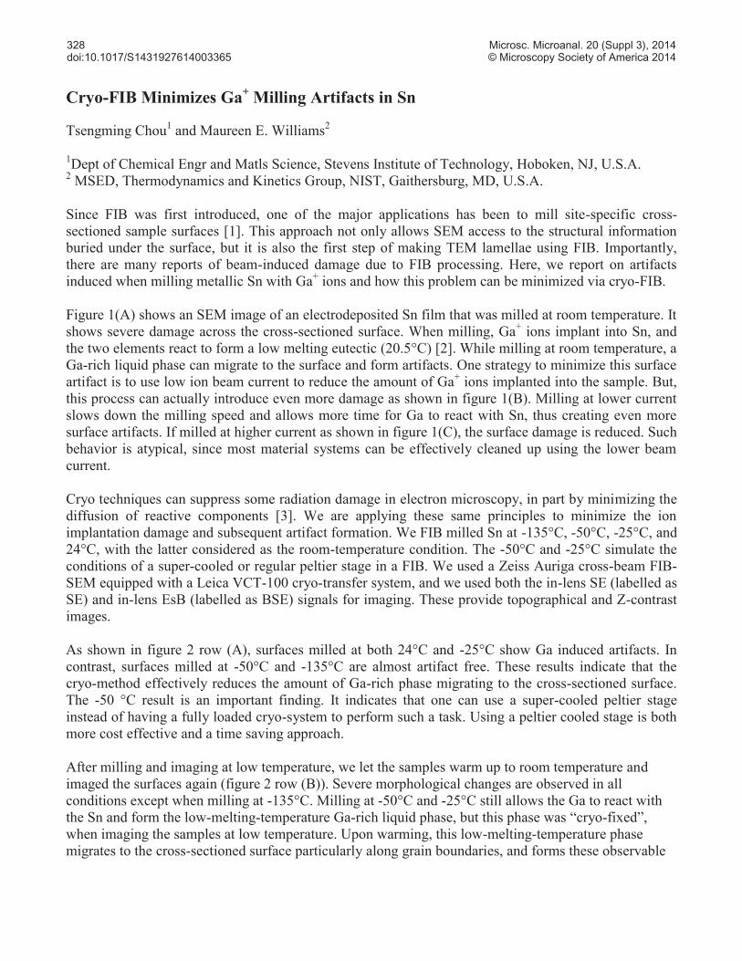
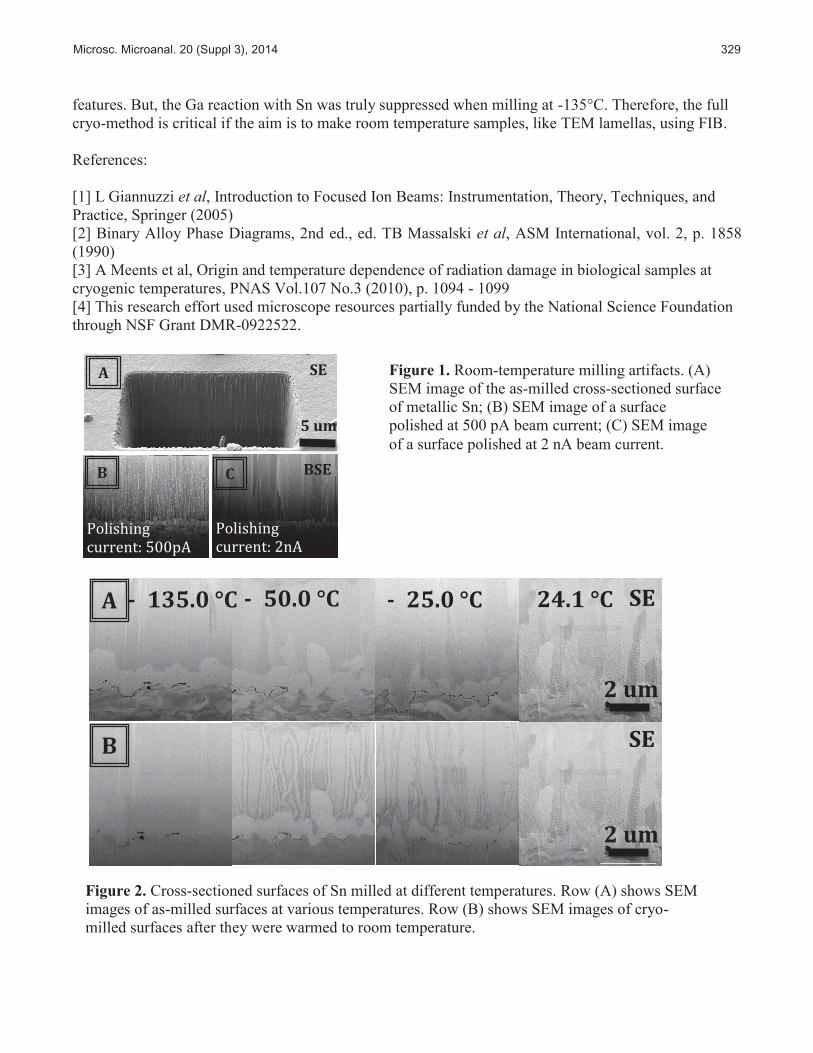
1Dept of Chemical Engr and Matls Science, Stevens Institute of Technology, Hoboken, NJ, U.S.A. 2 MSED, Thermodynamics and Kinetics Group, NIST, Gaithersburg, MD, U.S.A. Since FIB was first introduced, one of the major applications has been to mill site-specific cross-sectioned sample surfaces [1]. This approach not only allows SEM access to the structural information buried under the surface, but it is also the first step of making TEM lamellae using FIB. Importantly, there are many reports of beam-induced damage due to FIB processing. Here, we report on artifacts induced when milling metallic Sn with Ga+ ions and how this problem can be minimized via cryo-FIB. Figure 1(A) shows an SEM image of an electrodeposited Sn film that was milled at room temperature. It shows severe damage across the cross-sectioned surface. When milling, Ga+ ions implant into Sn, and the two elements react to form a low melting eutectic (20.5°C) [2]. While milling at room temperature, a Ga-rich liquid phase can migrate to the surface and form artifacts. One strategy to minimize this surface artifact is to use low ion beam current to reduce the amount of Ga+ ions implanted into the sample. But, this process can actually introduce even more damage as shown in figure 1(B). Milling at lower current slows down the milling speed and allows more time for Ga to react with Sn, thus creating even more surface artifacts. If milled at higher current as shown in figure 1(C), the surface damage is reduced. Such behavior is atypical, since most material systems can be effectively cleaned up using the lower beam current. Cryo techniques can suppress some radiation damage in electron microscopy, in part by minimizing the diffusion of reactive components [3]. We are applying these same principles to minimize the ion implantation damage and subsequent artifact formation. We FIB milled Sn at -135°C, -50°C, -25°C, and 24°C, with the latter considered as the room-temperature condition. The -50°C and -25°C simulate the conditions of a super-cooled or regular peltier stage in a FIB. We used a Zeiss Auriga cross-beam FIB-SEM equipped with a Leica VCT-100 cryo-transfer system, and we used both the in-lens SE (labelled as SE) and in-lens EsB (labelled as BSE) signals for imaging. These provide topographical and Z-contrast images. As shown in figure 2 row (A), surfaces milled at both 24°C and -25°C show Ga induced artifacts. In contrast, surfaces milled at -50°C and -135°C are almost artifact free. These results indicate that the cryo-method effectively reduces the amount of Ga-rich phase migrating to the cross-sectioned surface. The -50 °C result is an important finding. It indicates that one can use a super-cooled peltier stage instead of having a fully loaded cryo-system to perform such a task. Using a peltier cooled stage is both more cost effective and a time saving approach. After milling and imaging at low temperature, we let the samples warm up to room temperature and imaged the surfaces again (figure 2 row (B)). Severe morphological changes are observed in all conditions except when milling at -135°C. Milling at -50°C and -25°C still allows the Ga to react with the Sn and form the low-melting-temperature Ga-rich liquid phase, but this phase was cryo-fixed , when imaging the samples at low temperature. Upon warming, this low-melting-temperature phase migrates to the cross-sectioned surface particularly along grain boundaries, and forms these observable
328doi:10.1017/S1431927614003365
Microsc. Microanal. 20 (Suppl 3), 2014© Microscopy Society of America 2014
features. But, the Ga reaction with Sn was truly suppressed when milling at -135°C. Therefore, the full cryo-method is critical if the aim is to make room temperature samples, like TEM lamellas, using FIB. References: [1] L Giannuzzi et al, Introduction to Focused Ion Beams: Instrumentation, Theory, Techniques, and Practice, Springer (2005) [2] Binary Alloy Phase Diagrams, 2nd ed., ed. TB Massalski et al, ASM International, vol. 2, p. 1858 (1990) [3] A Meents et al, Origin and temperature dependence of radiation damage in biological samples at cryogenic temperatures, PNAS Vol.107 No.3 (2010), p. 1094 - 1099 [4] This research effort used microscope resources partially funded by the National Science Foundation through NSF Grant DMR-0922522.
Figure 1. Room-temperature milling artifacts. (A) SEM image of the as-milled cross-sectioned surface of metallic Sn; (B) SEM image of a surface polished at 500 pA beam current; (C) SEM image of a surface polished at 2 nA beam current.
Figure 2. Cross-sectioned surfaces of Sn milled at different temperatures. Row (A) shows SEM images of as-milled surfaces at various temperatures. Row (B) shows SEM images of cryo-milled surfaces after they were warmed to room temperature.
329Microsc. Microanal. 20 (Suppl 3), 2014