Embed Size (px)
Citation preview
CSCE 612: VLSI System Design
Instructor: Jason D. Bakos
VLSI System Design 2
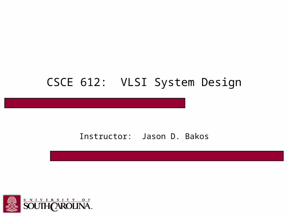
MOSFET Theory
p-type body: majority carriers
are holesaccumulation
mode
Vt depends on doping and tox
VLSI System Design 3
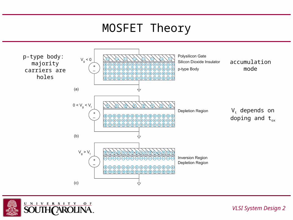
Regions of Operation
Gate to channel:
Vgs near source
Vgd near drain
Switching delay is determined by:
• time required to charge/discharge gate
• time for current to travel across channel
drain
VLSI System Design 4
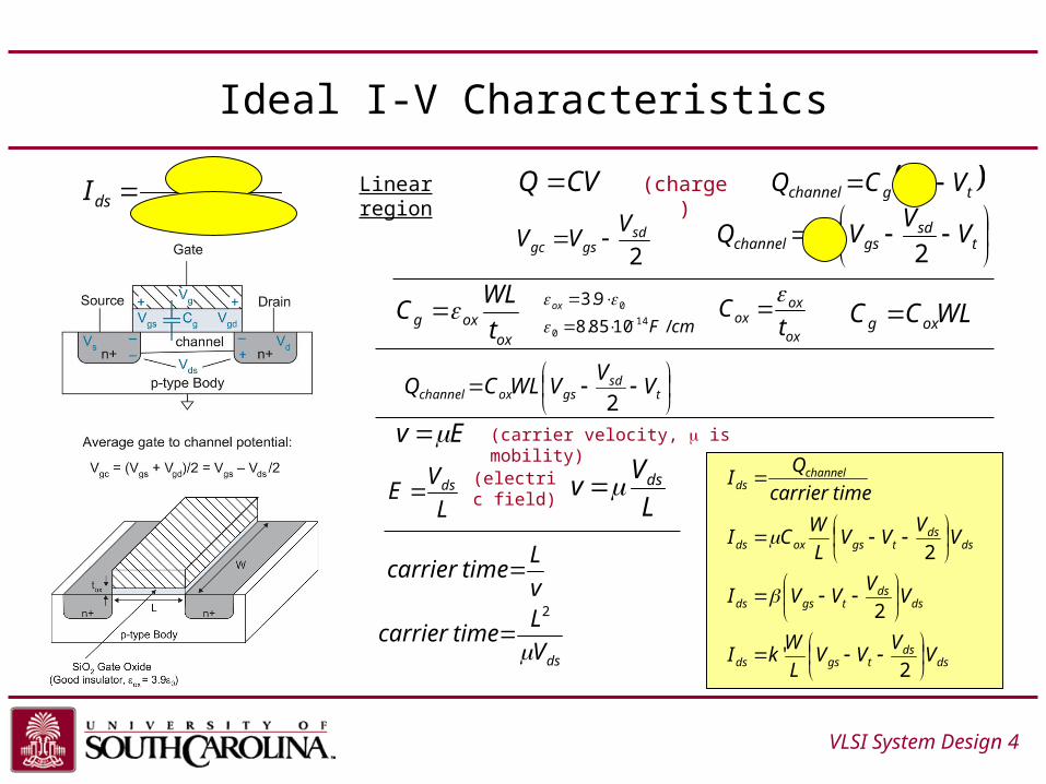
Ideal I-V Characteristics
CVQ tgcgchannel VVCQ
2sd
gsgc
VVV
Linear region
oxoxg t
WLC 09.3 ox
cmF /1085.8 140
Ev
L
VE ds
v
Ltimecarrier
dsds
tgsds
dsds
tgsds
dsds
tgsoxds
channelds
VV
VVL
WkI
VV
VVI
VV
VVL
WCI
timecarrier
QI
2'
2
2
(charge)
(carrier velocity, is mobility)
ox
oxox tC
t
sdgsgchannel VV
VCQ2
WLCC oxg
t
sdgsoxchannel VV
VWLCQ2
L
Vv ds(electric
field)
dsV
Ltimecarrier
2
timecarrier
QI channelds
VLSI System Design 5
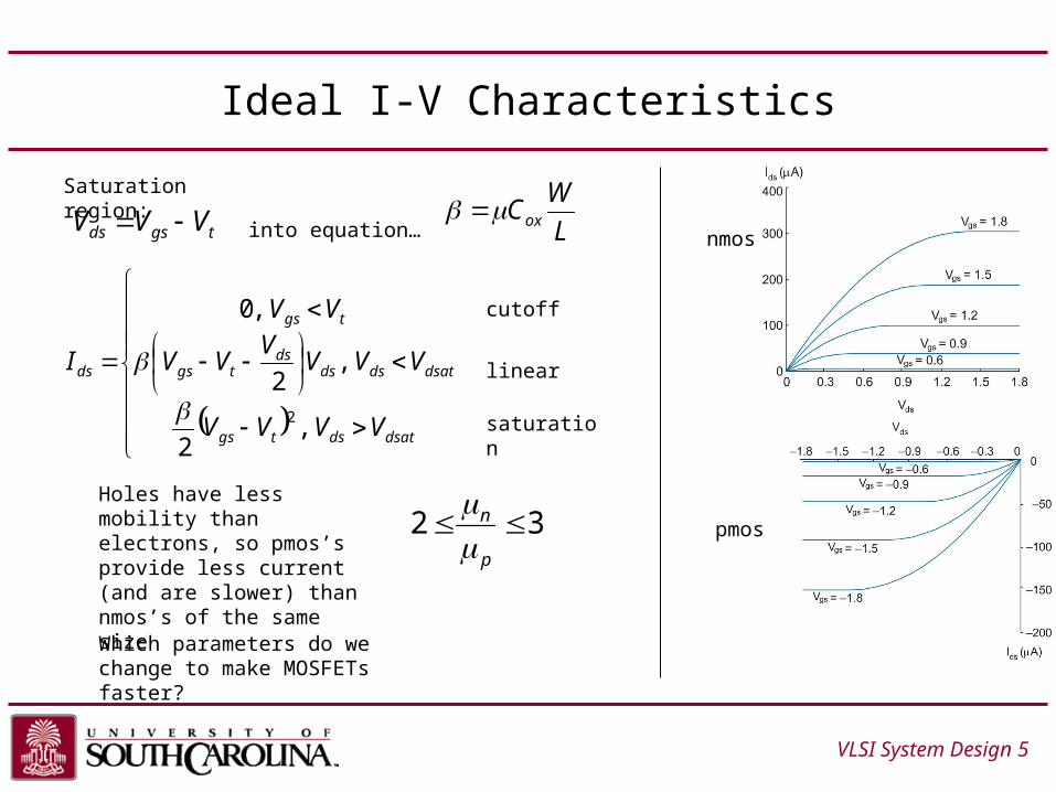
Ideal I-V Characteristics
tgsds VVV
dsatdstgs
dsatdsdsds
tgs
tgs
ds
VVVV
VVVV
VV
VV
I
,2
,2
,0
2
Saturation region:
into equation…
cutoff
linear
saturation
nmos
pmos32 p
n
Holes have less mobility
than electrons, so pmos’s provide less current (and are slower) than nmos’s of the same size
Which parameters do we change to make MOSFETs faster?
L
WCox
VLSI System Design 6
Nonideal I-V Effects
• Velocity saturation and mobility degradation– Lower Ids than expected
• At high lateral field strength (Vds/L), carrier velocity stops increasing linearly with field strength
• At high vertical field strength (Vgs / tox) the carriers scatter more often
• Channel length modulation– Saturation current increases with higher Vds
• Subthreshold conduction– Current drops exponentially when Vgs drops below Vt (not zero)
• Body effect– Vt affected by source voltage relative to body voltage
• Junction leakage– S/D leaks current into substrate/well
• Tunneling– Gate current due to thin gate oxides
• Temperature dependence– Mobility and threshold voltage decrease with rising temperature
VLSI System Design 7
C-V Characteristics
• Capacitors are bad– Slow down circuit (need to use more power), creates crosstalk
(noise)
• Gate is a good capacitor– Gate is one plate, channel is the other– Needed for operation: attracts charge to invert channel
• Source/drain are also capacitors to body (p-n junction)– Parasitic capacitance– “Diffusion capacitance”– Depends on diffusion area, perimeter, depth, doping levels,
and voltage• Make as small as possible (also reduces resistance)
VLSI System Design 8
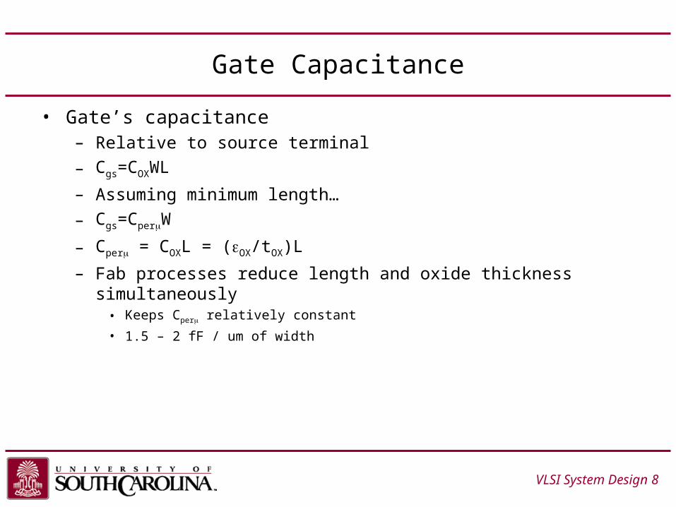
Gate Capacitance
• Gate’s capacitance– Relative to source terminal
– Cgs=COXWL
– Assuming minimum length…
– Cgs=CperW
– Cper = COXL = (OX/tOX)L
– Fab processes reduce length and oxide thickness simultaneously
• Keeps Cper relatively constant
• 1.5 – 2 fF / um of width
VLSI System Design 9
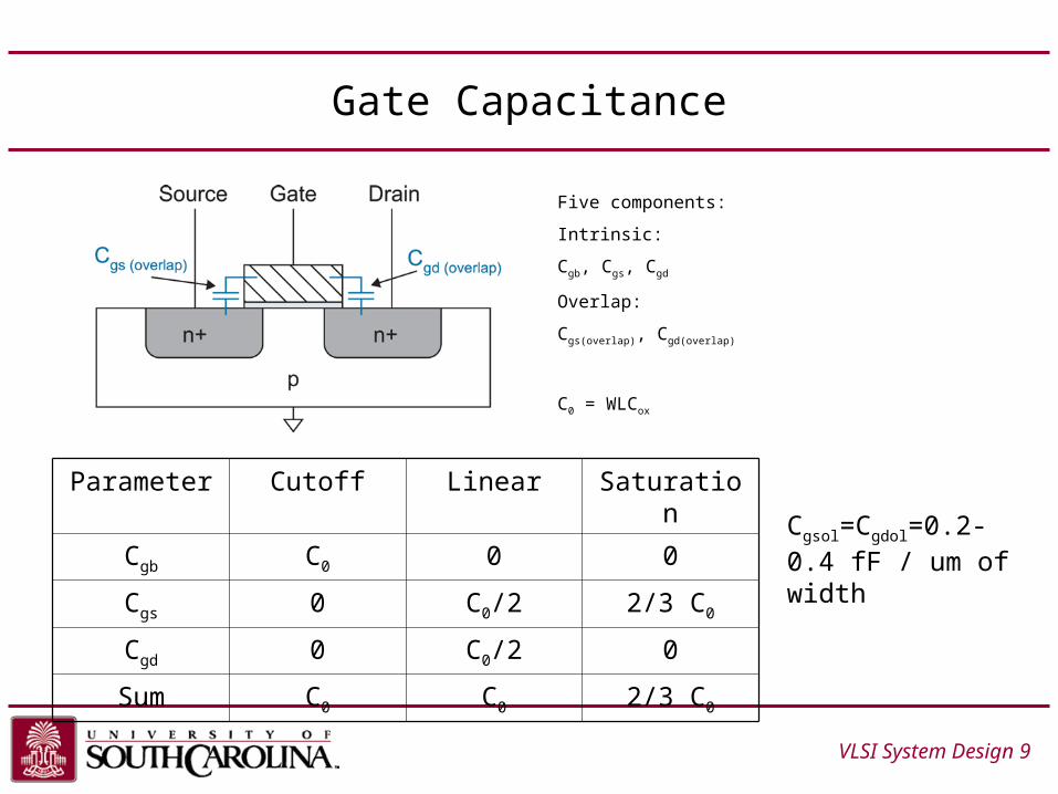
Gate Capacitance
Five components:
Intrinsic:
Cgb, Cgs, Cgd
Overlap:
Cgs(overlap), Cgd(overlap)
C0 = WLCox
Parameter Cutoff Linear Saturation
Cgb C0 0 0
Cgs 0 C0/2 2/3 C0
Cgd 0 C0/2 0
Sum C0 C0 2/3 C0
Cgsol=Cgdol=0.2-0.4 fF / um of width
VLSI System Design 10
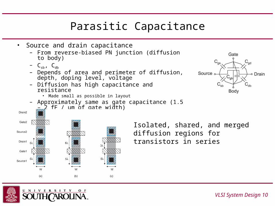
Parasitic Capacitance
• Source and drain capacitance– From reverse-biased PN junction (diffusion to
body)– Csb, Cdb
– Depends of area and perimeter of diffusion, depth, doping level, voltage
– Diffusion has high capacitance and resistance• Made small as possible in layout
– Approximately same as gate capacitance (1.5 – 2 fF / um of gate width)
Isolated, shared, and merged diffusion regions for transistors in series
VLSI System Design 11
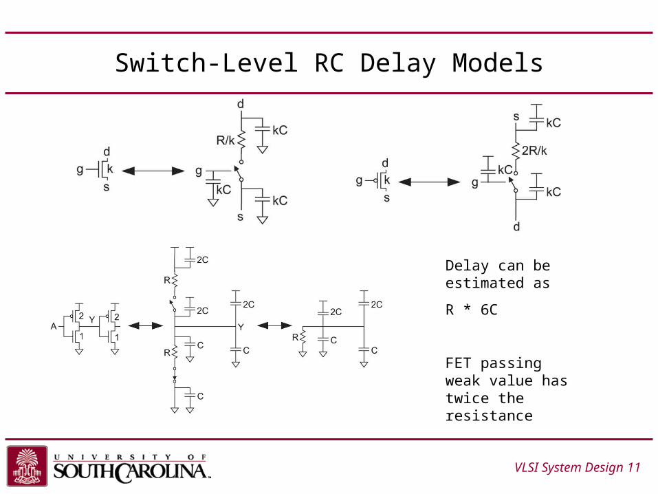
Switch-Level RC Delay Models
Delay can be estimated as
R * 6C
FET passing weak value has twice the resistance