Embed Size (px)
Citation preview
Cu–C60 interaction and nano-composite structures
J.G. Hou* , Xiang Li, Haiqian Wang, Bing Wang
Structure Research Laboratory, University of Science and Technology of China, Hefei 230026, Anhui, People’s Republic of China
Abstract
Experimental evidences for the formation of amorphous-like Cu–C60 interface compounds were reported. Cu–C60 nano-composite films were prepared by co-deposition method. The mechanism for the electrical transport in the compound is thehopping conduction and the magnitude of the conductivity increases, while the activation energy decreases with the increasingof Cu ratio. There is a transition at about 260 K in the curves of conductivity versus temperature, indicating that the transportmechanisms are related to the rotational order–disorder transition of C60 molecules.q 2000 Elsevier Science Ltd. All rightsreserved.
Keywords: A. Fullerene; A. Metals; A. Nanostructures; D. Electrical properties
1. Introduction
Since the discovery of a method for synthesis of C60 inmacroscopic quantities [1], C60–metal interaction has beenone of the main subjects in fullerene research. The interac-tions of fullerene with metals can be classified according toas to whether they form compounds or form phase-separatedsolids [2]. In the alkali- or alkali-earth metal fullerides,metal atoms are intercalated into the host C60 lattice andact as the electron donors, superconductivity was discoveredin the intercalated compounds where three electrons aretransferred from the metals to each C60 molecule [3].While, for the phase-separated solids, no solid solution isformed due to the high cohesive energy of the metals otherthan alkali or alkali-earth metals. However, limited inter-mixing and charge transfer between most of the metals andC60 is still possible, since the work functions for most of themetals have a low value [4–8]. The charge transfer acrossthe metal–C60 interface may provide an opportunity to formnovel fullerene interface compounds in some kind of low-dimensional structures. Motivated by interest in metal–C60
compounds, we explored the possibility for making Cu–C60
composites via thin film route and studied the structural andphysical properties with different techniques.
2. Experimental
Cu–C60 nano-structure films were prepared by co-depo-sition method in vacuum at a base pressure of about 4×1024 Pa: High purity Cu (.99.99%) and C60 (.99.9%)powder were used. Before deposition, C60 was degassed inhigh vacuum at 2008C for about 2 h. The substrates werefreshly cut (001) NaCl single crystals. For conductivitystudies, gold electrodes, 50 nm thick, were pre-depositedon the substrate surface. A quartz thickness monitormeasured the deposition rates of the metal and C60. Byadjusting the source temperatures of metal and fullerene,and thus the deposition rate, C60/Cu composite films withdifferent ratio of metal to C60 were obtained. The tempera-ture of the substrates was kept at room temperature duringthe film growth. After deposition the films were annealed at1608C in the same vacuum for about 5 h, and the electricalconductivity of the film was monitored during the annealing.At the early stage of annealing, the conductivity of the filmincreases quickly and then reaches to a stable value. Thenthe temperature was cooling down slowly and electricalconductivity measurements were carried out by the standardfour-probe in line method. The temperature of the sampleholder was controlled, by adjusting the power of a smallheater and the flow rate of liquid nitrogen. The typical cool-ing rate during the measurements was about 1 K/min. Afterthe in-situ conductivity measurements, samples were trans-ferred quickly from the vacuum to a Raman apparatus formeasurement. The nominal thickness of the films for
Journal of Physics and Chemistry of Solids 61 (2000) 995–998
0022-3697/00/$ - see front matterq 2000 Elsevier Science Ltd. All rights reserved.PII: S0022-3697(99)00349-2
www.elsevier.nl/locate/jpcs
* Corresponding author. Tel.:186-551-360-2809; fax:186-551-360-2803.
E-mail address:[email protected] (J.G. Hou).
electrical measurement is about 100 nm. In order to evaluatethe microstructure of Cu–C60 composite film, thinner filmsof about 30 nm were prepared with the same depositionconditions. After deposition the NaCl substrate wasdissolved in distilled water and the films were put on coppergrids for transmission electron microscope (TEM) examina-tion.
3. Results and discussions
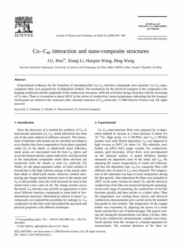
Fig. 1a shows the typical ln�s=sRT� / �1=T� curves ofCu–C60 films with different Cu/C60 ratio. A semiconductorbehavior of the conductivity versus temperature plots weretypically observed for most of the films in which the metalvolume fraction is under the percolation threshold, exceptthe film with high Cu/C60 ratio �NCu=NC60
� 80�: There is a
transition at about 260 K for all the semiconductor films. Itis noted that the linear relationship ln�s=sRT� / �1=T� wasobserved when the temperatures was lower than 250 K, andthe relation ln�s=sRT� / �1=T1=4� was observed for tempera-tures higher than 260 K (Fig. 1b). It is known that solid C60
undergoes a first-order phase transition, at about 260 K,from face-center-cubic structure (fcc) to simple cubic struc-ture (sc) [9]. The result indicated that the conductionmechanism depend on the C60 structure. From Fig. 1 wecan also find that the magnitude of the conductivityincreases, while the activation energy decreases with theincreasing of Cu ratio. The values of conductivity of thesefilms (typically in the range of 1022–102 S cm21) aremuch higher than that of the pristine C60 solid(,1027 S cm21).
In order to understand the conduction mechanism of thecomposite films, it is necessary to study the microstructure
J.G. Hou et al. / Journal of Physics and Chemistry of Solids 61 (2000) 995–998996
Fig. 1. Temperature dependent normalized conductivities of the films with different Cu/C60 ratio, the relations of ln�s� / �1=T� (a) and ln�s� /�1=T1=4� (b) were observed forT , 250 K andT . 260 K; respectively.
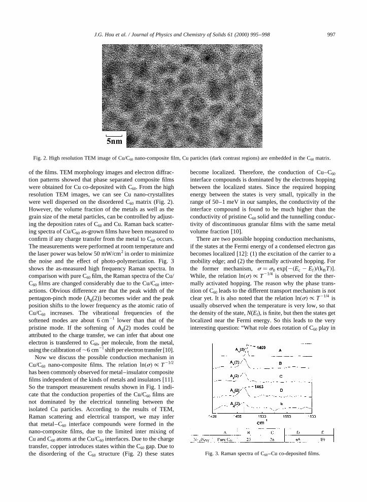
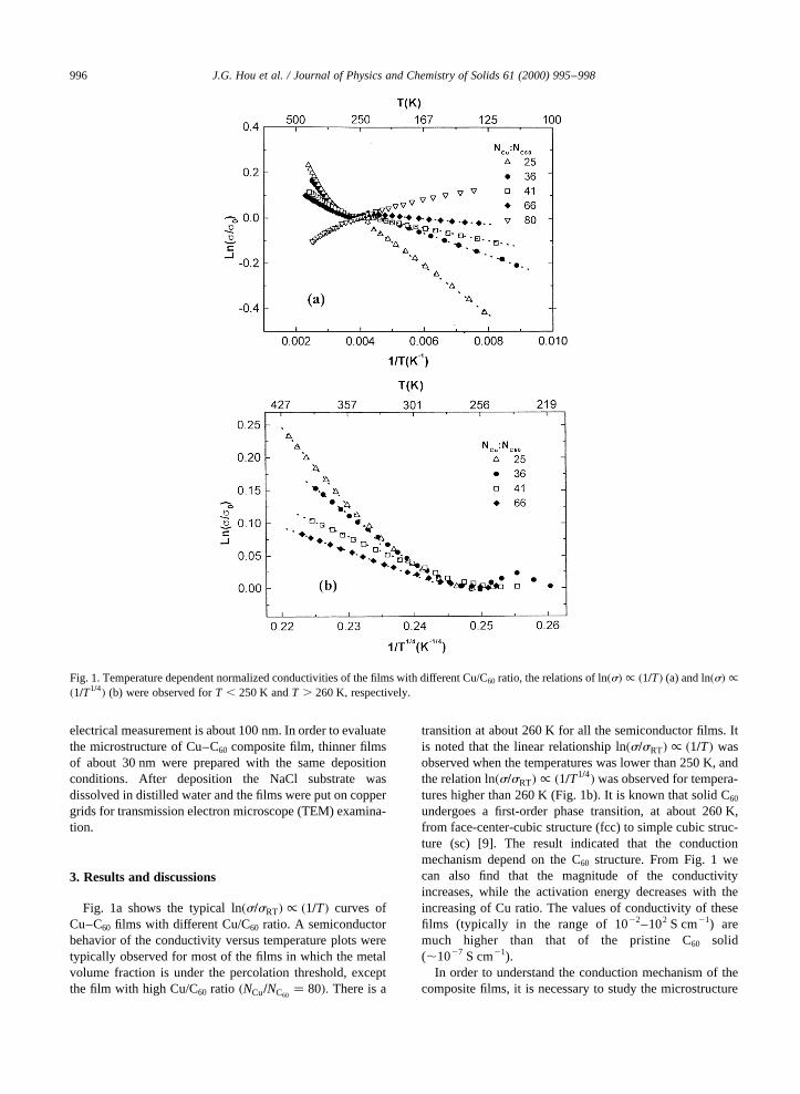
of the films. TEM morphology images and electron diffrac-tion patterns showed that phase separated composite filmswere obtained for Cu co-deposited with C60. From the highresolution TEM images, we can see Cu nano-crystalliteswere well dispersed on the disordered C60 matrix (Fig. 2).However, the volume fraction of the metals as well as thegrain size of the metal particles, can be controlled by adjust-ing the deposition rates of C60 and Cu. Raman back scatter-ing spectra of Cu/C60 as-grown films have been measured toconfirm if any charge transfer from the metal to C60 occurs.The measurements were performed at room temperature andthe laser power was below 50 mW/cm2 in order to minimizethe noise and the effect of photo-polymerization. Fig. 3shows the as-measured high frequency Raman spectra. Incomparison with pure C60 film, the Raman spectra of the Cu/C60 films are changed considerably due to the Cu/C60 inter-actions. Obvious difference are that the peak width of thepentagon-pinch mode (Ag(2)) becomes wider and the peakposition shifts to the lower frequency as the atomic ratio ofCu/C60 increases. The vibrational frequencies of thesoftened modes are about 6 cm21 lower than that of thepristine mode. If the softening of Ag(2) modes could beattributed to the charge transfer, we can infer that about oneelectron is transferred to C60, per molecule, from the metal,using the calibration of,6 cm21 shift per electron transfer [10].
Now we discuss the possible conduction mechanism inCu/C60 nano-composite films. The relation ln�s� / T21=2
has been commonly observed for metal–insulator compositefilms independent of the kinds of metals and insulators [11].So the transport measurement results shown in Fig. 1 indi-cate that the conduction properties of the Cu/C60 films arenot dominated by the electrical tunneling between theisolated Cu particles. According to the results of TEM,Raman scattering and electrical transport, we may inferthat metal–C60 interface compounds were formed in thenano-composite films, due to the limited inter mixing ofCu and C60 atoms at the Cu/C60 interfaces. Due to the chargetransfer, copper introduces states within the C60 gap. Due tothe disordering of the C60 structure (Fig. 2) these states
become localized. Therefore, the conduction of Cu–C60
interface compounds is dominated by the electrons hoppingbetween the localized states. Since the required hoppingenergy between the states is very small, typically in therange of 50–1 meV in our samples, the conductivity of theinterface compound is found to be much higher than theconductivity of pristine C60 solid and the tunnelling conduc-tivity of discontinuous granular films with the same metalvolume fraction [10].
There are two possible hopping conduction mechanisms,if the states at the Fermi energy of a condensed electron gasbecomes localized [12]: (1) the excitation of the carrier to amobility edge; and (2) the thermally activated hopping. Forthe former mechanism,s � s0 exp�2�Ec 2 Ef �=�kBT��:While, the relation ln�s� / T21=4 is observed for the ther-mally activated hopping. The reason why the phase trans-ition of C60 leads to the different transport mechanism is notclear yet. It is also noted that the relation ln�s� / T21=4 isusually observed when the temperature is very low, so thatthe density of the state,N(Ef), is finite, but then the states getlocalized near the Fermi energy. So this leads to the veryinteresting question: “What role does rotation of C60 play in
J.G. Hou et al. / Journal of Physics and Chemistry of Solids 61 (2000) 995–998 997
Fig. 3. Raman spectra of C60–Cu co-deposited films.
Fig. 2. High resolution TEM image of Cu/C60 nano-composite film, Cu particles (dark contrast regions) are embedded in the C60 matrix.
the localization of states in the Cu/C60 films?” Furtherstudies are underway in answering this.
4. Conclusions
Interesting structural and physical properties wereobserved in Cu/C60 nano-structures. The strong interactionbetween Cu and C60 not only leads to the charge transferfrom metal to C60 at the interface, but also form the Cu/C60
interface compound, which exhibits hopping conductivity.
Acknowledgements
The work is supported by the NSF of China.
References
[1] Kratschmer, et al., Nature 347 (1990) 354.[2] J.H. Weaver, D.M. Poirier, Fullerene fundamentals, in: H.
Ehreneich, F. Spaepen (Eds.), Solid State Physics, 48,Academic Press, Cambridge, 1994 chap. 1.
[3] Hebard, et al., Nature 350 (1991) 600.[4] M.R.C. Hunt, S. Modesti, P. Rudoli, R.E. Palmer, Phys. Rev.
B 51 (1995) 10 039.[5] Y. Maruyama, K. Ohno, Y. Kawazoe, Phys. Rev. B 52 (1994)
2070.[6] D. Owens, et al., Phys. Rev. B 51 (1994) 17 740.[7] Maxwell, et al., Phy. Rev. B 52 (1995) R5546.[8] Hebard, et al., Phys. Rev. B 50 (1994) 17 740.[9] T. David, et al., Phys. Rev. B 50 (1994) 5810.
[10] F. Gugenberger, et al., Phys. Rev. Lett. 69 (1992) 3774.[11] B. Abeles, et al., Adv. Phys. 24 (1975) 497.[12] N.F. Mott, Metal–Insulator Transitions, Taylor & Francis,
London, 1990.
J.G. Hou et al. / Journal of Physics and Chemistry of Solids 61 (2000) 995–998998


![Biomimetic Nano-Composite Actuator Based on Fullerene ... · Biomimetic Nano-Composite Actuator Based on Fullerene-Reinforced Nafion Ionic Polymer ... polymers[3], carbon nanotubes[4](https://img.pdfslide.net/doc/110x75/5afe37407f8b9a944d8e86d6/biomimetic-nano-composite-actuator-based-on-fullerene-nano-composite-actuator.jpg)