Embed Size (px)
Citation preview
CYPRESS PRODUCT SELECTOR GUIDE FLASH MEMORYFebruary 2016
PARALLEL NOR FLASH • SERIAL NOR FLASH • SLC NAND FLASH • e.MMC NAND FLASH • HYPERFLASH™

CYPRESS PRODUCT SELECTOR GUIDE
PSoC, CapSense, TrueTouch, SLIM, West Bridge, EZ-USB, HOTLink, MoBL, and RoboClock are registered trademarks and Antioch, Autobrite, AutoMoBL, AutoRate Receiver, CapSense Express, COMLINK, ConsuMoBL, enCoRe, EZ-Host, EZ-OTG, EZ-USB AT2LP, EZ-USB FX2LP, EZ-USB NX2LP, EZ-USB NX2LP-Flex, EZ-USB SX2, EZ-USB TX2, FailSafe, FullFlex, HOTLinkDX, HOTLink II, M8, MediaClock, MoBL-USB, No Bus Latency, NoBL, PacketClock, PREMIS, PRoC, PSoC Designer, PSoC Express, RAM9, SLIM, SpreadAware, Charger Armor, Tx Boost, WirelessUSB, WirelessUSB LP, WirelessUSB LR, WirelessUSB LS, HyperFlash, HyperBus, MirrorBit and Eclipse are trademarks of Cypress Semiconductor Corporation.
QDR RAMs and Quad Data Rate RAMs comprise a new family of products developed by Cypress, IDT, NEC, Renesas and Samsung. XScale is a registered trademark of Marvell, Inc. Rambus and Direct Rambus are registered trademarks of Rambus, Inc. All other product and company names mentioned in this document are the trademarks of their respective holders and may be registered in some jurisdictions.
© Copyright 2016 Cypress Semiconductor Corporation. All rights reserved.
The information contained herein is subject to change without notice. Cypress Semiconductor Corporation assumes no responsibility for the use of any circuitry other than circuitry embodied in a Cypress product. Nor does it convey or imply any license under patent or other rights. Cypress products are not warranted nor intended to be used for medical, life support, life saving, critical control or safety applications, unless pursuant to an express written agreement with Cypress. Furthermore, Cypress does not authorize its products for use as critical components in life-support systems where a malfunction or failure may reasonably be expected to result in significant injury to the user. The inclusion of Cypress products in life-support systems application implies that the manufacturer assumes all risk of such use and in doing so indemnifies Cypress against all charges.
Products, specifications and availability are subject to change. Please contact your local sales representative or visit the Cypress website at www.cypress.com for the most current information.
CYPRESS PRODUCT SELECTOR GUIDE
FLASH MEMORY . . . . . . . . . . . . . . . . . . . . . . . . . . . . . . . . . . . . . . . . . . . . . . . . . . . . . . . . . . . . . . . . . . . . . . . . . . . . . . . . . . 2Flash Product Portfolio . . . . . . . . . . . . . . . . . . . . . . . . . . . . . . . . . . . . . . . . . . . . . . . . . . . . . . . . . . . . . . . . . . . . . . . . . . 3Flash Memory Guide. . . . . . . . . . . . . . . . . . . . . . . . . . . . . . . . . . . . . . . . . . . . . . . . . . . . . . . . . . . . . . . . . . . . . . . . . . . 4KL/KS Families . . . . . . . . . . . . . . . . . . . . . . . . . . . . . . . . . . . . . . . . . . . . . . . . . . . . . . . . . . . . . . . . . . . . . . . . . . . . . . . 5GL Family . . . . . . . . . . . . . . . . . . . . . . . . . . . . . . . . . . . . . . . . . . . . . . . . . . . . . . . . . . . . . . . . . . . . . . . . . . . . . . . . . . 5AL/JL/PL Families . . . . . . . . . . . . . . . . . . . . . . . . . . . . . . . . . . . . . . . . . . . . . . . . . . . . . . . . . . . . . . . . . . . . . . . . . . . . . 6CD/CL Family. . . . . . . . . . . . . . . . . . . . . . . . . . . . . . . . . . . . . . . . . . . . . . . . . . . . . . . . . . . . . . . . . . . . . . . . . . . . . . . . 6AS Family . . . . . . . . . . . . . . . . . . . . . . . . . . . . . . . . . . . . . . . . . . . . . . . . . . . . . . . . . . . . . . . . . . . . . . . . . . . . . . . . . . 7WS/NS/VS/XS Families . . . . . . . . . . . . . . . . . . . . . . . . . . . . . . . . . . . . . . . . . . . . . . . . . . . . . . . . . . . . . . . . . . . . . . . . 7FL Family . . . . . . . . . . . . . . . . . . . . . . . . . . . . . . . . . . . . . . . . . . . . . . . . . . . . . . . . . . . . . . . . . . . . . . . . . . . . . . . . . . . 8FS Family . . . . . . . . . . . . . . . . . . . . . . . . . . . . . . . . . . . . . . . . . . . . . . . . . . . . . . . . . . . . . . . . . . . . . . . . . . . . . . . . . . . 8ML/MS Families . . . . . . . . . . . . . . . . . . . . . . . . . . . . . . . . . . . . . . . . . . . . . . . . . . . . . . . . . . . . . . . . . . . . . . . . . . . . . . 941-IBI Family . . . . . . . . . . . . . . . . . . . . . . . . . . . . . . . . . . . . . . . . . . . . . . . . . . . . . . . . . . . . . . . . . . . . . . . . . . . . . . . 10Ordering Part Number Construction . . . . . . . . . . . . . . . . . . . . . . . . . . . . . . . . . . . . . . . . . . . . . . . . . . . . . . . . . . . . . . . 11Universal Footprint . . . . . . . . . . . . . . . . . . . . . . . . . . . . . . . . . . . . . . . . . . . . . . . . . . . . . . . . . . . . . . . . . . . . . . . . . . . 123.0V HyperFlash Memory . . . . . . . . . . . . . . . . . . . . . . . . . . . . . . . . . . . . . . . . . . . . . . . . . . . . . . . . . . . . . . . . . . . . . . 131.8V HyperFlash Memory . . . . . . . . . . . . . . . . . . . . . . . . . . . . . . . . . . . . . . . . . . . . . . . . . . . . . . . . . . . . . . . . . . . . . . 133.0V Parallel Flash Memory . . . . . . . . . . . . . . . . . . . . . . . . . . . . . . . . . . . . . . . . . . . . . . . . . . . . . . . . . . . . . . . . . . . . . 142.5V Parallel Flash Memory . . . . . . . . . . . . . . . . . . . . . . . . . . . . . . . . . . . . . . . . . . . . . . . . . . . . . . . . . . . . . . . . . . . . 151.8V Parallel ADP Flash Memory . . . . . . . . . . . . . . . . . . . . . . . . . . . . . . . . . . . . . . . . . . . . . . . . . . . . . . . . . . . . . . . . . 151.8V Muxed ADM Flash Memory . . . . . . . . . . . . . . . . . . . . . . . . . . . . . . . . . . . . . . . . . . . . . . . . . . . . . . . . . . . . . . . . . 151.8 Muxed AADM Flash Memory . . . . . . . . . . . . . . . . . . . . . . . . . . . . . . . . . . . . . . . . . . . . . . . . . . . . . . . . . . . . . . . . 153.0V & 1.8V SPI Flash Memory. . . . . . . . . . . . . . . . . . . . . . . . . . . . . . . . . . . . . . . . . . . . . . . . . . . . . . . . . . . . . . . . . . . 163.0V NAND Memory . . . . . . . . . . . . . . . . . . . . . . . . . . . . . . . . . . . . . . . . . . . . . . . . . . . . . . . . . . . . . . . . . . . . . . . . . 171.8V NAND Memory . . . . . . . . . . . . . . . . . . . . . . . . . . . . . . . . . . . . . . . . . . . . . . . . . . . . . . . . . . . . . . . . . . . . . . . . . 181.8V NAND MCP Solutions . . . . . . . . . . . . . . . . . . . . . . . . . . . . . . . . . . . . . . . . . . . . . . . . . . . . . . . . . . . . . . . . . . . . . 193.0V e.MMC NAND Flash . . . . . . . . . . . . . . . . . . . . . . . . . . . . . . . . . . . . . . . . . . . . . . . . . . . . . . . . . . . . . . . . . . . . . 193.0V Parallel ADP MCP Solutions . . . . . . . . . . . . . . . . . . . . . . . . . . . . . . . . . . . . . . . . . . . . . . . . . . . . . . . . . . . . . . . . . 191.8V Parallel ADP MCP Solutions . . . . . . . . . . . . . . . . . . . . . . . . . . . . . . . . . . . . . . . . . . . . . . . . . . . . . . . . . . . . . . . . . 191.8V Muxed ADM MCP Solutions . . . . . . . . . . . . . . . . . . . . . . . . . . . . . . . . . . . . . . . . . . . . . . . . . . . . . . . . . . . . . . . . . 191.8 Muxed AADM MCP Solutions . . . . . . . . . . . . . . . . . . . . . . . . . . . . . . . . . . . . . . . . . . . . . . . . . . . . . . . . . . . . . . . . 19Long-Term Memory Portfolio . . . . . . . . . . . . . . . . . . . . . . . . . . . . . . . . . . . . . . . . . . . . . . . . . . . . . . . . . . . . . . . . . . . . 20
TABLE OF CONTENTS
www.cypress.com 2 www.cypress.com 3
CYPRESS PRODUCT SELECTOR GUIDE
CYPRESS FLASH MEMORY
Cypress offers a broad portfolio of reliable high-performance Flash Memories for program-code and data storage. Cypress is No. 1 in NOR Flash Memory and has more than 20 years of experience. We are committed to providing highly-reliable, AEC-Q100 qualified products that meet the most rigorous automotive standards. We continue to invest heavily to bring new, innovative Flash Memory products to market, and assure long-term supply for our portfolio. Cypress complements all its products with world-class customer support.
CYPRESS NOR FLASH MEMORY
Cypress NOR Flash provides the fast, low-latency random access and high read bandwidth required by high-performance systems to access program memory and data as fast as possible. Cypress offers a full portfolio of NOR Flash including parallel interface and low-pin-count serial interface products. Cypress NOR Flash Memories offer the industry’s fastest program and sector erase times.
NOR FLASH PORTFOLIO SUMMARY
Interface Parallel Quad SPI Dual-Quad SPI HyperBus™
Density 8Mb - 2Gb 16Mb - 1Gb 256Mb - 1Gb 128Mb - 512Mb
Read Bandwidth (max) 102 MBps 80 MBps 160 MBps 333 MBps
Voltage 3.0V, 2.5V, 1.8V 3.0V, 1.8V 3.0V 3.0V, 1.8V
Temperature Ranges
Industrial: -40°C to +85°CIndustrial-plus: -40°C to +105°C
Extended: -40°C to +125°CHot: -40°C to +145°C
Industrial: -40°C to +85°CIndustrial-plus: -40°C to +105°C
Extended: -40°C to +125°C
Automotive Support AEC-Q100, PPAP
CYPRESS NAND FLASH MEMORY
Cypress’s portfolio of NAND Flash products complements its NOR Flash portfolio for embedded applications. Cypress applies stringent processes for qualification and testing across an extended operating temperature range for its NAND products. All of Cypress’s NAND products are backed by Cypress’s world-class customer support and commitment for longevity of supply. Cypress’s NAND products include SLC NAND and e.MMC NAND Flash Memories.
SLC NAND FLASH PORTFOLIO SUMMARY
Density 1Gb - 16Gb
Interface ONFI 1.0
Bandwidth 40 MBps
Endurance 100,000 P/E cycles (typical)
Voltage 3.0V, 1.8V
Temperature RangesIndustrial: -40°C to +85°CIndustrial Plus: -40°C to +105°C
Automotive Support AEC-Q100, PPAP
ECC Requirement 1-bit, 4-bit
e.MMC NAND FLASH PORTFOLIO SUMMARY
Density 8GB - 16GB
Interface e.MMC 4.51
Bandwidth 200 MBps
Voltage 3.0V
Temperature RangesEmbedded: -25°C to +85°CIndustrial: -40°C to +85°C
Features Health Monitoring
www.cypress.com 2 www.cypress.com 3
CYPRESS PRODUCT SELECTOR GUIDE
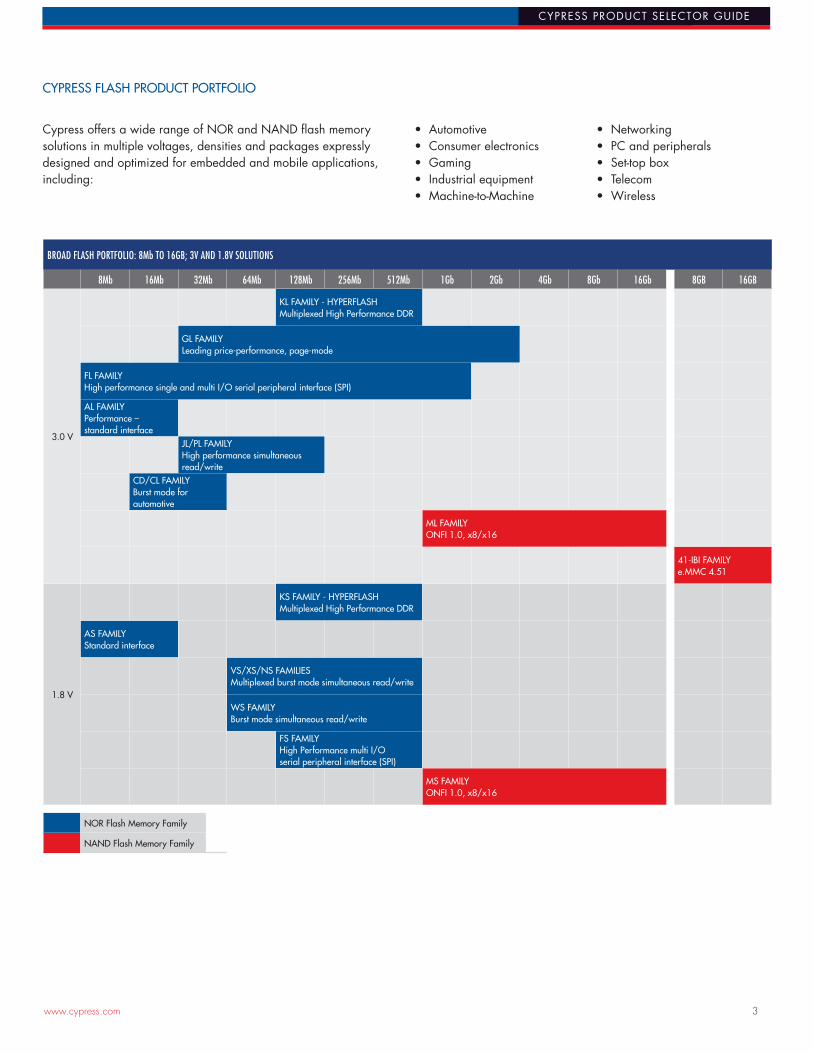
CYPRESS FLASH PRODUCT PORTFOLIO
Cypress offers a wide range of NOR and NAND flash memory solutions in multiple voltages, densities and packages expressly designed and optimized for embedded and mobile applications, including:
• Automotive• Consumer electronics• Gaming• Industrial equipment• Machine-to-Machine
• Networking• PC and peripherals• Set-top box• Telecom• Wireless
BROAD FLASH PORTFOLIO: 8Mb TO 16GB; 3V AND 1.8V SOLUTIONS
8Mb 16Mb 32Mb 64Mb 128Mb 256Mb 512Mb 1Gb 2Gb 4Gb 8Gb 16Gb 8GB 16GB
3.0 V
KL FAMILY - HYPERFLASHMultiplexed High Performance DDR
GL FAMILYLeading price-performance, page-mode
FL FAMILYHigh performance single and multi I/O serial peripheral interface (SPI)
AL FAMILYPerformance – standard interface
JL/PL FAMILYHigh performance simultaneous read/write
CD/CL FAMILYBurst mode for automotive
ML FAMILYONFI 1.0, x8/x16
41-IBI FAMILYe.MMC 4.51
1.8 V
KS FAMILY - HYPERFLASHMultiplexed High Performance DDR
AS FAMILYStandard interface
VS/XS/NS FAMILIESMultiplexed burst mode simultaneous read/write
WS FAMILYBurst mode simultaneous read/write
FS FAMILYHigh Performance multi I/Oserial peripheral interface (SPI)
MS FAMILYONFI 1.0, x8/x16
NOR Flash Memory Family
NAND Flash Memory Family
www.cypress.com 4 www.cypress.com 5
CYPRESS PRODUCT SELECTOR GUIDE
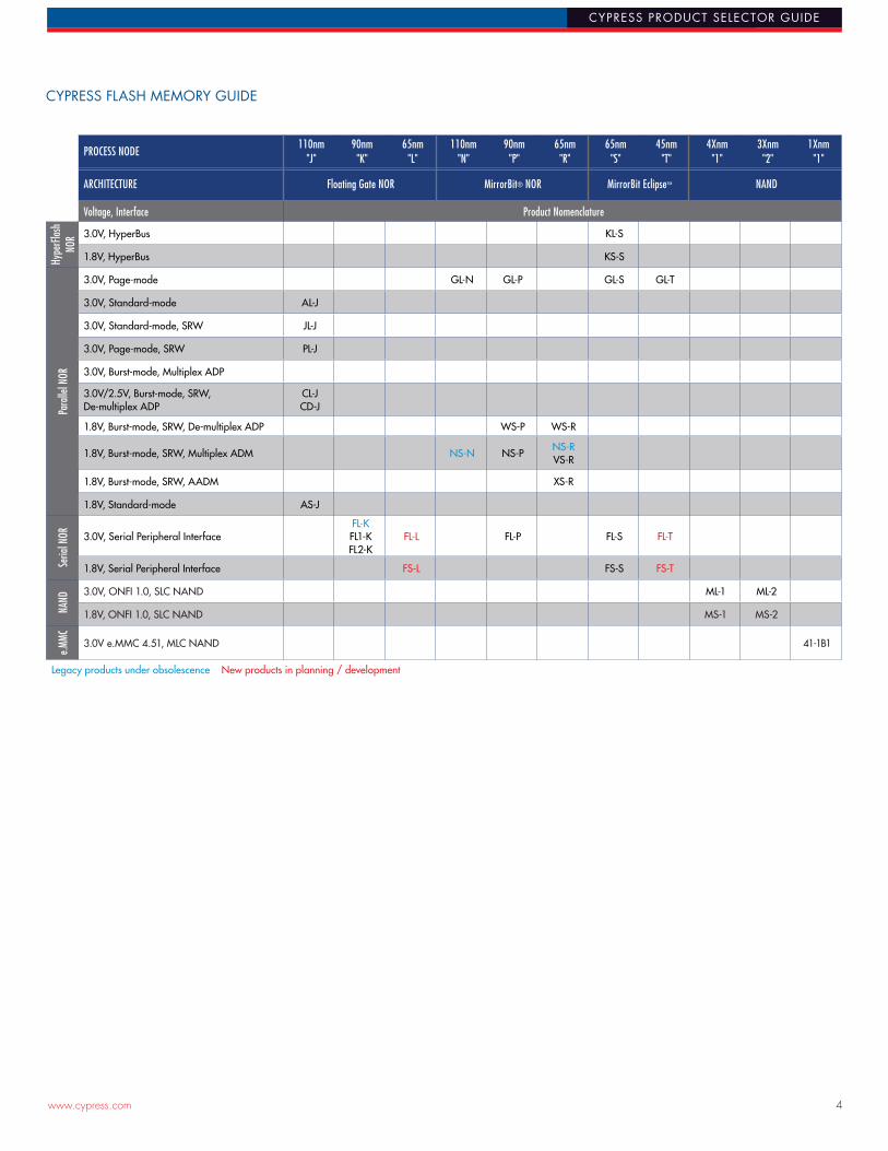
CYPRESS FLASH MEMORY GUIDE
PROCESS NODE110nm
"J"90nm
"K"65nm
"L"110nm
"N"90nm
"P"65nm
"R"65nm
"S"45nm
"T"4Xnm
"1"3Xnm
"2"1Xnm
"1"
ARCHITECTURE Floating Gate NOR MirrorBit® NOR MirrorBit Eclipse™ NAND
Voltage, Interface Product Nomenclature
Hype
rFlas
h NO
R 3.0V, HyperBus KL-S
1.8V, HyperBus KS-S
Para
llel N
OR
3.0V, Page-mode GL-N GL-P GL-S GL-T
3.0V, Standard-mode AL-J
3.0V, Standard-mode, SRW JL-J
3.0V, Page-mode, SRW PL-J
3.0V, Burst-mode, Multiplex ADP
3.0V/2.5V, Burst-mode, SRW, De-multiplex ADP
CL-JCD-J
1.8V, Burst-mode, SRW, De-multiplex ADP WS-P WS-R
1.8V, Burst-mode, SRW, Multiplex ADM NS-N NS-PNS-RVS-R
1.8V, Burst-mode, SRW, AADM XS-R
1.8V, Standard-mode AS-J
Seria
l NOR 3.0V, Serial Peripheral Interface
FL-KFL1-KFL2-K
FL-L FL-P FL-S FL-T
1.8V, Serial Peripheral Interface FS-L FS-S FS-T
NAND
3.0V, ONFI 1.0, SLC NAND ML-1 ML-2
1.8V, ONFI 1.0, SLC NAND MS-1 MS-2
e.MMC 3.0V e.MMC 4.51, MLC NAND 41-1B1
Legacy products under obsolescence New products in planning / development
www.cypress.com 4 www.cypress.com 5
CYPRESS PRODUCT SELECTOR GUIDE
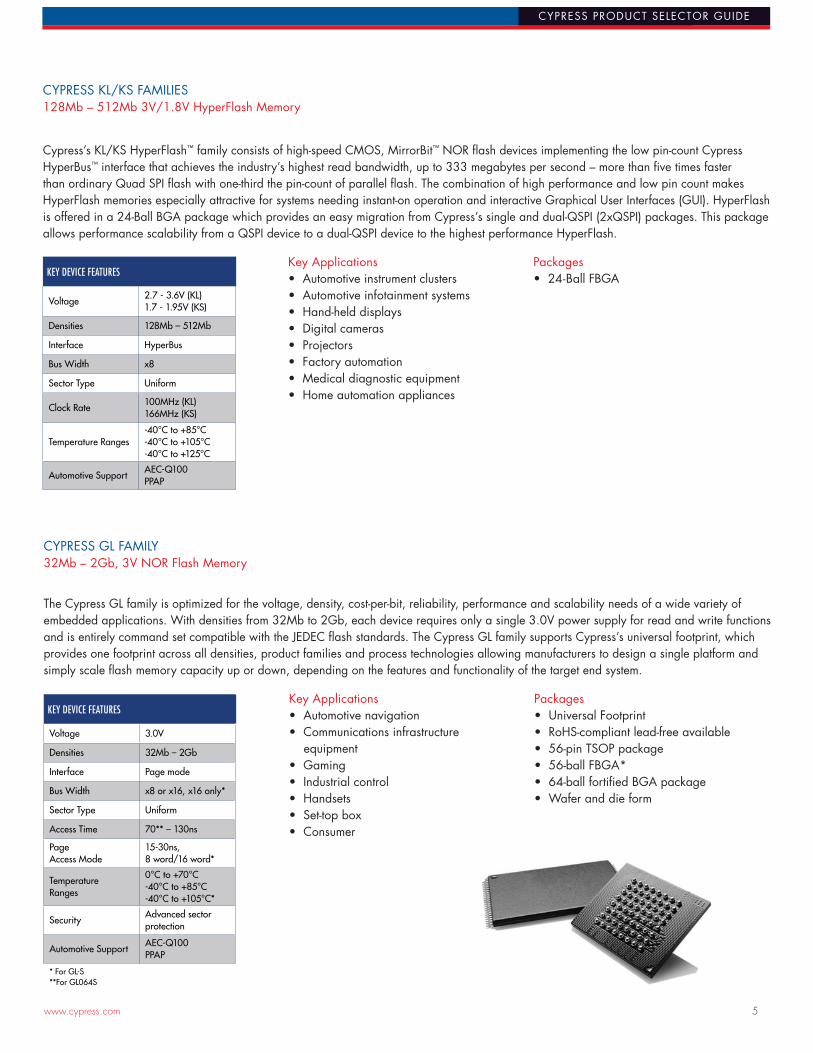
CYPRESS KL/KS FAMILIES128Mb – 512Mb 3V/1.8V HyperFlash Memory
Cypress’s KL/KS HyperFlash™ family consists of high-speed CMOS, MirrorBit™ NOR flash devices implementing the low pin-count Cypress HyperBus™ interface that achieves the industry’s highest read bandwidth, up to 333 megabytes per second – more than five times faster than ordinary Quad SPI flash with one-third the pin-count of parallel flash. The combination of high performance and low pin count makes HyperFlash memories especially attractive for systems needing instant-on operation and interactive Graphical User Interfaces (GUI). HyperFlash is offered in a 24-Ball BGA package which provides an easy migration from Cypress’s single and dual-QSPI (2xQSPI) packages. This package allows performance scalability from a QSPI device to a dual-QSPI device to the highest performance HyperFlash.
Key Applications• Automotive instrument clusters• Automotive infotainment systems• Hand-held displays• Digital cameras• Projectors• Factory automation• Medical diagnostic equipment• Home automation appliances
Packages• 24-Ball FBGAKEY DEVICE FEATURES
Voltage2.7 - 3.6V (KL) 1.7 - 1.95V (KS)
Densities 128Mb – 512Mb
Interface HyperBus
Bus Width x8
Sector Type Uniform
Clock Rate100MHz (KL)166MHz (KS)
Temperature Ranges-40°C to +85°C-40°C to +105°C-40°C to +125°C
Automotive SupportAEC-Q100PPAP
CYPRESS GL FAMILY32Mb – 2Gb, 3V NOR Flash Memory
The Cypress GL family is optimized for the voltage, density, cost-per-bit, reliability, performance and scalability needs of a wide variety of embedded applications. With densities from 32Mb to 2Gb, each device requires only a single 3.0V power supply for read and write functions and is entirely command set compatible with the JEDEC flash standards. The Cypress GL family supports Cypress’s universal footprint, which provides one footprint across all densities, product families and process technologies allowing manufacturers to design a single platform and simply scale flash memory capacity up or down, depending on the features and functionality of the target end system.
Key Applications• Automotive navigation• Communications infrastructure equipment• Gaming• Industrial control• Handsets• Set-top box• Consumer
Packages• Universal Footprint• RoHS-compliant lead-free available• 56-pin TSOP package• 56-ball FBGA*• 64-ball fortified BGA package• Wafer and die form
KEY DEVICE FEATURES
Voltage 3.0V
Densities 32Mb – 2Gb
Interface Page mode
Bus Width x8 or x16, x16 only*
Sector Type Uniform
Access Time 70** – 130ns
Page Access Mode
15-30ns,8 word/16 word*
Temperature Ranges
0°C to +70°C-40°C to +85°C-40°C to +105°C*
SecurityAdvanced sectorprotection
Automotive SupportAEC-Q100PPAP
* For GL-S**For GL064S
www.cypress.com 6 www.cypress.com 7
CYPRESS PRODUCT SELECTOR GUIDE
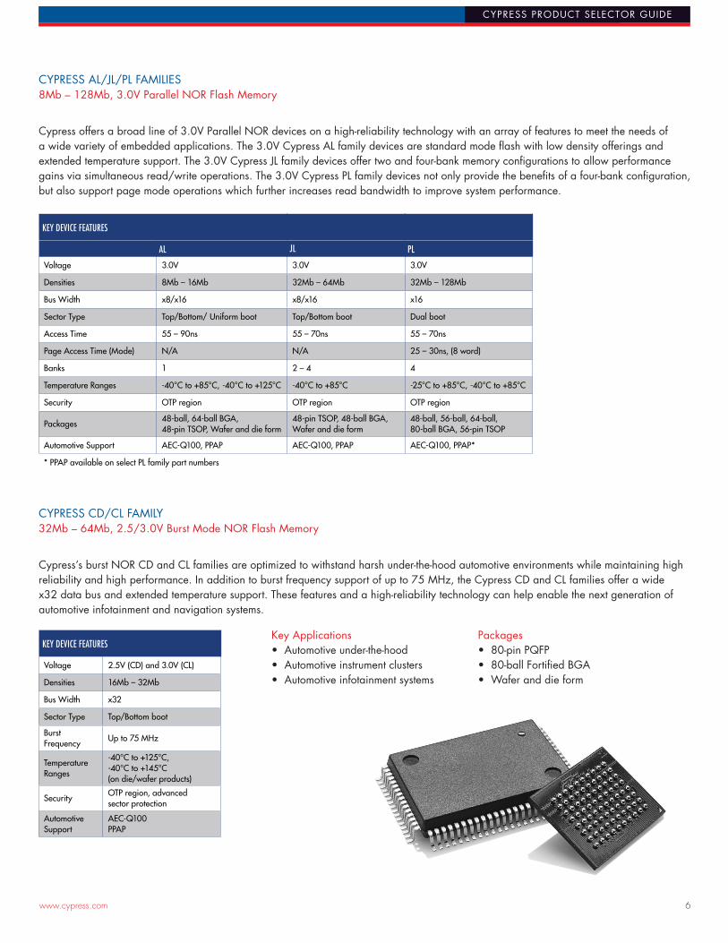
CYPRESS AL/JL/PL FAMILIES8Mb – 128Mb, 3.0V Parallel NOR Flash Memory
Cypress offers a broad line of 3.0V Parallel NOR devices on a high-reliability technology with an array of features to meet the needs of a wide variety of embedded applications. The 3.0V Cypress AL family devices are standard mode flash with low density offerings and extended temperature support. The 3.0V Cypress JL family devices offer two and four-bank memory configurations to allow performance gains via simultaneous read/write operations. The 3.0V Cypress PL family devices not only provide the benefits of a four-bank configuration, but also support page mode operations which further increases read bandwidth to improve system performance.
KEY DEVICE FEATURES
AL JL PL
Voltage 3.0V 3.0V 3.0V
Densities 8Mb – 16Mb 32Mb – 64Mb 32Mb – 128Mb
Bus Width x8/x16 x8/x16 x16
Sector Type Top/Bottom/ Uniform boot Top/Bottom boot Dual boot
Access Time 55 – 90ns 55 – 70ns 55 – 70ns
Page Access Time (Mode) N/A N/A 25 – 30ns, (8 word)
Banks 1 2 – 4 4
Temperature Ranges -40°C to +85°C, -40°C to +125°C -40°C to +85°C -25°C to +85°C, -40°C to +85°C
Security OTP region OTP region OTP region
Packages48-ball, 64-ball BGA, 48-pin TSOP, Wafer and die form
48-pin TSOP, 48-ball BGA, Wafer and die form
48-ball, 56-ball, 64-ball, 80-ball BGA, 56-pin TSOP
Automotive Support AEC-Q100, PPAP AEC-Q100, PPAP AEC-Q100, PPAP*
* PPAP available on select PL family part numbers
CYPRESS CD/CL FAMILY32Mb – 64Mb, 2.5/3.0V Burst Mode NOR Flash Memory
Cypress’s burst NOR CD and CL families are optimized to withstand harsh under-the-hood automotive environments while maintaining high reliability and high performance. In addition to burst frequency support of up to 75 MHz, the Cypress CD and CL families offer a wide x32 data bus and extended temperature support. These features and a high-reliability technology can help enable the next generation of automotive infotainment and navigation systems.
Key Applications• Automotive under-the-hood• Automotive instrument clusters• Automotive infotainment systems
Packages• 80-pin PQFP• 80-ball Fortified BGA• Wafer and die form
KEY DEVICE FEATURES
Voltage 2.5V (CD) and 3.0V (CL)
Densities 16Mb – 32Mb
Bus Width x32
Sector Type Top/Bottom boot
BurstFrequency
Up to 75 MHz
TemperatureRanges
-40°C to +125°C,-40°C to +145°C(on die/wafer products)
SecurityOTP region, advanced sector protection
Automotive Support
AEC-Q100PPAP
www.cypress.com 6 www.cypress.com 7
CYPRESS PRODUCT SELECTOR GUIDE
CYPRESS AS FAMILY8Mb – 16Mb, 1.8V NOR Flash Memory
The 1.8V Cypress AS family is optimized for performance and reliability. In addition to a fast initial access time of 70ns, the AS family offers low power consumption and a fast program speed which is ideal for a wide variety of embedded applications. Based on a proven 110nm Floating Gate process technology, the reliability of the AS family also makes it suitable for use in automotive-grade applications.
Key Applications• Handheld navigation• Bluetooth• Personal media players
Packages• 48-pin TSOP• 48-ball BGA (0.8mm pitch)• 48-ball BGA (0.5mm pitch)• Wafer and die form
KEY DEVICE FEATURES
Voltage 1.8V
Densities 8Mb - 16Mb
Interface Standard NOR
Bus Width x8/x16
Sector Type Top/Bottom boot
Access Time 70ns
Temperature Ranges
-40°C to +85°C-40°C to +105°C (16Mb)
Security
Secured Silicon Region, 256-byte OTP sector for permanent, secure identification
Automotive Support AEC-Q100
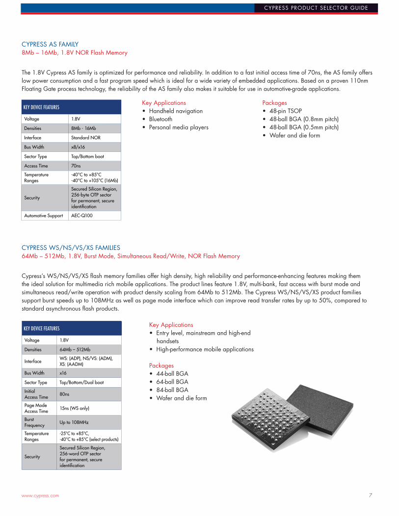
CYPRESS WS/NS/VS/XS FAMILIES64Mb – 512Mb, 1.8V, Burst Mode, Simultaneous Read/Write, NOR Flash Memory
Cypress’s WS/NS/VS/XS flash memory families offer high density, high reliability and performance-enhancing features making them the ideal solution for multimedia rich mobile applications. The product lines feature 1.8V, multi-bank, fast access with burst mode and simultaneous read/write operation with product density scaling from 64Mb to 512Mb. The Cypress WS/NS/VS/XS product families support burst speeds up to 108MHz as well as page mode interface which can improve read transfer rates by up to 50%, compared to standard asynchronous flash products.
Key Applications• Entry level, mainstream and high-end handsets• High-performance mobile applications
Packages• 44-ball BGA• 64-ball BGA • 84-ball BGA• Wafer and die form
KEY DEVICE FEATURES
Voltage 1.8V
Densities 64Mb – 512Mb
InterfaceWS: (ADP), NS/VS: (ADM), XS: (AADM)
Bus Width x16
Sector Type Top/Bottom/Dual boot
Initial Access Time
80ns
Page Mode Access Time
15ns (WS only)
BurstFrequency
Up to 108MHz
TemperatureRanges
-25°C to +85°C, -40°C to +85°C (select products)
Security
Secured Silicon Region, 256-word OTP sector for permanent, secure identification
www.cypress.com 8 www.cypress.com 9
CYPRESS PRODUCT SELECTOR GUIDE
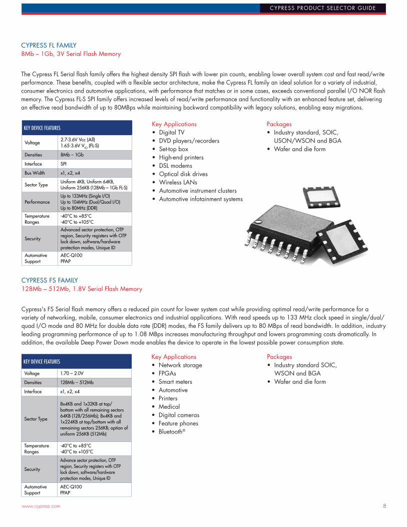
CYPRESS FL FAMILY8Mb – 1Gb, 3V Serial Flash Memory
The Cypress FL Serial flash family offers the highest density SPI flash with lower pin counts, enabling lower overall system cost and fast read/write performance. These benefits, coupled with a flexible sector architecture, make the Cypress FL family an ideal solution for a variety of industrial, consumer electronics and automotive applications, with performance that matches or in some cases, exceeds conventional parallel I/O NOR flash memory. The Cypress FL-S SPI family offers increased levels of read/write performance and functionality with an enhanced feature set, delivering an effective read bandwidth of up to 80MBps while maintaining backward compatibility with legacy solutions, enabling easy migrations.
Key Applications• Digital TV• DVD players/recorders• Set-top box• High-end printers• DSL modems• Optical disk drives• Wireless LANs• Automotive instrument clusters• Automotive infotainment systems
Packages• Industry standard, SOIC, USON/WSON and BGA• Wafer and die form
KEY DEVICE FEATURES
Voltage2.7-3.6V Vcc (All)1.65-3.6V VIO (FL-S)
Densities 8Mb – 1Gb
Interface SPI
Bus Width x1, x2, x4
Sector TypeUniform 4KB, Uniform 64KB, Uniform 256KB (128Mb – 1Gb FL-S)
PerformanceUp to 133MHz (Single I/O)Up to 104MHz (Dual/Quad I/O) Up to 80MHz (DDR)
Temperature Ranges
-40°C to +85°C-40°C to +105°C
Security
Advanced sector protection, OTP region, Security registers with OTP lock down, software/hardware protection modes, Unique ID
Automotive Support
AEC-Q100PPAP
CYPRESS FS FAMILY128Mb – 512Mb, 1.8V Serial Flash Memory
Cypress's FS Serial flash memory offers a reduced pin count for lower system cost while providing optimal read/write performance for a variety of networking, mobile, consumer electronics and industrial applications. With read speeds up to 133 MHz clock speed in single/dual/quad I/O mode and 80 MHz for double data rate (DDR) modes, the FS family delivers up to 80 MBps of read bandwidth. In addition, industry leading programming performance of up to 1.08 MBps increases manufacturing throughput and lowers programming costs dramatically. In addition, the available Deep Power Down mode enables the device to operate in the lowest possible power consumption state.
Key Applications• Network storage• FPGAs• Smart meters• Automotive• Printers• Medical• Digital cameras• Feature phones• Bluetooth®
Packages• Industry standard SOIC, WSON and BGA• Wafer and die form
KEY DEVICE FEATURES
Voltage 1.70 – 2.0V
Densities 128Mb – 512Mb
Interface x1, x2, x4
Sector Type
8x4KB and 1x32KB at top/bottom with all remaining sectors 64KB (128/256Mb); 8x4KB and 1x224KB at top/bottom with all remaining sectors 256KB; option of uniform 256KB (512Mb)
Temperature Ranges
-40°C to +85°C-40°C to +105°C
Security
Advance sector protection, OTP region, Security registers with OTP lock down, software/hardware protection modes, Unique ID
Automotive Support
AEC-Q100PPAP
www.cypress.com 8 www.cypress.com 9
CYPRESS PRODUCT SELECTOR GUIDE
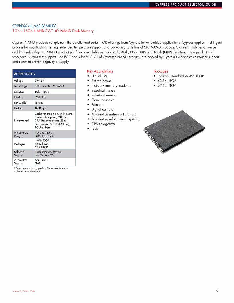
CYPRESS ML/MS FAMILIES1Gb – 16Gb NAND 3V/1.8V NAND Flash Memory
Cypress NAND products complement the parallel and serial NOR offerings from Cypress for embedded applications. Cypress applies its stringent process for qualification, testing, extended temperature support and packaging to its line of SLC NAND products. Cypress’s high performance and high reliability SLC NAND product portfolio is available in 1Gb, 2Gb, 4Gb, 8Gb (DDP) and 16Gb (QDP) densities. These products will work with systems that support 1-bit ECC and 4-bit ECC. All of Cypress’s NAND products are backed by Cypress’s world-class customer support and commitment for longevity of supply.
Key Applications• Digital TVs• Set-top boxes• Network memory modules• Industrial meters• Industrial sensors• Game consoles• Printers• Digital camera• Automotive instrument clusters• Automotive infotainment systems• GPS navigation• Toys
Packages• Industry Standard 48-Pin TSOP • 63-Ball BGA• 67-Ball BGA
KEY DEVICE FEATURES
Voltage 3V/1.8V
Technology 4x/3x nm SLC FG NAND
Densities 1Gb – 16Gb
Interface ONFI 1.0
Bus Width x8/x16
Cycling 100K (typ.)
Performance1
Cache Programming, Multi-plane commands support, OTP, and 25uS Random access, 25 ns Seq. access, 200-300uS tprog, 2-3.5ms tbers
TemperatureRanges
-40°C to +85°C,-40°C to +105°C
Packages48-Pin TSOP63-Ball BGA 67-Ball BGA
Software Support
Complimentary Drivers and Cypress FFS
Automotive Support
AEC-Q100PPAP
1 Performance varies by product. Please refer to product tables for more information.
www.cypress.com 10 www.cypress.com 11
CYPRESS PRODUCT SELECTOR GUIDE
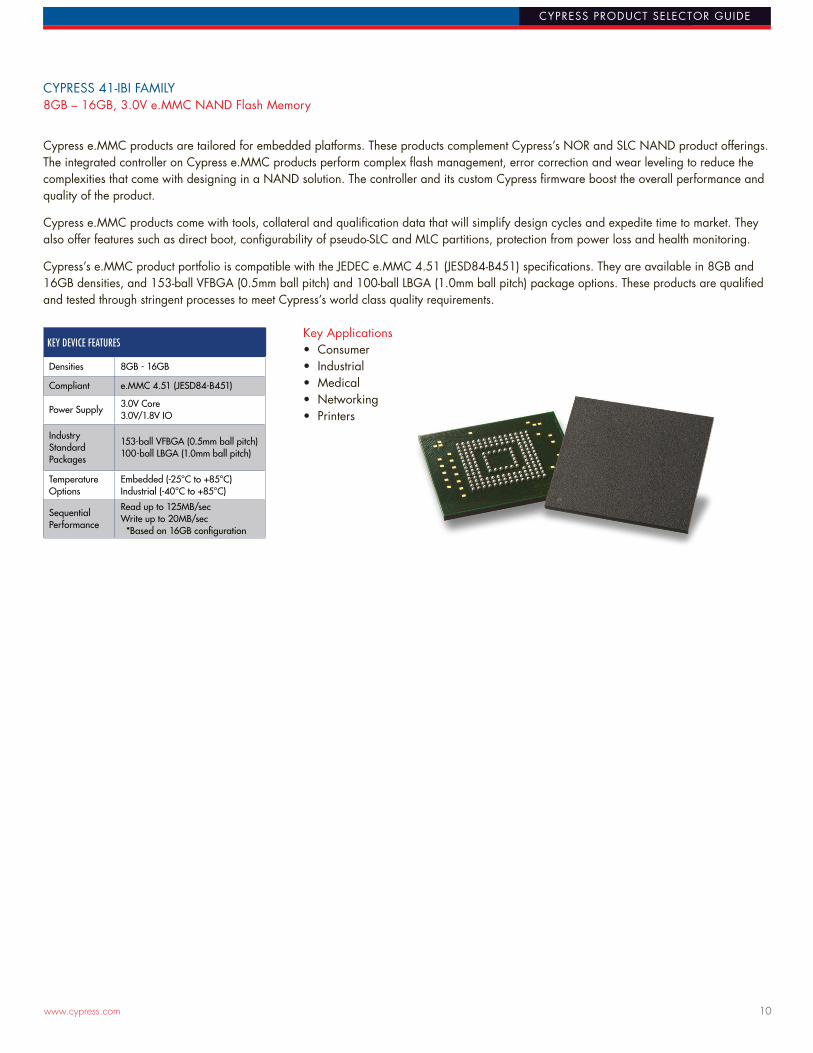
CYPRESS 41-IBI FAMILY8GB – 16GB, 3.0V e.MMC NAND Flash Memory
Cypress e.MMC products are tailored for embedded platforms. These products complement Cypress’s NOR and SLC NAND product offerings. The integrated controller on Cypress e.MMC products perform complex flash management, error correction and wear leveling to reduce the complexities that come with designing in a NAND solution. The controller and its custom Cypress firmware boost the overall performance and quality of the product.
Cypress e.MMC products come with tools, collateral and qualification data that will simplify design cycles and expedite time to market. They also offer features such as direct boot, configurability of pseudo-SLC and MLC partitions, protection from power loss and health monitoring.
Cypress’s e.MMC product portfolio is compatible with the JEDEC e.MMC 4.51 (JESD84-B451) specifications. They are available in 8GB and 16GB densities, and 153-ball VFBGA (0.5mm ball pitch) and 100-ball LBGA (1.0mm ball pitch) package options. These products are qualified and tested through stringent processes to meet Cypress’s world class quality requirements.
Key Applications• Consumer• Industrial• Medical• Networking• Printers
KEY DEVICE FEATURES
Densities 8GB - 16GB
Compliant e.MMC 4.51 (JESD84-B451)
Power Supply3.0V Core 3.0V/1.8V IO
Industry Standard Packages
153-ball VFBGA (0.5mm ball pitch) 100-ball LBGA (1.0mm ball pitch)
Temperature Options
Embedded (-25°C to +85°C)Industrial (-40°C to +85°C)
Sequential Performance
Read up to 125MB/sec Write up to 20MB/sec *Based on 16GB configuration
www.cypress.com 10 www.cypress.com 11
CYPRESS PRODUCT SELECTOR GUIDE
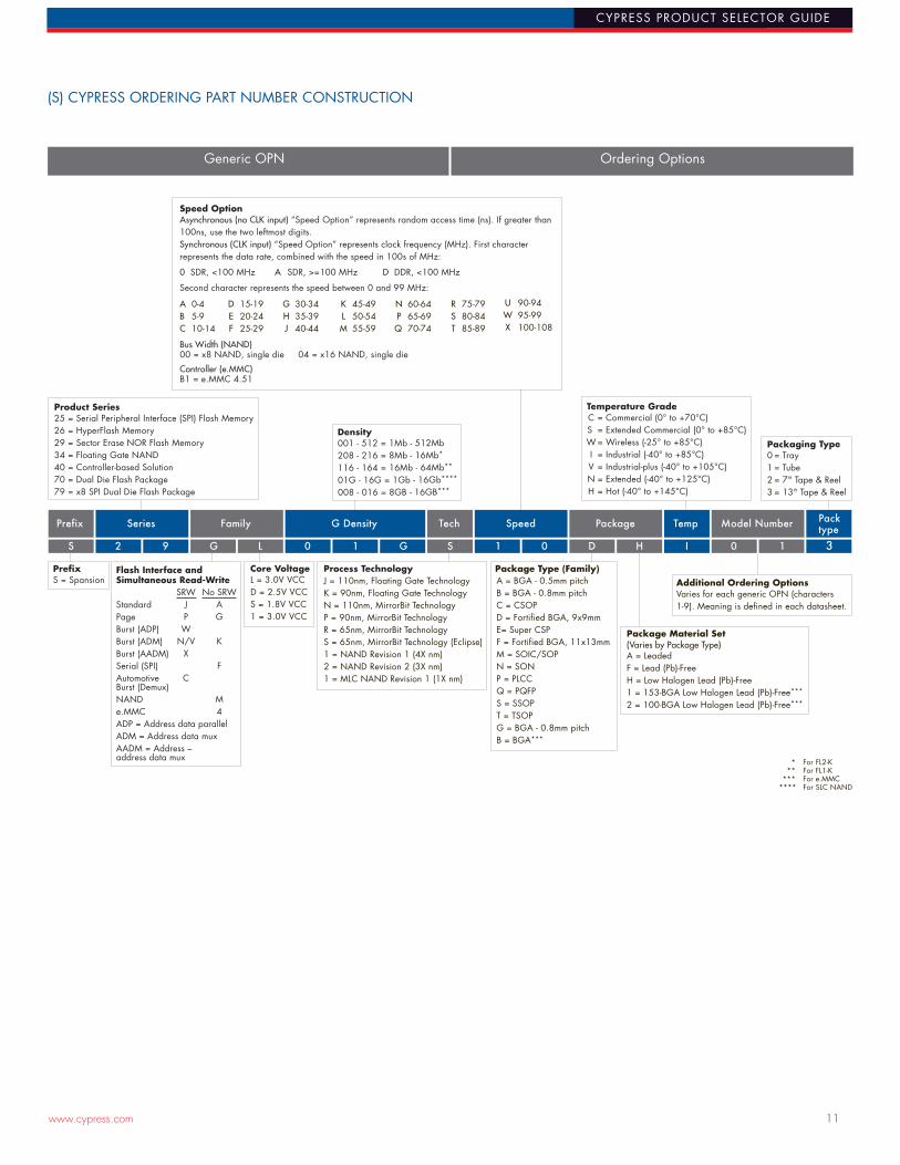
(S) CYPRESS ORDERING PART NUMBER CONSTRUCTION
Generic OPN Ordering Options
Additional Ordering OptionsVaries for each generic OPN (characters1-9). Meaning is defined in each datasheet.
Prefix Series Family G Density Tech Speed Package Temp Model Number Pack type
S S 1 0 D H I2 9 G L 0 1 G 0 1 3
Temperature GradeProduct Series25 = Serial Peripheral Interface (SPI) Flash Memory26 = HyperFlash Memory29 = Sector Erase NOR Flash Memory34 = Floating Gate NAND40 = Controller-based Solution70 = Dual Die Flash Package79 = x8 SPI Dual Die Flash Package
Density001 - 512 = 1Mb - 512Mb208 - 216 = 8Mb - 16Mb*
116 - 164 = 16Mb - 64Mb**
01G - 16G = 1Gb - 16Gb****
008 - 016 = 8GB - 16GB***
Packaging Type
PrefixS = Spansion
Package Type (Family)
Package Material Set (Varies by Package Type)
Process TechnologyFlash Interface andSimultaneous Read-Write
StandardPageBurst (ADP)Burst (ADM) Burst (AADM)Serial (SPI)AutomotiveBurst (Demux)NANDe.MMCADP = Address data parallelADM = Address data muxAADM = Address –address data mux
SRWJPW
N/VX
C
No SRWAG
K
F
M4
CS WIVNH
= Commercial (0° to +70°C)= Extended Commercial (0° to +85°C)= Wireless (-25° to +85°C)= Industrial (-40° to +85°C)= Industrial-plus (-40° to +105°C)= Extended (-40° to +125°C)= Hot (-40° to +145°C)
0123
= Tray= Tube= 7" Tape & Reel= 13" Tape & Reel
* For FL2-K ** For FL1-K *** For e.MMC**** For SLC NAND
Speed OptionAsynchronous (no CLK input) “Speed Option” represents random access time (ns). If greater than 100ns, use the two leftmost digits. Synchronous (CLK input) “Speed Option” represents clock frequency (MHz). First characterrepresents the data rate, combined with the speed in 100s of MHz:
0 SDR, <100 MHz A SDR, >=100 MHz D DDR, <100 MHz
Second character represents the speed between 0 and 99 MHz:
0-45-910-14
15-1920-2425-29
30-3435-3940-44
45-4950-5455-59
60-6465-6970-74
75-7980-8485-89
90-9495-99100-108
ABC
DEF
GHJ
KLM
NPQ
RST
UWX
Bus Width (NAND)00 = x8 NAND, single die 04 = x16 NAND, single die
Controller (e.MMC)B1 = e.MMC 4.51
Core VoltageL = 3.0V VCCD = 2.5V VCCS = 1.8V VCC1 = 3.0V VCC
J = 110nm, Floating Gate TechnologyK = 90nm, Floating Gate TechnologyN = 110nm, MirrorBit TechnologyP = 90nm, MirrorBit TechnologyR = 65nm, MirrorBit TechnologyS = 65nm, MirrorBit Technology (Eclipse)1 = NAND Revision 1 (4X nm)2 = NAND Revision 2 (3X nm)1 = MLC NAND Revision 1 (1X nm)
A = BGA - 0.5mm pitchB = BGA - 0.8mm pitchC = CSOPD = Fortified BGA, 9x9mmE= Super CSPF = Fortified BGA, 11x13mmM = SOIC/SOPN = SONP = PLCCQ = PQFPS = SSOPT = TSOPG = BGA - 0.8mm pitchB = BGA***
A = LeadedF = Lead (Pb)-FreeH = Low Halogen Lead (Pb)-Free1 = 153-BGA Low Halogen Lead (Pb)-Free***
2 = 100-BGA Low Halogen Lead (Pb)-Free***
www.cypress.com 12 www.cypress.com 13
CYPRESS PRODUCT SELECTOR GUIDE
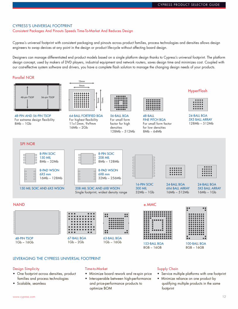
CYPRESS’S UNIVERSAL FOOTPRINTConsistent Packages And Pinouts Speeds Time-To-Market And Reduces Design
Cypress’s universal footprint with consistent packaging and pinouts across product families, process technologies and densities allows design engineers to swap devices at any point in the design or product life-cycle without affecting board design.
Designers can manage differentiated end product models based on a single platform design thanks to Cypress’s universal footprint. The platform design concept, used by makers of DVD players, industrial equipment and network routers, saves design time and minimizes cost. Coupled with our cost-effective system software and drivers, you have a complete flash solution to manage the changing design needs of your products.
150 MIL SOIC AND 6X5 WSON
8-PIN SOIC 150 MIL 8Mb – 32Mb
8-PAD WSON 6X5 mm16Mb – 128Mb
208 MIL SOIC AND 6X8 WSONSingle footprint, widest density range
8-PIN SOIC 208 MIL 8Mb – 128Mb
8-PAD WSON 6X8 mm32Mb – 256Mb
SPI NOR
16-PIN SOIC 300 MIL32Mb – 1Gb
24-BALL BGA6X4 BALL ARRAY16Mb – 512Mb
24-BALL BGA5X5 BALL ARRAY16Mb – 1Gb
64-BALL FORTIFIED BGAFor highest flexibility11x13mm, 9x9mm16Mb – 2Gb
13mm
9mm
9mm
11m
m
48-pin TSOP 56-pin TSOP
56-BALL BGAFor small form factor for high densities128Mb – 512Mb
13mm
9mm
9mm
11m
m
48-pin TSOP 56-pin TSOP
48-PIN AND 56-PIN TSOPFor extreme design flexibility8Mb – 1Gb
13mm
9mm
9mm
11m
m
48-pin TSOP 56-pin TSOP
Parallel NOR
48-BALLFINE PITCH BGAFor small form factor for low densities8Mb – 64Mb
13mm
9mm
9mm
11m
m
48-pin TSOP 56-pin TSOP
HyperFlash
24-BALL BGA5X5 BALL ARRAY128Mb – 512Mb
NAND
48-PIN TSOP1Gb – 16Gb
63-BALL BGA1Gb – 16Gb
67-BALL BGA1Gb – 2Gb
e.MMC
153-BALL BGA8GB – 16GB
100-BALL BGA8GB – 16GB
LEVERAGING THE CYPRESS UNIVERSAL FOOTPRINT
Design Simplicity• One footprint across densities, product
families and process technologies• Scalable, seamless
Time-to-Market• Minimize board rework and re-spin price• Interoperable between high-performance
and price-performance products to optimize BOM
Supply Chain• Service multiple platforms with one footprint• Minimize reliance on one product by
qualifying multiple products in the same footprint
www.cypress.com 12 www.cypress.com 13
CYPRESS PRODUCT SELECTOR GUIDE
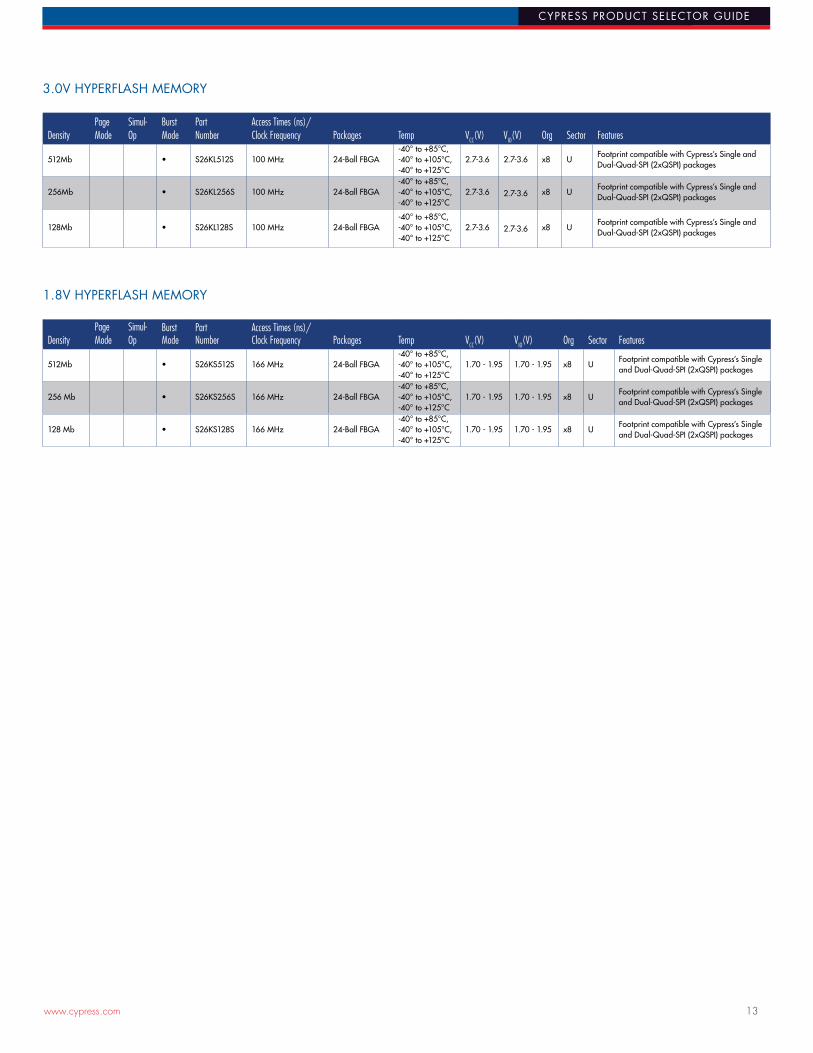
3.0V HYPERFLASH MEMORY
DensityPage Mode
Simul-Op
Burst Mode
Part Number
Access Times (ns)/ Clock Frequency Packages Temp VCC(V) VIO(V) Org Sector Features
512Mb • S26KL512S 100 MHz 24-Ball FBGA-40° to +85°C, -40° to +105°C,-40° to +125°C
2.7-3.6 2.7-3.6 x8 UFootprint compatible with Cypress’s Single and Dual-Quad-SPI (2xQSPI) packages
256Mb • S26KL256S 100 MHz 24-Ball FBGA-40° to +85°C, -40° to +105°C,-40° to +125°C
2.7-3.6 2.7-3.6 x8 UFootprint compatible with Cypress’s Single and Dual-Quad-SPI (2xQSPI) packages
128Mb • S26KL128S 100 MHz 24-Ball FBGA-40° to +85°C, -40° to +105°C,-40° to +125°C
2.7-3.6 2.7-3.6 x8 UFootprint compatible with Cypress’s Single and Dual-Quad-SPI (2xQSPI) packages
DensityPage Mode
Simul-Op
Burst Mode
Part Number
Access Times (ns)/ Clock Frequency Packages Temp VCC(V) VIO(V) Org Sector Features
512Mb • S26KS512S 166 MHz 24-Ball FBGA-40° to +85°C, -40° to +105°C,-40° to +125°C
1.70 - 1.95 1.70 - 1.95 x8 UFootprint compatible with Cypress’s Single and Dual-Quad-SPI (2xQSPI) packages
256 Mb • S26KS256S 166 MHz 24-Ball FBGA-40° to +85°C, -40° to +105°C,-40° to +125°C
1.70 - 1.95 1.70 - 1.95 x8 UFootprint compatible with Cypress’s Single and Dual-Quad-SPI (2xQSPI) packages
128 Mb • S26KS128S 166 MHz 24-Ball FBGA-40° to +85°C, -40° to +105°C,-40° to +125°C
1.70 - 1.95 1.70 - 1.95 x8 UFootprint compatible with Cypress’s Single and Dual-Quad-SPI (2xQSPI) packages
1.8V HYPERFLASH MEMORY
www.cypress.com 14 www.cypress.com 15
CYPRESS PRODUCT SELECTOR GUIDE
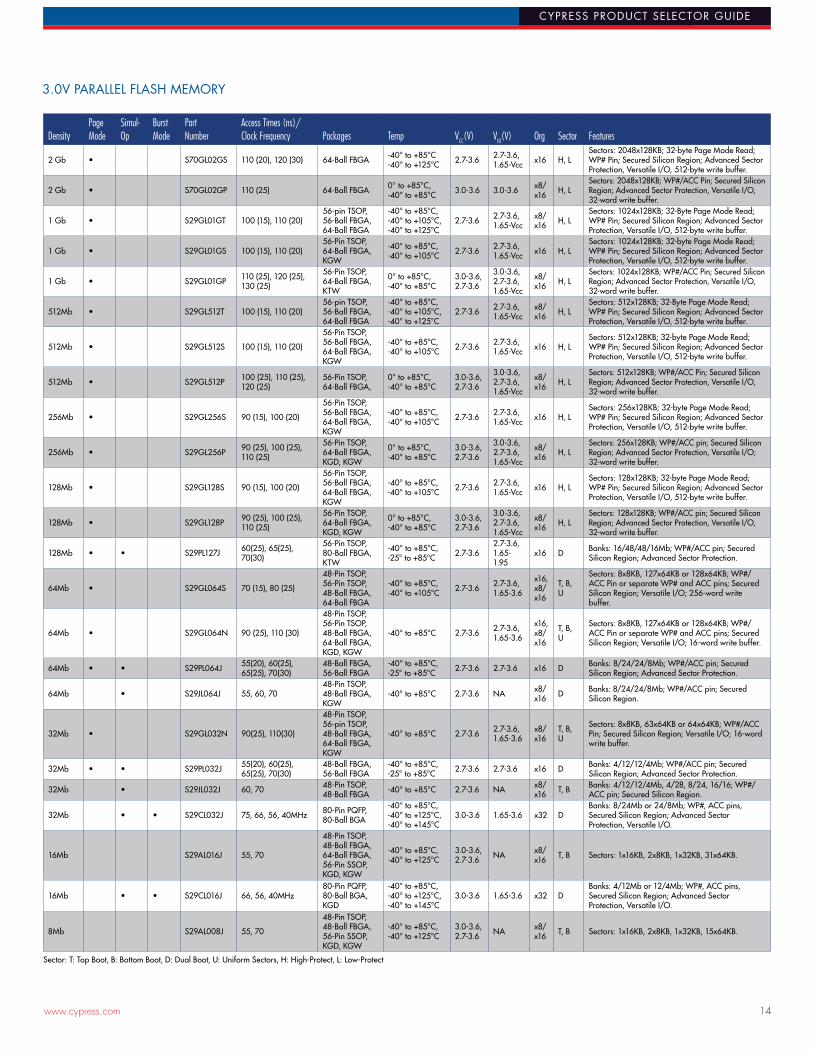
3.0V PARALLEL FLASH MEMORY
DensityPage Mode
Simul-Op
Burst Mode
Part Number
Access Times (ns)/ Clock Frequency Packages Temp VCC(V) VIO(V) Org Sector Features
2 Gb • S70GL02GS 110 (20), 120 (30) 64-Ball FBGA -40° to +85°C -40° to +125°C 2.7-3.6 2.7-3.6,
1.65-Vcc x16 H, LSectors: 2048x128KB; 32-byte Page Mode Read; WP# Pin; Secured Silicon Region; Advanced Sector Protection, Versatile I/O, 512-byte write buffer.
2 Gb • S70GL02GP 110 (25) 64-Ball FBGA 0° to +85°C, -40° to +85°C 3.0-3.6 3.0-3.6 x8/
x16 H, LSectors: 2048x128KB; WP#/ACC Pin; Secured Silicon Region; Advanced Sector Protection, Versatile I/O, 32-word write buffer.
1 Gb • S29GL01GT 100 (15), 110 (20)56-pin TSOP, 56-Ball FBGA, 64-Ball FBGA
-40° to +85°C,-40° to +105°C,-40° to +125°C
2.7-3.6 2.7-3.6, 1.65-Vcc
x8/x16 H, L
Sectors: 1024x128KB; 32-Byte Page Mode Read; WP# Pin; Secured Silicon Region; Advanced Sector Protection, Versatile I/O, 512-byte write buffer.
1 Gb • S29GL01GS 100 (15), 110 (20)56-Pin TSOP, 64-Ball FBGA, KGW
-40° to +85°C, -40° to +105°C 2.7-3.6 2.7-3.6,
1.65-Vcc x16 H, LSectors: 1024x128KB; 32-byte Page Mode Read; WP# Pin; Secured Silicon Region; Advanced Sector Protection, Versatile I/O, 512-byte write buffer.
1 Gb • S29GL01GP 110 (25), 120 (25), 130 (25)
56-Pin TSOP, 64-Ball FBGA, KTW
0° to +85°C, -40° to +85°C
3.0-3.6, 2.7-3.6
3.0-3.6, 2.7-3.6, 1.65-Vcc
x8/x16 H, L
Sectors: 1024x128KB; WP#/ACC Pin; Secured Silicon Region; Advanced Sector Protection, Versatile I/O, 32-word write buffer.
512Mb • S29GL512T 100 (15), 110 (20)56-pin TSOP, 56-Ball FBGA, 64-Ball FBGA
-40° to +85°C,-40° to +105°C,-40° to +125°C
2.7-3.6 2.7-3.6, 1.65-Vcc
x8/x16 H, L
Sectors: 512x128KB; 32-Byte Page Mode Read; WP# Pin; Secured Silicon Region; Advanced Sector Protection, Versatile I/O, 512-byte write buffer.
512Mb • S29GL512S 100 (15), 110 (20)
56-Pin TSOP, 56-Ball FBGA, 64-Ball FBGA, KGW
-40° to +85°C, -40° to +105°C 2.7-3.6 2.7-3.6,
1.65-Vcc x16 H, LSectors: 512x128KB; 32-byte Page Mode Read; WP# Pin; Secured Silicon Region; Advanced Sector Protection, Versatile I/O, 512-byte write buffer.
512Mb • S29GL512P 100 (25), 110 (25), 120 (25)
56-Pin TSOP, 64-Ball FBGA,
0° to +85°C, -40° to +85°C
3.0-3.6, 2.7-3.6
3.0-3.6, 2.7-3.6, 1.65-Vcc
x8/x16 H, L
Sectors: 512x128KB; WP#/ACC Pin; Secured Silicon Region; Advanced Sector Protection, Versatile I/O, 32-word write buffer.
256Mb • S29GL256S 90 (15), 100 (20)
56-Pin TSOP, 56-Ball FBGA, 64-Ball FBGA, KGW
-40° to +85°C, -40° to +105°C 2.7-3.6 2.7-3.6,
1.65-Vcc x16 H, LSectors: 256x128KB; 32-byte Page Mode Read; WP# Pin; Secured Silicon Region; Advanced Sector Protection, Versatile I/O, 512-byte write buffer.
256Mb • S29GL256P 90 (25), 100 (25), 110 (25)
56-Pin TSOP, 64-Ball FBGA, KGD, KGW
0° to +85°C, -40° to +85°C
3.0-3.6, 2.7-3.6
3.0-3.6, 2.7-3.6, 1.65-Vcc
x8/x16 H, L
Sectors: 256x128KB; WP#/ACC pin; Secured Silicon Region; Advanced Sector Protection, Versatile I/O; 32-word write buffer.
128Mb • S29GL128S 90 (15), 100 (20)
56-Pin TSOP, 56-Ball FBGA, 64-Ball FBGA, KGW
-40° to +85°C, -40° to +105°C 2.7-3.6 2.7-3.6,
1.65-Vcc x16 H, LSectors: 128x128KB; 32-byte Page Mode Read; WP# Pin; Secured Silicon Region; Advanced Sector Protection, Versatile I/O, 512-byte write buffer.
128Mb • S29GL128P 90 (25), 100 (25), 110 (25)
56-Pin TSOP, 64-Ball FBGA, KGD, KGW
0° to +85°C, -40° to +85°C
3.0-3.6, 2.7-3.6
3.0-3.6, 2.7-3.6, 1.65-Vcc
x8/x16 H, L
Sectors: 128x128KB; WP#/ACC pin; Secured Silicon Region; Advanced Sector Protection, Versatile I/O, 32-word write buffer.
128Mb • • S29PL127J 60(25), 65(25), 70(30)
56-Pin TSOP, 80-Ball FBGA, KTW
-40° to +85°C, -25° to +85°C 2.7-3.6
2.7-3.6, 1.65-1.95
x16 D Banks: 16/48/48/16Mb; WP#/ACC pin; Secured Silicon Region; Advanced Sector Protection.
64Mb • S29GL064S 70 (15), 80 (25)
48-Pin TSOP, 56-Pin TSOP, 48-Ball FBGA, 64-Ball FBGA
-40° to +85°C, -40° to +105°C 2.7-3.6 2.7-3.6,
1.65-3.6
x16, x8/x16
T, B, U
Sectors: 8x8KB, 127x64KB or 128x64KB; WP#/ACC Pin or separate WP# and ACC pins; Secured Silicon Region; Versatile I/O; 256-word write buffer.
64Mb • S29GL064N 90 (25), 110 (30)
48-Pin TSOP, 56-Pin TSOP, 48-Ball FBGA, 64-Ball FBGA, KGD, KGW
-40° to +85°C 2.7-3.6 2.7-3.6, 1.65-3.6
x16, x8/x16
T, B, U
Sectors: 8x8KB, 127x64KB or 128x64KB; WP#/ACC Pin or separate WP# and ACC pins; Secured Silicon Region; Versatile I/O; 16-word write buffer.
64Mb • • S29PL064J 55(20), 60(25), 65(25), 70(30)
48-Ball FBGA, 56-Ball FBGA
-40° to +85°C, -25° to +85°C 2.7-3.6 2.7-3.6 x16 D Banks: 8/24/24/8Mb; WP#/ACC pin; Secured
Silicon Region; Advanced Sector Protection.
64Mb • S29JL064J 55, 60, 7048-Pin TSOP, 48-Ball FBGA, KGW
-40° to +85°C 2.7-3.6 NA x8/x16 D Banks: 8/24/24/8Mb; WP#/ACC pin; Secured
Silicon Region.
32Mb • S29GL032N 90(25), 110(30)
48-Pin TSOP, 56-pin TSOP, 48-Ball FBGA, 64-Ball FBGA, KGW
-40° to +85°C 2.7-3.6 2.7-3.6, 1.65-3.6
x8/x16
T, B, U
Sectors: 8x8KB, 63x64KB or 64x64KB; WP#/ACC Pin; Secured Silicon Region; Versatile I/O; 16-word write buffer.
32Mb • • S29PL032J 55(20), 60(25), 65(25), 70(30)
48-Ball FBGA, 56-Ball FBGA
-40° to +85°C, -25° to +85°C 2.7-3.6 2.7-3.6 x16 D Banks: 4/12/12/4Mb; WP#/ACC pin; Secured
Silicon Region; Advanced Sector Protection.
32Mb • S29JL032J 60, 70 48-Pin TSOP, 48-Ball FBGA -40° to +85°C 2.7-3.6 NA x8/
x16 T, B Banks: 4/12/12/4Mb, 4/28, 8/24, 16/16; WP#/ACC pin; Secured Silicon Region.
32Mb • • S29CL032J 75, 66, 56, 40MHz 80-Pin PQFP, 80-Ball BGA
-40° to +85°C, -40° to +125°C, -40° to +145°C
3.0-3.6 1.65-3.6 x32 DBanks: 8/24Mb or 24/8Mb; WP#, ACC pins, Secured Silicon Region; Advanced Sector Protection, Versatile I/O.
16Mb S29AL016J 55, 70
48-Pin TSOP, 48-Ball FBGA, 64-Ball FBGA, 56-Pin SSOP, KGD, KGW
-40° to +85°C, -40° to +125°C
3.0-3.6, 2.7-3.6 NA x8/
x16 T, B Sectors: 1x16KB, 2x8KB, 1x32KB, 31x64KB.
16Mb • • S29CL016J 66, 56, 40MHz80-Pin PQFP, 80-Ball BGA, KGD
-40° to +85°C, -40° to +125°C, -40° to +145°C
3.0-3.6 1.65-3.6 x32 DBanks: 4/12Mb or 12/4Mb; WP#, ACC pins, Secured Silicon Region; Advanced Sector Protection, Versatile I/O.
8Mb S29AL008J 55, 70
48-Pin TSOP, 48-Ball FBGA, 56-Pin SSOP, KGD, KGW
-40° to +85°C, -40° to +125°C
3.0-3.6, 2.7-3.6 NA x8/
x16 T, B Sectors: 1x16KB, 2x8KB, 1x32KB, 15x64KB.
Sector: T: Top Boot, B: Bottom Boot, D: Dual Boot, U: Uniform Sectors, H: High-Protect, L: Low-Protect
www.cypress.com 14 www.cypress.com 15
CYPRESS PRODUCT SELECTOR GUIDE
2.5V PARALLEL FLASH MEMORY
DensityPage Mode
Simul-Op
Burst Mode
Part Number
Access Times (ns)/Clock Frequency Packages Temp VCC(V) VI/O(V) Org Sector Features
32Mb • • S29CD032J 75, 66, 56, 40MHz80-Pin PQFP, 80-Ball BGA, KGD
-40° to +85°C, -40° to +125°C, -40° to +145°C
2.5-2.75 1.65-2.75 x32 DBanks: 8/24Mb or 24/8Mb; WP#, ACC pins, Secured Silicon Region; Advanced Sector Protection, Versatile I/O.
16Mb • • S29CD016J 66, 56, 40MHz80-Pin PQFP, 80-Ball BGA, KGD
-40° to +85°C, -40° to +125°C, -40° to +145°C
2.5-2.75 1.65-2.75 x32 DBanks: 4/12Mb or 12/4Mb; WP#, ACC pins, Secured Silicon Region; Advanced Sector Protection, Versatile I/O.
1.8V PARALLEL ADP FLASH MEMORY
DensityPage Mode
Simul-Op
Burst Mode
Part Number
Access Times (ns)/Clock Frequency Packages Temp VCC(V) VI/O(V) Org Sector Features
512Mb • • • S29WS512P54, 66, 80, 104MHz
84-Ball FBGA -25° to +85°C 1.70-1.95 1.70-1.95 x16 DBanks: 16x32Mb; WP#, ACC Pins; Secured Silicon Region; Advanced Sector Protection; 32-word write buffer.
256Mb • • • S29WS256P54, 66, 80, 104MHz
84-Ball FBGA -25° to +85°C 1.70-1.95 1.70-1.95 x16 DBanks: 16x16Mb; WP#, ACC Pins; Secured Silicon Region; Advanced Sector Protection; 32-word write buffer.
128Mb • • • S29WS128P54, 66, 80, 104MHz
84-Ball FBGA, KTD, KGW
-25° to +85°C 1.70-1.95 1.70-1.95 x16 DBanks: 16x8Mb; WP#, ACC Pins; Secured Silicon Region; Advanced Sector Protection; 32-word write buffer.
64Mb • • • S29WS064R66, 83, 108MHz
84-Ball FBGA-40° to +85°C, -25° to +25°C
1.70-1.95 1.70-1.95 x16 T, BBanks: 4x16Mb; ACC Pin; Secured Silicon Region; Advanced Sector Protection; 32-word write buffer.
16Mb S29AS016J 7048-Pin TSOP, 48-Ball FBGA, KGD, KGW
-40° to +85°C 1.65-1.95 NAx8/x16
T, B Sectors: 8x8KB, 31x64KB; WP# pin, RY/BY# pin.
8Mb S29AS008J 7048-Pin TSOP, 48-Ball FBGA, KGD, KGW
-40° to +85°C 1.65-1.95 NAx8/x16
T, B Sectors: 8x8KB, 15x64KB; WP# pin, RY/BY# pin.
1.8V MUXED AADM FLASH MEMORY
DensityPage Mode
Simul-Op
Burst Mode
Part Number
Access Times (ns)/Clock Frequency Packages Temp VCC(V) VI/O(V) Org Sector Features
256Mb • • S29XS256R83, 104, 108MHz
44-Ball FBGA-40° to +85°C, -25° to +85°C
1.70-1.95 1.70-1.95 x16 T, BBanks: 8x32Mb; WP#, ACC Pins; Secured Silicon Region; 32-word write buffer.
128Mb • • S29XS128R83, 104, 108MHz
44-Ball FBGA-40° to +85°C, -25° to +85°C
1.70-1.95 1.70-1.95 x16 T, BBanks: 8x16Mb; WP#, ACC Pins; Secured Silicon Region 32-word write buffer.
64Mb • • S29XS064R 66, 83, 108MHz 44-Ball FBGA-40° to +85°C, -25° to +85°C
1.70-1.95 1.70-1.95 x16 T, BBanks: 8x16Mb; WP#, ACC Pins; Secured Silicon Region; Advanced Sector Protection; 32-word write buffer.
1.8V MUXED ADM FLASH MEMORY
DensityPage Mode
Simul-Op
Burst Mode
Part Number
Access Times (ns)/Clock Frequency Packages Temp VCC(V) VI/O(V) Org Sector Features
512Mb • • S29NS512P 66, 83MHz 64-Ball BGA -25° to +85°C 1.70-1.95 1.70-1.95 x16 TBanks: 16x32Mb; WP#, ACC Pins; Secured Silicon Region; Advanced Sector Protection; 32-word write buffer.
256Mb • • S29VS256R 83, 104, 108MHz 44-Ball FBGA-40° to +85°C, -25° to +85°C
1.70-1.95 1.70-1.95 x16 T, BBanks: 8x32Mb; WP#, ACC Pins; Secured Silicon Region; 32-word write buffer.
128Mb • • S29VS128R 83, 104, 108MHz 44-Ball FBGA-40° to +85°C, -25° to +85°C
1.70-1.95 1.70-1.95 x16 T, BBanks: 8x16Mb; WP#, ACC Pins; Secured Silicon Region; 32-word write buffer.
64Mb • • S29VS064R 66, 83, 108MHz 44-Ball FBGA-40° to +85°C, -25° to +85°C
1.70-1.95 1.70-1.95 x16 T, BBanks: 4x16Mb; ACC Pin; Secured Silicon Region; Advanced Sector Protection; 32-word write buffer.
www.cypress.com 16 www.cypress.com 17
CYPRESS PRODUCT SELECTOR GUIDE
3.0V & 1.8V SPI FLASH MEMORY
DensityPage Mode
Simul-Op
Burst Mode
Part Number
Access Times (ns)/ Clock Frequency Packages Temp VCC(V) VIO(V) Org Sector Features
1 Gb S70FL01GS133MHz (Single I/O), 104MHz (Multi I/O), 80MHz (DDR)1
16-Pin SO, 24-ball BGA (6x8mm)
-40° to +85°C, -40° to +105°C
2.7-3.6x1, x2, x4
UDual Die stack; Sectors: uniform 256KB; H/W & S/W write protect; OTP sector.
512Mb S25FS512S33MHz (Single I/O), 104MHz (Multi I/O), 80MHz (DDR)
16-pin SO, 24-ball BGA (6x8 mm), WSON 6x8 mm
-40° to +85°C, -40° to +105°C
1.7-2.0x1, x2, x4
USectors: uniform 256KB with eight 4KB sub-sectors and one 224KB sub-sector top/bottom; or all uniform 256KB sectors.
512Mb S25FL512S133MHz (Single I/O), 104MHz (Multi I/O), 80MHz (DDR)1
16-Pin SO, 24-ball BGA (6x8mm)
-40° to +85°C, -40° to +105°C
2.7-3.6 1.65-3.6x1, x2, x4
USectors: uniform 256KB; H/W & S/W write protect; OTP sector.
256Mb S25FS256S133MHz (Single I/O, Multi I/O), 80MHz (DDR)
16-pin SO, 8-contact WSON (6x8mm), 24-ball BGA (6x8mm)
-40° to +85°C, -40° to +105°C
1.7-2.0x1, x2, x4
U
Sectors: uniform 256KB or uniform 64KB with eight 4KB sub-sectors and one 32KB sub-sector top/bottom, all remaining sectors 64KB; H/W & S/W write protect; OTP sector.
256Mb S25FL256S133MHz (Single I/O), 104MHz (Multi I/O), 80MHz (DDR)1
16-Pin SO, 8-contact WSON (6x8 mm), 24-ball BGA (6x8mm)
-40° to +85°C, -40° to +105°C
2.7-3.6 1.65-3.6x1, x2, x4
USectors: uniform 256KB or uniform 64KB with 32 top/bottom 4KB sub-sectors; H/W & S/W write protect; OTP sector.
256Mb S70FL256P104MHz (Single I/O), 80MHz (Multi I/O)
16-Pin SO, 24-ball BGA (6x8mm)
-40° to +85°C 2.7-3.6x1, x2, x4
USectors: uniform 256KB or uniform 64KB with 32 top/bottom 4KB sub-sectors; H/W & S/W write protect; OTP sector; ACC pin.
128Mb S25FS128S133MHz (Single I/O, Multi I/O), 80MHz (DDR)
8-pin SO 208mil, 8-contact WSON (6x5mm), 24-ball BGA (6x8mm)
-40° to +85°C, -40° to +105°C
1.7-2.0x1, x2, x4
U
Sectors: uniform 256KB or uniform 64KB with eight 4KB sub-sectors and one 32KB sub-sector top/bottom, all remaining sectors 64KB; H/W & S/W write protect; OTP sector.
128Mb S25FL127S108MHz (Single I/O), 108MHz (Multi I/O)
16-Pin SO, 8-pin SO 208mil, 8-contact WSON (6x5mm), 24-ball BGA (6x8mm)
-40° to +85°C, -40° to +105°C
2.7-3.6x1, x2, x4
USectors: uniform 256KB or uniform 64KB with 16 top/bottom 4KB sub-sectors; H/W & S/W write protect; OTP sector.
128Mb S25FL128S133MHz (Single I/O), 104MHz (Multi I/O), 80MHz (DDR)1
16-Pin SO, 8-contact WSON (6x8mm), 24-ball BGA (6x8mm)
-40° to +85°C, -40° to +105°C
2.7-3.6 1.65-3.6x1, x2, x4
USectors: uniform 256KB or uniform 64KB with 32 top/bottom 4KB sub-sectors; H/W & S/W write protect; OTP sector.
128Mb S25FL129P104MHz (Single I/O), 80MHz (Multi I/O)
16-Pin SO, 8-contact WSON (6x8mm), 24-ball BGA (6x8mm)
-40° to +85°C, -40° to +105°C
2.7-3.6x1, x2, x4
USectors: uniform 256KB or uniform 64KB with 32 top/bottom 4KB sub-sectors; H/W & S/W write protect; OTP sector; ACC pin.
128Mb S25FL128P 104MHz (Single I/O)16-Pin SO, 8-contact WSON (6x8mm)
-40° to +85°C 2.7-3.6 x1 USectors: uniform 256KB or uniform 64KB; H/W & S/W write protect; x8 Parallel Program Mode; ACC pin.
64Mb S25FL064P104MHz (Single I/O), 80MHz (Multi I/O)
16-Pin SO, 8-contact WSON (6x8mm), 24-ball BGA (6x8mm), KGW
-40° to +85°C, -40° to +105°C
2.7-3.6x1, x2, x4
USectors: uniform 64KB with 32 top/bottom 4KB sub-sectors, H/W & S/W write protect; OTP sector; ACC pin.
64Mb S25FL164K 108MHz (Multi I/O)
8-Pin SO 208mil, 16-Pin SO, 8-contact WSON (5x6mm), 24-ball BGA (6x8mm), KGW
-40° to +85°C, -40° to +105°C
2.7-3.6x1, x2, x4
USectors: uniform 4KB with 64KB block erase; H/W & S/W write protect; OTP sector; Program/erase suspend/resume.
32Mb S25FL032P104MHz (Single I/O), 80MHz (Multi I/O)
8-Pin SO 208mil, 16-Pin SO, 8-contact USON (5x6 mm), 8-contact WSON (6x8 mm), 24-ball BGA (6x8 mm), KGW
-40° to +85°C, -40° to +105°C
2.7-3.6x1, x2, x4
USectors: uniform 64KB with 32 top/bottom 4KB sub-sectors, H/W & S/W write protect; OTP sector; ACC pin.
32Mb S25FL132K 108MHz (Multi I/O)
8-Pin SO 208mil, 8-Pin SO 150mil, 8-contact WSON (5x6mm), 24-ball BGA (6x8mm), KGW
-40° to +85°C, -40° to +105°C
2.7-3.6x1, x2, x4
USectors: uniform 4KB with 64KB block erase; H/W & S/W write protect; OTP sector; Program/erase suspend/resume.
16Mb S25FL116K 108MHz (Multi I/O)
8-Pin SO 208mil, 8-Pin SO 150mil, 8-contact WSON (5x6 mm), 24-ball BGA (6x8 mm), KGW
-40° to +85°C, -40° to +105°C
2.7-3.6x1, x2, x4
USectors: uniform 4KB with 64KB block erase; H/W & S/W write protect; OTP sector; Program/erase suspend/resume.
16Mb S25FL216K65MHz (Single I/O, Dual Output)
8-Pin SO 208mil, 8-Pin SO 150mil
-40° to +85°C 2.7-3.6 x1, x2 USectors: uniform 4KB with 64KB block erase; H/W & S/W write protect.
8Mb S25FL208K76MHz (Single I/O, Dual Output)
8-Pin SO 208mil, 8-Pin SO 150mil
-40° to +85°C 2.7-3.6 x1, x2 USectors: uniform 4KB with 64KB block erase; H/W & S/W write protect.
Sector: T: Top Boot, B: Bottom Boot, D: Dual Boot, U: Uniform Sectors, H: High-Protect, L: Low-Protect
www.cypress.com 16 www.cypress.com 17
CYPRESS PRODUCT SELECTOR GUIDE
3.0V NAND FLASH MEMORY
Density
I/O Bus Width
NumberofBlocks
Page Size (Bytes)
Sequential Access (ns)
Random Access (us)
Page Program Time (us)
Block Erase Time (ms)
ECC Bits Required
Part Number Packages Temp VCC(V) Features
1Gb x8 1024 2048+64 25 25 200 2 1 S34ML01G100TSOP 48, BGA 63
-40° to +85°C,-40° to +105°C
2.7-3.6
ONFI 1.0 compliant, HW protection for involuntary pgm/erase during power transition, block zero valid up to 1K cycles, supports read cache. Temp support up to 105°C available with *2-bit ECC instead of 1-bit ECC.
1Gb x8 1024 2048+64 25 25 300 3 4 S34ML01G200TSOP 48, BGA 63,BGA 67
-40° to +85°C,-40° to +105°C
2.7-3.6
ONFI 1.0 compliant, OTP, HW protection for involuntary pgm/erase during power transition, block zero valid up to 1K cycles, supports read and write cache with multi-plane support. Unique ID support
1Gb x16 1024 2048+64 25 25 300 3 4 S34ML01G204 TSOP 48 -40° to +85°C 2.7-3.6
ONFI 1.0 compliant, OTP, HW protection for involuntary pgm/erase during power transition, block zero valid up to 1K cycles, supports read and write cache with multi-plane support. Unique ID support.
2Gb x8 2048 2048+64 25 25 200 3.5 1 S34ML02G100TSOP 48, BGA 63
-40° to +85°C,-40° to +105°C
2.7-3.6
ONFI 1.0 compliant, OTP, HW protection for involuntary pgm/erase during power transition, block zero valid up to 1K cycles, supports read and write cache with multi-plane support. Now AEC-Q100, GT-Grade available. Temp support up to 105°C available now.
2Gb x16 2048 2048+64 25 25 200 3.5 1 S34ML02G104 TSOP 48, -40° to +85°C 2.7-3.6
ONFI 1.0 compliant, OTP, HW protection for involuntary pgm/erase during power transition, block zero valid up to 1K cycles, supports read and write cache with multi-plane support.
2Gb x8 2048 2048+64 25 30 300 3.5 4 S34ML02G200TSOP 48, BGA 63
-40° to +85°C 2.7-3.6
ONFI 1.0 compliant, OTP, HW protection for involuntary pgm/erase during power transition, block zero valid up to 1K cycles, supports read and write cache with multi-plane support. Unique ID support.
4Gb x8 4096 2048+64 25 25 200 3.5 1 S34ML04G100TSOP 48, BGA 63
-40° to +85°C,-40° to +105°C
2.7-3.6
ONFI 1.0 compliant, OTP, HW protection for involuntary pgm/erase during power transition, block zero valid up to 1K cycles, supports read and write cache with multi-plane support. Now AEC-Q100, GT-Grade available. Temp support up to 105°C available now.
4Gb x16 4096 2048+64 25 25 200 3.5 1 S34ML04G104TSOP 48, BGA 63
-40° to +85°C,-40° to +105°C
2.7-3.6
ONFI 1.0 compliant, OTP, HW protection for involuntary pgm/erase during power transition, block zero valid up to 1K cycles, supports read and write cache with multi-plane support. Now AEC-Q100, GT-Grade available. Temp support up to 105°C available now.
4Gb x8 4096 2048+64 25 30 300 3.5 4 S34ML04G200TSOP 48, BGA 63
-40° to +85°C,-40° to +105°C
2.7-3.6
ONFI 1.0 compliant, OTP, HW protection for involuntary pgm/erase during power transition, block zero valid up to 1K cycles, supports read and write cache with multi-plane support. Unique ID support.
8Gb x8 8192 2048+64 25 25 200 3.5 1 S34ML08G101TSOP 48, BGA 63
-40° to +85°C 2.7-3.6
ONFI 1.0 compliant, OTP, HW protection for involuntary pgm/erase during power transition, block zero valid up to 1K cycles, supports read and write cache with multi-plane support (TSOP-Two Chip Enables, BGA-Single Chip Enable).
8Gb x8 8192 2048+64 25 30 300 3.5 4 S34ML08G201TSOP 48, BGA 63
-40° to +85°C 2.7-3.6
ONFI 1.0 compliant, OTP, HW protection for involuntary pgm/erase during power transition, block zero valid up to 1K cycles, supports read and write cache with multi-plane support. Unique ID support.
16Gb x8 16384 2048+64 25 30 300 3.5 4 S34ML16G202 TSOP 48, BGA 63
-40° to +85°C 2.7-3.6
ONFI 1.0 compliant, OTP, HW protection for involuntary pgm/erase during power transition, Block zero valid up to 1K cycles, Supports Read and Write Cache with Multi-plane support. Unique ID support.
www.cypress.com 18 www.cypress.com 19
CYPRESS PRODUCT SELECTOR GUIDE
1.8V NAND FLASH MEMORY
Density (Gbits)
I/O Bus Width
Number Of Blocks
Page Size (Bytes)
Sequential Access (ns)
Random Access (us)
Page Program Time (us)
Block Erase Time (ms)
ECC Bits Required
Part Number Packages Temp Vcc(V) Features
1Gb x8 1024 2048+64 45 25 250 2 1 S34MS01G100 BGA 63 -40° to +85°C 1.7-1.95ONFI 1.0 compliant, HW protection for involuntary pgm/erase during power transition, block zero valid up to 1K cycles, supports read cache.
1Gb x8 1024 2048+64 45 25 300 3 4 S34MS01G200TSOP 48,BGA 63,BGA 67
-40° to +85°C 1.7-1.95
ONFI 1.0 compliant, OTP, HW protection for involuntary pgm/erase during power transition, block zero valid up to 1K cycles, supports read cache and write cache with multiplane support. Unique ID support.
1Gb x16 1024 2048+64 45 25 300 3 4 S34MS01G204 BGA 63 -40° to +85°C 1.7-1.95
ONFI 1.0 compliant, OTP, HW protection for involuntary pgm/erase during power transition, block zero valid up to 1K cycles, supports read cache and write cache with multiplane support. Unique ID support.
1Gb x16 1024 2048+64 45 25 250 3.5 1 S34MS01G104 BGA 63 -40° to +85°C 1.7-1.95ONFI 1.0 compliant, HW protection for involuntary pgm/erase during power transition, block zero valid up to 1K cycles, supports read cache.
2Gb x8 2048 2048+64 45 25 250 3.5 1 S34MS02G100TSOP 48,BGA 63
-40° to +85°C 1.7-1.95
ONFI 1.0 compliant, OTP, HW protection for involuntary pgm/erase during power transition, block zero valid up to 1K cycles, supports read and write cache with multi-plane support.
2Gb x8 2048 2048+128 45 30 300 3.5 4 S34MS02G200TSOP 48, BGA 63, BGA 67
-40° to +85°C 1.7-1.95
ONFI 1.0 compliant, OTP, HW protection for involuntary pgm/erase during power transition, block zero valid up to 1K cycles, supports read cache and write cache with multiplane support. Unique ID support.
2Gb x16 2048 2048+64 45 25 250 3.5 1 S34MS02G104 BGA 63-40° to +85°C,-40° to +105°C
1.7-1.95
ONFI 1.0 compliant, OTP, HW protection for involuntary pgm/erase during power transition, block zero valid up to 1K cycles, supports read and write cache with multi-plane support.
2Gb x16 2048 2048+128 45 30 300 3.5 4 S34MS02G204TSOP 48, BGA 63,
-40° to +85°C 1.7-1.95
ONFI 1.0 compliant, OTP, HW protection for involuntary pgm/erase during power transition, block zero valid up to 1K cycles, supports read cache and write cache with multiplane support. Unique ID support.
4Gb x8 4096 2048+64 25 25 200 3.5 1 S34MS04G100TSOP 48, BGA 63
-40° to +85°C 1.7-1.95
ONFI 1.0 compliant, OTP, HW protection for involuntary pgm/erase during power transition, block zero valid up to 1K cycles, supports read and write cache with multi-plane support.
4Gb x8 4096 2048+64 45 30 300 3.5 4 S34MS04G200 BGA 63 -40° to +85°C 1.7-1.95
ONFI 1.0 compliant, OTP, HW protection for involuntary pgm/erase during power transition, block zero valid up to 1K cycles, supports read cache and write cache with multiplane support. Unique ID support.
4Gb x16 4096 2048+64 45 30 300 3.5 4 S34MS04G204TSOP 48, BGA 63
-40° to +85°C 1.7-1.95
ONFI 1.0 compliant, OTP, HW protection for involuntary pgm/erase during power transition, block zero valid up to 1K cycles, supports read cache and write cache with multiplane support. Unique ID support.
8Gb x8 8192 2048+64 45 30 300 3.5 4 S34MS08G201 BGA 63 -40° to +85°C 1.7-1.95
ONFI 1.0 compliant, OTP, HW protection for involuntary pgm/erase during power transition, Block zero valid up to 1K cycles, Supports Read Cache and Write Cache with Multiplane support. Unique ID support.
16Gb x8 16384 2048+64 45 30 300 3.5 4 S34MS16G202 BGA 63 -40° to +85°C 1.7-1.95
ONFI 1.0 compliant, OTP, HW protection for involuntary pgm/erase during power transition, Block zero valid up to 1K cycles, Supports Read Cache and Write Cache with Multiplane support. Unique ID support.
www.cypress.com 18 www.cypress.com 19
CYPRESS PRODUCT SELECTOR GUIDE
3.0V e.MMC NAND FLASH MEMORY
DensityI/O Bus Width
e.MMCInterface Part Number e.MMC Bandwidth Package
Package Size (mm) Temp (C) VCC(V) VCCQ(V) Features
8GB x8 4.51 S40410081B1B1 Up to 200MB/sec 153-ball BGA 11.5 x 13-25° to +85°C,-40° to +85°C
2.7-3.61.7-1.95, 2.7-3.6
e.MMC 4.51 compliant, protection against power loss, health monitoring, HS200 mode, MLC/pSLC partitions.
8GB x8 4.51 S40410081B1B2 Up to 200MB/sec 100-ball BGA 14 x 18-25° to +85°C,-40° to +85°C
2.7-3.61.7-1.95, 2.7-3.6
e.MMC 4.51 compliant, protection against power loss, health monitoring, HS200 mode, MLC/pSLC partitions.
16GB x8 4.51 S40410161B1B1 Up to 200MB/sec 153-ball BGA 11.5 x 13-25° to +85°C,-40° to +85°C
2.7-3.61.7-1.95, 2.7-3.6
e.MMC 4.51 compliant, protection against power loss, health monitoring, HS200 mode, MLC/pSLC partitions.
16GB x8 4.51 S40410161B1B2 Up to 200MB/sec 100-ball BGA 14 x 18-25° to +85°C,-40° to +85°C
2.7-3.61.7-1.95, 2.7-3.6
e.MMC 4.51 compliant, protection against power loss, health monitoring, HS200 mode, MLC/pSLC partitions.
1.8V NAND MCP SOLUTIONS
Product Technology (nm) Code Flash (Mb) PSRAM (Mb) DRAM (Mb) Flash/RAM Speed (MHz)1 MCP/POP Package (mm) Package Footprint
S76MSA90222AHD000 32nm NAND/46nm LPDDR1 DRAM 1Gb N/A 512Mb 200 MCP 9 x 8 130-Ball
1.8V PARALLEL ADP MCP SOLUTIONS
Product Technology (nm) Code Flash (Mb) PSRAM (Mb) DRAM (Mb) Flash/RAM Speed (MHz)1 MCP/POP Package (mm) Package Footprint
S71WS256PC0 90 256 64 104 / 104 MCP 11.6 x 8.0 84-ball
S98WS064RA0 65 64 16 Asynchronous MCP 10.0 x 8.0 88-ball
Sector: T: Top Boot, B: Bottom Boot, D: Dual Boot, U: Uniform Sectors, H: High-Protect, L: Low-Protect 1: Maximum targeted frequency noted for each product – lower speed grades may also be offered.
1.8V MUXED ADM MCP SOLUTIONS
Product Technology (nm) Code Flash (Mb) PSRAM (Mb) DRAM (Mb) Flash/RAM Speed (MHz)1 MCP/POP Package (mm) Package Footprint
S72VS256RE0 65 256 256 108/166 MCP 8.0 x 8.0 133-ball
S71VS256RD0 65 256 128 108/108 MCP 9.2 x 8.0 56-ball
S71VS256RC0 65 256 64 108/108 MCP 7.7 x 6.2 56-ball
S71VS128RC0 65 128 64 108/108 MCP 7.7 x 6.2 56-ball
S71VS128RB0 65 128 32 108/108 MCP 7.7 x 6.2 56-ball
S71VS064RB0 65 64 32 108/108 MCP 7.5 x 5.0 52-ball
Sector: T: Top Boot, B: Bottom Boot, D: Dual Boot, U: Uniform Sectors, H: High-Protect, L: Low-Protect 1: Maximum targeted frequency noted for each product – lower speed grades may also be offered.
1.8V MUXED AADM MCP SOLUTIONS
Product Technology (nm) Code Flash (Mb) PSRAM (Mb) DRAM (Mb) Flash/RAM Speed (MHz)1 MCP/POP Package (mm) Package Footprint
S72XS256RE0 65 256 256 108/166 MCP 8.0 x 8.0 133-ball
3.0V PARALLEL ADP MCP SOLUTIONS
Product Technology (nm) Code Flash (Mb) PSRAM (Mb) Initial Access / Page Read Times (ns) MCP/POP Package (mm) Package Footprint
S98GL064NB0 110 64 32 90/25 MCP 9 x 7 56-ball BGA
www.cypress.com 20 www.cypress.com 21
CYPRESS PRODUCT SELECTOR GUIDE
CYPRESS LONG-TERM MEMORY PORTFOLIO
The Cypress Long-Term Memory longevity program allows for the exact OPN or an OPN with a compatible set of “Core Features” for 10 years for NOR products (five years for NAND and HyperFlash Memory products). “Core Features” will be forward compatible with newer technology nodes: command set, mechanical package and pin-out, density, voltage range and temperature range.
Recommended Part Numbers
DensitySerial NOR Flash Memory Parallel NOR Flash Memory
OPN 10 Start Date OPN 10 Start Date
16Mb S25FL116K0XMFI010 09/01/13
32Mb S25FL132K0XMFI010 09/01/13 S29GL032N90BFI03S29GL032N90BFI04S29GL032N90FFI01S29GL032N90FFI02S29GL032N90FFI03
S29GL032N90FFI04S29GL032N90TFI01S29GL032N90TFI02S29GL032N90TFI03S29GL032N90TFI04
05/01/13
64Mb S25FL164K0XMFI000 S25FL164K0XMFI010
09/01/13 S29GL064N90BFI03S29GL064N90BFI04S29GL064N90FFI01S29GL064N90FFI02S29GL064N90FFI03S29GL064N90FFI04
S29GL064N90TFI01S29GL064N90TFI02S29GL064N90TFI03S29GL064N90TFI04S29GL064N90TFI06S29GL064N90TFI07
05/01/13
128Mb S25FL128SAGBHI200S25FL128SAGBHI300S25FL128SAGBHI310S25FL128SAGBHIA10S25FL128SAGBHIZ00S25FL127SABMFI000S25FL127SABMFI100
S25FL128SAGMFI000S25FL128SAGMFI010S25FL128SAGMFIR00S25FL128SAGMFIR10
06/01/12
09/01/13
S29GL128S10DHI010S29GL128S10DHI020S29GL128S10DHIV10S29GL128S10DHIV20S29GL128S10TFI010S29GL128S90DHI020S29GL128S90TFI010S29GL128S90TFI020
S29GL128S10TFI020S29GL128S10TFIV10S29GL128S10TFIV20S29GL128S90DHI010
06/01/12
256Mb S25FL256SAGBHI200S25FL256SAGBHI210S25FL256SAGBHI300S25FL256SAGBHI310S25FL256SAGBHIA00S25FL256SAGBHIA10
S25FL256SAGBHIT00S25FL256SAGMFI000S25FL256SAGMFI010S25FL256SAGMFIR00S25FL256SAGMFIR10S25FS256SAGBHI203
06/01/12 S29GL256S10DHI010S29GL256S10DHI020S29GL256S10DHIV10S29GL256S10DHIV20S29GL256S10TFI010S29GL256S10TFI020
S29GL256S10TFIV10S29GL256S10TFIV20S29GL256S90DHI010S29GL256S90DHI020S29GL256S90TFI010S29GL256S90TFI020
06/01/12
512Mb S25FL512SAGMFI010S25FL512SDSBHI210S25FL512SAGBHIC10S25FL512SAGBHVC10
09/01/13
09/25/15
S29GL512S10DHI010S29GL512S10DHI020S29GL512S10TFI010S29GL512S10TFI020S29GL512S11DHI010S29GL512S11DHI020
S29GL512S11DHIV10S29GL512S11DHIV20S29GL512S11TFI010S29GL512S11TFI020S29GL512S11TFIV10S29GL512S11TFIV20
06/01/12
1Gb S29GL01GS10DHI010S29GL01GS10DHI020S29GL01GS10TFI010S29GL01GS10TFI020S29GL01GS11DHI010S29GL01GS11DHI020
S29GL01GS11DHIV10S29GL01GS11DHIV20S29GL01GS11TFI010S29GL01GS11TFI020S29GL01GS11TFIV10S29GL01GS11TFIV20
06/01/12
2Gb S70GL02GS11FHI010
Recommended Part Numbers
DensitySLC NAND Flash Memory
OPN +5 Start Date
1Gb S34ML01G100BHI000S34ML01G100TFI000S34ML01G200BHI000S34ML01G200TFI000
S34MS01G100BHI000S34MS01G104BHI010S34MS01G200BHI000S34MS01G204BHI010
12/01/12
2Gb S34ML02G100BHI000S34ML02G100TFI000S34ML02G200BHI000S34ML02G200TFI000
S34MS02G104BHI010S34MS02G200BHI000S34MS02G204BHI010
12/01/12
4Gb S34ML04G100BHI000S34ML04G100TFI000S34ML04G200BHI000S34ML04G200TFI000
S34MS04G100BHI000S34MS04G200BHI000S34MS04G204BHI010S34MS04G204TFI010
12/01/12
8Gb S34ML08G101BHI000S34ML08G101TFI000
12/01/12
www.cypress.com 20 www.cypress.com 21
CYPRESS PRODUCT SELECTOR GUIDE
Recommended Part Numbers
DensityHyper Flash Memory
OPN +5 Start Date
128Mb S26KL128SDABHI020S26KL128SDABHV020
S26KS128SDPBHI020S26KS128SDPBHV020
10/12/15
256Mb S26KL256SDABHI020S26KL256SDABHV020
S26KS256SDPBHI020S26KS256SDPBHV020
10/12/15
512Mb S26KL512SDABHI020S26KL512SDABHV020
S26KS512SDPBHI020S26KS512SDPBHV020
10/12/15
* Contact your local sales representative for additional Long-term commitments
CONTACT US
© 2016 Cypress Semiconductor Corporation. All rights reserved. All other trademarks are the property of their respective owners.
002-03518 *A
CYPRESS HEADQUARTERS
Cypress Semiconductor Corporation 198 Champion Court San Jose, CA 95134 USA Tel: +1 (408) 943-2600 Fax: +1 (408) 943-6848 Toll-free: +1 (800) 858-1810 (U.S. only)
www.cypress.com
AUTOMOTIVEwww.cypress.com/go/automotive
CLOCKS AND BUFFERSwww.cypress.com/go/clocks
LIGHTING AND POWER CONTROLwww.cypress.com/go/lighting
MEMORYwww.cypress.com/go/memory
PHYSICAL LAYER DEVICESwww.cypress.com/go/phy
PSOC TECHNOLOGYwww.cypress.com/go/PSoC
CAPSENSE TECHNOLOGYwww.cypress.com/go/CapSense
TRUETOUCH TECHNOLOGYwww.cypress.com/go/TrueTouch
USB CONTROLLERSwww.cypress.com/go/usb
WEST BRIDGE CONTROLLERSwww.cypress.com/go/westbridge
WIRELESS/RFwww.cypress.com/go/wireless
CYPRESS EDUCATION— UNIVERSITY ALLIANCEwww.cypress.com/go/university
ONLINE TECHNICAL SUPPORTwww.cypress.com/go/support
CYPROS® CERTIFIED CONSULTANTSwww.cypress.com/go/cypros
CYPRESS ONLINE STORE www.cypress.com/go/shop
THIRD-PARTY USER FORUMwww.PSoCdeveloper.com CYPRESS DEVELOPER COMMUNITYTM
www.cypress.com/go/community
FOR MORE INFORMATION ON CYPRESS SOLUTIONS:
CYPRESS PRODUCT SELECTOR GUIDE
ABOUT CYPRESS
Cypress (NASDAQ: CY) delivers high-performance, high-quality solutions at the heart of today’s
most advanced embedded systems, from automotive, industrial and networking platforms to
highly interactive consumer and mobile devices.With a broad, differentiated product portfolio
that includes NOR flash memories, F-RAM™ and SRAM, Traveo™ microcontrollers, the industry’s
only PSoC® programmable system-on-chip solutions, analog and PMIC Power Management
ICs, CapSense® capacitive touch-sensing controllers, and Wireless BLE Bluetooth® Low-Energy
and USB connectivity solutions, Cypress is committed to providing its customers worldwide with
consistent innovation, best-in-class support and exceptional system value.
Mouser Electronics
Authorized Distributor
Click to View Pricing, Inventory, Delivery & Lifecycle Information: Cypress Semiconductor:
S26KS512SDPBHV020 S26KS512SDPBHI020