Embed Size (px)
Citation preview
-120
-110
-100
-90
-80
-70
-60
-50
-40
-30
-20
160 165 170 175 180 185 190 195 200 205 210
f - Frequency - MHz
Po
wer
- d
Bm
Carrier Power: -15.20 dBm,ACLR (5 MHz): 71.18 dB,ACLR (10 MHz): 72.26 dB,F = 491.52 MSPS,
IF = 184.32 MHz,x2 InterpolationPLL Off
data
Product
Folder
Sample &Buy
Technical
Documents
Tools &
Software
Support &Community
ReferenceDesign
DAC5682ZSLLS853F –AUGUST 2007–REVISED JANUARY 2015
DAC5682Z 16-Bit, 1.0 GSPS 2x-4x Interpolating Dual-ChannelDigital-to-Analog Converter (DAC)
1 Features 3 DescriptionThe DAC5682Z is a dual-channel 16-bit 1.0 GSPS
1• 16-Bit Digital-to-Analog Converter (DAC)DAC with wideband LVDS data input, integrated• 1.0 GSPS Update Rate 2x/4x interpolation filters, onboard clock multiplier,
• 16-Bit Wideband Input LVDS Data Bus and internal voltage reference. The DAC5682Z offerssuperior linearity, noise, crosstalk, and PLL phase– 8 Sample Input FIFOnoise performance.– Interleaved I/Q Data for Dual-DAC ModeThe DAC5682Z integrates a wideband LVDS port• High Performancewith on-chip termination. Full-rate input data can be– 73-dBc ACLR WCDMA TM1 at 180 MHz transferred to a single DAC channel, or half-rate and
• 2x-32x Clock Multiplying PLL/VCO 1/4-rate input data can be interpolated by onboard 2xor 4x FIR filters. Each interpolation FIR is• 2x or 4x Interpolation Filtersconfigurable in either low-pass or high-pass mode,– Stopband Transition 0.4 to 0.6 Fdata allowing selection of a higher order output spectral
– Filters Configurable in Either Low-Pass or image. An on-chip delay lock loop (DLL) simplifiesHigh-Pass Mode LVDS interfacing by providing skew control for the
LVDS input data clock.– Allows Selection of Higher Order Image• Fs/4 Coarse Mixer Device Information(1)• On-Chip 1.2-V Reference PART NUMBER PACKAGE BODY SIZE (NOM)• Differential Scalable Output: 2 to 20 mA DAC5682Z VQFN (64) 9.00 mm × 9.00 mm• Package: 64-Pin 9-mm × 9-mm QFN
(1) For all available packages, see the orderable addendum atthe end of the data sheet.
2 Applications3-Carrier WCDMA TM1 With a Gap• Cellular Base Stations
• Broadband Wireless Access (BWA)• WiMAX 802.16• Fixed Wireless Backhaul• Cable Modem Termination System (CMTS)
1
An IMPORTANT NOTICE at the end of this data sheet addresses availability, warranty, changes, use in safety-critical applications,intellectual property matters and other important disclaimers. PRODUCTION DATA.
DAC5682ZSLLS853F –AUGUST 2007–REVISED JANUARY 2015 www.ti.com
Table of Contents8.4 Device Functional Modes........................................ 331 Features .................................................................. 18.5 Programming........................................................... 362 Applications ........................................................... 18.6 Register Maps ......................................................... 393 Description ............................................................. 1
9 Application and Implementation ........................ 494 Revision History..................................................... 29.1 Application Information............................................ 495 Description (continued)......................................... 49.2 Typical Application .................................................. 496 Pin Configuration and Functions ......................... 59.3 System Examples ................................................... 517 Specifications......................................................... 7 9.4 Initialization Set Up ................................................. 55
7.1 Absolute Maximum Ratings ...................................... 7 10 Power Supply Recommendations ..................... 557.2 ESD Ratings.............................................................. 711 Layout................................................................... 567.3 Recommended Operating Conditions....................... 7
11.1 Layout Guidelines ................................................. 567.4 Thermal Information .................................................. 811.2 Layout Example .................................................... 567.5 Electrical Characteristics — DC Specification ......... 8
12 Device and Documentation Support ................. 577.6 Electrical Characteristics — AC Specification ....... 1012.1 Device Support...................................................... 577.7 Electrical Characteristics (Digital Specifications) ... 1112.2 Trademarks ........................................................... 577.8 Typical Characteristics ............................................ 1512.3 Electrostatic Discharge Caution............................ 578 Detailed Description ............................................ 1912.4 Glossary ................................................................ 588.1 Overview ................................................................. 19
13 Mechanical, Packaging, and Orderable8.2 Functional Block Diagram ....................................... 19Information ........................................................... 588.3 Feature Description................................................. 20
4 Revision History
Changes from Revision E (August 2012) to Revision F Page
• Added ESD Ratings table, Feature Description section, Device Functional Modes, Application and Implementationsection, Power Supply Recommendations section, Layout section, Device and Documentation Support section, andMechanical, Packaging, and Orderable Information section .................................................................................................. 1
Changes from Revision D (February 2011) to Revision E Page
• Changed the Revision to E, August 2012 .............................................................................................................................. 1• Changed the graphic entity of Figure 30 for clarification...................................................................................................... 23• Changed the first paragraph of ANALOG CURRENT OUTPUTS section for clarification. .................................................. 29
Changes from Revision C (November 2008) to Revision D Page
• Changed "defined by individual control bits in registers CONFIG1, CONFIG5 and CONFIG6." to "defined byindividual control bits in registers CONFIG1 and CONFIG5." .............................................................................................. 26
• Changed wording in second sentence of RECOMMENED....PROCEDURE section from CONFIG5 clkdiv_sync_disand FIFO_sync_dis bits as well to CONFIG5 clkdiv_sync_dis as well ............................................................................ 35
• Deleted list items in first and second ordered list in RECOMMENED....PROCEDURE section ......................................... 35• Changed CONFIG5 Bit4 from "FIFO_ sync_dis" to "Reserved" in Register Map ................................................................ 39• Changed CONFIG6 Bit 7 from "Hold_ sync_dis" to "Reserved" in Register Map................................................................ 39• Deleted - unless-----CONFIG5 register. in FIFO_offset(2:0): on page 21 ............................................................................ 40• Changed Bit 4 in CONFIG5 table from FIFO_sync_dis to Reserved ................................................................................... 43• Changed "FIFO_sync_sis: Disables the FIFO offset sync........ CONFIG1 register" to "Reserved (Bit 4): Set to 0 for
proper operation." ................................................................................................................................................................. 43• Changed Hold_sync _dis to Reserved ................................................................................................................................. 43• Changed from Hold_sync_dis: When set, disables the sync to the FIFO .....control bit in CONFIG5." to " Reserved
(Bit 7): Set to 0 for proper operation." .................................................................................................................................. 43
2 Submit Documentation Feedback Copyright © 2007–2015, Texas Instruments Incorporated
Product Folder Links: DAC5682Z
DAC5682Zwww.ti.com SLLS853F –AUGUST 2007–REVISED JANUARY 2015
Changes from Revision B (April 2008) to Revision C Page
• Changed Thermal Conductivity θJA (still air) from 22 to 20 .................................................................................................... 8• Changed θJC from 7 to 0.2...................................................................................................................................................... 8• Changed θJP from 0.2 to 3.5 ................................................................................................................................................... 8• Changed DC Spec - Analog Output test condition from "without internal reference" ............................................................ 8• Changed DC spec. REFERENCE INPUT, Small signal bandwidth conditions...................................................................... 9• Changed Power Supply DVDD MIN from 1.71 to 1.7 and MAX from 2.15 to 1.9 .................................................................. 9• Changed Power Supply CLKVDD MIN from 1.71 to 1.7 and MAX from 2.15 to 1.9.............................................................. 9• Added "DC tested" to PSRR spec........................................................................................................................................ 10• Added Digital latency spec. .................................................................................................................................................. 10• Added Power-up time spec .................................................................................................................................................. 10• Added D[15:0]P/N................................................................................................................................................................. 11• Changed VITH+ spec .............................................................................................................................................................. 11• Changed VITH– spec .............................................................................................................................................................. 11• Changed IIH and IIL spec from –40 MIN and +40 MAX to ±20 TYP...................................................................................... 12• Changed t(SCLK) term to t(SCLKL) for Low time of SCLK .......................................................................................................... 13• Changed Clock Input Differential voltage from 0.5V to 0.4V MIN and added footnote........................................................ 13• Added explanatory paragraph for LVDS Inputs; prior to Figure 33 ..................................................................................... 25• Changed Figure 34 waveform label VA,B callout .................................................................................................................. 26• Added explanatory paragraph for Figure 35......................................................................................................................... 26• Changed calculation for C2 Designing the PLL Loop Filter................................................................................................ 31• Added URL link to calculator file. ......................................................................................................................................... 32• Changed last sentence of Dual-Channel Real Upconversion paragraph............................................................................. 33• Added modes to Dual-Channel Real Upconversion Options ............................................................................................... 33• Added references to CDCE62005 (3 places) ...................................................................................................................... 33• Added Multi-DAC Synchronization Procedure...................................................................................................................... 35• Changed Recommended DAC Startup Sequence ............................................................................................................... 55
Changes from Revision A (September 2007) to Revision B Page
• Changed tr(IOUT) spec. output rise time 10% to 90% typical value from 2 ns to 220 ps........................................................ 10• Changed tf(IOUT) spec. output fall time 10% to 90% typical value from 2 ns to 220 ps ......................................................... 10• Changed ZT spec. internal termination from 100 Ω min, 120 Ω max; to 85 Ω min, 135 Ω max........................................... 12• Deleted temperature deratings for fDATA specifications......................................................................................................... 12• Added DLL operating frequency range specifications.......................................................................................................... 12• Changed In-Band SFDR vs IF, Figure 6 ............................................................................................................................. 15• Changed CAC values from 0.1 to 0.01μF, Figure 30............................................................................................................. 23• Changed capacitor values from 0.1 to 0.01μF, Figure 35 ................................................................................................... 26
Changes from Original (August 2007) to Revision A Page
• Changed from product preview to production data ................................................................................................................ 1
Copyright © 2007–2015, Texas Instruments Incorporated Submit Documentation Feedback 3
Product Folder Links: DAC5682Z
DAC5682ZSLLS853F –AUGUST 2007–REVISED JANUARY 2015 www.ti.com
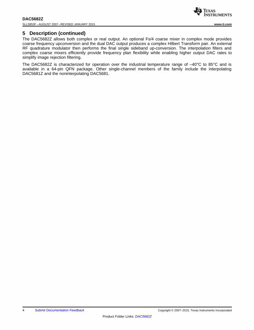
5 Description (continued)The DAC5682Z allows both complex or real output. An optional Fs/4 coarse mixer in complex mode providescoarse frequency upconversion and the dual DAC output produces a complex Hilbert Transform pair. An externalRF quadrature modulator then performs the final single sideband up-conversion. The interpolation filters andcomplex coarse mixers efficiently provide frequency plan flexibility while enabling higher output DAC rates tosimplify image rejection filtering.
The DAC5682Z is characterized for operation over the industrial temperature range of –40°C to 85°C and isavailable in a 64-pin QFN package. Other single-channel members of the family include the interpolatingDAC5681Z and the noninterpolating DAC5681.
4 Submit Documentation Feedback Copyright © 2007–2015, Texas Instruments Incorporated
Product Folder Links: DAC5682Z
45
42
DAC5682Z
GND
CLKINC
D11
P
D11N
D10P
D1
0N
D9
P
D9N
D8P
D8N
DC
LK
P
DC
LK
N
D7P
D7N
D6P
D6N
D5P
D5N
D4P
D4N
D3P
D3N
D2P
D2N
DVDD
D1P
D1N
D0P
D0N
VFUSE
SDO
SDIO
SCLK
SDENBLP
F
DV
DD
AV
DD
AV
DD
IOU
TB
1
IOU
TB
2
EX
TLO
BIA
SJ
EX
TIO
AV
DD
IOU
TA
2
IOU
TA
1
AV
DD
AV
DD
DV
DD
RE
SE
TB
D12N
D12P
D13N
D13P
D14N
D14P
DVDD
D15N
D15P
IOVDD
SYNCN
SYNCP
CLKIN
CLKVDD
49
50
51
52
53
54
55
56
57
58
59
60
61
62
63
64
2
3
4
5
6
7
8
9
10
11
12
13
14
15
1632
31
30
29
28
27
26
25
24
23
22
21
20
19
18
17
47
46
44
43
41
40
39
38
37
36
35
34
33
481
DAC5682Zwww.ti.com SLLS853F –AUGUST 2007–REVISED JANUARY 2015
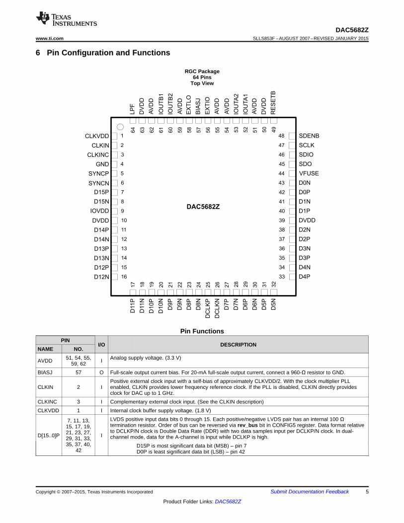
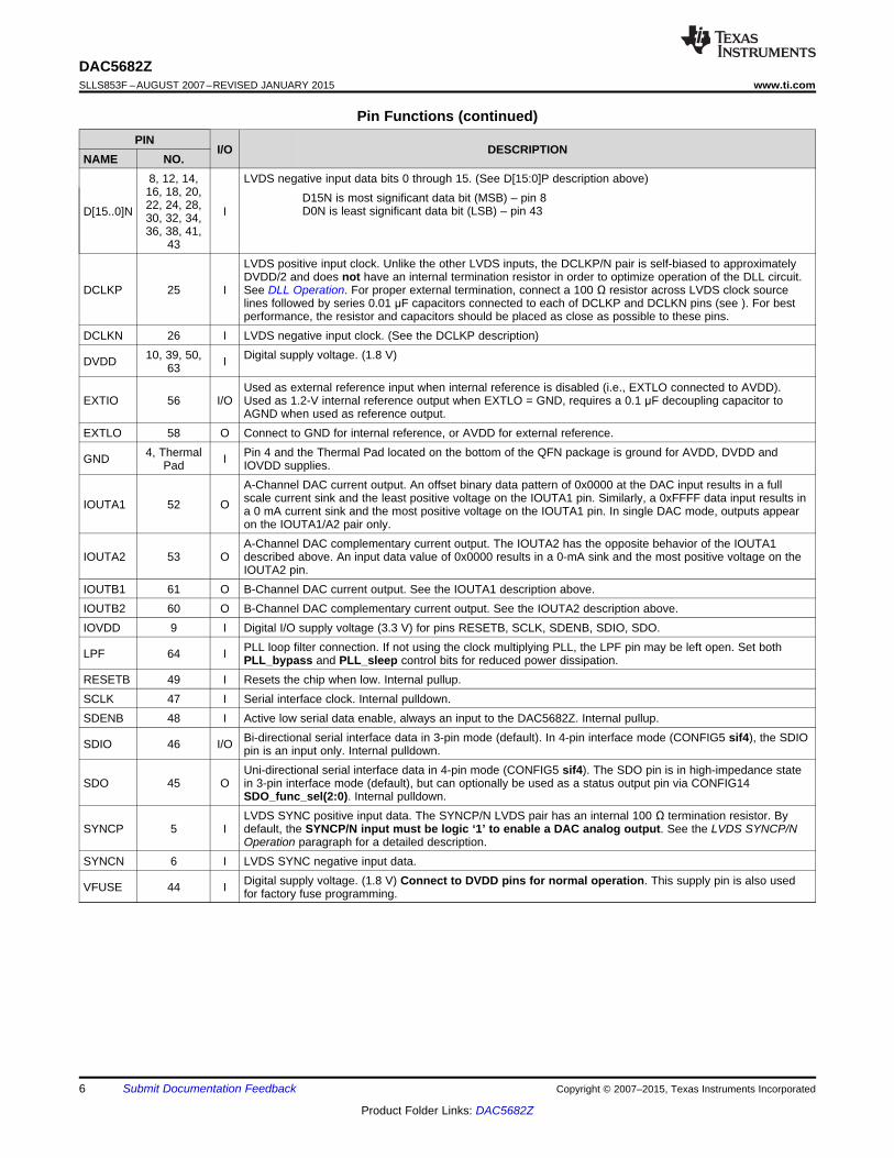
6 Pin Configuration and Functions
RGC Package64 Pins
Top View
Pin FunctionsPIN
I/O DESCRIPTIONNAME NO.
51, 54, 55, Analog supply voltage. (3.3 V)AVDD I59, 62BIASJ 57 O Full-scale output current bias. For 20-mA full-scale output current, connect a 960-Ω resistor to GND.
Positive external clock input with a self-bias of approximately CLKVDD/2. With the clock multiplier PLLCLKIN 2 I enabled, CLKIN provides lower frequency reference clock. If the PLL is disabled, CLKIN directly provides
clock for DAC up to 1 GHz.CLKINC 3 I Complementary external clock input. (See the CLKIN description)CLKVDD 1 I Internal clock buffer supply voltage. (1.8 V)
LVDS positive input data bits 0 through 15. Each positive/negative LVDS pair has an internal 100 Ω7, 11, 13,termination resistor. Order of bus can be reversed via rev_bus bit in CONFIG5 register. Data format relative15, 17, 19,to DCLKP/N clock is Double Data Rate (DDR) with two data samples input per DCLKP/N clock. In dual-21, 23, 27,D[15..0]P I channel mode, data for the A-channel is input while DCLKP is high.29, 31, 33,
35, 37, 40, D15P is most significant data bit (MSB) – pin 742 D0P is least significant data bit (LSB) – pin 42
Copyright © 2007–2015, Texas Instruments Incorporated Submit Documentation Feedback 5
Product Folder Links: DAC5682Z
DAC5682ZSLLS853F –AUGUST 2007–REVISED JANUARY 2015 www.ti.com
Pin Functions (continued)PIN
I/O DESCRIPTIONNAME NO.
8, 12, 14, LVDS negative input data bits 0 through 15. (See D[15:0]P description above)16, 18, 20, D15N is most significant data bit (MSB) – pin 822, 24, 28, D0N is least significant data bit (LSB) – pin 43D[15..0]N I30, 32, 34,36, 38, 41,
43LVDS positive input clock. Unlike the other LVDS inputs, the DCLKP/N pair is self-biased to approximatelyDVDD/2 and does not have an internal termination resistor in order to optimize operation of the DLL circuit.
DCLKP 25 I See DLL Operation. For proper external termination, connect a 100 Ω resistor across LVDS clock sourcelines followed by series 0.01 μF capacitors connected to each of DCLKP and DCLKN pins (see ). For bestperformance, the resistor and capacitors should be placed as close as possible to these pins.
DCLKN 26 I LVDS negative input clock. (See the DCLKP description)10, 39, 50, Digital supply voltage. (1.8 V)DVDD I63
Used as external reference input when internal reference is disabled (i.e., EXTLO connected to AVDD).EXTIO 56 I/O Used as 1.2-V internal reference output when EXTLO = GND, requires a 0.1 μF decoupling capacitor to
AGND when used as reference output.EXTLO 58 O Connect to GND for internal reference, or AVDD for external reference.
4, Thermal Pin 4 and the Thermal Pad located on the bottom of the QFN package is ground for AVDD, DVDD andGND IPad IOVDD supplies.A-Channel DAC current output. An offset binary data pattern of 0x0000 at the DAC input results in a fullscale current sink and the least positive voltage on the IOUTA1 pin. Similarly, a 0xFFFF data input results inIOUTA1 52 O a 0 mA current sink and the most positive voltage on the IOUTA1 pin. In single DAC mode, outputs appearon the IOUTA1/A2 pair only.A-Channel DAC complementary current output. The IOUTA2 has the opposite behavior of the IOUTA1
IOUTA2 53 O described above. An input data value of 0x0000 results in a 0-mA sink and the most positive voltage on theIOUTA2 pin.
IOUTB1 61 O B-Channel DAC current output. See the IOUTA1 description above.IOUTB2 60 O B-Channel DAC complementary current output. See the IOUTA2 description above.IOVDD 9 I Digital I/O supply voltage (3.3 V) for pins RESETB, SCLK, SDENB, SDIO, SDO.
PLL loop filter connection. If not using the clock multiplying PLL, the LPF pin may be left open. Set bothLPF 64 I PLL_bypass and PLL_sleep control bits for reduced power dissipation.RESETB 49 I Resets the chip when low. Internal pullup.SCLK 47 I Serial interface clock. Internal pulldown.SDENB 48 I Active low serial data enable, always an input to the DAC5682Z. Internal pullup.
Bi-directional serial interface data in 3-pin mode (default). In 4-pin interface mode (CONFIG5 sif4), the SDIOSDIO 46 I/O pin is an input only. Internal pulldown.Uni-directional serial interface data in 4-pin mode (CONFIG5 sif4). The SDO pin is in high-impedance state
SDO 45 O in 3-pin interface mode (default), but can optionally be used as a status output pin via CONFIG14SDO_func_sel(2:0). Internal pulldown.LVDS SYNC positive input data. The SYNCP/N LVDS pair has an internal 100 Ω termination resistor. By
SYNCP 5 I default, the SYNCP/N input must be logic ‘1’ to enable a DAC analog output. See the LVDS SYNCP/NOperation paragraph for a detailed description.
SYNCN 6 I LVDS SYNC negative input data.Digital supply voltage. (1.8 V) Connect to DVDD pins for normal operation. This supply pin is also usedVFUSE 44 I for factory fuse programming.
6 Submit Documentation Feedback Copyright © 2007–2015, Texas Instruments Incorporated
Product Folder Links: DAC5682Z
DAC5682Zwww.ti.com SLLS853F –AUGUST 2007–REVISED JANUARY 2015
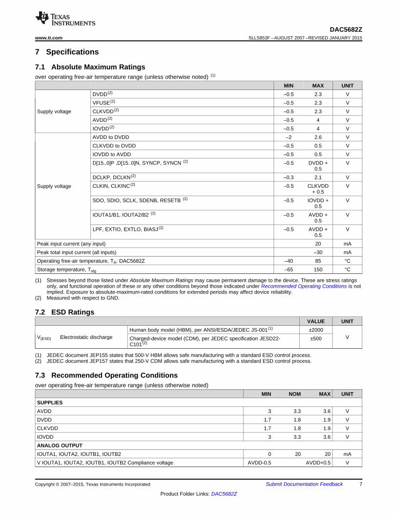
7 Specifications
7.1 Absolute Maximum Ratingsover operating free-air temperature range (unless otherwise noted) (1)
MIN MAX UNITDVDD (2) –0.5 2.3 VVFUSE (2) –0.5 2.3 V
Supply voltage CLKVDD (2) –0.5 2.3 VAVDD (2) –0.5 4 VIOVDD (2) –0.5 4 VAVDD to DVDD –2 2.6 VCLKVDD to DVDD –0.5 0.5 VIOVDD to AVDD –0.5 0.5 VD[15..0]P ,D[15..0]N, SYNCP, SYNCN (2) –0.5 DVDD + V
0.5DCLKP, DCLKN (2) –0.3 2.1 VCLKIN, CLKINC (2) –0.5 CLKVDD VSupply voltage
+ 0.5SDO, SDIO, SCLK, SDENB, RESETB (2) –0.5 IOVDD + V
0.5IOUTA1/B1, IOUTA2/B2 (2) –0.5 AVDD + V
0.5LPF, EXTIO, EXTLO, BIASJ (2) –0.5 AVDD + V
0.5Peak input current (any input) 20 mAPeak total input current (all inputs) –30 mAOperating free-air temperature, TA: DAC5682Z –40 85 °CStorage temperature, Tstg –65 150 °C
(1) Stresses beyond those listed under Absolute Maximum Ratings may cause permanent damage to the device. These are stress ratingsonly, and functional operation of these or any other conditions beyond those indicated under Recommended Operating Conditions is notimplied. Exposure to absolute-maximum-rated conditions for extended periods may affect device reliability.
(2) Measured with respect to GND.
7.2 ESD RatingsVALUE UNIT
Human body model (HBM), per ANSI/ESDA/JEDEC JS-001 (1) ±2000V(ESD) Electrostatic discharge VCharged-device model (CDM), per JEDEC specification JESD22- ±500
C101 (2)
(1) JEDEC document JEP155 states that 500-V HBM allows safe manufacturing with a standard ESD control process.(2) JEDEC document JEP157 states that 250-V CDM allows safe manufacturing with a standard ESD control process.
7.3 Recommended Operating Conditionsover operating free-air temperature range (unless otherwise noted)
MIN NOM MAX UNITSUPPLIESAVDD 3 3.3 3.6 VDVDD 1.7 1.8 1.9 VCLKVDD 1.7 1.8 1.9 VIOVDD 3 3.3 3.6 VANALOG OUTPUTIOUTA1, IOUTA2, IOUTB1, IOUTB2 0 20 20 mAV IOUTA1, IOUTA2, IOUTB1, IOUTB2 Compliance voltage AVDD-0.5 AVDD+0.5 V
Copyright © 2007–2015, Texas Instruments Incorporated Submit Documentation Feedback 7
Product Folder Links: DAC5682Z
DAC5682ZSLLS853F –AUGUST 2007–REVISED JANUARY 2015 www.ti.com
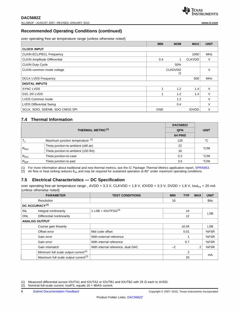
Recommended Operating Conditions (continued)over operating free-air temperature range (unless otherwise noted)
MIN NOM MAX UNITCLOCK INPUTCLKIN ECL/PECL Frequency 1000 MHzCLKIN Amplitude Differential 0.4 1 CLKVDD VCLKIN Duty Cycle 50%CLKIN common mode voltage CLKDVDD V
/2DCLK LVDS Frequency 500 MHzDIGITAL INPUTSSYNC LVDS 1 1.2 1.4 VD15..D0 LVDS 1 1.2 1.4 VLVDS Common mode 1.2 VLVDS Differential Swing 0.4 VSCLK, SDIO, SDENB, SDO CMOS SPI GND IOVDD V
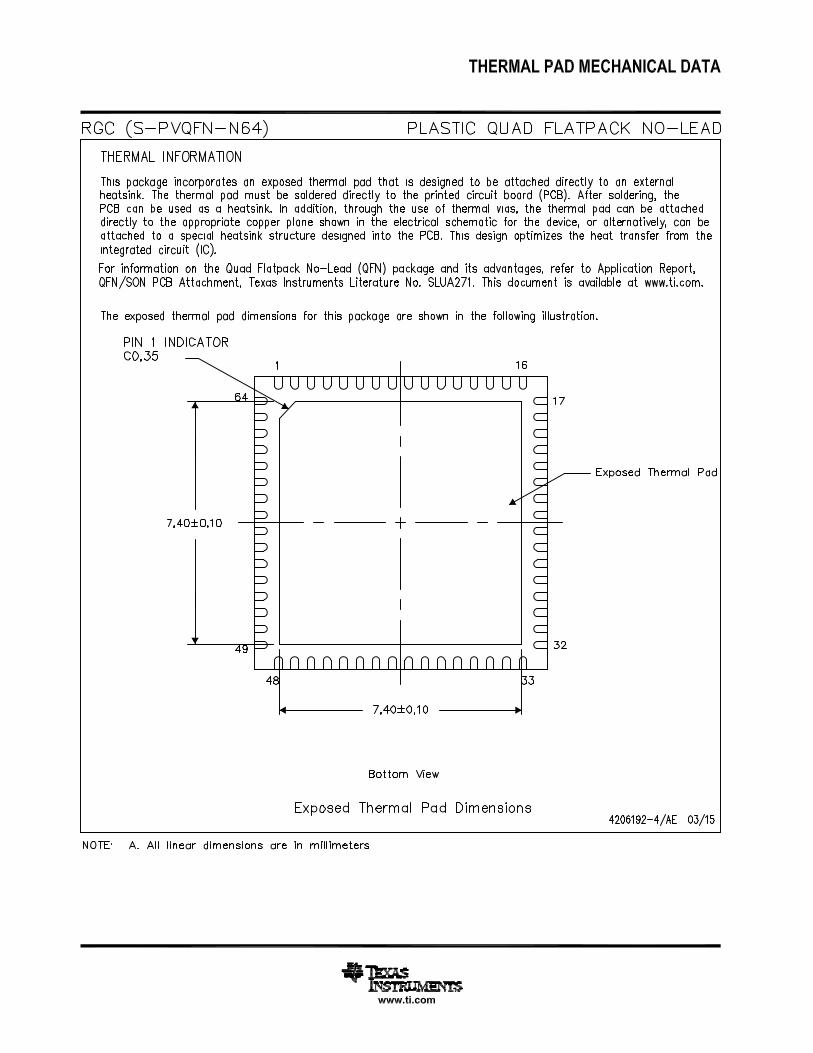
7.4 Thermal InformationDAC5682Z
THERMAL METRIC (1) QFN UNIT64 PINS
TJ Maximum junction temperature (2) 125 °CTheta junction-to-ambient (still air) 22
RθJA °C/WTheta junction-to-ambient (150 lfm) 16
RθJC Theta junction-to-case 0.2 °C/WRθJP Theta junction-to-pad 3.5 °C/W
(1) For more information about traditional and new thermal metrics, see the IC Package Thermal Metrics application report, SPRA953.(2) Air flow or heat sinking reduces θJA and may be required for sustained operation at 85° under maximum operating conditions.
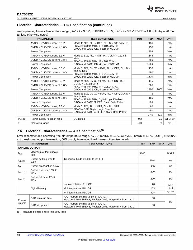
7.5 Electrical Characteristics — DC Specificationover operating free-air temperature range , AVDD = 3.3 V, CLKVDD = 1.8 V, IOVDD = 3.3 V, DVDD = 1.8 V, IoutFS = 20 mA(unless otherwise noted)
PARAMETER TEST CONDITIONS MIN TYP MAX UNITResolution 16 Bits
DC ACCURACY (1)
INL Integral nonlinearity 1 LSB = IOUTFS/216 ±4LSB
DNL Differential nonlinearity ±2ANALOG OUTPUT
Course gain linearity ±0.04 LSBOffset error Mid code offset 0.01 %FSRGain error With external reference 1 %FSRGain error With internal reference 0.7 %FSRGain mismatch With internal reference, dual DAC –2 2 %FSRMinimum full scale output current (2) 2
mAMaximum full scale output current (2) 20
(1) Measured differential across IOUTA1 and IOUTA2 or IOUTB1 and IOUTB2 with 25 Ω each to AVDD.(2) Nominal full-scale current, IoutFS, equals 16 × IBIAS current.
8 Submit Documentation Feedback Copyright © 2007–2015, Texas Instruments Incorporated
Product Folder Links: DAC5682Z
DAC5682Zwww.ti.com SLLS853F –AUGUST 2007–REVISED JANUARY 2015
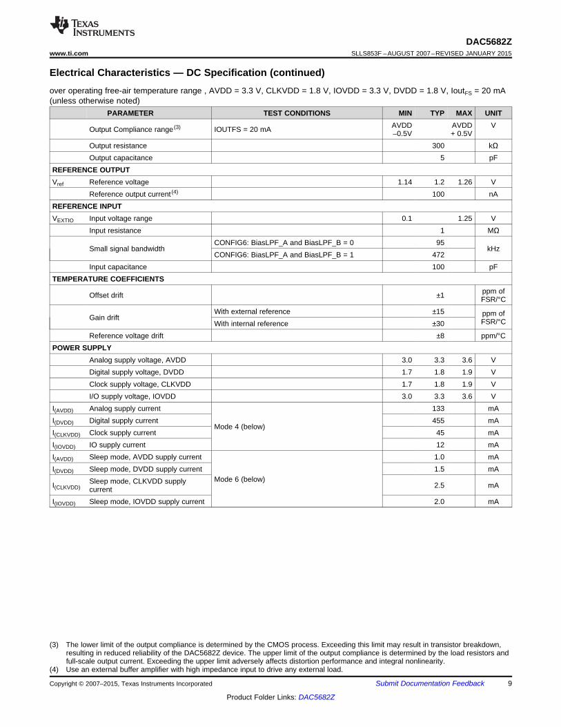
Electrical Characteristics — DC Specification (continued)over operating free-air temperature range , AVDD = 3.3 V, CLKVDD = 1.8 V, IOVDD = 3.3 V, DVDD = 1.8 V, IoutFS = 20 mA(unless otherwise noted)
PARAMETER TEST CONDITIONS MIN TYP MAX UNITAVDD AVDD VOutput Compliance range (3) IOUTFS = 20 mA –0.5V + 0.5V
Output resistance 300 kΩOutput capacitance 5 pF
REFERENCE OUTPUTVref Reference voltage 1.14 1.2 1.26 V
Reference output current (4) 100 nAREFERENCE INPUTVEXTIO Input voltage range 0.1 1.25 V
Input resistance 1 MΩCONFIG6: BiasLPF_A and BiasLPF_B = 0 95
Small signal bandwidth kHzCONFIG6: BiasLPF_A and BiasLPF_B = 1 472
Input capacitance 100 pFTEMPERATURE COEFFICIENTS
ppm ofOffset drift ±1 FSR/°CWith external reference ±15 ppm ofGain drift FSR/°CWith internal reference ±30
Reference voltage drift ±8 ppm/°CPOWER SUPPLY
Analog supply voltage, AVDD 3.0 3.3 3.6 VDigital supply voltage, DVDD 1.7 1.8 1.9 VClock supply voltage, CLKVDD 1.7 1.8 1.9 VI/O supply voltage, IOVDD 3.0 3.3 3.6 V
I(AVDD) Analog supply current 133 mAI(DVDD) Digital supply current 455 mA
Mode 4 (below)I(CLKVDD) Clock supply current 45 mAI(IOVDD) IO supply current 12 mAI(AVDD) Sleep mode, AVDD supply current 1.0 mAI(DVDD) Sleep mode, DVDD supply current 1.5 mA
Mode 6 (below)Sleep mode, CLKVDD supplyI(CLKVDD) 2.5 mAcurrentI(IOVDD) Sleep mode, IOVDD supply current 2.0 mA
(3) The lower limit of the output compliance is determined by the CMOS process. Exceeding this limit may result in transistor breakdown,resulting in reduced reliability of the DAC5682Z device. The upper limit of the output compliance is determined by the load resistors andfull-scale output current. Exceeding the upper limit adversely affects distortion performance and integral nonlinearity.
(4) Use an external buffer amplifier with high impedance input to drive any external load.
Copyright © 2007–2015, Texas Instruments Incorporated Submit Documentation Feedback 9
Product Folder Links: DAC5682Z
DAC5682ZSLLS853F –AUGUST 2007–REVISED JANUARY 2015 www.ti.com
Electrical Characteristics — DC Specification (continued)over operating free-air temperature range , AVDD = 3.3 V, CLKVDD = 1.8 V, IOVDD = 3.3 V, DVDD = 1.8 V, IoutFS = 20 mA(unless otherwise noted)
PARAMETER TEST CONDITIONS MIN TYP MAX UNITAVDD + IOVDD current, 3.3 V Mode 1: 2X2, PLL = OFF, CLKIN = 983.04 MHz 135 mA
FDAC = 983.04 MHz, IF = 184.32 MHzDVDD + CLKVDD current, 1.8 V 450 mADACA and DACB ON, 4 carrier WCDMAPower Dissipation 1255 mWAVDD + IOVDD current, 3.3 V Mode 2: 2X2, PLL = ON (8X), CLKIN = 122.88 145 mA
MHzDVDD + CLKVDD current, 1.8 V 485 mAFDAC = 983.04 MHz, IF = 184.32 MHz1350Power Dissipation mWDACA and DACB ON, 4 carrier WCDMA
AVDD + IOVDD current, 3.3 V Mode 3: 2X4, CMIX0 = Fs/4, PLL = OFF, CLKIN = 135 mA983.04 MHzDVDD + CLKVDD current, 1.8 V 480 mAFDAC = 983.04 MHz, IF = 215.04 MHz
1310Power Dissipation mWDACA and DACB ON, 4 carrier WCDMAP
AVDD + IOVDD current, 3.3 V Mode 4: 2X4, CMIX0 = Fs/4, PLL = ON (8X), 145 mACLKIN = 122.88 MHzDVDD + CLKVDD current, 1.8 V 505 mAFDAC = 983.04 MHz, IF = 215.04 MHz
1400 1600Power Dissipation mWDACA and DACB ON, 4 carrier WCDMAAVDD + IOVDD current, 3.3 V Mode 5: 2X2, CMIX0 = Fs/4, PLL = OFF, CLKIN = 5 mA
983.04 MHzDVDD + CLKVDD current, 1.8 V 185 mAFDAC = 983.04 MHz, Digital Logic Disabled350Power Dissipation mWDACA and DACB SLEEP, Static Data Pattern
AVDD + IOVDD current, 3.3 V Mode 6: 2X4, PLL = OFF, CLKIN = OFF 3.0 mAFDAC = OFF, Digital Logic DisabledDVDD + CLKVDD current, 1.8 V 4.0 mADACA and DACB = SLEEP, Static Data Pattern
Power Dissipation 17.0 30.0 mWPSRR Power supply rejection ratio DC tested –0.2 0.2 %FSR/VT Operating range –40 85 °C
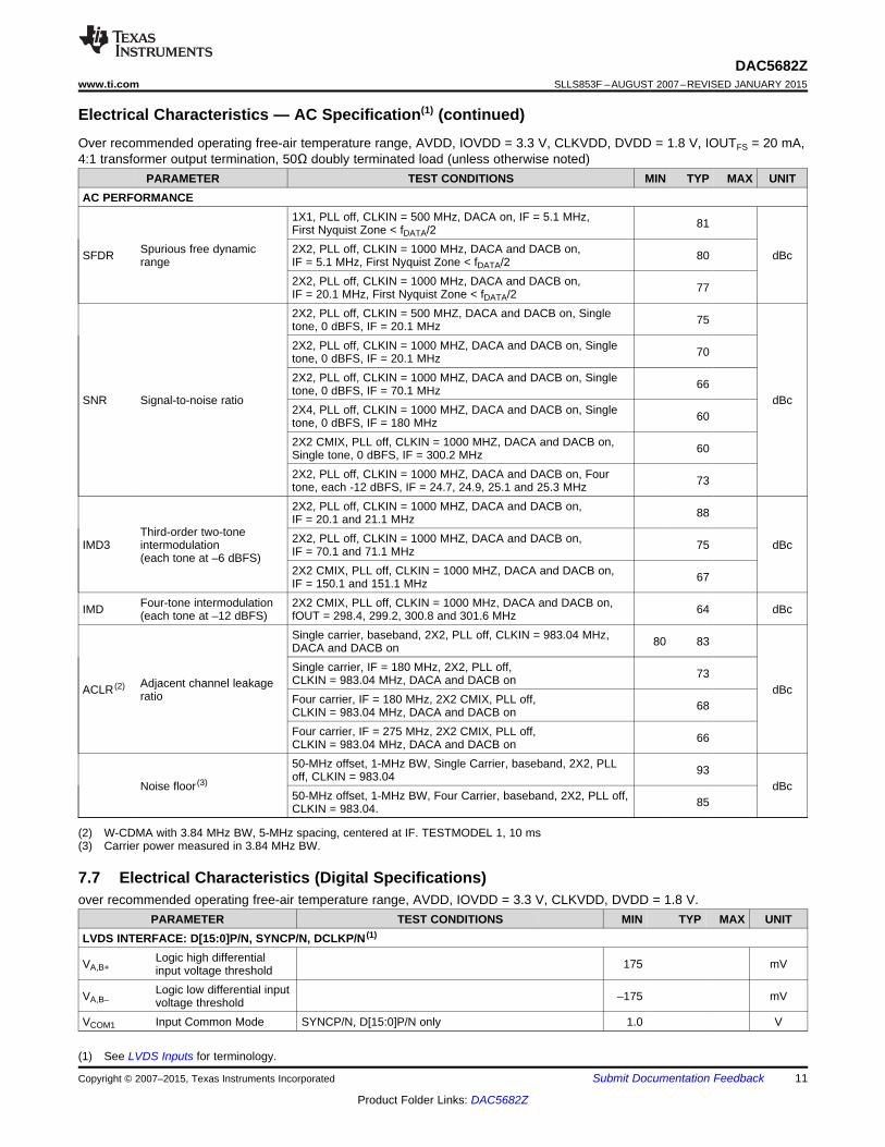
7.6 Electrical Characteristics — AC Specification (1)
Over recommended operating free-air temperature range, AVDD, IOVDD = 3.3 V, CLKVDD, DVDD = 1.8 V, IOUTFS = 20 mA,4:1 transformer output termination, 50Ω doubly terminated load (unless otherwise noted)
PARAMETER TEST CONDITIONS MIN TYP MAX UNITANALOG OUTPUT
Maximum output updatefCLK 1000 MSPSrateOutput settling time to Transition: Code 0x0000 to 0xFFFFts(DAC) 10.4 ns0.1%
tpd Output propagation delay 2.5 nsOutput rise time 10% totr(IOUT) 220 ps90%Output fall time 90% totf(IOUT) 220 ps10%
No interpolation, PLL Off 78 DACDigital latency x2 interpolation, PLL Off 163 clock
cyclesx4 interpolation, PLL Off 308IOUT current settling to 1% of IOUTFS.DAC wake-up time 80Measured from SDENB; Register 0x06, toggle Bit 4 from 1 to 0.Power- μsup time IOUT current settling to 1% of IOUTFS.DAC sleep time 80Measured from SDENB; Register 0x06, toggle Bit 4 from 0 to 1.
(1) Measured single-ended into 50 Ω load.
10 Submit Documentation Feedback Copyright © 2007–2015, Texas Instruments Incorporated
Product Folder Links: DAC5682Z
DAC5682Zwww.ti.com SLLS853F –AUGUST 2007–REVISED JANUARY 2015
Electrical Characteristics — AC Specification(1) (continued)Over recommended operating free-air temperature range, AVDD, IOVDD = 3.3 V, CLKVDD, DVDD = 1.8 V, IOUTFS = 20 mA,4:1 transformer output termination, 50Ω doubly terminated load (unless otherwise noted)
PARAMETER TEST CONDITIONS MIN TYP MAX UNITAC PERFORMANCE
1X1, PLL off, CLKIN = 500 MHz, DACA on, IF = 5.1 MHz, 81First Nyquist Zone < fDATA/2Spurious free dynamic 2X2, PLL off, CLKIN = 1000 MHz, DACA and DACB on,SFDR 80 dBcrange IF = 5.1 MHz, First Nyquist Zone < fDATA/2
2X2, PLL off, CLKIN = 1000 MHz, DACA and DACB on, 77IF = 20.1 MHz, First Nyquist Zone < fDATA/22X2, PLL off, CLKIN = 500 MHZ, DACA and DACB on, Single 75tone, 0 dBFS, IF = 20.1 MHz2X2, PLL off, CLKIN = 1000 MHZ, DACA and DACB on, Single 70tone, 0 dBFS, IF = 20.1 MHz2X2, PLL off, CLKIN = 1000 MHZ, DACA and DACB on, Single 66tone, 0 dBFS, IF = 70.1 MHz
SNR Signal-to-noise ratio dBc2X4, PLL off, CLKIN = 1000 MHZ, DACA and DACB on, Single 60tone, 0 dBFS, IF = 180 MHz2X2 CMIX, PLL off, CLKIN = 1000 MHZ, DACA and DACB on, 60Single tone, 0 dBFS, IF = 300.2 MHz2X2, PLL off, CLKIN = 1000 MHZ, DACA and DACB on, Four 73tone, each -12 dBFS, IF = 24.7, 24.9, 25.1 and 25.3 MHz2X2, PLL off, CLKIN = 1000 MHZ, DACA and DACB on, 88IF = 20.1 and 21.1 MHz
Third-order two-tone 2X2, PLL off, CLKIN = 1000 MHZ, DACA and DACB on,IMD3 intermodulation 75 dBcIF = 70.1 and 71.1 MHz(each tone at –6 dBFS)2X2 CMIX, PLL off, CLKIN = 1000 MHZ, DACA and DACB on, 67IF = 150.1 and 151.1 MHz
Four-tone intermodulation 2X2 CMIX, PLL off, CLKIN = 1000 MHz, DACA and DACB on,IMD 64 dBc(each tone at –12 dBFS) fOUT = 298.4, 299.2, 300.8 and 301.6 MHzSingle carrier, baseband, 2X2, PLL off, CLKIN = 983.04 MHz, 80 83DACA and DACB onSingle carrier, IF = 180 MHz, 2X2, PLL off, 73CLKIN = 983.04 MHz, DACA and DACB onAdjacent channel leakageACLR (2) dBcratio Four carrier, IF = 180 MHz, 2X2 CMIX, PLL off, 68CLKIN = 983.04 MHz, DACA and DACB onFour carrier, IF = 275 MHz, 2X2 CMIX, PLL off, 66CLKIN = 983.04 MHz, DACA and DACB on50-MHz offset, 1-MHz BW, Single Carrier, baseband, 2X2, PLL 93off, CLKIN = 983.04
Noise floor (3) dBc50-MHz offset, 1-MHz BW, Four Carrier, baseband, 2X2, PLL off, 85CLKIN = 983.04.
(2) W-CDMA with 3.84 MHz BW, 5-MHz spacing, centered at IF. TESTMODEL 1, 10 ms(3) Carrier power measured in 3.84 MHz BW.
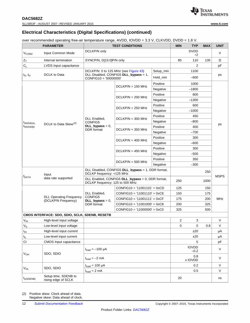
7.7 Electrical Characteristics (Digital Specifications)over recommended operating free-air temperature range, AVDD, IOVDD = 3.3 V, CLKVDD, DVDD = 1.8 V.
PARAMETER TEST CONDITIONS MIN TYP MAX UNITLVDS INTERFACE: D[15:0]P/N, SYNCP/N, DCLKP/N (1)
Logic high differentialVA,B+ 175 mVinput voltage thresholdLogic low differential inputVA,B– –175 mVvoltage threshold
VCOM1 Input Common Mode SYNCP/N, D[15:0]P/N only 1.0 V
(1) See LVDS Inputs for terminology.
Copyright © 2007–2015, Texas Instruments Incorporated Submit Documentation Feedback 11
Product Folder Links: DAC5682Z
DAC5682ZSLLS853F –AUGUST 2007–REVISED JANUARY 2015 www.ti.com
Electrical Characteristics (Digital Specifications) (continued)over recommended operating free-air temperature range, AVDD, IOVDD = 3.3 V, CLKVDD, DVDD = 1.8 V.
PARAMETER TEST CONDITIONS MIN TYP MAX UNITDCLKP/N only DVDDVCOM2 Input Common Mode V÷2
ZT Internal termination SYNCP/N, D[15:0]P/N only 85 110 135 ΩCL LVDS Input capacitance 2 pF
DCLKP/N: 0 to 125 MHz (see Figure 43) Setup_min 1100tS, tH DCLK to Data DLL Disabled, CONFIG5 DLL_bypass = 1, ps
Hold_min –600CONFIG10 = '00000000'Positive 1000
DCLKP/N = 150 MHzNegative –1800Positive 800
DCLKP/N = 200 MHzNegative –1300Positive 600
DCLKP/N = 250 MHzNegative –1000Positive 450
DLL Enabled, DCLKP/N = 300 MHzNegative –800tSKEW(A), CONFIG5DCLK to Data Skew (2) pstSKEW(B) DLL_bypass = 0, Positive 400
DCLKP/N = 350 MHzDDR formatNegative –700Positive 300
DCLKP/N = 400 MHzNegative –600Positive 300
DCLKP/N = 450 MHzNegative –500Positive 350
DCLKP/N = 500 MHzNegative –300
DLL Disabled, CONFIG5 DLL_bypass = 1, DDR format, 250DCLKP frequency: <125 MHzInputfDATA MSPSdata rate supported DLL Enabled, CONFIG5 DLL_bypass = 0, DDR format, 250 1000DCLKP frequency: 125 to 500 MHzCONFIG10 = '11001101' = 0xCD 125 150
DLL Enabled, CONFIG10 = '11001110' = 0xCE 150 175DLL Operating Frequency CONFIG5 CONFIG10 = '11001111' = 0xCF 175 200 MHz(DCLKP/N Frequency) DLL_bypass = 0,
CONFIG10 = '11001000' = 0xC8 200 325DDR formatCONFIG10 = '11000000' = 0xC0 325 500
CMOS INTERFACE: SDO, SDIO, SCLK, SDENB, RESETBVIH High-level input voltage 2 3 VVIL Low-level input voltage 0 0 0.8 VIIH High-level input current ±20 μAIIL Low-level input current ±20 μACI CMOS Input capacitance 5 pF
IOVDDIload = –100 μA V–0.2VOH SDO, SDIO
0.8Iload = –2 mA Vx IOVDDIload = 100 μA 0.2 V
VOL SDO, SDIOIload = 2 mA 0.5 V
Setup time, SDENB tots(SDENB) 20 nsrising edge of SCLK
(2) Positive skew: Clock ahead of data.Negative skew: Data ahead of clock.
12 Submit Documentation Feedback Copyright © 2007–2015, Texas Instruments Incorporated
Product Folder Links: DAC5682Z
DAC5682Zwww.ti.com SLLS853F –AUGUST 2007–REVISED JANUARY 2015
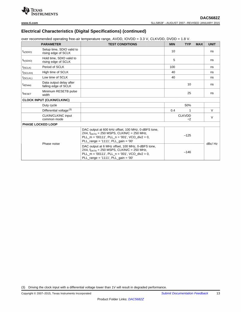
Electrical Characteristics (Digital Specifications) (continued)over recommended operating free-air temperature range, AVDD, IOVDD = 3.3 V, CLKVDD, DVDD = 1.8 V.
PARAMETER TEST CONDITIONS MIN TYP MAX UNITSetup time, SDIO valid tots(SDIO) 10 nsrising edge of SCLKHold time, SDIO valid toth(SDIO) 5 nsrising edge of SCLK
t(SCLK) Period of SCLK 100 nst(SCLKH) High time of SCLK 40 nst(SCLKL) Low time of SCLK 40 ns
Data output delay aftertd(Data) 10 nsfalling edge of SCLKMinimum RESETB pulsetRESET 25 nswidth
CLOCK INPUT (CLKIN/CLKINC)Duty cycle 50%Differential voltage (3) 0.4 1 VCLKIN/CLKINC input CLKVDD Vcommon mode ÷2
PHASE LOCKED LOOPDAC output at 600 kHz offset, 100 MHz, 0-dBFS tone,2X4, fDATA = 250 MSPS, CLKIN/C = 250 MHz,
–125PLL_m = '00111', PLL_n = '001', VCO_div2 = 0,PLL_range = '1111', PLL_gain = '00'
Phase noise dBc/ HzDAC output at 6 MHz offset, 100 MHz, 0-dBFS tone,2X4, fDATA = 250 MSPS, CLKIN/C = 250 MHz,
–146PLL_m = '00111', PLL_n = '001', VCO_div2 = 0,PLL_range = '1111', PLL_gain = '00'
(3) Driving the clock input with a differential voltage lower than 1V will result in degraded performance.
Copyright © 2007–2015, Texas Instruments Incorporated Submit Documentation Feedback 13
Product Folder Links: DAC5682Z
DAC5682ZSLLS853F –AUGUST 2007–REVISED JANUARY 2015 www.ti.com
Electrical Characteristics (Digital Specifications) (continued)over recommended operating free-air temperature range, AVDD, IOVDD = 3.3 V, CLKVDD, DVDD = 1.8 V.
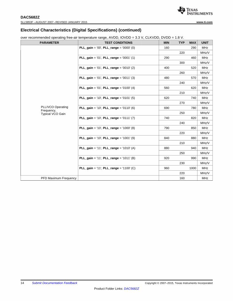
PARAMETER TEST CONDITIONS MIN TYP MAX UNITPLL_gain = '00', PLL_range = '0000' (0) 160 290 MHz
220 MHz/VPLL_gain = '01', PLL_range = '0001' (1) 290 460 MHz
300 MHz/VPLL_gain = '01', PLL_range = '0010' (2) 400 520 MHz
260 MHz/VPLL_gain = '01', PLL_range = '0011' (3) 480 570 MHz
240 MHz/VPLL_gain = '01', PLL_range = '0100' (4) 560 620 MHz
210 MHz/VPLL_gain = '10', PLL_range = '0101' (5) 620 740 MHz
270 MHz/VPLL/VCO Operating PLL_gain = '10', PLL_range = '0110' (6) 690 780 MHzFrequency,
250 MHz/VTypical VCO GainPLL_gain = '10', PLL_range = '0111' (7) 740 820 MHz
240 MHz/VPLL_gain = '10', PLL_range = '1000' (8) 790 850 MHz
220 MHz/VPLL_gain = '10', PLL_range = '1001' (9) 840 880 MHz
210 MHz/VPLL_gain = '11', PLL_range = '1010' (A) 880 940 MHz
250 MHz/VPLL_gain = '11', PLL_range = '1011' (B) 920 990 MHz
230 MHz/VPLL_gain = '11', PLL_range = '1100' (C) 960 1000 MHz
220 MHz/VPFD Maximum Frequency 160 MHz
14 Submit Documentation Feedback Copyright © 2007–2015, Texas Instruments Incorporated
Product Folder Links: DAC5682Z
60
65
70
75
80
85
90
95
0 10 20 30 40 50
F = 250 MSPS,
x4 Interpolation,PLL Off
data
0 dBFS
-6 dBFS-12 dBFS
IF - Intermediate Frequency - MHz
SF
DR
- S
pu
rio
us
Fre
e D
yn
am
ic R
an
ge
- d
Bc
f - Frequency - MHz
0 50 100 150 200 250 300 350 400 450 500
-80
-70
-60
-50
-40
-30
-20
-10
0
10
Po
wer
- d
Bm
F = 250 MSPS,
F = -80 MHz Complex,
(-80+250=170)IF = 170 MHz, CMIX, F /4
x4 InterpolationPLL Off
data
IN
S
-90
-80
-70
-60
-50
-40
-30
-20
-10
0
10
Po
wer
- d
Bm
f - Frequency - MHz
0 50 100 150 200 250 300 350 400 450 500
F = 250 MSPS,
F = 20 MHz Complex,
IF = 20 MHz,x4 InterpolationPLL Off
data
IN
f - Frequency - MHz
-90
-80
-70
-60
-50
-40
-30
-20
-10
0
10
Po
wer
- d
Bm
0 50 100 150 200 250 300 350 400 450 500
F = 250 MSPS,
F = 20 MHz Complex,
IF = 270 MHz,x4 InterpolationCMIX F /4
PLL Off
data
IN
S
DAC5682Zwww.ti.com SLLS853F –AUGUST 2007–REVISED JANUARY 2015
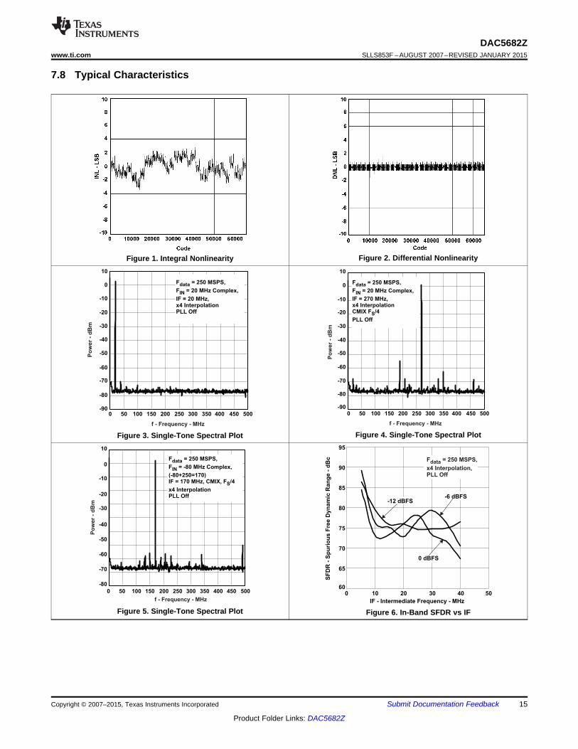
7.8 Typical Characteristics
Figure 2. Differential NonlinearityFigure 1. Integral Nonlinearity
Figure 4. Single-Tone Spectral PlotFigure 3. Single-Tone Spectral Plot
Figure 5. Single-Tone Spectral Plot Figure 6. In-Band SFDR vs IF
Copyright © 2007–2015, Texas Instruments Incorporated Submit Documentation Feedback 15
Product Folder Links: DAC5682Z
65
70
75
80
85
0 61.44 122.88 184.32 245.76
AC
LR
- d
Bc
f - Frequency - MHz
Fdata = 491.52 MSPS,F = IFIN
PLL Off
PLL On
-90
-80
-70
-60
-50
-40
-30
-20
-10
0
10
248.5 249.0 249.5 250.0 251.0 252.0250.5 251.5 252.5
f - Frequency - MHz
Po
wer
- d
Bm
Fdata = 500 MSPS,
F = 0 0.5 MHz,
IF = 250 MHz (Fs/4)x2 InterpolationPLL Off
IN ±
f - Frequency - MHz
-100
-90
-80
-70
-60
-50
-40
-30
-20
-10
0
Po
wer
- d
Bm
35 36 37 38 39 40 41 42 43 44 45
F = 500 MSPS,
F = 40 0.5 MHz Real,
IF = 40 MHz,x2 InterpolationPLL Off
data
IN ±
45
50
55
60
65
70
75
80
85
-30 -25 -20 -15 -10 -5 0
89.5 and 90.5 MHz(CMIX Off)
Amplitude - dBFS
IMD
- d
Bc
Shift to 215 MHz(F /4 On)S
Shift to 340 MHz(F /8 On)S
F = 250 MSPS
F = 90 MHz ±0.5 MHz Complex
x4 Interpolation, PLL OffThree modes: CMIX, F /8, and F /4
data
in
S S
50
55
60
65
70
75
80
85
90
0 40 80 120 160 200 240 280 320
IMD
- d
Bc
IF - Intermediate Frequency - MHz
F = 250 MSPS,
x4 Interpolation,PLL Off
data
40
65
70
75
80
85
90
0 50 100 150 200 250 300 450 500
SF
DR
- S
pu
rio
us
-Fre
e D
yn
am
ic R
an
ge -
dB
c
IF - Intermediate Frequency - MHz
350 400
60
55
50
45
F = 250 MSPS,
x4 Interpolation,PLL Off
data
DAC5682ZSLLS853F –AUGUST 2007–REVISED JANUARY 2015 www.ti.com
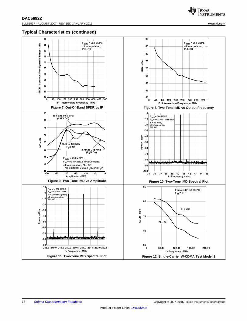
Typical Characteristics (continued)
Figure 7. Out-Of-Band SFDR vs IF Figure 8. Two-Tone IMD vs Output Frequency
Figure 9. Two-Tone IMD vs Amplitude Figure 10. Two-Tone IMD Spectral Plot
Figure 11. Two-Tone IMD Spectral Plot Figure 12. Single-Carrier W-CDMA Test Model 1
16 Submit Documentation Feedback Copyright © 2007–2015, Texas Instruments Incorporated
Product Folder Links: DAC5682Z
-120
-110
-100
-90
-80
-70
-60
-50
-40
-30
-20
233 238 243 248 253 258
f - Frequency - MHz
Po
wer
- d
Bm
Carrier Power: -8.99 dBm,ACLR (5 MHz): 68.22 dB,ACLR (10 MHz): 74.15 dB,F = 245.76 MSPS,
IF = Baseband,x4 InterpolationCMIX PLL Off
data
-120
-110
-100
-90
-80
-70
-60
-50
-40
-30
-20
233 238 243 248 253 258
f - Frequency - MHz
Po
wer
- d
Bm
Carrier Power: -8.99 dBm,ACLR (5 MHz): 64.23 dB,ACLR (10 MHz): 71.27 dB,F = 245.76 MSPS,
IF = Baseband,x4 InterpolationCMIX PLL On
data
-120
-110
-100
-90
-80
-70
-60
-50
-40
-30
-20
172 177 182 187 192 197
f - Frequency - MHz
Po
wer
- d
Bm
Carrier Power: -8.66 dBm,ACLR (5 MHz): 68.61 dB,ACLR (10 MHz): 75.91 dB,F = 491.52 MSPS,
IF = 184.32 MHz,x2 InterpolationPLL On
data
-120
-110
-100
-90
-80
-70
-60
-50
-40
-30
-20
172 177 182 187 192 197f - Frequency - MHz
Po
wer
- d
Bm
Carrier Power: -8.66 dBm,ACLR (5 MHz): 73.19 dB,ACLR (10 MHz): 80.07 dB,F = 491.52 MSPS,
IF = 184.32 MHz,x2 InterpolationPLL Off
data
-120
-110
-100
-90
-80
-70
-60
-50
-40
-30
-20
48.9 53.9 58.9 63.9 68.9 73.9
f - Frequency - MHz
Po
wer
- d
Bm
Carrier Power: -7.60 dBm,ACLR (5 MHz): 77.49 dB,ACLR (10 MHz): 82.45 dB,F = 245.76 MSPS,
IF = 61.44 MHz,x4 InterpolationPLL On
data
-120
-110
-100
-90
-80
-70
-60
-50
-40
-30
-20
48.9 53.9 58.9 63.9 68.9 73.9f - Frequency - MHz
Po
wer
- d
Bm
Carrier Power: -7.60 dBm,ACLR (5 MHz): 80.66 dB,ACLR (10 MHz): 82.61 dB,F = 245.76 MSPS,
IF = 61.44 MHz,x4 InterpolationPLL Off
data
DAC5682Zwww.ti.com SLLS853F –AUGUST 2007–REVISED JANUARY 2015
Typical Characteristics (continued)
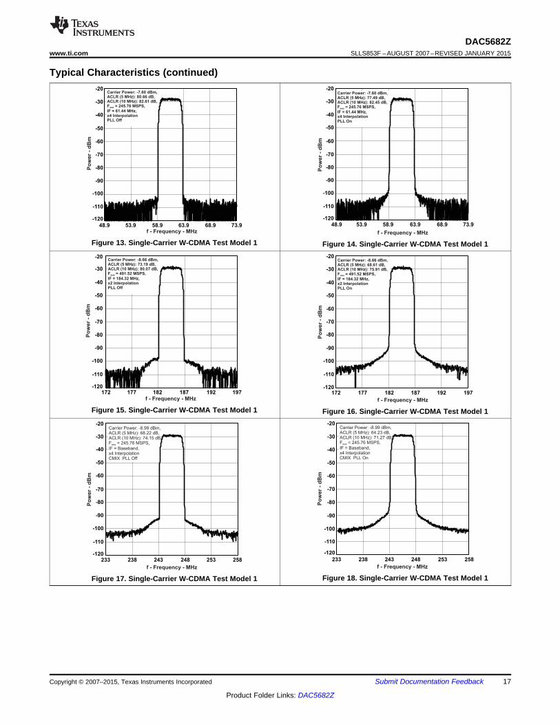
Figure 13. Single-Carrier W-CDMA Test Model 1 Figure 14. Single-Carrier W-CDMA Test Model 1
Figure 15. Single-Carrier W-CDMA Test Model 1 Figure 16. Single-Carrier W-CDMA Test Model 1
Figure 18. Single-Carrier W-CDMA Test Model 1Figure 17. Single-Carrier W-CDMA Test Model 1
Copyright © 2007–2015, Texas Instruments Incorporated Submit Documentation Feedback 17
Product Folder Links: DAC5682Z
-120
-110
-100
-90
-80
-70
-60
-50
-40
-30
-20
160 165 170 175 180 185 190 195 200 205 210
f - Frequency - MHz
Po
wer
- d
Bm
Carrier Power: -15.20 dBm,ACLR (5 MHz): 66.53 dB,ACLR (10 MHz): 69.68 dB,F = 491.52 MSPS,
IF = 184.32 MHz,x2 InterpolationPLL On
data
-120
-110
-100
-90
-80
-70
-60
-50
-40
-30
-20
160 165 170 175 180 185 190 195 200 205 210
f - Frequency - MHz
Po
wer
- d
Bm
Carrier Power: -15.85 dBm,ACLR (5 MHz): 65.85 dB,ACLR (10 MHz): 69.60 dB,F = 491.52 MSPS,
IF = 184.32 MHz,x2 InterpolationPLL On
data
-120
-110
-100
-90
-80
-70
-60
-50
-40
-30
-20
160 165 170 175 180 185 190 195 200 205 210
f - Frequency - MHz
Po
wer
- d
Bm
Carrier Power: -15.20 dBm,ACLR (5 MHz): 71.18 dB,ACLR (10 MHz): 72.26 dB,F = 491.52 MSPS,
IF = 184.32 MHz,x2 InterpolationPLL Off
data
-120
-110
-100
-90
-80
-70
-60
-50
-40
-30
-20
160 165 170 175 180 185 190 195 200 205 210
f - Frequency - MHz
Po
wer
- d
Bm
Carrier Power: -11.98 dBm,ACLR (5 MHz): 66.16 dB,ACLR (10 MHz): 72.84 dB,F = 491.52 MSPS,
IF = 184.32 MHz,x2 InterpolationPLL On
data
-120
-110
-100
-90
-80
-70
-60
-50
-40
-30
-20
160 165 170 175 180 185 190 195 200 205 210
f - Frequency - MHz
Po
wer
- d
Bm
Carrier Power: -11.98 dBm,ACLR (5 MHz): 69.74 dB,ACLR (10 MHz): 75.41 dB,F = 491.52 MSPS,
IF = 184.32 MHz,x2 InterpolationPLL Off
data
DAC5682ZSLLS853F –AUGUST 2007–REVISED JANUARY 2015 www.ti.com
Typical Characteristics (continued)
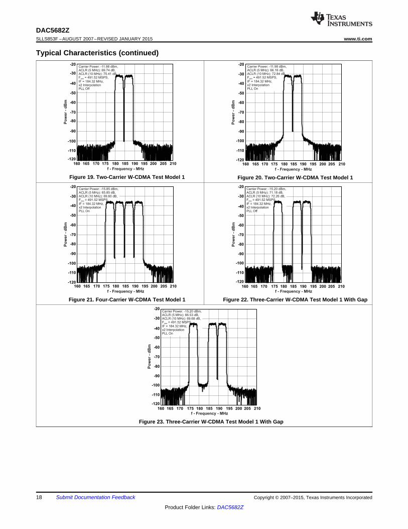
Figure 19. Two-Carrier W-CDMA Test Model 1 Figure 20. Two-Carrier W-CDMA Test Model 1
Figure 21. Four-Carrier W-CDMA Test Model 1 Figure 22. Three-Carrier W-CDMA Test Model 1 With Gap
Figure 23. Three-Carrier W-CDMA Test Model 1 With Gap
18 Submit Documentation Feedback Copyright © 2007–2015, Texas Instruments Incorporated
Product Folder Links: DAC5682Z
CLKIN
CLKINC
LP
F
DCLKP
CL
KV
DD
(1.8
V)
DV
DD
(1.8
V)
VF
US
E(1
.8V
)
GN
D
1.2V
Reference
EXTIO
EXTLO
BIASJ
IOUTB1
IOUTB2
16bit
DAC
Clock MultiplyingPLL 2x-32x
D0P
D0N
D15P
D15N
DCLKN
SD
IO
IOV
DD
(3.3
V)
SYNCP
SYNCN
SD
EN
B
RE
SE
TB
SC
LK
SD
O
10
01
00
IOUTA1
IOUTA2
16bit
DAC
Delay LockLoop (DLL)
FIR
1E
na
ble
FIR
0 E
na
ble
FIFO Sync Disable
Sync & Control
x2 x2
x216
DLL Control
x2
FIR0
CM
1M
od
e
Mode ControlDACA_gain
DACB_gain
4
4D
ela
yV
alu
eSYNC=’0->1'(transition)
10
0
16
PLL Control
ClockDistribution
FDAC
FDAC/2
PLL Bypass
2
AV
DD
(3.3
V)
PLL Enable
16
BA
CM
IX0
[Mo
de
s=
LP
,H
P,
Fs/8
,-F
s/8
]
DA
CD
ela
y(0
-3)
B-O
ffse
t
13
A-Offset
13
FIR1
(x2 Bypass) (x1 Bypass)
CM
0M
od
e
8S
am
ple
FIF
O
DD
RD
e-i
nte
rle
ave
TXEnable=’1'
FDAC/4
SW_Sync
22
47t 76dB HBF 47t 76dB HBF
47t 76dB HBF47t 76dB HBF
CM
IX1
[Mo
de
s=
LP
,H
P,
Fs/4
,-F
s/4
]
16
Sync Disable
DAC5682Zwww.ti.com SLLS853F –AUGUST 2007–REVISED JANUARY 2015
8 Detailed Description
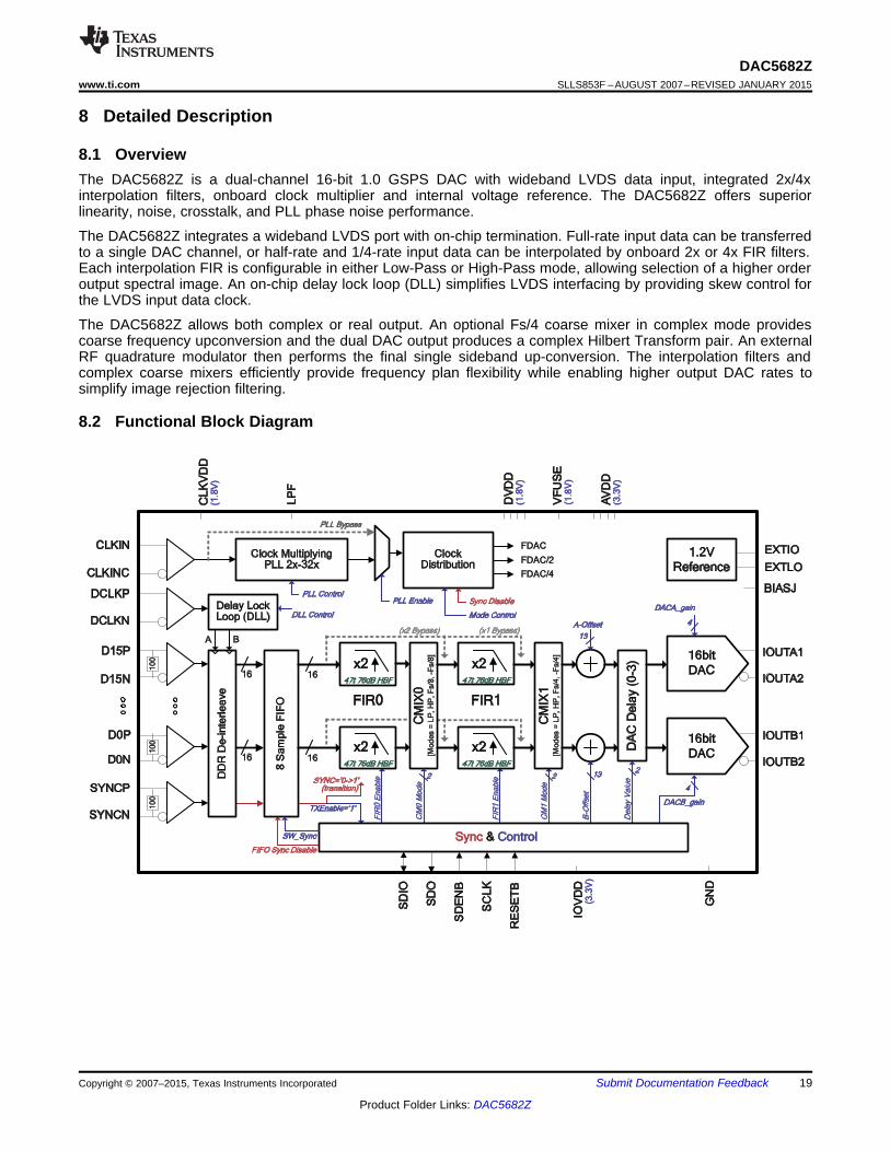
8.1 OverviewThe DAC5682Z is a dual-channel 16-bit 1.0 GSPS DAC with wideband LVDS data input, integrated 2x/4xinterpolation filters, onboard clock multiplier and internal voltage reference. The DAC5682Z offers superiorlinearity, noise, crosstalk, and PLL phase noise performance.
The DAC5682Z integrates a wideband LVDS port with on-chip termination. Full-rate input data can be transferredto a single DAC channel, or half-rate and 1/4-rate input data can be interpolated by onboard 2x or 4x FIR filters.Each interpolation FIR is configurable in either Low-Pass or High-Pass mode, allowing selection of a higher orderoutput spectral image. An on-chip delay lock loop (DLL) simplifies LVDS interfacing by providing skew control forthe LVDS input data clock.
The DAC5682Z allows both complex or real output. An optional Fs/4 coarse mixer in complex mode providescoarse frequency upconversion and the dual DAC output produces a complex Hilbert Transform pair. An externalRF quadrature modulator then performs the final single sideband up-conversion. The interpolation filters andcomplex coarse mixers efficiently provide frequency plan flexibility while enabling higher output DAC rates tosimplify image rejection filtering.
8.2 Functional Block Diagram
Copyright © 2007–2015, Texas Instruments Incorporated Submit Documentation Feedback 19
Product Folder Links: DAC5682Z
DAC5682ZSLLS853F –AUGUST 2007–REVISED JANUARY 2015 www.ti.com
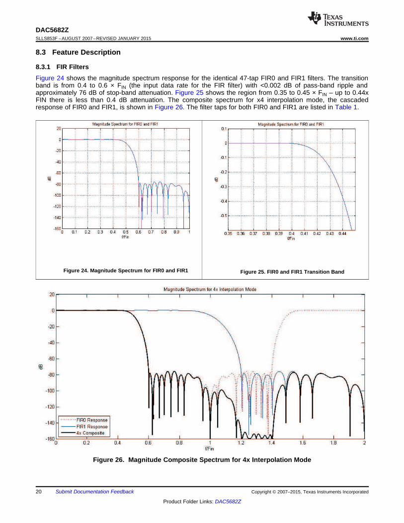
8.3 Feature Description
8.3.1 FIR FiltersFigure 24 shows the magnitude spectrum response for the identical 47-tap FIR0 and FIR1 filters. The transitionband is from 0.4 to 0.6 × FIN (the input data rate for the FIR filter) with <0.002 dB of pass-band ripple andapproximately 76 dB of stop-band attenuation. Figure 25 shows the region from 0.35 to 0.45 × FIN – up to 0.44xFIN there is less than 0.4 dB attenuation. The composite spectrum for x4 interpolation mode, the cascadedresponse of FIR0 and FIR1, is shown in Figure 26. The filter taps for both FIR0 and FIR1 are listed in Table 1.
Figure 24. Magnitude Spectrum for FIR0 and FIR1 Figure 25. FIR0 and FIR1 Transition Band
Figure 26. Magnitude Composite Spectrum for 4x Interpolation Mode
20 Submit Documentation Feedback Copyright © 2007–2015, Texas Instruments Incorporated
Product Folder Links: DAC5682Z
DAC5682Zwww.ti.com SLLS853F –AUGUST 2007–REVISED JANUARY 2015
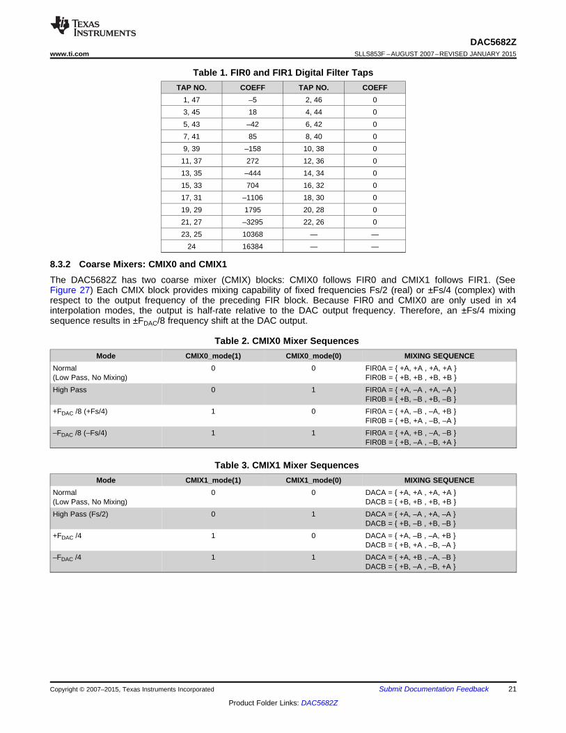
Table 1. FIR0 and FIR1 Digital Filter TapsTAP NO. COEFF TAP NO. COEFF
1, 47 –5 2, 46 03, 45 18 4, 44 05, 43 –42 6, 42 07, 41 85 8, 40 09, 39 –158 10, 38 0
11, 37 272 12, 36 013, 35 –444 14, 34 015, 33 704 16, 32 017, 31 –1106 18, 30 019, 29 1795 20, 28 021, 27 –3295 22, 26 023, 25 10368 — —
24 16384 — —
8.3.2 Coarse Mixers: CMIX0 and CMIX1The DAC5682Z has two coarse mixer (CMIX) blocks: CMIX0 follows FIR0 and CMIX1 follows FIR1. (SeeFigure 27) Each CMIX block provides mixing capability of fixed frequencies Fs/2 (real) or ±Fs/4 (complex) withrespect to the output frequency of the preceding FIR block. Because FIR0 and CMIX0 are only used in x4interpolation modes, the output is half-rate relative to the DAC output frequency. Therefore, an ±Fs/4 mixingsequence results in ±FDAC/8 frequency shift at the DAC output.
Table 2. CMIX0 Mixer SequencesMode CMIX0_mode(1) CMIX0_mode(0) MIXING SEQUENCE
Normal 0 0 FIR0A = +A, +A , +A, +A (Low Pass, No Mixing) FIR0B = +B, +B , +B, +B High Pass 0 1 FIR0A = +A, –A , +A, –A
FIR0B = +B, –B , +B, –B +FDAC /8 (+Fs/4) 1 0 FIR0A = +A, –B , –A, +B
FIR0B = +B, +A , –B, –A –FDAC /8 (–Fs/4) 1 1 FIR0A = +A, +B , –A, –B
FIR0B = +B, –A , –B, +A
Table 3. CMIX1 Mixer SequencesMode CMIX1_mode(1) CMIX1_mode(0) MIXING SEQUENCE
Normal 0 0 DACA = +A, +A , +A, +A (Low Pass, No Mixing) DACB = +B, +B , +B, +B High Pass (Fs/2) 0 1 DACA = +A, –A , +A, –A
DACB = +B, –B , +B, –B +FDAC /4 1 0 DACA = +A, –B , –A, +B
DACB = +B, +A , –B, –A –FDAC /4 1 1 DACA = +A, +B , –A, –B
DACB = +B, –A , –B, +A
Copyright © 2007–2015, Texas Instruments Incorporated Submit Documentation Feedback 21
Product Folder Links: DAC5682Z
CLKIN
CLKINC
GND
6 kW
GND
CLKVDD
CLKVDD
6 kW
Note: Input and output common modelevel self-biases to approximately CLKVDD/2,or 0.9 V normal.
27 kW
27 kW
DVDD
DVDD
GND
GND
DCLKP
DCLKN
Note: Input and output common modelevel self-biases to approximately DVDD/2,or 0.9 V normal.
A Data In
B Data In
x2 x2
x2 x2
FIR0 FIR1
CM
IX0
CM
IX1
A Data Out
B Data Out
Block Diagram(same for each)
A Mix In
B Mix In
A Mix Out
B Mix Out
0
1
0
1
0 1
0 1
Mix SequencerCMIXx_mode(1:0)
1 -1
1 -1
DAC5682ZSLLS853F –AUGUST 2007–REVISED JANUARY 2015 www.ti.com
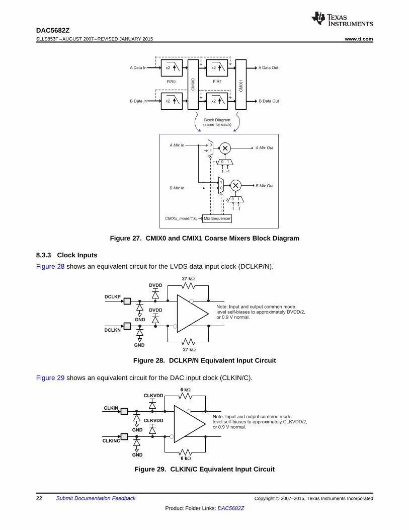
Figure 27. CMIX0 and CMIX1 Coarse Mixers Block Diagram
8.3.3 Clock InputsFigure 28 shows an equivalent circuit for the LVDS data input clock (DCLKP/N).
Figure 28. DCLKP/N Equivalent Input Circuit
Figure 29 shows an equivalent circuit for the DAC input clock (CLKIN/C).
Figure 29. CLKIN/C Equivalent Input Circuit
22 Submit Documentation Feedback Copyright © 2007–2015, Texas Instruments Incorporated
Product Folder Links: DAC5682Z
VTT
RPU RPD
0.01 µF
0.01 µF
100
CLKIN
CLKINC
CAC
Differential ECL or (LV)PECL
Source
RPU and RPD are chosen based on the clock driver
DAC5682Zwww.ti.com SLLS853F –AUGUST 2007–REVISED JANUARY 2015
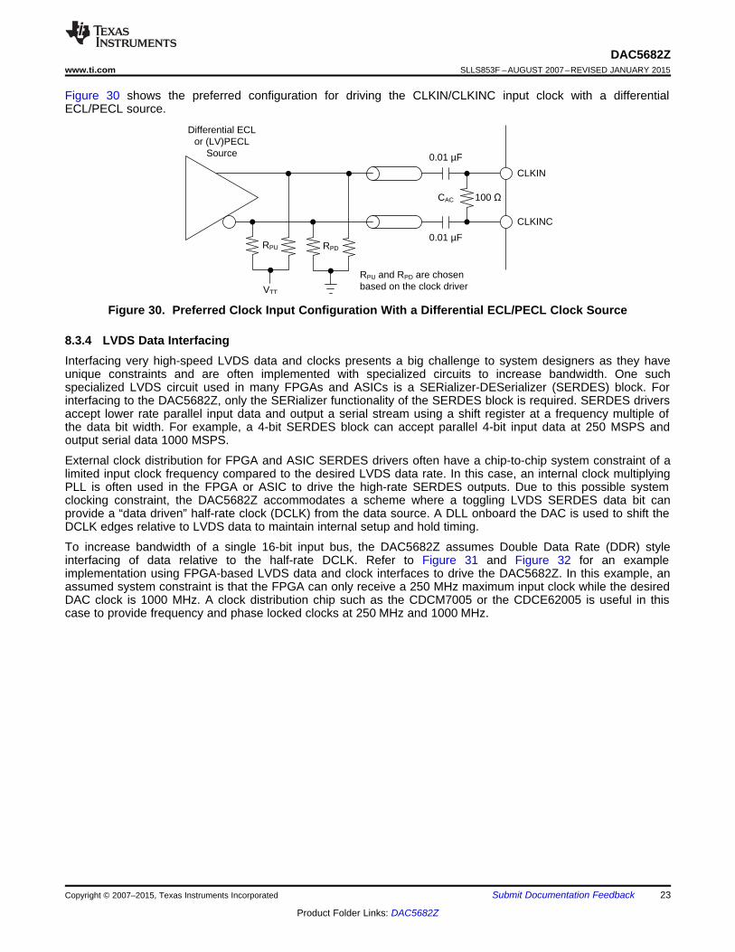
Figure 30 shows the preferred configuration for driving the CLKIN/CLKINC input clock with a differentialECL/PECL source.
Figure 30. Preferred Clock Input Configuration With a Differential ECL/PECL Clock Source
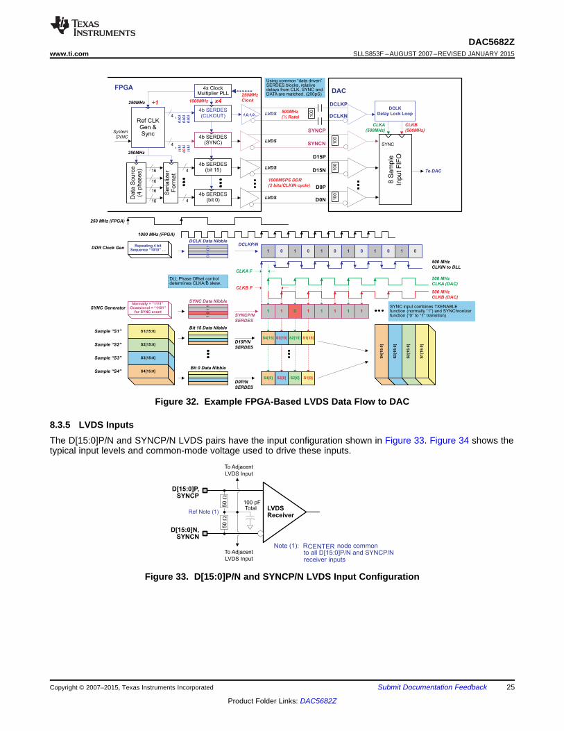
8.3.4 LVDS Data InterfacingInterfacing very high-speed LVDS data and clocks presents a big challenge to system designers as they haveunique constraints and are often implemented with specialized circuits to increase bandwidth. One suchspecialized LVDS circuit used in many FPGAs and ASICs is a SERializer-DESerializer (SERDES) block. Forinterfacing to the DAC5682Z, only the SERializer functionality of the SERDES block is required. SERDES driversaccept lower rate parallel input data and output a serial stream using a shift register at a frequency multiple ofthe data bit width. For example, a 4-bit SERDES block can accept parallel 4-bit input data at 250 MSPS andoutput serial data 1000 MSPS.
External clock distribution for FPGA and ASIC SERDES drivers often have a chip-to-chip system constraint of alimited input clock frequency compared to the desired LVDS data rate. In this case, an internal clock multiplyingPLL is often used in the FPGA or ASIC to drive the high-rate SERDES outputs. Due to this possible systemclocking constraint, the DAC5682Z accommodates a scheme where a toggling LVDS SERDES data bit canprovide a “data driven” half-rate clock (DCLK) from the data source. A DLL onboard the DAC is used to shift theDCLK edges relative to LVDS data to maintain internal setup and hold timing.
To increase bandwidth of a single 16-bit input bus, the DAC5682Z assumes Double Data Rate (DDR) styleinterfacing of data relative to the half-rate DCLK. Refer to Figure 31 and Figure 32 for an exampleimplementation using FPGA-based LVDS data and clock interfaces to drive the DAC5682Z. In this example, anassumed system constraint is that the FPGA can only receive a 250 MHz maximum input clock while the desiredDAC clock is 1000 MHz. A clock distribution chip such as the CDCM7005 or the CDCE62005 is useful in thiscase to provide frequency and phase locked clocks at 250 MHz and 1000 MHz.
Copyright © 2007–2015, Texas Instruments Incorporated Submit Documentation Feedback 23
Product Folder Links: DAC5682Z
VCON-Divider
ChargePumpR-
Div
Status & Control
PFD
10 MHzREFOSC
REF_IN
CL
K
DA
TA
ST
RB
CH
IP_
EN
PD
_B
UF
CPOUT
VCTRL_IN
900
TRF3703 AQM
DAC
DAC
LPF
Q-F
IR1 C
MIX
1I-F
IR1
CM
IX0
Q-F
IR0
I-F
IR0
FIF
O&
De
mu
x
100
100
100
100 Control
SD
IO
SD
O
SD
EN
B
SC
LK
RE
SE
TB
CL
KP
opt.PLL
LoopFilter
DLL
10
0
DAC5682Z DAC
PLLSynth
TRF3761-X PLL/VCO
LoopFilter
÷1÷4
Status &Control
LE
DA
TA
CL
K
PD
#
RE
SE
T#
VCXO
CL
KP
LoopFilter
Div1/2/4
Clock Divider /Distribution
VCXO_STATUS
REF_STATUS
PLL_LOCK
LO
CK
_D
ET
CDCM7005
5V
5V
SERDES
100
DAC5682ZControl
1.0 GHz250 MHz
1000 MHz
~ 2.1 GHz
TermT
erm
Pa
ralle
lto
SE
RD
ES
Fo
rma
tte
r
SERDES
SERDES
SERDES
DCLK
SYNC
D0
D15
DLL
CDCM7005Control
TRF3761-XControl
FPGA / ASIC
500 MHz
Toggling
Data Bit
1.0 GBPS
(DDR)
4x ClockMultiplier
1.0 GHz
25
0M
Hz
TX
Da
taS
ou
rce
PA
Du
ple
xe
r
Antenna
To TX
Feedback
To RX
Path
LPF
I
Q
I-Signal
Q-Signal
Freq/Phase Locked
Term
Term
DAC5682ZSLLS853F –AUGUST 2007–REVISED JANUARY 2015 www.ti.com
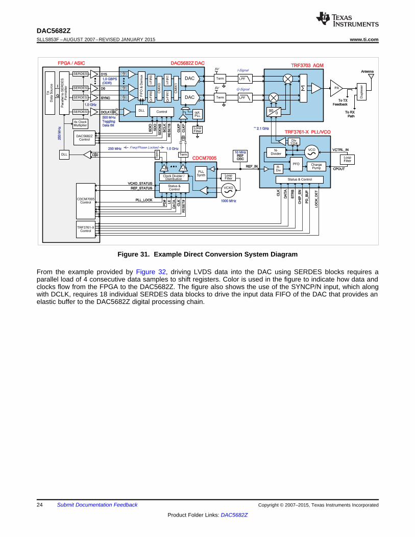
Figure 31. Example Direct Conversion System Diagram
From the example provided by Figure 32, driving LVDS data into the DAC using SERDES blocks requires aparallel load of 4 consecutive data samples to shift registers. Color is used in the figure to indicate how data andclocks flow from the FPGA to the DAC5682Z. The figure also shows the use of the SYNCP/N input, which alongwith DCLK, requires 18 individual SERDES data blocks to drive the input data FIFO of the DAC that provides anelastic buffer to the DAC5682Z digital processing chain.
24 Submit Documentation Feedback Copyright © 2007–2015, Texas Instruments Incorporated
Product Folder Links: DAC5682Z
D[15:0]P,SYNCP
D[15:0]N,SYNCN
50
W
LVDSReceiver
100 pFTotal
To Adjacent
LVDS Input
To Adjacent
LVDS Input
Ref Note (1)
Note (1): RCENTER node commonto all D[15:0]P/N and SYNCP/Nreceiver inputs
50
W
DCLKP
8S
am
ple
Input
FIF
O
D0P
D0N
D15P
D15N
DCLKN
Da
taS
ourc
e(4
phase
s) 4
LVDS
LVDS
FPGADAC
500MHz
(½ Rate)
1000MSPS DDR
(2 bits/CLKIN cycle)
1000MHz
250MHz
DCLK
Delay Lock LoopLVDS
4b SERDES(bit 0)4
10
010
0
4b SERDES(CLKOUT)
x4
4b SERDES(bit 15)
1,0,1,0...
SYNCP
SYNCNLVDS 1
004b SERDES
(SYNC)
Ref CLKGen &Sync
250MHz ÷1
System
SYNC
SYNC
4x ClockMultiplier PLL
4
4
101
0
101
0
101
0
“
16
16
Serializ
er
Form
at
16
16
D15P/N
SERDES
S2[15]S3[15]S4[15]
S1[0]S2[0]S3[0]S4[0]
Sample “S1”
Sample “S2”
Sample “S3”
Sample “S4”
S1[15]
S1[15:0]
S2[15:0]
S3[15:0]
S4[15:0]
S4
[15
:0]
S3
[15
:0]
S2
[15
:0]
S1
[15
:0]
250 MHz (FPGA)
1000 MHz (FPGA)
CLKB
(500MHz)
To DAC
250MHz
Clock
1 DCLKP/N
101 001
0
101 0
500 MHz
CLKB (DAC)
101 0
Bit 15 Data Nibble
Bit 0 Data Nibble
11
0
Repeating 4 bitSequence “1010” …
Normally = “1111”Ocassional = “1101”
for SYNC event
DDR Clock Gen
SYNC Generator01 1 1 1 1 1 1
Using common “data driven”SERDES blocks, relativedelays from CLK, SYNC andDATA are matched. (200pS)
1
DCLK Data Nibble
SYNC Data Nibble
500 MHz
CLKA (DAC)
CLKA
(500MHz)
DLL Phase Offset controldetermines CLKA/B skew.
1111
11
01
1111
“
D0P/N
SERDES
SYNCP/N
SERDES
CLKA F
CLKB F
500 MHz
CLKIN to DLL
SYNC input combines TXENABLEfunction (normally “1”) and SYNChronizerfunction (“0” to “1” transition)
10
0
DAC5682Zwww.ti.com SLLS853F –AUGUST 2007–REVISED JANUARY 2015
Figure 32. Example FPGA-Based LVDS Data Flow to DAC
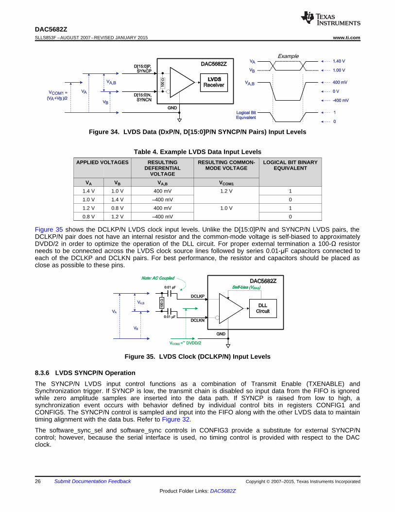
8.3.5 LVDS InputsThe D[15:0]P/N and SYNCP/N LVDS pairs have the input configuration shown in Figure 33. Figure 34 shows thetypical input levels and common-mode voltage used to drive these inputs.
Figure 33. D[15:0]P/N and SYNCP/N LVDS Input Configuration
Copyright © 2007–2015, Texas Instruments Incorporated Submit Documentation Feedback 25
Product Folder Links: DAC5682Z
DCLKP
10
0W
DLL
Circuit
DAC5682Z
DCLKN
GND
VCOM2 =~ DVDD/2
0.01 Fm Self-bias (VBIAS)
V
V
B
A,B
VA
Note: AC Coupled
0.01 Fm
D[15:0]P,SYNCP
10
0W LVDS
Receiver
DAC5682Z
D[15:0]N,SYNCN
GND
VCOM1 =
(VA+VB)/2VB
VA,B
VA
VA
VB
Logical BitEquivalent
1.40 V
1.00 V
400 mV
0 V
-400 mV
1
0
Example
VA,B
DAC5682ZSLLS853F –AUGUST 2007–REVISED JANUARY 2015 www.ti.com
Figure 34. LVDS Data (DxP/N, D[15:0]P/N SYNCP/N Pairs) Input Levels
Table 4. Example LVDS Data Input LevelsAPPLIED VOLTAGES RESULTING RESULTING COMMON- LOGICAL BIT BINARY
DEFERENTIAL MODE VOLTAGE EQUIVALENTVOLTAGE
VA VB VA,B VCOM1
1.4 V 1.0 V 400 mV 1.2 V 11.0 V 1.4 V –400 mV 01.2 V 0.8 V 400 mV 1.0 V 10.8 V 1.2 V –400 mV 0
Figure 35 shows the DCLKP/N LVDS clock input levels. Unlike the D[15:0]P/N and SYNCP/N LVDS pairs, theDCLKP/N pair does not have an internal resistor and the common-mode voltage is self-biased to approximatelyDVDD/2 in order to optimize the operation of the DLL circuit. For proper external termination a 100-Ω resistorneeds to be connected across the LVDS clock source lines followed by series 0.01-μF capacitors connected toeach of the DCLKP and DCLKN pairs. For best performance, the resistor and capacitors should be placed asclose as possible to these pins.
Figure 35. LVDS Clock (DCLKP/N) Input Levels
8.3.6 LVDS SYNCP/N OperationThe SYNCP/N LVDS input control functions as a combination of Transmit Enable (TXENABLE) andSynchronization trigger. If SYNCP is low, the transmit chain is disabled so input data from the FIFO is ignoredwhile zero amplitude samples are inserted into the data path. If SYNCP is raised from low to high, asynchronization event occurs with behavior defined by individual control bits in registers CONFIG1 andCONFIG5. The SYNCP/N control is sampled and input into the FIFO along with the other LVDS data to maintaintiming alignment with the data bus. Refer to Figure 32.
The software_sync_sel and software_sync controls in CONFIG3 provide a substitute for external SYNCP/Ncontrol; however, because the serial interface is used, no timing control is provided with respect to the DACclock.
26 Submit Documentation Feedback Copyright © 2007–2015, Texas Instruments Incorporated
Product Folder Links: DAC5682Z
SDIO
SCLK
internal
digital in
IOVDD
IOGND
RESETB
SDENB
internal
digital in
IOVDD
IOGND
DAC5682Zwww.ti.com SLLS853F –AUGUST 2007–REVISED JANUARY 2015
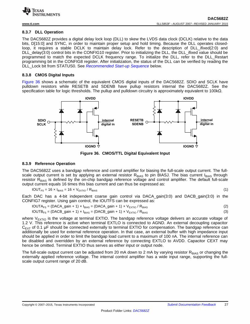
8.3.7 DLL OperationThe DAC5682Z provides a digital delay lock loop (DLL) to skew the LVDS data clock (DCLK) relative to the databits, D[15:0] and SYNC, in order to maintain proper setup and hold timing. Because the DLL operates closed-loop, it requires a stable DCLK to maintain delay lock. Refer to the description of DLL_ifixed(2:0) andDLL_delay(3:0) control bits in the CONFIG10 register. Prior to initializing the DLL, the DLL_ifixed value should beprogrammed to match the expected DCLK frequency range. To initialize the DLL, refer to the DLL_Restartprogramming bit in the CONFIG8 register. After initialization, the status of the DLL can be verified by reading theDLL_Lock bit from STATUS0. See Recommended Start-up Sequence below.
8.3.8 CMOS Digital InputsFigure 36 shows a schematic of the equivalent CMOS digital inputs of the DAC5682Z. SDIO and SCLK havepulldown resistors while RESETB and SDENB have pullup resistors internal the DAC5682Z. See thespecification table for logic thresholds. The pullup and pulldown circuitry is approximately equivalent to 100kΩ.
Figure 36. CMOS/TTL Digital Equivalent Input
8.3.9 Reference OperationThe DAC5682Z uses a bandgap reference and control amplifier for biasing the full-scale output current. The full-scale output current is set by applying an external resistor RBIAS to pin BIASJ. The bias current IBIAS throughresistor RBIAS is defined by the on-chip bandgap reference voltage and control amplifier. The default full-scaleoutput current equals 16 times this bias current and can thus be expressed as:
IOUTFS = 16 × IBIAS = 16 × VEXTIO / RBIAS (1)
Each DAC has a 4-bit independent coarse gain control via DACA_gain(3:0) and DACB_gain(3:0) in theCONFIG7 register. Using gain control, the IOUTFS can be expressed as:
IOUTAFS = (DACA_gain + 1) × IBIAS = (DACA_gain + 1) × VEXTIO / RBIAS (2)IOUTBFS = (DACB_gain + 1) × IBIAS = (DACB_gain + 1) × VEXTIO / RBIAS (3)
where VEXTIO is the voltage at terminal EXTIO. The bandgap reference voltage delivers an accurate voltage of1.2 V. This reference is active when terminal EXTLO is connected to AGND. An external decoupling capacitorCEXT of 0.1 μF should be connected externally to terminal EXTIO for compensation. The bandgap reference canadditionally be used for external reference operation. In that case, an external buffer with high impedance inputshould be applied in order to limit the bandgap load current to a maximum of 100 nA. The internal reference canbe disabled and overridden by an external reference by connecting EXTLO to AVDD. Capacitor CEXT mayhence be omitted. Terminal EXTIO thus serves as either input or output node.
The full-scale output current can be adjusted from 20 mA down to 2 mA by varying resistor RBIAS or changing theexternally applied reference voltage. The internal control amplifier has a wide input range, supporting the full-scale output current range of 20 dB.
Copyright © 2007–2015, Texas Instruments Incorporated Submit Documentation Feedback 27
Product Folder Links: DAC5682Z
DAC5682ZSLLS853F –AUGUST 2007–REVISED JANUARY 2015 www.ti.com
8.3.10 DAC Transfer FunctionThe CMOS DAC’s consist of a segmented array of NMOS current sinks, capable of sinking a full-scale outputcurrent up to 20 mA. Differential current switches direct the current to either one of the complementary outputnodes IOUT1 or IOUT2. (DACA = IOUTA1 or IOUTA2 and DACB = IOUTB1 or IOUTB2.) Complementary outputcurrents enable differential operation, thus canceling out common mode noise sources (digital feed-through, on-chip and PCB noise), dc offsets, even order distortion components, and increasing signal output power by afactor of two.
The full-scale output current is set using external resistor RBIAS in combination with an on-chip bandgap voltagereference source (+1.2 V) and control amplifier. Current IBIAS through resistor RBIAS is mirrored internally toprovide a maximum full-scale output current equal to 16 times IBIAS.
The relation between IOUT1 and IOUT2 can be expressed as:IOUT1 = – IOUTFS – IOUT2 (4)
We will denote current flowing into a node as – current and current flowing out of a node as + current. Becausethe output stage is a current sink the current can only flow from AVDD into the IOUT1 and IOUT2 pins. Theoutput current flow in each pin driving a resistive load can be expressed as:
IOUT1 = IOUTFS × (65536 – CODE) / 65536 (5)IOUT2 = IOUTFS × CODE / 65536 (6)
where CODE is the decimal representation of the DAC data input word.
For the case where IOUT1 and IOUT2 drive resistor loads RL directly, this translates into single ended voltagesat IOUT1 and IOUT2:
VOUT1 = AVDD – | IOUT1 | × RL (7)VOUT2 = AVDD – | IOUT2 | × RL (8)
Assuming that the data is full scale (65536 in offset binary notation) and the RL is 25 Ω, the differential voltagebetween pins IOUT1 and IOUT2 can be expressed as:
VOUT1 = AVDD – | –0 mA | × 25 Ω = 3.3 V (9)VOUT2 = AVDD – | –20 mA | × 25 Ω = 2.8 V (10)VDIFF = VOUT1 – VOUT2 = 0.5 V (11)
Do not exceed the compliance voltages at node IOUT1 and IOUT2, which would lead to increased signaldistortion.
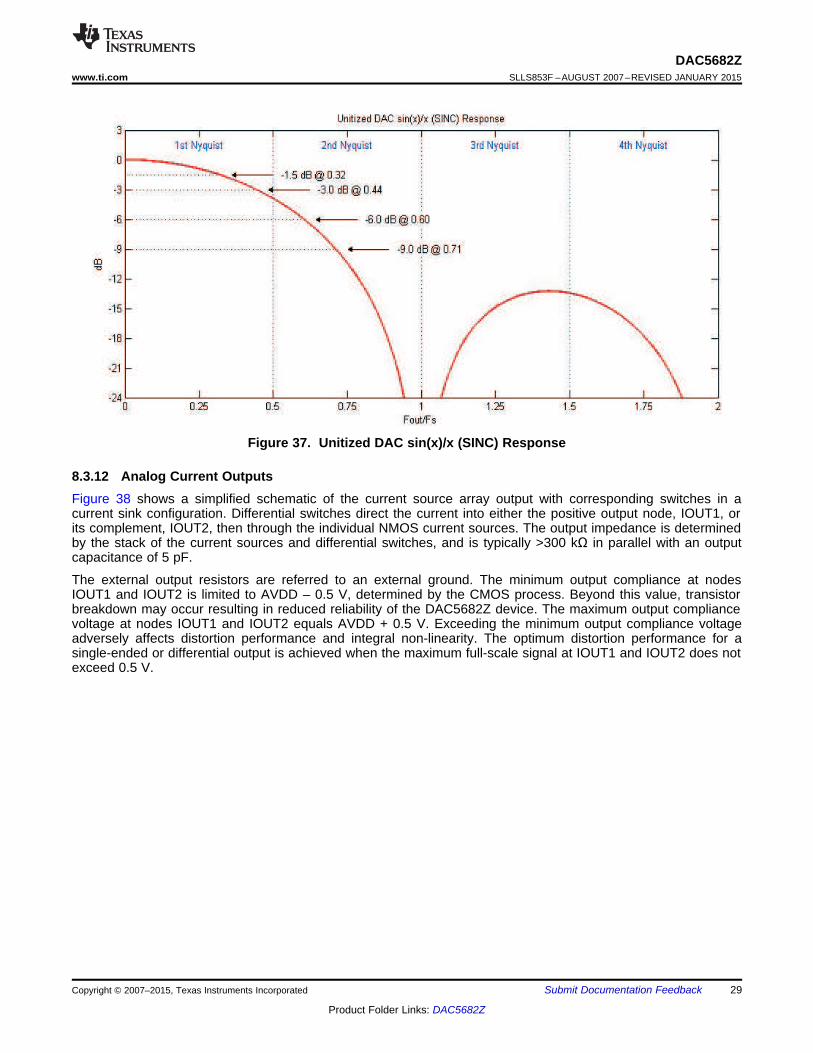
8.3.11 DAC Output SINC ResponseDue to sampled nature of a high-speed DAC, the well known sin(x)/x (or SINC) response can significantlyattenuate higher frequency output signals. See the Figure 37 which shows the unitized SINC attenuation roll-offwith respect to the final DAC sample rate in 4 Nyquist zones. For example, if the final DAC sample rate FS = 1.0GSPS, then a tone at 440MHz is attenuated by 3.0dB. Although the SINC response can create challenges infrequency planning, one side benefit is the natural attenuation of Nyquist images. The increased over-samplingratio of the input data provided by the 2x and 4x digital interpolation modes of the DAC5682Z improve the SINCroll-off (droop) within the band of interest of the original signal.
28 Submit Documentation Feedback Copyright © 2007–2015, Texas Instruments Incorporated
Product Folder Links: DAC5682Z
DAC5682Zwww.ti.com SLLS853F –AUGUST 2007–REVISED JANUARY 2015
Figure 37. Unitized DAC sin(x)/x (SINC) Response
8.3.12 Analog Current OutputsFigure 38 shows a simplified schematic of the current source array output with corresponding switches in acurrent sink configuration. Differential switches direct the current into either the positive output node, IOUT1, orits complement, IOUT2, then through the individual NMOS current sources. The output impedance is determinedby the stack of the current sources and differential switches, and is typically >300 kΩ in parallel with an outputcapacitance of 5 pF.
The external output resistors are referred to an external ground. The minimum output compliance at nodesIOUT1 and IOUT2 is limited to AVDD – 0.5 V, determined by the CMOS process. Beyond this value, transistorbreakdown may occur resulting in reduced reliability of the DAC5682Z device. The maximum output compliancevoltage at nodes IOUT1 and IOUT2 equals AVDD + 0.5 V. Exceeding the minimum output compliance voltageadversely affects distortion performance and integral non-linearity. The optimum distortion performance for asingle-ended or differential output is achieved when the maximum full-scale signal at IOUT1 and IOUT2 does notexceed 0.5 V.
Copyright © 2007–2015, Texas Instruments Incorporated Submit Documentation Feedback 29
Product Folder Links: DAC5682Z
IOUT11 : 1
IOUT2
AVDD (3.3 V)
50 W
100 W
50 W
AVDD (3.3 V)
R
50
LOAD
W
RLOADRLOAD
AVDD
S(1)
S(1)C
S(2)
S(2)C
S(N)
S(N)C
...
IOUT1 IOUT2
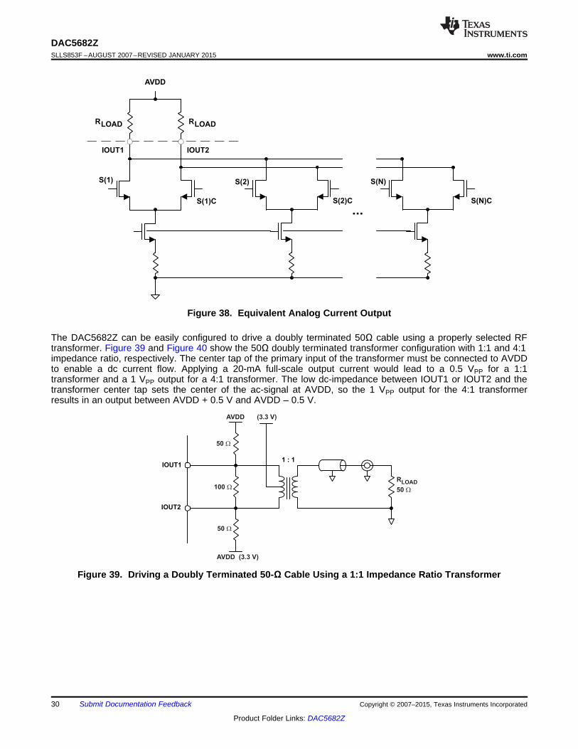
DAC5682ZSLLS853F –AUGUST 2007–REVISED JANUARY 2015 www.ti.com
Figure 38. Equivalent Analog Current Output
The DAC5682Z can be easily configured to drive a doubly terminated 50Ω cable using a properly selected RFtransformer. Figure 39 and Figure 40 show the 50Ω doubly terminated transformer configuration with 1:1 and 4:1impedance ratio, respectively. The center tap of the primary input of the transformer must be connected to AVDDto enable a dc current flow. Applying a 20-mA full-scale output current would lead to a 0.5 VPP for a 1:1transformer and a 1 VPP output for a 4:1 transformer. The low dc-impedance between IOUT1 or IOUT2 and thetransformer center tap sets the center of the ac-signal at AVDD, so the 1 VPP output for the 4:1 transformerresults in an output between AVDD + 0.5 V and AVDD – 0.5 V.
Figure 39. Driving a Doubly Terminated 50-Ω Cable Using a 1:1 Impedance Ratio Transformer
30 Submit Documentation Feedback Copyright © 2007–2015, Texas Instruments Incorporated
Product Folder Links: DAC5682Z
( )t t ´ t tæ ö
t ç ÷t t t t tè ø
22 1 2 3
C1 = 1 1 - C2 = R1 =3 3 1 3 - 2
IOUT1
4 : 1
IOUT2
AVDD (3.3 V)
100 W
100 W
AVDD (3.3 V)
R
50
LOAD
W
DAC5682Zwww.ti.com SLLS853F –AUGUST 2007–REVISED JANUARY 2015
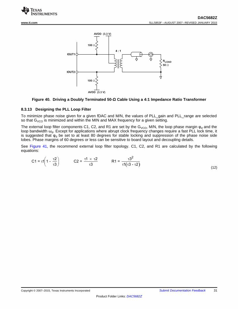
Figure 40. Driving a Doubly Terminated 50-Ω Cable Using a 4:1 Impedance Ratio Transformer
8.3.13 Designing the PLL Loop FilterTo minimize phase noise given for a given fDAC and M/N, the values of PLL_gain and PLL_range are selectedso that GVCO is minimized and within the MIN and MAX frequency for a given setting.
The external loop filter components C1, C2, and R1 are set by the GVCO, M/N, the loop phase margin φd and theloop bandwidth ωd. Except for applications where abrupt clock frequency changes require a fast PLL lock time, itis suggested that φd be set to at least 80 degrees for stable locking and suppression of the phase noise sidelobes. Phase margins of 60 degrees or less can be sensitive to board layout and decoupling details.
See Figure 41, the recommend external loop filter topology. C1, C2, and R1 are calculated by the followingequations:
(12)
Copyright © 2007–2015, Texas Instruments Incorporated Submit Documentation Feedback 31
Product Folder Links: DAC5682Z
DAC-A
DAC-B
Q-F
IR1 C
MIX
1I-F
IR1
CM
IX0
Q-F
IR0
I-F
IR0
FIF
O&
De
mu
x
100
100
100
100
CL
KIN
opt.PLL
LoopFilter
DLL
DAC5682Z DAC
CL
KIN
C
CDCM7005
DCLK
SYNC
D0
D15
Agilent 81205A
ParBERT
PatternMemory
100
Opt.Clock
Divider
DAC5682ZEVM
Sta
ckin
gIn
terf
ace
Co
nn
ecto
r
DAC5682ZEVM SMA Adapter Board
100
100
100
100
3.3 V
3.3 V
3.3 V
3.3 V
3.3 V
3.3 V
Agilent 8133APulse Generator
OptionalDivider HP8665B
SynthesizedSignal
Generator
P
N
P
N
P
N
P
N
Rohde &SchwartzFSUSpectrumAnalyzer
36 eachSMA-SMA cables
Swap CableFor DAC-Bmeasurements
Sp
litte
r
PLLExternalLoopFilter
LPF(Pin 64)
DAC5682Z PLL
C2 C1
R1
( )( )
VCOK K tan Φ + sec Φ1d d d1 = tan Φ + sec Φ 2 = 3 =d d
2 tan Φ + sec Φ dd d dd
t t twww
DAC5682ZSLLS853F –AUGUST 2007–REVISED JANUARY 2015 www.ti.com
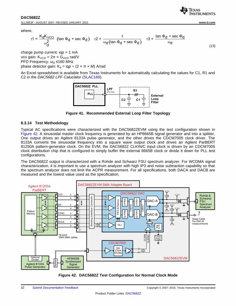
where,
(13)
charge pump current: iqp = 1 mAvco gain: KVCO = 2π × GVCO rad/VPFD Frequency: ωd ≤160 MHzphase detector gain: Kd = iqp ÷ (2 × π × M) A/rad
An Excel spreadsheet is available from Texas Instruments for automatically calculating the values for C1, R1 andC2 in the DAC5682 LPF Caluclator (SLAC169).
Figure 41. Recommended External Loop Filter Topology
8.3.14 Test MethodologyTypical AC specifications were characterized with the DAC5682ZEVM using the test configuration shown inFigure 42. A sinusoidal master clock frequency is generated by an HP8665B signal generator and into a splitter.One output drives an Agilent 8133A pulse generator, and the other drives the CDCM7005 clock driver. The8133A converts the sinusoidal frequency into a square wave output clock and drives an Agilent ParBERT81250A pattern-generator clock. On the EVM, the DAC5682Z CLKIN/C input clock is driven by an CDCM7005clock distribution chip that is configured to simply buffer the external 8665B clock or divide it down for PLL testconfigurations.
The DAC5682Z output is characterized with a Rohde and Schwarz FSU spectrum analyzer. For WCDMA signalcharacterization, it is important to use a spectrum analyzer with high IP3 and noise subtraction capability so thatthe spectrum analyzer does not limit the ACPR measurement. For all specifications, both DACA and DACB aremeasured and the lowest value used as the specification.
Figure 42. DAC5682Z Test Configuration for Normal Clock Mode
32 Submit Documentation Feedback Copyright © 2007–2015, Texas Instruments Incorporated
Product Folder Links: DAC5682Z
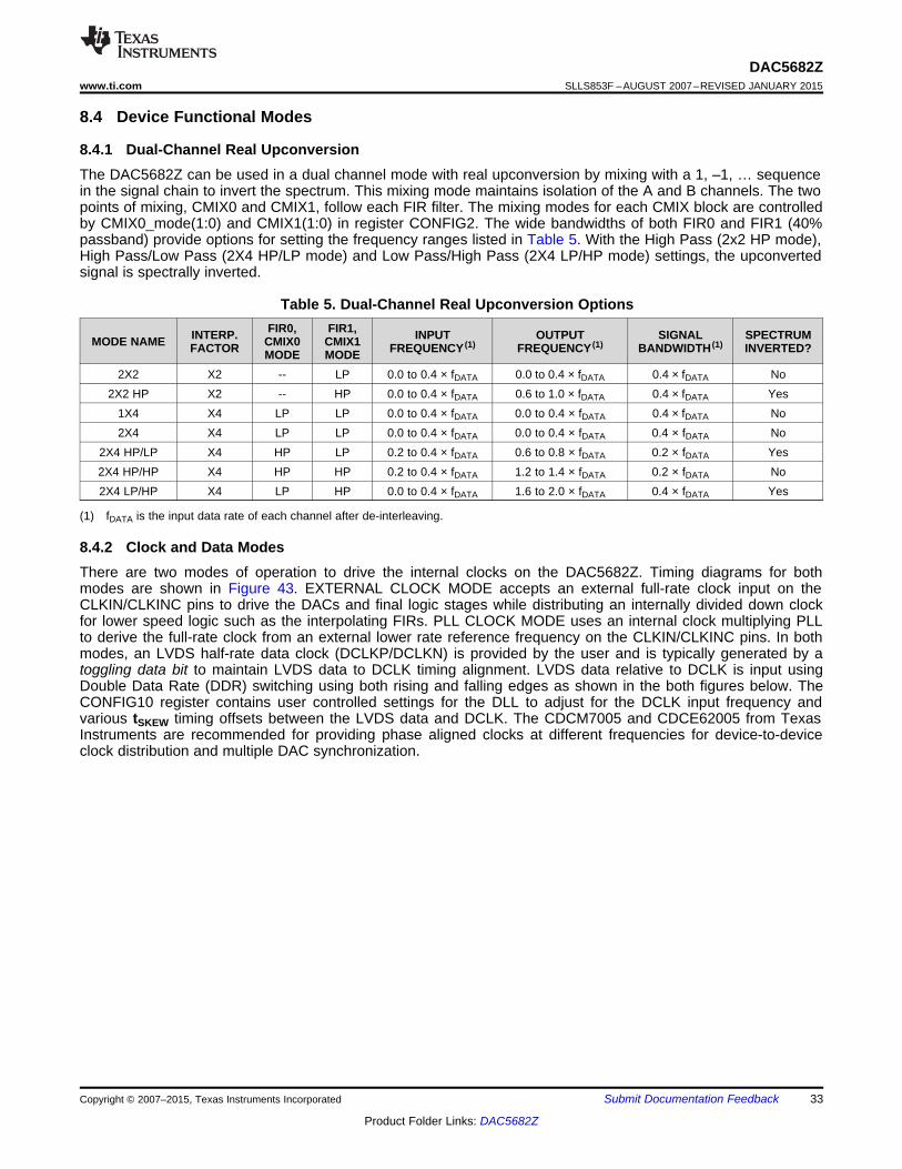
DAC5682Zwww.ti.com SLLS853F –AUGUST 2007–REVISED JANUARY 2015
8.4 Device Functional Modes
8.4.1 Dual-Channel Real UpconversionThe DAC5682Z can be used in a dual channel mode with real upconversion by mixing with a 1, –1, … sequencein the signal chain to invert the spectrum. This mixing mode maintains isolation of the A and B channels. The twopoints of mixing, CMIX0 and CMIX1, follow each FIR filter. The mixing modes for each CMIX block are controlledby CMIX0_mode(1:0) and CMIX1(1:0) in register CONFIG2. The wide bandwidths of both FIR0 and FIR1 (40%passband) provide options for setting the frequency ranges listed in Table 5. With the High Pass (2x2 HP mode),High Pass/Low Pass (2X4 HP/LP mode) and Low Pass/High Pass (2X4 LP/HP mode) settings, the upconvertedsignal is spectrally inverted.
Table 5. Dual-Channel Real Upconversion OptionsFIR0, FIR1,INTERP. INPUT OUTPUT SIGNAL SPECTRUMMODE NAME CMIX0 CMIX1FACTOR FREQUENCY (1) FREQUENCY (1) BANDWIDTH (1) INVERTED?MODE MODE
2X2 X2 -- LP 0.0 to 0.4 × fDATA 0.0 to 0.4 × fDATA 0.4 × fDATA No2X2 HP X2 -- HP 0.0 to 0.4 × fDATA 0.6 to 1.0 × fDATA 0.4 × fDATA Yes
1X4 X4 LP LP 0.0 to 0.4 × fDATA 0.0 to 0.4 × fDATA 0.4 × fDATA No2X4 X4 LP LP 0.0 to 0.4 × fDATA 0.0 to 0.4 × fDATA 0.4 × fDATA No
2X4 HP/LP X4 HP LP 0.2 to 0.4 × fDATA 0.6 to 0.8 × fDATA 0.2 × fDATA Yes2X4 HP/HP X4 HP HP 0.2 to 0.4 × fDATA 1.2 to 1.4 × fDATA 0.2 × fDATA No2X4 LP/HP X4 LP HP 0.0 to 0.4 × fDATA 1.6 to 2.0 × fDATA 0.4 × fDATA Yes
(1) fDATA is the input data rate of each channel after de-interleaving.
8.4.2 Clock and Data ModesThere are two modes of operation to drive the internal clocks on the DAC5682Z. Timing diagrams for bothmodes are shown in Figure 43. EXTERNAL CLOCK MODE accepts an external full-rate clock input on theCLKIN/CLKINC pins to drive the DACs and final logic stages while distributing an internally divided down clockfor lower speed logic such as the interpolating FIRs. PLL CLOCK MODE uses an internal clock multiplying PLLto derive the full-rate clock from an external lower rate reference frequency on the CLKIN/CLKINC pins. In bothmodes, an LVDS half-rate data clock (DCLKP/DCLKN) is provided by the user and is typically generated by atoggling data bit to maintain LVDS data to DCLK timing alignment. LVDS data relative to DCLK is input usingDouble Data Rate (DDR) switching using both rising and falling edges as shown in the both figures below. TheCONFIG10 register contains user controlled settings for the DLL to adjust for the DCLK input frequency andvarious tSKEW timing offsets between the LVDS data and DCLK. The CDCM7005 and CDCE62005 from TexasInstruments are recommended for providing phase aligned clocks at different frequencies for device-to-deviceclock distribution and multiple DAC synchronization.
Copyright © 2007–2015, Texas Instruments Incorporated Submit Documentation Feedback 33
Product Folder Links: DAC5682Z
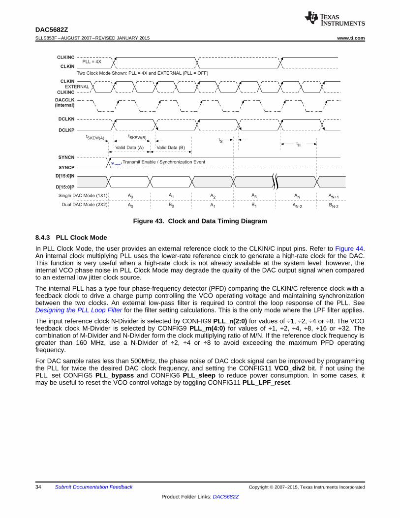
CLKINC
CLKIN
Two Clock Mode Shown: PLL = 4X and EXTERNAL (PLL = OFF)
PLL = 4X
CLKINC
CLKIN
EXTERNAL
DACCLK(Internal)
DCLKN
DCLKP
tSKEW(A)tSKEW(B)
Valid Data (A) Valid Data (B)
Transmit Enable / Synchronization EventSYNCN
SYNCP
D[15:0]N
D[15:0]P
Single DAC Mode (1X1)
Dual DAC Mode (2X2)
A0
A0
A1
B0
A2
A1
A3
B1
AN
AN-2
AN+1
BN-2
tStH
DAC5682ZSLLS853F –AUGUST 2007–REVISED JANUARY 2015 www.ti.com
Figure 43. Clock and Data Timing Diagram
8.4.3 PLL Clock ModeIn PLL Clock Mode, the user provides an external reference clock to the CLKIN/C input pins. Refer to Figure 44.An internal clock multiplying PLL uses the lower-rate reference clock to generate a high-rate clock for the DAC.This function is very useful when a high-rate clock is not already available at the system level; however, theinternal VCO phase noise in PLL Clock Mode may degrade the quality of the DAC output signal when comparedto an external low jitter clock source.
The internal PLL has a type four phase-frequency detector (PFD) comparing the CLKIN/C reference clock with afeedback clock to drive a charge pump controlling the VCO operating voltage and maintaining synchronizationbetween the two clocks. An external low-pass filter is required to control the loop response of the PLL. SeeDesigning the PLL Loop Filter for the filter setting calculations. This is the only mode where the LPF filter applies.
The input reference clock N-Divider is selected by CONFIG9 PLL_n(2:0) for values of ÷1, ÷2, ÷4 or ÷8. The VCOfeedback clock M-Divider is selected by CONFIG9 PLL_m(4:0) for values of ÷1, ÷2, ÷4, ÷8, ÷16 or ÷32. Thecombination of M-Divider and N-Divider form the clock multiplying ratio of M/N. If the reference clock frequency isgreater than 160 MHz, use a N-Divider of ÷2, ÷4 or ÷8 to avoid exceeding the maximum PFD operatingfrequency.
For DAC sample rates less than 500MHz, the phase noise of DAC clock signal can be improved by programmingthe PLL for twice the desired DAC clock frequency, and setting the CONFIG11 VCO_div2 bit. If not using thePLL, set CONFIG5 PLL_bypass and CONFIG6 PLL_sleep to reduce power consumption. In some cases, itmay be useful to reset the VCO control voltage by toggling CONFIG11 PLL_LPF_reset.
34 Submit Documentation Feedback Copyright © 2007–2015, Texas Instruments Incorporated
Product Folder Links: DAC5682Z
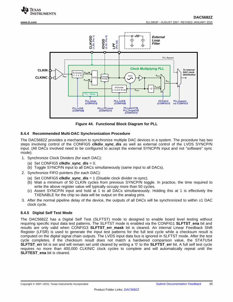
CLKIN
CLKINC
CL
KV
DD
(1.8
V,P
in1)
ChargePump
N–Divider
(1, 2, 4, 8)PFD
FVCOVCO
÷2
FPLL
M-Divider
( 1,2,4,8,16,32)
PLL Bypass
Clock Multiplying PLL
ExternalLoopFilter
To internalDAC clockdistribution
LP
F(P
in64
)
FVCO/M
FREF
FVCO
FREF/N
PLL Sleep
PLL_m(4:0)(CONFIG9)
PLL_n(2:0)(CONFIG9)
PLL_sleep(CONFIG6)
VCO_div2(CONFIG11)
PLL_gain(1:0),PLL_range(3:0)
(CONFIG11)
PLL_bypassvia CONFIG5
PLL_LPF_reset(CONFIG11)
FVCO/2
IOV
DD
(3.3
V,P
in9)
DAC5682Zwww.ti.com SLLS853F –AUGUST 2007–REVISED JANUARY 2015
Figure 44. Functional Block Diagram for PLL
8.4.4 Recommended Multi-DAC Synchronization ProcedureThe DAC5682Z provides a mechanism to synchronize multiple DAC devices in a system. The procedure has twosteps involving control of the CONFIG5 clkdiv_sync_dis as well as external control of the LVDS SYNCP/Ninput. (All DACs involved need to be configured to accept the external SYNCP/N input and not "software" syncmode).1. Synchronize Clock Dividers (for each DAC):
(a) Set CONFIG5 clkdiv_sync_dis = 0.(b) Toggle SYNCP/N input to all DACs simultaneously (same input to all DACs).
2. Synchronize FIFO pointers (for each DAC):(a) Set CONFIG5 clkdiv_sync_dis = 1 (Disable clock divider re-sync).(b) Wait a minimum of 50 CLKIN cycles from previous SYNCP/N toggle. In practice, the time required to
write the above register value will typically occupy more than 50 cycles.(c) Assert SYNCP/N input and hold at 1 to all DACs simultaneously. Holding this at 1 is effectively the
TXENABLE for the chip so data will be output on the analog pins.3. After the normal pipeline delay of the device, the outputs of all DACs will be synchronized to within ±1 DAC
clock cycle.
8.4.5 Digital Self Test ModeThe DAC5682Z has a Digital Self Test (SLFTST) mode to designed to enable board level testing withoutrequiring specific input data test patterns. The SLFTST mode is enabled via the CONFIG1 SLFTST_ena bit andresults are only valid when CONFIG3 SLFTST_err_mask bit is cleared. An internal Linear Feedback ShiftRegister (LFSR) is used to generate the input test patterns for the full test cycle while a checksum result iscomputed on the digital signal chain outputs. The LVDS input data bus is ignored in SLFTST mode. After the testcycle completes, if the checksum result does not match a hardwired comparison value, the STATUS4SLFTST_err bit is set and will remain set until cleared by writing a ‘0’ to the SLFTST_err bit. A full self test cyclerequires no more than 400,000 CLKIN/C clock cycles to complete and will automatically repeat until theSLFTEST_ena bit is cleared.
Copyright © 2007–2015, Texas Instruments Incorporated Submit Documentation Feedback 35
Product Folder Links: DAC5682Z
DAC5682ZSLLS853F –AUGUST 2007–REVISED JANUARY 2015 www.ti.com
To initiate a the Digital Self Test:1. Provide a normal CLKIN/C input clock. (The PLL is not used in SLFTST mode)2. Provide a RESETB pulse to perform a hardware reset on device.3. Program the registers with the values shown in Table 6. These register values contain the settings to
properly configure the SLFTST including SLFTST_ena and SLFTST_err_mask bits4. Provide a ‘1’ on the SYNCP/N input to initiate TXENABLE.5. Wait at a minimum of 400,000 CLKIN/C cycles for the SLFTST to complete. Example: If CLKIN = 1GHz, then
the wait period is 400,000 × 1 / 1GHz = 400 μSec.6. Read STATUS4 SLFTST_err bit. If set, a self test error has occurred. The SLFTST_err status may
optionally be programmed to output on the SDO pin if using the 3-bit SIF interface. See Table 6 Note (1).7. (Optional) The SLFTST function automatically repeats until SLFTST_ena bit is cleared. To the loop the test,
write a ‘0’ to STATUS4 SLFTST_err to clear previous errors and continue at step 5 above.8. To continue normal operating mode, provide another RESETB pulse and reprogram registers to the desired
normal settings.
Table 6. Digital Self Test (SLFTST) Register ValuesREGISTER ADDRESS (hex) VALUE (Binary) VALUE (Hex)CONFIG1 01 00011000 18CONFIG2 02 11101010 EACONFIG3 03 10110000 B0STATUS4 04 00000000 00CONFIG5 05 00000110 06CONFIG6 06 00001111 0F
CONFIG12 0C 00001010 0ACONFIG13 0D 01010101 55
CONFIG14 (1) 0E 00001010 0ACONFIG15 0F 10101010 AAAll others – Default Default
(1) If using a 3-bit SIF interface, the SDO pin can be programmed to report SLFTST_err status via the SDO_fun_sel(2:0) bits. In this case,set CONFIG14 = ‘10101010’ or AA hex.
8.5 Programming
8.5.1 Serial InterfaceThe serial port of the DAC5682Z is a flexible serial interface which communicates with industry standardmicroprocessors and microcontrollers. The interface provides read/write access to all registers used to define theoperating modes of DAC5682Z. It is compatible with most synchronous transfer formats and can be configuredas a 3 or 4 pin interface by SIF4 in register CONFIG5. In both configurations, SCLK is the serial interface inputclock and SDENB is serial interface enable. For 3 pin configuration, SDIO is a bidirectional pin for both data inand data out. For 4 pin configuration, SDIO is data in only and SDO is data out only. Data is input into the devicewith the rising edge of SCLK. Data is output from the device on the falling edge of SCLK.Each read/write operation is framed by signal SDENB (Serial Data Enable Bar) asserted low for 2 to 5 bytes,depending on the data length to be transferred (1–4 bytes). The first frame byte is the instruction cycle whichidentifies the following data transfer cycle as read or write, how many bytes to transfer, and what address totransfer the data. indicates the function of each bit in the instruction cycle and is followed by a detaileddescription of each bit. Frame bytes 2 to 5 comprise the data transfer cycle.
MSB LSBBit 7 6 5 4 3 2 1 0
Description R/W N1 N0 A4 A3 A2 A1 A0
36 Submit Documentation Feedback Copyright © 2007–2015, Texas Instruments Incorporated
Product Folder Links: DAC5682Z
Instruction Cycle Data Transfer Cycle (s)
SDENB
SCLK
SDIO
SDENB
SCLK
SDIO
r/w N1 N0 A4 A3 A2 A1 A0 D7 D6 D5 D4 D3 D2 D1 D0
t (SDENB)S tSCLK
t (SDIO)S
t (SDIO)htSCLKH
tSCLKL
DAC5682Zwww.ti.com SLLS853F –AUGUST 2007–REVISED JANUARY 2015
R/W Identifies the following data transfer cycle as a read or write operation. A high indicates a readoperation from DAC5682Z and a low indicates a write operation to DAC5682Z.
[N1 : N0] Identifies the number of data bytes to be transferred per Table 5 below. Data is transferred MSBfirst.
Table 7. Number of Transferred Bytes Within OneCommunication Frame
N1 N0 Description0 0 Transfer 1 Byte0 1 Transfer 2 Bytes1 0 Transfer 3 Bytes1 1 Transfer 4 Bytes
[A4 : A0] Identifies the address of the register to be accessed during the read or write operation. For multi-byte transfers, this address is the starting address. Note that the address is written to theDAC5682Z MSB first and counts down for each byte.
Figure 45 shows the serial interface timing diagram for a DAC5682Z write operation. SCLK is the serial interfaceclock input to DAC5682Z. Serial data enable SDENB is an active low input to DAC5682Z. SDIO is serial data in.Input data to DAC5682Z is clocked on the rising edges of SCLK.
Figure 45. Serial Interface Write Timing Diagram
Figure 46 shows the serial interface timing diagram for a DAC5682Z read operation. SCLK is the serial interfaceclock input to DAC5682Z. Serial data enable SDENB is an active low input to DAC5682Z. SDIO is serial data induring the instruction cycle. In 3 pin configuration, SDIO is data out from DAC5682Z during the data transfercycle(s), while SDO is in a high-impedance state. In 4 pin configuration, SDO is data out from DAC5682Z duringthe data transfer cycle(s). At the end of the data transfer, SDO will output low on the final falling edge of SCLKuntil the rising edge of SDENB when it will 3-state.
Copyright © 2007–2015, Texas Instruments Incorporated Submit Documentation Feedback 37
Product Folder Links: DAC5682Z
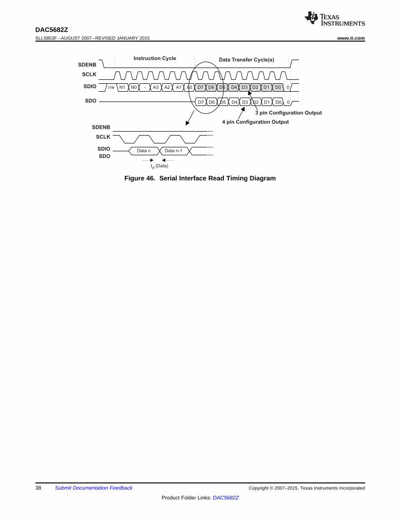
SDENB
SCLK
SDIO
SDO
SDENB
SCLK
SDIO
SDO
Instruction Cycle Data Transfer Cycle(s)
r/w N1 N0 - A3 A2 A1 A0 D7 D6 D5 D4 D3 D2 D1 D0 0
D7 D6 D5 D4 D3 D2 D1 D0 0
3 pin Configuration Output
4 pin Configuration Output
Data n Data n-1
t (Data)d
DAC5682ZSLLS853F –AUGUST 2007–REVISED JANUARY 2015 www.ti.com
Figure 46. Serial Interface Read Timing Diagram
38 Submit Documentation Feedback Copyright © 2007–2015, Texas Instruments Incorporated
Product Folder Links: DAC5682Z
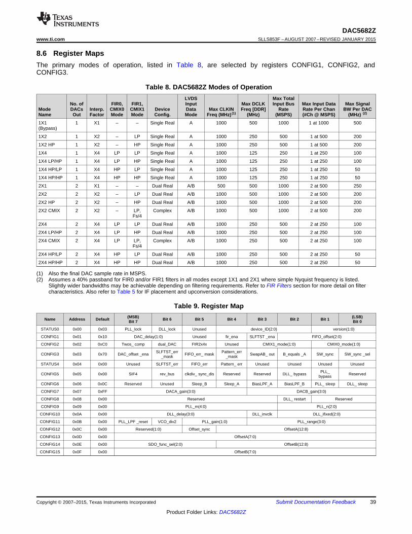
DAC5682Zwww.ti.com SLLS853F –AUGUST 2007–REVISED JANUARY 2015
8.6 Register MapsThe primary modes of operation, listed in Table 8, are selected by registers CONFIG1, CONFIG2, andCONFIG3.
Table 8. DAC5682Z Modes of OperationLVDS Max Total
No. of FIR0, FIR1, Input Max DCLK Input Bus Max Input Data Max SignalMode DACs Interp. CMIX0 CMIX1 Device Data Max CLKIN Freq [DDR] Rate Rate Per Chan BW Per DACName Out Factor Mode Mode Config. Mode Freq (MHz) (1) (MHz) (MSPS) (#Ch @ MSPS) (MHz) (2)
1X1 1 X1 – – Single Real A 1000 500 1000 1 at 1000 500(Bypass)
1X2 1 X2 – LP Single Real A 1000 250 500 1 at 500 200
1X2 HP 1 X2 – HP Single Real A 1000 250 500 1 at 500 200
1X4 1 X4 LP LP Single Real A 1000 125 250 1 at 250 100
1X4 LP/HP 1 X4 LP HP Single Real A 1000 125 250 1 at 250 100
1X4 HP/LP 1 X4 HP LP Single Real A 1000 125 250 1 at 250 50
1X4 HP/HP 1 X4 HP HP Single Real A 1000 125 250 1 at 250 50
2X1 2 X1 – – Dual Real A/B 500 500 1000 2 at 500 250
2X2 2 X2 – LP Dual Real A/B 1000 500 1000 2 at 500 200
2X2 HP 2 X2 – HP Dual Real A/B 1000 500 1000 2 at 500 200
2X2 CMIX 2 X2 – LP, Complex A/B 1000 500 1000 2 at 500 200Fs/4
2X4 2 X4 LP LP Dual Real A/B 1000 250 500 2 at 250 100
2X4 LP/HP 2 X4 LP HP Dual Real A/B 1000 250 500 2 at 250 100
2X4 CMIX 2 X4 LP LP, Complex A/B 1000 250 500 2 at 250 100Fs/4
2X4 HP/LP 2 X4 HP LP Dual Real A/B 1000 250 500 2 at 250 50
2X4 HP/HP 2 X4 HP HP Dual Real A/B 1000 250 500 2 at 250 50
(1) Also the final DAC sample rate in MSPS.(2) Assumes a 40% passband for FIR0 and/or FIR1 filters in all modes except 1X1 and 2X1 where simple Nyquist frequency is listed.
Slightly wider bandwidths may be achievable depending on filtering requirements. Refer to FIR Filters section for more detail on filtercharacteristics. Also refer to Table 5 for IF placement and upconversion considerations.
Table 9. Register Map(MSB) (LSB)Name Address Default Bit 6 Bit 5 Bit 4 Bit 3 Bit 2 Bit 1Bit 7 Bit 0
STATUS0 0x00 0x03 PLL_lock DLL_lock Unused device_ID(2:0) version(1:0)
CONFIG1 0x01 0x10 DAC_delay(1:0) Unused fir_ena SLFTST _ena FIFO_offset(2:0)
CONFIG2 0x02 0xC0 Twos_ comp dual_DAC FIR2x4x Unused CMIX1_mode(1:0) CMIX0_mode(1:0)
SLFTST_err Pattern_errCONFIG3 0x03 0x70 DAC_offset _ena FIFO_err_ mask SwapAB_ out B_equals _A SW_sync SW_sync _sel_mask _mask
STATUS4 0x04 0x00 Unused SLFTST_err FIFO_err Pattern_ err Unused Unused Unused Unused
PLL_CONFIG5 0x05 0x00 SIF4 rev_bus clkdiv_ sync_dis Reserved Reserved DLL_ bypass Reservedbypass
CONFIG6 0x06 0x0C Reserved Unused Sleep_B Sleep_A BiasLPF_A BiasLPF_B PLL_ sleep DLL_ sleep
CONFIG7 0x07 0xFF DACA_gain(3:0) DACB_gain(3:0)
CONFIG8 0x08 0x00 Reserved DLL_ restart Reserved
CONFIG9 0x09 0x00 PLL_m(4:0) PLL_n(2:0)
CONFIG10 0x0A 0x00 DLL_delay(3:0) DLL_invclk DLL_ifixed(2:0)
CONFIG11 0x0B 0x00 PLL_LPF _reset VCO_div2 PLL_gain(1:0) PLL_range(3:0)
CONFIG12 0x0C 0x00 Reserved(1:0) Offset_sync OffsetA(12:8)
CONFIG13 0x0D 0x00 OffsetA(7:0)
CONFIG14 0x0E 0x00 SDO_func_sel(2:0) OffsetB(12:8)
CONFIG15 0x0F 0x00 OffsetB(7:0)
Copyright © 2007–2015, Texas Instruments Incorporated Submit Documentation Feedback 39
Product Folder Links: DAC5682Z
DAC5682ZSLLS853F –AUGUST 2007–REVISED JANUARY 2015 www.ti.com
8.6.1 Register Name: STATUS0 – Address: 0x00, Default = 0x03
7 6 5 4 3 2 1 0PLL_lock DLL_lock Unused device_ID(2:0) version(1:0)
0 0 0 0 0 0 1 1
PLL_lock: Asserted when the internal PLL is locked. (Read Only)DLL_lock: Asserted when the internal DLL is locked. Once the DLL is locked, this bit should remain a
‘1’ unless the DCLK input clock is removed or abruptly changes frequency causing the DLLto fall out of lock. (Read Only)
device_ID(2:0): Returns ‘000’ for DAC5682Z Device_ID code. (ReadOnly)version(1:0): A hardwired register that contains the register set version of the chip. (ReadOnly)
version (1:0) Identification‘01’ PG1.0 Initial Register Set‘10’ PG1.1 Register Set‘11' Production Register Set
8.6.2 Register Name: CONFIG1 – Address: 0x01, Default = 0x10
7 6 5 4 3 2 1 0DAC_delay(1:0) Unused FIR_ena SLFTST_ena FIFO_offset(2:0)
0 0 0 1 0 0 0 0
DAC_delay(1:0): DAC data delay adjustment. (0–3 periods of the DAC clock) This can be used to adjustsystem level output timing. The same delay is applied to both DACA and DACB data paths.
FIR_ena: When set, the interpolation filters are enabled.SLFTST_ena: When set, a Digital Self Test (SLFTST) of the core logic is enabled. Refer to Digital Self
Test Mode for details on SLFTST operation.FIFO_offset(2:0): Programs the output pointer location of the FIFO, allowing the input pointer to be shifted –4
to +3 positions upon SYNC. Default offset is 0 and is updated upon each sync event.
FIFO_offset(2:0) Offset011 +3010 +2001 +1000 0111 –1110 –2101 –3100 –4
40 Submit Documentation Feedback Copyright © 2007–2015, Texas Instruments Incorporated
Product Folder Links: DAC5682Z
DAC5682Zwww.ti.com SLLS853F –AUGUST 2007–REVISED JANUARY 2015
8.6.3 Register Name: CONFIG2 – Address: 0x02, Default = 0xC0
7 6 5 4 3 2 1 0Twos_comp dual_DAC FIR2x4x Unused CMIX1_mode(1:0) CMIX0_mode(1:0)
1 1 0 0 0 0 0 0
Twos_comp: When set (default) the input data format is expected to be 2’s complement, otherwiseoffset binary format is expected.
dual_DAC: Selects between dual DAC mode (default) and single DAC mode. This bit is also usedto select input interleaved data.
FIR2x4x: When set, 4X interpolation of the input data is performed, otherwise 2X interpolation.CMIX1_mode(1:0): Determines the mode of FIR1 and final CMIX1 blocks. Settings apply to both A and B
channels. Refer to Table 3 for a detailed description of CMIX1 modes.
Mode CMIX1_mode(1) CMIX1_mode(0)Normal (Low Pass) 0 0High Pass 0 1+FDAC /4 1 0–FDAC/4 1 1
CMIX0_mode(1:0): Determines the mode of FIR0 and CMIX0 blocks. Because CMIX0 is located betweenFIR0 and FIR1, its output is half-rate. Refer to Table 2 for a detailed description of CMIX0modes. The table below shows the effective Fs/4 or ±Fs/8 mixing with respect to the finalDAC sample rate. Settings apply to both A and B channels.
Mode CMIX1_mode(1) CMIX1_mode(0)Normal (Low Pass) 0 0High Pass 0 1+FDAC /8 1 0–FDAC/8 1 1
Copyright © 2007–2015, Texas Instruments Incorporated Submit Documentation Feedback 41
Product Folder Links: DAC5682Z
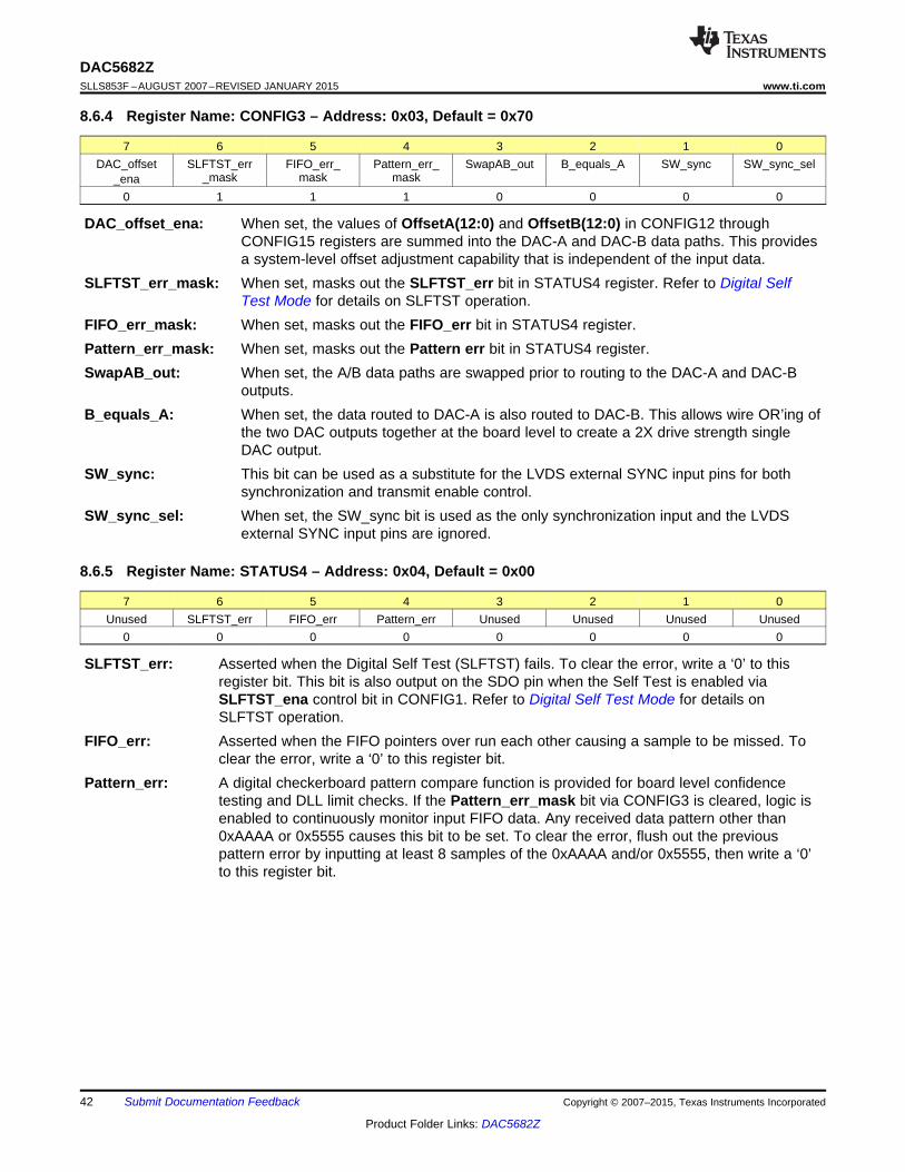
DAC5682ZSLLS853F –AUGUST 2007–REVISED JANUARY 2015 www.ti.com
8.6.4 Register Name: CONFIG3 – Address: 0x03, Default = 0x70
7 6 5 4 3 2 1 0DAC_offset SLFTST_err FIFO_err_ Pattern_err_ SwapAB_out B_equals_A SW_sync SW_sync_sel
_mask mask mask_ena0 1 1 1 0 0 0 0
DAC_offset_ena: When set, the values of OffsetA(12:0) and OffsetB(12:0) in CONFIG12 throughCONFIG15 registers are summed into the DAC-A and DAC-B data paths. This providesa system-level offset adjustment capability that is independent of the input data.
SLFTST_err_mask: When set, masks out the SLFTST_err bit in STATUS4 register. Refer to Digital SelfTest Mode for details on SLFTST operation.
FIFO_err_mask: When set, masks out the FIFO_err bit in STATUS4 register.Pattern_err_mask: When set, masks out the Pattern err bit in STATUS4 register.SwapAB_out: When set, the A/B data paths are swapped prior to routing to the DAC-A and DAC-B
outputs.B_equals_A: When set, the data routed to DAC-A is also routed to DAC-B. This allows wire OR’ing of
the two DAC outputs together at the board level to create a 2X drive strength singleDAC output.
SW_sync: This bit can be used as a substitute for the LVDS external SYNC input pins for bothsynchronization and transmit enable control.
SW_sync_sel: When set, the SW_sync bit is used as the only synchronization input and the LVDSexternal SYNC input pins are ignored.
8.6.5 Register Name: STATUS4 – Address: 0x04, Default = 0x00
7 6 5 4 3 2 1 0Unused SLFTST_err FIFO_err Pattern_err Unused Unused Unused Unused
0 0 0 0 0 0 0 0
SLFTST_err: Asserted when the Digital Self Test (SLFTST) fails. To clear the error, write a ‘0’ to thisregister bit. This bit is also output on the SDO pin when the Self Test is enabled viaSLFTST_ena control bit in CONFIG1. Refer to Digital Self Test Mode for details onSLFTST operation.
FIFO_err: Asserted when the FIFO pointers over run each other causing a sample to be missed. Toclear the error, write a ‘0’ to this register bit.
Pattern_err: A digital checkerboard pattern compare function is provided for board level confidencetesting and DLL limit checks. If the Pattern_err_mask bit via CONFIG3 is cleared, logic isenabled to continuously monitor input FIFO data. Any received data pattern other than0xAAAA or 0x5555 causes this bit to be set. To clear the error, flush out the previouspattern error by inputting at least 8 samples of the 0xAAAA and/or 0x5555, then write a ‘0’to this register bit.
42 Submit Documentation Feedback Copyright © 2007–2015, Texas Instruments Incorporated
Product Folder Links: DAC5682Z
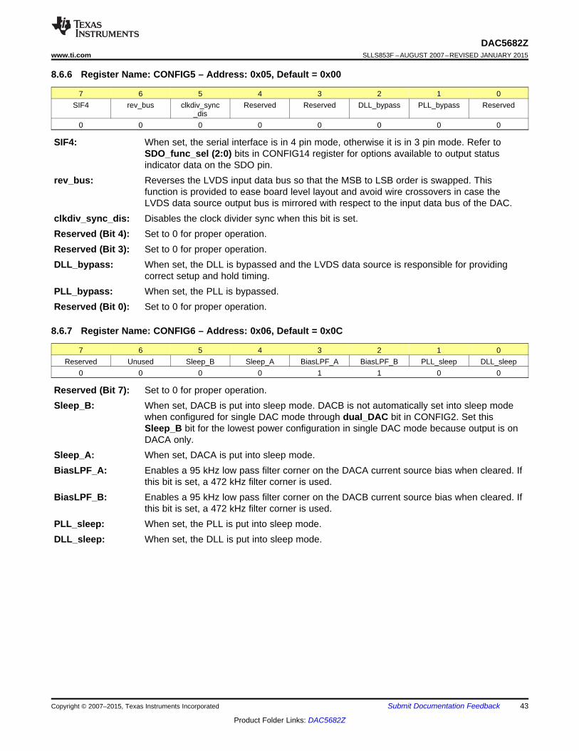
DAC5682Zwww.ti.com SLLS853F –AUGUST 2007–REVISED JANUARY 2015
8.6.6 Register Name: CONFIG5 – Address: 0x05, Default = 0x00
7 6 5 4 3 2 1 0SIF4 rev_bus clkdiv_sync Reserved Reserved DLL_bypass PLL_bypass Reserved
_dis0 0 0 0 0 0 0 0
SIF4: When set, the serial interface is in 4 pin mode, otherwise it is in 3 pin mode. Refer toSDO_func_sel (2:0) bits in CONFIG14 register for options available to output statusindicator data on the SDO pin.
rev_bus: Reverses the LVDS input data bus so that the MSB to LSB order is swapped. Thisfunction is provided to ease board level layout and avoid wire crossovers in case theLVDS data source output bus is mirrored with respect to the input data bus of the DAC.
clkdiv_sync_dis: Disables the clock divider sync when this bit is set.Reserved (Bit 4): Set to 0 for proper operation.Reserved (Bit 3): Set to 0 for proper operation.DLL_bypass: When set, the DLL is bypassed and the LVDS data source is responsible for providing
correct setup and hold timing.PLL_bypass: When set, the PLL is bypassed.Reserved (Bit 0): Set to 0 for proper operation.
8.6.7 Register Name: CONFIG6 – Address: 0x06, Default = 0x0C
7 6 5 4 3 2 1 0Reserved Unused Sleep_B Sleep_A BiasLPF_A BiasLPF_B PLL_sleep DLL_sleep
0 0 0 0 1 1 0 0
Reserved (Bit 7): Set to 0 for proper operation.Sleep_B: When set, DACB is put into sleep mode. DACB is not automatically set into sleep mode
when configured for single DAC mode through dual_DAC bit in CONFIG2. Set thisSleep_B bit for the lowest power configuration in single DAC mode because output is onDACA only.
Sleep_A: When set, DACA is put into sleep mode.BiasLPF_A: Enables a 95 kHz low pass filter corner on the DACA current source bias when cleared. If
this bit is set, a 472 kHz filter corner is used.BiasLPF_B: Enables a 95 kHz low pass filter corner on the DACB current source bias when cleared. If
this bit is set, a 472 kHz filter corner is used.PLL_sleep: When set, the PLL is put into sleep mode.DLL_sleep: When set, the DLL is put into sleep mode.
Copyright © 2007–2015, Texas Instruments Incorporated Submit Documentation Feedback 43
Product Folder Links: DAC5682Z
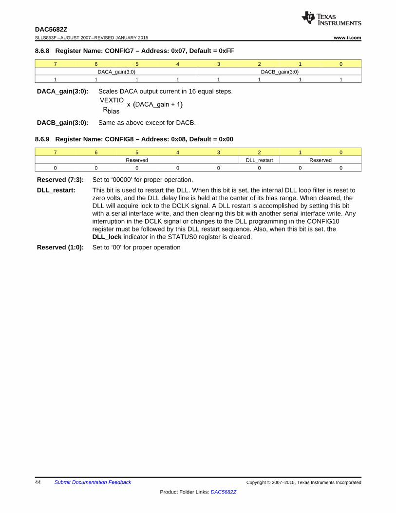
( )VEXTIO
x DACA_gain + 1Rbias
DAC5682ZSLLS853F –AUGUST 2007–REVISED JANUARY 2015 www.ti.com
8.6.8 Register Name: CONFIG7 – Address: 0x07, Default = 0xFF
7 6 5 4 3 2 1 0DACA_gain(3:0) DACB_gain(3:0)
1 1 1 1 1 1 1 1
DACA_gain(3:0): Scales DACA output current in 16 equal steps.
DACB_gain(3:0): Same as above except for DACB.
8.6.9 Register Name: CONFIG8 – Address: 0x08, Default = 0x00
7 6 5 4 3 2 1 0Reserved DLL_restart Reserved
0 0 0 0 0 0 0 0
Reserved (7:3): Set to ‘00000’ for proper operation.DLL_restart: This bit is used to restart the DLL. When this bit is set, the internal DLL loop filter is reset to
zero volts, and the DLL delay line is held at the center of its bias range. When cleared, theDLL will acquire lock to the DCLK signal. A DLL restart is accomplished by setting this bitwith a serial interface write, and then clearing this bit with another serial interface write. Anyinterruption in the DCLK signal or changes to the DLL programming in the CONFIG10register must be followed by this DLL restart sequence. Also, when this bit is set, theDLL_lock indicator in the STATUS0 register is cleared.
Reserved (1:0): Set to ‘00’ for proper operation
44 Submit Documentation Feedback Copyright © 2007–2015, Texas Instruments Incorporated
Product Folder Links: DAC5682Z
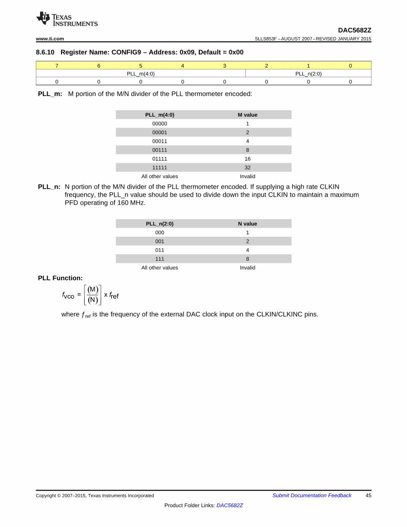
( )( )M
= xvco refN
f fé ùê úê úë û
DAC5682Zwww.ti.com SLLS853F –AUGUST 2007–REVISED JANUARY 2015
8.6.10 Register Name: CONFIG9 – Address: 0x09, Default = 0x00
7 6 5 4 3 2 1 0PLL_m(4:0) PLL_n(2:0)
0 0 0 0 0 0 0 0
PLL_m: M portion of the M/N divider of the PLL thermometer encoded:
PLL_m(4:0) M value00000 100001 200011 400111 801111 1611111 32
All other values Invalid
PLL_n: N portion of the M/N divider of the PLL thermometer encoded. If supplying a high rate CLKINfrequency, the PLL_n value should be used to divide down the input CLKIN to maintain a maximumPFD operating of 160 MHz.
PLL_n(2:0) N value000 1001 2011 4111 8
All other values Invalid
PLL Function:
where ƒref is the frequency of the external DAC clock input on the CLKIN/CLKINC pins.
Copyright © 2007–2015, Texas Instruments Incorporated Submit Documentation Feedback 45
Product Folder Links: DAC5682Z
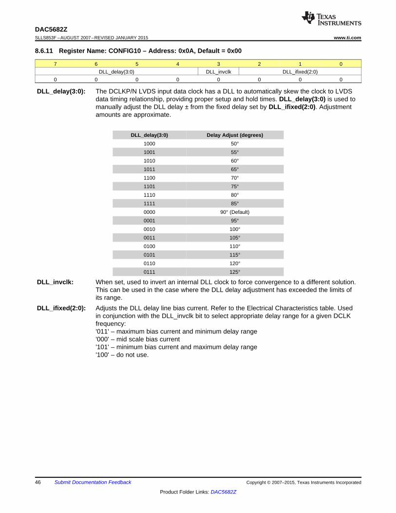
DAC5682ZSLLS853F –AUGUST 2007–REVISED JANUARY 2015 www.ti.com
8.6.11 Register Name: CONFIG10 – Address: 0x0A, Default = 0x00
7 6 5 4 3 2 1 0DLL_delay(3:0) DLL_invclk DLL_ifixed(2:0)
0 0 0 0 0 0 0 0
DLL_delay(3:0): The DCLKP/N LVDS input data clock has a DLL to automatically skew the clock to LVDSdata timing relationship, providing proper setup and hold times. DLL_delay(3:0) is used tomanually adjust the DLL delay ± from the fixed delay set by DLL_ifixed(2:0). Adjustmentamounts are approximate.
DLL_delay(3:0) Delay Adjust (degrees)1000 50°1001 55°1010 60°1011 65°1100 70°1101 75°1110 80°1111 85°0000 90° (Default)0001 95°0010 100°0011 105°0100 110°0101 115°0110 120°0111 125°
DLL_invclk: When set, used to invert an internal DLL clock to force convergence to a different solution.This can be used in the case where the DLL delay adjustment has exceeded the limits ofits range.
DLL_ifixed(2:0): Adjusts the DLL delay line bias current. Refer to the Electrical Characteristics table. Usedin conjunction with the DLL_invclk bit to select appropriate delay range for a given DCLKfrequency:'011' – maximum bias current and minimum delay range'000' – mid scale bias current'101' – minimum bias current and maximum delay range'100' – do not use.
46 Submit Documentation Feedback Copyright © 2007–2015, Texas Instruments Incorporated
Product Folder Links: DAC5682Z
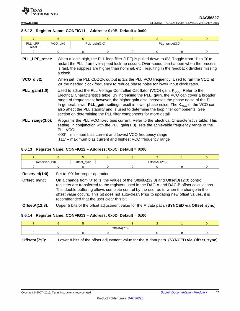
DAC5682Zwww.ti.com SLLS853F –AUGUST 2007–REVISED JANUARY 2015
8.6.12 Register Name: CONFIG11 – Address: 0x0B, Default = 0x00
7 6 5 4 3 2 1 0PLL_LPF_ VCO_div2 PLL_gain(1:0) PLL_range(3:0)
reset0 0 0 0 0 0 0 0
PLL_LPF_reset: When a logic high, the PLL loop filter (LPF) is pulled down to 0V. Toggle from ‘1’ to ‘0’ torestart the PLL if an over-speed lock-up occurs. Over-speed can happen when the processis fast, the supplies are higher than nominal, etc., resulting in the feedback dividers missinga clock.
VCO_div2: When set, the PLL CLOCK output is 1/2 the PLL VCO frequency. Used to run the VCO at2X the needed clock frequency to reduce phase noise for lower input clock rates.
PLL_gain(1:0): Used to adjust the PLL Voltage Controlled Oscillator (VCO) gain, KVCO. Refer to theElectrical Characteristics table. By increasing the PLL_gain, the VCO can cover a broaderrange of frequencies; however, the higher gain also increases the phase noise of the PLL.In general, lower PLL_gain settings result in lower phase noise. The KVCO of the VCO canalso affect the PLL stability and is used to determine the loop filter components. Seesection on determining the PLL filter components for more detail.
PLL_range(3:0): Programs the PLL VCO fixed bias current. Refer to the Electrical Characteristics table. Thissetting, in conjunction with the PLL_gain(1:0), sets the achievable frequency range of thePLL VCO:'000' – minimum bias current and lowest VCO frequency range'111' – maximum bias current and highest VCO frequency range
8.6.13 Register Name: CONFIG12 – Address: 0x0C, Default = 0x00
7 6 5 4 3 2 1 0Reserved(1:0) Offset_sync OffsetA(12:8)
0 0 0 0 0 0 0 0
Reserved(1:0): Set to ‘00’ for proper operation.Offset_sync: On a change from ‘0’ to ‘1’ the values of the OffsetA(12:0) and OffsetB(12:0) control
registers are transferred to the registers used in the DAC-A and DAC-B offset calculations.This double buffering allows complete control by the user as to when the change in theoffset value occurs. This bit does not auto-clear. Prior to updating new offset values, it isrecommended that the user clear this bit.
OffsetA(12:8): Upper 5 bits of the offset adjustment value for the A data path. (SYNCED via Offset_sync)
8.6.14 Register Name: CONFIG13 – Address: 0x0D, Default = 0x00
7 6 5 4 3 2 1 0OffsetA(7:0)
0 0 0 0 0 0 0 0
OffsetA(7:0): Lower 8 bits of the offset adjustment value for the A data path. (SYNCED via Offset_sync)
Copyright © 2007–2015, Texas Instruments Incorporated Submit Documentation Feedback 47
Product Folder Links: DAC5682Z
DAC5682ZSLLS853F –AUGUST 2007–REVISED JANUARY 2015 www.ti.com
8.6.15 Register Name: CONFIG14 – Address: 0x0E, Default = 0x00
7 6 5 4 3 2 1 0SDO_func_sel(2:0) OffsetB(12:8)
0 0 0 0 0 0 0 0
SDO_func_sel(2:0): Selects the signal for output on the SDO pin. When using the 3 pin serial interfacemode, this allows the user to multiplex several status indicators onto the SDO pin. In 4pin serial interface mode, programming this register to view one of the 5 available statusindicators will override normal SDO serial interface operation.
SDO_func_sel Output to SDO(2:0)
000, 110, 111 Normal SDO function001 PLL_lock010 DLL_lock011 Pattern_err100 FIFO_err101 SLFTST_err
OffsetB(12:8): Upper 5 bits of the offset adjustment value for the B data path. (SYNCED via Offset_sync)
8.6.16 Register Name: CONFIG15 – Address: 0x0F, Default = 0x00
7 6 5 4 3 2 1 0OffsetB(7:0)
0 0 0 0 0 0 0 0
OffsetB(7:0): Lower 8 bits of the offset adjustment value for the B data path. (SYNCED via Offset_sync)
48 Submit Documentation Feedback Copyright © 2007–2015, Texas Instruments Incorporated
Product Folder Links: DAC5682Z
DAC5682Zwww.ti.com SLLS853F –AUGUST 2007–REVISED JANUARY 2015
9 Application and Implementation
NOTEInformation in the following applications sections is not part of the TI componentspecification, and TI does not warrant its accuracy or completeness. TI’s customers areresponsible for determining suitability of components for their purposes. Customers shouldvalidate and test their design implementation to confirm system functionality.
9.1 Application InformationThe DAC5682z is a high-speed, wide bandwidth Digital-to-Analog converter. The dual DAC outputs can sampleat 1Gsps allowing synthesis of complex IQ signals from -400 to 400 MHz with a complex bandwidth of up to 400MHz. When the DAC is operated in single channel bypass mode, the maximum data rate is 1Gsps and cansustain a signal bandwidth of 500 MHz. The interpolation modes of the DAC allow the input baseband rates to be2-4 times slower than the DAC output rate reducing the processing requirements of the digital basebandprocessor and simplifies the DAC image filtering requirements. The coarse mixing blocks within the DAC allowpower efficient placement of the final carrier at the DAC output. Typically this dual DAC with its digital features isvery well equipped for complex quadrature communications applications, however it is also suitable for use inapplications that require arbitrary waveform generation.
9.2 Typical ApplicationA typical application for the DAC5682z is a wideband transmitter. The DAC is provided with some input digitalbaseband signal and it outputs an analog carrier. A typical configuration is described below.• Dual DAC mode• Datarate = 491.52 Msps (DCLK LVPECL or LVDS)• 2x Interpolation• External clock mode = 983.04 MHz (CLKIN LVPECL or LVDS)• Input data = 4C WCDMA with IF frequency at 184.32 MHz• AVDD/IOVDD = 3.3 V• DVDD/CLKVDD=1.8 V• SYNCP/N = LVDS "1"• IOUTAP/N and IOUTBP/N to transformers
Copyright © 2007–2015, Texas Instruments Incorporated Submit Documentation Feedback 49
Product Folder Links: DAC5682Z
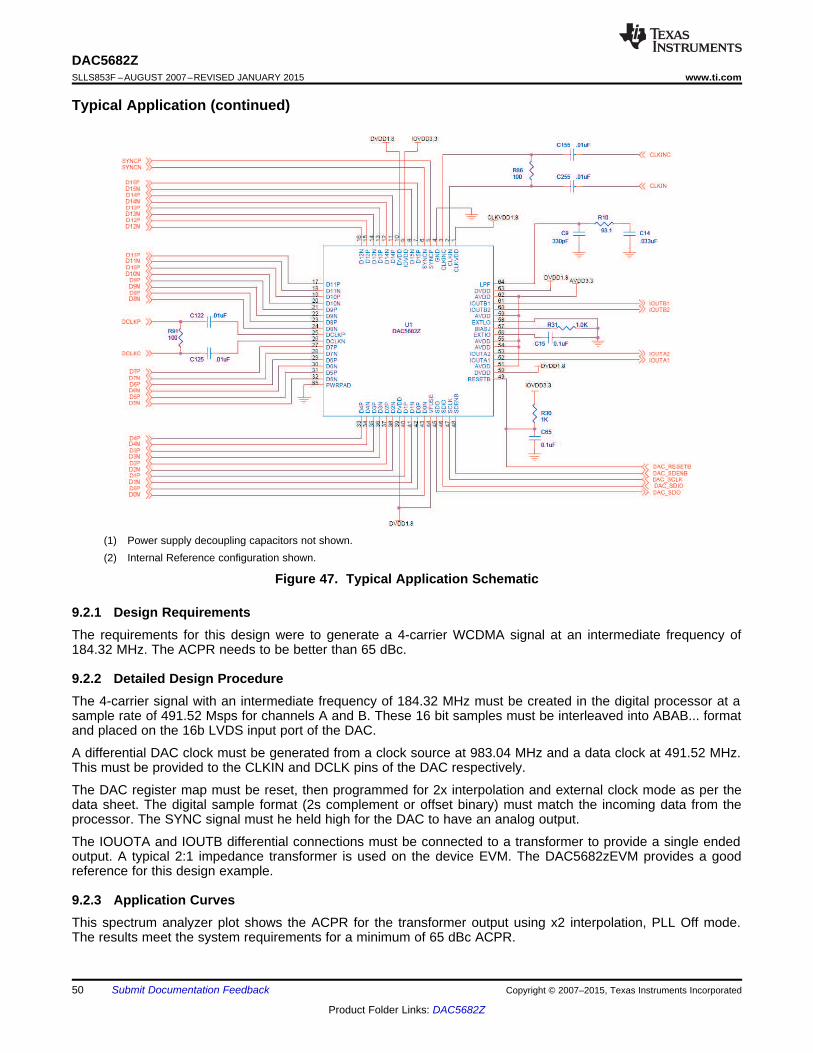
DAC5682ZSLLS853F –AUGUST 2007–REVISED JANUARY 2015 www.ti.com
Typical Application (continued)
(1) Power supply decoupling capacitors not shown.(2) Internal Reference configuration shown.
Figure 47. Typical Application Schematic
9.2.1 Design RequirementsThe requirements for this design were to generate a 4-carrier WCDMA signal at an intermediate frequency of184.32 MHz. The ACPR needs to be better than 65 dBc.
9.2.2 Detailed Design ProcedureThe 4-carrier signal with an intermediate frequency of 184.32 MHz must be created in the digital processor at asample rate of 491.52 Msps for channels A and B. These 16 bit samples must be interleaved into ABAB... formatand placed on the 16b LVDS input port of the DAC.
A differential DAC clock must be generated from a clock source at 983.04 MHz and a data clock at 491.52 MHz.This must be provided to the CLKIN and DCLK pins of the DAC respectively.
The DAC register map must be reset, then programmed for 2x interpolation and external clock mode as per thedata sheet. The digital sample format (2s complement or offset binary) must match the incoming data from theprocessor. The SYNC signal must he held high for the DAC to have an analog output.
The IOUOTA and IOUTB differential connections must be connected to a transformer to provide a single endedoutput. A typical 2:1 impedance transformer is used on the device EVM. The DAC5682zEVM provides a goodreference for this design example.
9.2.3 Application CurvesThis spectrum analyzer plot shows the ACPR for the transformer output using x2 interpolation, PLL Off mode.The results meet the system requirements for a minimum of 65 dBc ACPR.
50 Submit Documentation Feedback Copyright © 2007–2015, Texas Instruments Incorporated
Product Folder Links: DAC5682Z
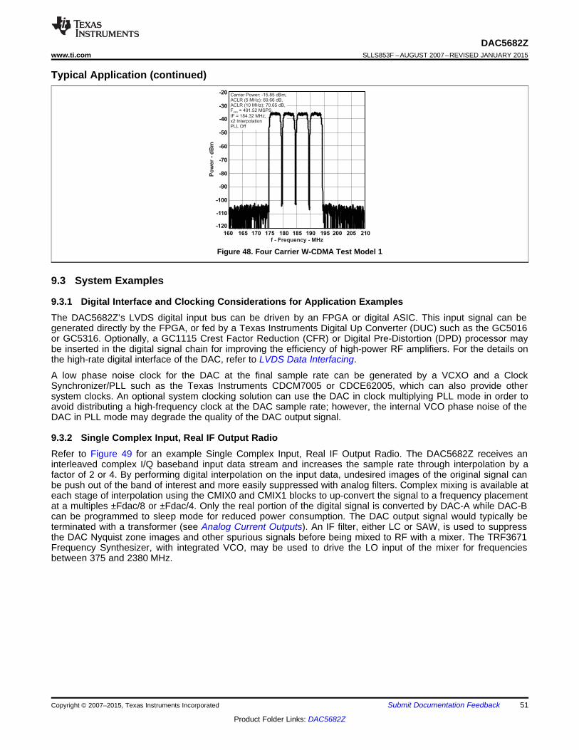
-120
-110
-100
-90
-80
-70
-60
-50
-40
-30
-20
160 165 170 175 180 185 190 195 200 205 210f - Frequency - MHz
Po
wer
- d
Bm
Carrier Power: -15.85 dBm,ACLR (5 MHz): 69.66 dB,ACLR (10 MHz): 70.65 dB,F = 491.52 MSPS,
IF = 184.32 MHz,x2 InterpolationPLL Off
data
DAC5682Zwww.ti.com SLLS853F –AUGUST 2007–REVISED JANUARY 2015
Typical Application (continued)
Figure 48. Four Carrier W-CDMA Test Model 1
9.3 System Examples
9.3.1 Digital Interface and Clocking Considerations for Application ExamplesThe DAC5682Z’s LVDS digital input bus can be driven by an FPGA or digital ASIC. This input signal can begenerated directly by the FPGA, or fed by a Texas Instruments Digital Up Converter (DUC) such as the GC5016or GC5316. Optionally, a GC1115 Crest Factor Reduction (CFR) or Digital Pre-Distortion (DPD) processor maybe inserted in the digital signal chain for improving the efficiency of high-power RF amplifiers. For the details onthe high-rate digital interface of the DAC, refer to LVDS Data Interfacing.
A low phase noise clock for the DAC at the final sample rate can be generated by a VCXO and a ClockSynchronizer/PLL such as the Texas Instruments CDCM7005 or CDCE62005, which can also provide othersystem clocks. An optional system clocking solution can use the DAC in clock multiplying PLL mode in order toavoid distributing a high-frequency clock at the DAC sample rate; however, the internal VCO phase noise of theDAC in PLL mode may degrade the quality of the DAC output signal.
9.3.2 Single Complex Input, Real IF Output RadioRefer to Figure 49 for an example Single Complex Input, Real IF Output Radio. The DAC5682Z receives aninterleaved complex I/Q baseband input data stream and increases the sample rate through interpolation by afactor of 2 or 4. By performing digital interpolation on the input data, undesired images of the original signal canbe push out of the band of interest and more easily suppressed with analog filters. Complex mixing is available ateach stage of interpolation using the CMIX0 and CMIX1 blocks to up-convert the signal to a frequency placementat a multiples ±Fdac/8 or ±Fdac/4. Only the real portion of the digital signal is converted by DAC-A while DAC-Bcan be programmed to sleep mode for reduced power consumption. The DAC output signal would typically beterminated with a transformer (see Analog Current Outputs). An IF filter, either LC or SAW, is used to suppressthe DAC Nyquist zone images and other spurious signals before being mixed to RF with a mixer. The TRF3671Frequency Synthesizer, with integrated VCO, may be used to drive the LO input of the mixer for frequenciesbetween 375 and 2380 MHz.
Copyright © 2007–2015, Texas Instruments Incorporated Submit Documentation Feedback 51
Product Folder Links: DAC5682Z
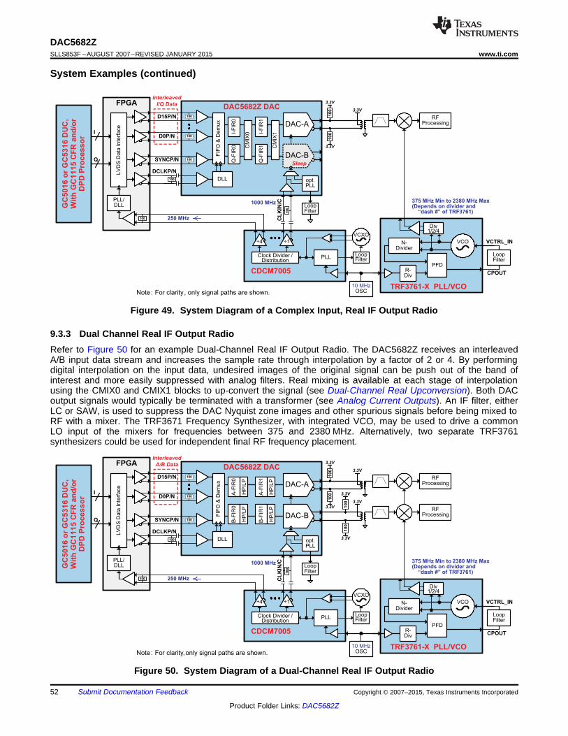
DAC-A
DAC-B
B-F
IR1
HP
/LP
A-F
IR1
HP
/LP
B-F
IR0
A-F
IR0
FIF
O&
Dem
ux
100
100
100
100
CL
KIN
/C
opt.PLL
LoopFilter
DLL
DAC5682Z DAC
10
0
FPGA
PLL
÷1÷4
Clock Divider /Distribution
CDCM7005
100 250 MHz
1000 MHzPLL/DLL
VCON-Divider
R-Div
PFD
CPOUT
VCTRL_IN
TRF3761-X PLL/VCO
LoopFilter
Div1/2/4
DCLKP/N
SYNCP/N
D0P/N
D15P/N
375 MHz Min to 2380 MHz Max(Depends on divider and
“dash #” of TRF3761)
10 MHzOSCNote: For clarity,only signal paths are shown.
LV
DS
Data
Inte
rface
LoopFilter
VCXO
I
Q
GC
50
16
or
GC
53
16
DU
C,
Wit
hG
C1
11
5C
FR
an
d/o
rD
PD
Pro
ce
ss
or
3.3V
100 3.3V
3.3V
3.3V
100 3.3V
100
3.3V
100
RFProcessing
RFProcessing
Interleaved
A/B Data
HP
/LP
HP
/LP
DAC-A
DAC-B
Q-F
IR1 C
MIX
1I-F
IR1
CM
IX0
Q-F
IR0
I-F
IR0
FIF
O&
Dem
ux
100
100
100
100
CL
KIN
/C
opt.PLL
LoopFilter
DLL
DAC5682Z DAC
10
0
FPGA
PLL
÷1÷4
Clock Divider /Distribution
CDCM7005
100 250 MHz
1000 MHzPLL/DLL
VCON-Divider
R-Div
PFD
CPOUT
VCTRL_IN
TRF3761-X PLL/VCO
LoopFilter
Div1/2/4
DCLKP/N
SYNCP/N
D0P/N
D15P/N
375 MHz Min to 2380 MHz Max(Depends on divider and
“dash #” of TRF3761)
10 MHzOSCNote: For clarity, only signal paths are shown.
LV
DS
Data
Inte
rface
LoopFilter
VCXO
I
Q
GC
50
16
or
GC
53
16
DU
C,
Wit
hG
C1
11
5C
FR
an
d/o
rD
PD
Pro
ce
ss
or
3.3V
100 3.3V
3.3V
100
RFProcessing
Interleaved
I/Q Data
Sleep
DAC5682ZSLLS853F –AUGUST 2007–REVISED JANUARY 2015 www.ti.com
System Examples (continued)
Figure 49. System Diagram of a Complex Input, Real IF Output Radio
9.3.3 Dual Channel Real IF Output RadioRefer to Figure 50 for an example Dual-Channel Real IF Output Radio. The DAC5682Z receives an interleavedA/B input data stream and increases the sample rate through interpolation by a factor of 2 or 4. By performingdigital interpolation on the input data, undesired images of the original signal can be push out of the band ofinterest and more easily suppressed with analog filters. Real mixing is available at each stage of interpolationusing the CMIX0 and CMIX1 blocks to up-convert the signal (see Dual-Channel Real Upconversion). Both DACoutput signals would typically be terminated with a transformer (see Analog Current Outputs). An IF filter, eitherLC or SAW, is used to suppress the DAC Nyquist zone images and other spurious signals before being mixed toRF with a mixer. The TRF3671 Frequency Synthesizer, with integrated VCO, may be used to drive a commonLO input of the mixers for frequencies between 375 and 2380 MHz. Alternatively, two separate TRF3761synthesizers could be used for independent final RF frequency placement.
Figure 50. System Diagram of a Dual-Channel Real IF Output Radio
52 Submit Documentation Feedback Copyright © 2007–2015, Texas Instruments Incorporated
Product Folder Links: DAC5682Z
DAC5682Zwww.ti.com SLLS853F –AUGUST 2007–REVISED JANUARY 2015
System Examples (continued)9.3.4 Direct Conversion RadioRefer to Figure 51 for an example Direct Conversion Radio. The DAC5682Z receives an interleaved complex I/Qbaseband input data stream and increases the sample rate through interpolation by a factor of 2 or 4. Byperforming digital interpolation on the input data, undesired images of the original signal can be push out of theband of interest and more easily suppressed with analog filters.
For a Zero IF (ZIF) frequency plan, complex mixing of the baseband signal is not required. Alternatively, for aComplex IF frequency plan the input data can be placed at an pre-placed at an IF within the bandwidthlimitations of the interpolation filters. In addition, complex mixing is available at each stage of interpolation usingthe CMIX0 and CMIX1 blocks to up-convert the signal to a frequency placement at a multiples ±Fdac/8 or±Fdac/4. The output of both DAC channels is used to produce a Hilbert transform pair and can be expressed as:
A(t) = I(t)cos(ωct) – Q(t)sin(ωct) m(t) (14)A(t) = I(t)cos(ωct) – Q(t)sin(ωct) mh(t) (15)
where m(t) and mh(t) connote a Hilbert transform pair and ωc is the sum of the CMIX0 and CMIX1 frequencies.The complex output is input to an analog quadrature modulator (AQM) such as the Texas Instruments TRF3703-33 for a single side-band (SSB) up conversion to RF. A passive (resistor only) interface to the AQM isrecommended, with an optional LC filter network. The TRF3671 Frequency Synthesizer with integrated VCO maybe used to drive the LO input of the TRF3703-33 for frequencies between 375 and 2380 MHz. Upper single-sideband upconversion is achieved at the output of the analog quadrature modulator, whose output is expressedas:
RF(t) = I(t)cos(ωc + ωLO)t – Q(t)sin(ωc + ωLO)t (16)
Flexibility is provided to the user by allowing for the selection of negative CMIX mixing sequences to produce alower-sideband upconversion. Note that the process of complex mixing translates the signal frequency from 0 Hzmeans that the analog quadrature modulator IQ imbalance produces a sideband that falls outside the signal ofinterest. DC offset error in DAC and AQM signal path may produce LO feed-through at the RF output which mayfall in the band of interest. To suppress the LO feed-through, the DAC5682Z provides a digital offset correctioncapability for both DAC-A and DAC-B paths. (See DAC_offset_ena bit in CONFIG3.)
The complex IF architecture has several advantages over the real IF architecture:• Uncalibrated side-band suppression ~ 35 dBc compared to 0 dBc for real IF architecture.• Direct DAC to AQM interface – no amplifiers required• Nonharmonic clock-related spurious signals fall out-of-band• DAC 2nd Nyquist zone image is offset fDAC compared with fDAC– 2 × IF for a real IF architecture, reducing the
need for filtering at the DAC output.• Uncalibrated LO feed through for AQM is ~ 35 dBc and calibration can reduce or completely remove the LO
feed through.
Copyright © 2007–2015, Texas Instruments Incorporated Submit Documentation Feedback 53
Product Folder Links: DAC5682Z
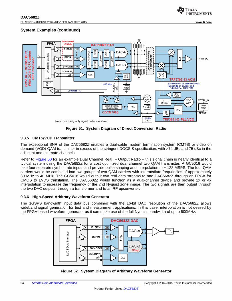
DAC-A
DAC-B
FIF
O
100
100
100
100 DLL
DAC5682Z DACFPGA
DCLKP/N
SYNCP/N
D0P/N
D15P/N
LV
DS
Data
Inte
rface
Sleep
DAC-A
DAC-B
Q-F
IR1 C
MIX
1I-F
IR1
CM
IX0
Q-F
IR0
I-F
IR0
FIF
O&
Dem
ux
100
100
100
CL
KIN
/C
opt.PLL
LoopFilter
DLL
DAC5682Z DAC
10
0
FPGA
PLL
÷1÷4
Clock Divider /Distribution
CDCM7005
100 250 MHz
1000 MHzPLL/DLL
VCON-Divider
R-Div
PFD
CPOUT
VCTRL_IN
900
TRF3703-33 AQM
TRF3761-X PLL/VCO
LoopFilter
Div1/2/4
375 MHz Min to 2380 MHz Max(Depends on divider and
“dash #” of TRF3761)
10 MHzOSC
RF OUT
Note: For clarity,only signal paths are shown .
Op
tio
nal
(100
oh
m)
Filte
rN
etw
ork
LV
DS
Data
Inte
rface
LoopFilter
VCXO
I
Q
GC
50
16
or
GC
53
16
DU
C,
Wit
hG
C1
15
CF
Ra
nd
/or
DP
DP
roc
es
so
r
5V
115
634
115
634
115
115
634
634
100
DCLKP/N
SYNCP/N
D0P/N
D15P/N
Interleaved
I/Q Data
DAC5682ZSLLS853F –AUGUST 2007–REVISED JANUARY 2015 www.ti.com
System Examples (continued)
Figure 51. System Diagram of Direct Conversion Radio
9.3.5 CMTS/VOD TransmitterThe exceptional SNR of the DAC5682Z enables a dual-cable modem termination system (CMTS) or video ondemand (VOD) QAM transmitter in excess of the stringent DOCSIS specification, with >74 dBc and 75 dBc in theadjacent and alternate channels.
Refer to Figure 50 for an example Dual Channel Real IF Output Radio – this signal chain is nearly identical to atypical system using the DAC5682Z for a cost optimized dual channel two QAM transmitter. A GC5016 wouldtake four separate symbol rate inputs and provide pulse shaping and interpolation to ~ 128 MSPS. The four QAMcarriers would be combined into two groups of two QAM carriers with intermediate frequencies of approximately30 MHz to 40 MHz. The GC5016 would output two real data streams to one DAC5682Z through an FPGA forCMOS to LVDS translation. The DAC5682Z would function as a dual-channel device and provide 2x or 4xinterpolation to increase the frequency of the 2nd Nyquist zone image. The two signals are then output throughthe two DAC outputs, through a transformer and to an RF upconverter.
9.3.6 High-Speed Arbitrary Waveform GeneratorThe 1GSPS bandwidth input data bus combined with the 16-bit DAC resolution of the DAC5682Z allowswideband signal generation for test and measurement applications. In this case, interpolation is not desired bythe FPGA-based waveform generator as it can make use of the full Nyquist bandwidth of up to 500MHz.
Figure 52. System Diagram of Arbitrary Waveform Generator
54 Submit Documentation Feedback Copyright © 2007–2015, Texas Instruments Incorporated
Product Folder Links: DAC5682Z
DAC5682Zwww.ti.com SLLS853F –AUGUST 2007–REVISED JANUARY 2015
9.4 Initialization Set Up
9.4.1 Recommended Start-up SequenceThe following start-up sequence is recommended to initialize the DAC5682Z:1. Supply all 1.8 V (CLKVDD, DVDD, VFUSE) voltages simultaneously followed by all 3.3 V (AVDD and
IOVDD) voltages.2. Provide stable CLKIN/C clock.3. Toggle RESETB pin for a minimum 25 nSec active low pulse width.4. Program all desired SIF registers. Set DLL_Restart bit during this write cycle. The CONFIG10 register value
should match the corresponding DCLKP/N frequency range in the Electrical Characteristics table.5. Provide stable DCLKP/N clock. (This can also be provided earlier in the sequence)6. Clear the DLL_Restart bit when the DCLKP/N clock is expected to be stable.7. Verify the status of DLL_Lock and repeat until set to ‘1’. DLL_Lock can be monitored by reading the
STATUS0 register or by monitoring the SDO pin in 3-wire SIF mode. (See description for CONFIG14SDO_func_sel.)
8. Enable transmit of data by asserting the LVDS SYNCP/N input or setting CONFIG3 SW_sync bit. (Seedescription for CONFIG3 SW_sync and SW_sync_sel) The SYNC source must be held at a logic ‘1’ toenable data flow through the DAC. If multiple DAC devices require synchronization, refer to the"Recommended Multi-DAC Synchronization Procedure" below.
9. Provide data flow to LVDS D[15:0]P/N pins. If using the LVDS SYNCP/N input, data can be inputsimultaneous with the logic ‘1’ transition of SYNCP/N.
10 Power Supply RecommendationsIt is recommended that the device be powered with the nominal supply voltages as indicated in theRecommended Operating Conditions.
In most instances the best performance is achieved with LDO supplies. However the supplies may be driven withdirect outputs from a DC-DC switcher as long as the noise performance of the switcher is acceptable.
For an LDO power supply reference, it is best to refer to the DAC5682zEVM.
Copyright © 2007–2015, Texas Instruments Incorporated Submit Documentation Feedback 55
Product Folder Links: DAC5682Z
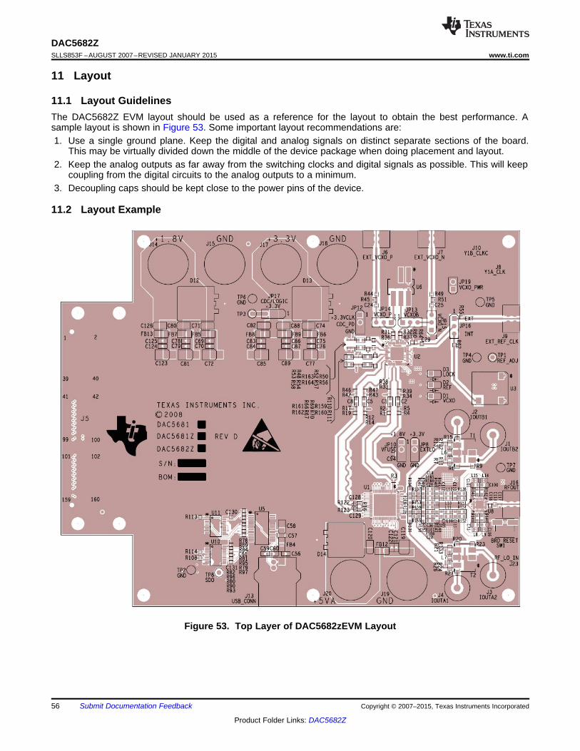
DAC5682ZSLLS853F –AUGUST 2007–REVISED JANUARY 2015 www.ti.com
11 Layout
11.1 Layout GuidelinesThe DAC5682Z EVM layout should be used as a reference for the layout to obtain the best performance. Asample layout is shown in Figure 53. Some important layout recommendations are:1. Use a single ground plane. Keep the digital and analog signals on distinct separate sections of the board.
This may be virtually divided down the middle of the device package when doing placement and layout.2. Keep the analog outputs as far away from the switching clocks and digital signals as possible. This will keep
coupling from the digital circuits to the analog outputs to a minimum.3. Decoupling caps should be kept close to the power pins of the device.
11.2 Layout Example
Figure 53. Top Layer of DAC5682zEVM Layout
56 Submit Documentation Feedback Copyright © 2007–2015, Texas Instruments Incorporated
Product Folder Links: DAC5682Z
DAC5682Zwww.ti.com SLLS853F –AUGUST 2007–REVISED JANUARY 2015
12 Device and Documentation Support
12.1 Device Support
12.1.1 Third-Party Products DisclaimerTI'S PUBLICATION OF INFORMATION REGARDING THIRD-PARTY PRODUCTS OR SERVICES DOES NOTCONSTITUTE AN ENDORSEMENT REGARDING THE SUITABILITY OF SUCH PRODUCTS OR SERVICESOR A WARRANTY, REPRESENTATION OR ENDORSEMENT OF SUCH PRODUCTS OR SERVICES, EITHERALONE OR IN COMBINATION WITH ANY TI PRODUCT OR SERVICE.
12.1.2 Device NomenclatureAdjacent Carrier Leakage Ratio (ACLR): Defined for a 3.84Mcps 3GPP W-CDMA input signal measured in a3.84MHz bandwidth at a 5MHz offset from the carrier with a 12dB peak-to-average ratio.
Analog and Digital Power Supply Rejection Ratio (APSSR, DPSSR): Defined as the percentage error in theratio of the delta IOUT and delta supply voltage normalized with respect to the ideal IOUT current.
Differential Nonlinearity (DNL): Defined as the variation in analog output associated with an ideal 1 LSBchange in the digital input code.
Gain Drift: Defined as the maximum change in gain, in terms of ppm of full-scale range (FSR) per °C, from thevalue at ambient (25°C) to values over the full operating temperature range.
Gain Error: Defined as the percentage error (in FSR%) for the ratio between the measured full-scale outputcurrent and the ideal full-scale output current.
Integral Nonlinearity (INL): Defined as the maximum deviation of the actual analog output from the ideal output,determined by a straight line drawn from zero scale to full scale.
Intermodulation Distortion (IMD3, IMD): The two-tone IMD3 or four-tone IMD is defined as the ratio (in dBc) ofthe worst 3rd-order (or higher) intermodulation distortion product to either fundamental output tone.
Offset Drift: Defined as the maximum change in DC offset, in terms of ppm of full-scale range (FSR) per °C,from the value at ambient (25°C) to values over the full operating temperature range.
Offset Error: Defined as the percentage error (in FSR%) for the ratio of the differential output current(IOUT1–IOUT2) and the mid-scale output current.
Output Compliance Range: Defined as the minimum and maximum allowable voltage at the output of thecurrent-output DAC. Exceeding this limit may result reduced reliability of the device or adversely affectingdistortion performance.
Reference Voltage Drift: Defined as the maximum change of the reference voltage in ppm per degree Celsiusfrom value at ambient (25°C) to values over the full operating temperature range.
Spurious Free Dynamic Range (SFDR): Defined as the difference (in dBc) between the peak amplitude of theoutput signal and the peak spurious signal.
Signal to Noise Ratio (SNR): Defined as the ratio of the RMS value of the fundamental output signal to theRMS sum of all other spectral components below the Nyquist frequency, including noise, but excluding the firstsix harmonics and dc.
12.2 TrademarksAll trademarks are the property of their respective owners.
12.3 Electrostatic Discharge CautionThese devices have limited built-in ESD protection. The leads should be shorted together or the device placed in conductive foamduring storage or handling to prevent electrostatic damage to the MOS gates.
Copyright © 2007–2015, Texas Instruments Incorporated Submit Documentation Feedback 57
Product Folder Links: DAC5682Z
DAC5682ZSLLS853F –AUGUST 2007–REVISED JANUARY 2015 www.ti.com
12.4 GlossarySLYZ022 — TI Glossary.
This glossary lists and explains terms, acronyms, and definitions.
13 Mechanical, Packaging, and Orderable InformationThe following pages include mechanical, packaging, and orderable information. This information is the mostcurrent data available for the designated devices. This data is subject to change without notice and revision ofthis document. For browser-based versions of this data sheet, refer to the left-hand navigation.
58 Submit Documentation Feedback Copyright © 2007–2015, Texas Instruments Incorporated
Product Folder Links: DAC5682Z
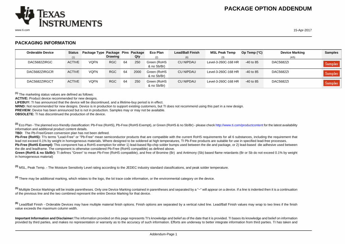
PACKAGE OPTION ADDENDUM
www.ti.com 15-Apr-2017
Addendum-Page 1
PACKAGING INFORMATION
Orderable Device Status(1)
Package Type PackageDrawing
Pins PackageQty
Eco Plan(2)
Lead/Ball Finish(6)
MSL Peak Temp(3)
Op Temp (°C) Device Marking(4/5)
Samples
DAC5682ZIRGC ACTIVE VQFN RGC 64 250 Green (RoHS& no Sb/Br)
CU NIPDAU Level-3-260C-168 HR -40 to 85 DAC5682ZI
DAC5682ZIRGCR ACTIVE VQFN RGC 64 2000 Green (RoHS& no Sb/Br)
CU NIPDAU Level-3-260C-168 HR -40 to 85 DAC5682ZI
DAC5682ZIRGCT ACTIVE VQFN RGC 64 250 Green (RoHS& no Sb/Br)
CU NIPDAU Level-3-260C-168 HR -40 to 85 DAC5682ZI
(1) The marketing status values are defined as follows:ACTIVE: Product device recommended for new designs.LIFEBUY: TI has announced that the device will be discontinued, and a lifetime-buy period is in effect.NRND: Not recommended for new designs. Device is in production to support existing customers, but TI does not recommend using this part in a new design.PREVIEW: Device has been announced but is not in production. Samples may or may not be available.OBSOLETE: TI has discontinued the production of the device.
(2) Eco Plan - The planned eco-friendly classification: Pb-Free (RoHS), Pb-Free (RoHS Exempt), or Green (RoHS & no Sb/Br) - please check http://www.ti.com/productcontent for the latest availabilityinformation and additional product content details.TBD: The Pb-Free/Green conversion plan has not been defined.Pb-Free (RoHS): TI's terms "Lead-Free" or "Pb-Free" mean semiconductor products that are compatible with the current RoHS requirements for all 6 substances, including the requirement thatlead not exceed 0.1% by weight in homogeneous materials. Where designed to be soldered at high temperatures, TI Pb-Free products are suitable for use in specified lead-free processes.Pb-Free (RoHS Exempt): This component has a RoHS exemption for either 1) lead-based flip-chip solder bumps used between the die and package, or 2) lead-based die adhesive used betweenthe die and leadframe. The component is otherwise considered Pb-Free (RoHS compatible) as defined above.Green (RoHS & no Sb/Br): TI defines "Green" to mean Pb-Free (RoHS compatible), and free of Bromine (Br) and Antimony (Sb) based flame retardants (Br or Sb do not exceed 0.1% by weightin homogeneous material)
(3) MSL, Peak Temp. - The Moisture Sensitivity Level rating according to the JEDEC industry standard classifications, and peak solder temperature.
(4) There may be additional marking, which relates to the logo, the lot trace code information, or the environmental category on the device.
(5) Multiple Device Markings will be inside parentheses. Only one Device Marking contained in parentheses and separated by a "~" will appear on a device. If a line is indented then it is a continuationof the previous line and the two combined represent the entire Device Marking for that device.
(6) Lead/Ball Finish - Orderable Devices may have multiple material finish options. Finish options are separated by a vertical ruled line. Lead/Ball Finish values may wrap to two lines if the finishvalue exceeds the maximum column width.
Important Information and Disclaimer:The information provided on this page represents TI's knowledge and belief as of the date that it is provided. TI bases its knowledge and belief on informationprovided by third parties, and makes no representation or warranty as to the accuracy of such information. Efforts are underway to better integrate information from third parties. TI has taken and
PACKAGE OPTION ADDENDUM
www.ti.com 15-Apr-2017
Addendum-Page 2
continues to take reasonable steps to provide representative and accurate information but may not have conducted destructive testing or chemical analysis on incoming materials and chemicals.TI and TI suppliers consider certain information to be proprietary, and thus CAS numbers and other limited information may not be available for release.
In no event shall TI's liability arising out of such information exceed the total purchase price of the TI part(s) at issue in this document sold by TI to Customer on an annual basis.
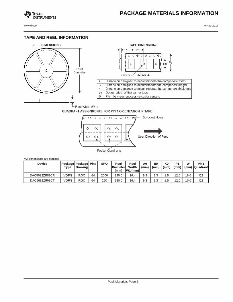
TAPE AND REEL INFORMATION
*All dimensions are nominal
Device PackageType
PackageDrawing
Pins SPQ ReelDiameter
(mm)
ReelWidth
W1 (mm)
A0(mm)
B0(mm)
K0(mm)
P1(mm)
W(mm)
Pin1Quadrant
DAC5682ZIRGCR VQFN RGC 64 2000 330.0 16.4 9.3 9.3 1.5 12.0 16.0 Q2
DAC5682ZIRGCT VQFN RGC 64 250 330.0 16.4 9.3 9.3 1.5 12.0 16.0 Q2
PACKAGE MATERIALS INFORMATION
www.ti.com 9-Aug-2017
Pack Materials-Page 1
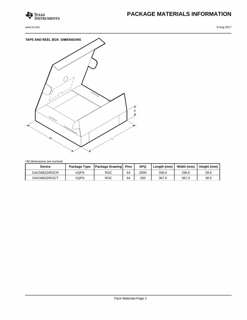
*All dimensions are nominal
Device Package Type Package Drawing Pins SPQ Length (mm) Width (mm) Height (mm)
DAC5682ZIRGCR VQFN RGC 64 2000 336.6 336.6 28.6
DAC5682ZIRGCT VQFN RGC 64 250 367.0 367.0 38.0
PACKAGE MATERIALS INFORMATION
www.ti.com 9-Aug-2017
Pack Materials-Page 2
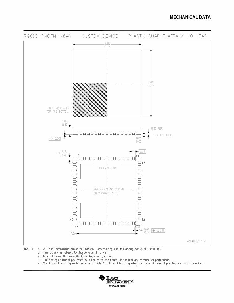
IMPORTANT NOTICE
Texas Instruments Incorporated (TI) reserves the right to make corrections, enhancements, improvements and other changes to itssemiconductor products and services per JESD46, latest issue, and to discontinue any product or service per JESD48, latest issue. Buyersshould obtain the latest relevant information before placing orders and should verify that such information is current and complete.TI’s published terms of sale for semiconductor products (http://www.ti.com/sc/docs/stdterms.htm) apply to the sale of packaged integratedcircuit products that TI has qualified and released to market. Additional terms may apply to the use or sale of other types of TI products andservices.Reproduction of significant portions of TI information in TI data sheets is permissible only if reproduction is without alteration and isaccompanied by all associated warranties, conditions, limitations, and notices. TI is not responsible or liable for such reproduceddocumentation. Information of third parties may be subject to additional restrictions. Resale of TI products or services with statementsdifferent from or beyond the parameters stated by TI for that product or service voids all express and any implied warranties for theassociated TI product or service and is an unfair and deceptive business practice. TI is not responsible or liable for any such statements.Buyers and others who are developing systems that incorporate TI products (collectively, “Designers”) understand and agree that Designersremain responsible for using their independent analysis, evaluation and judgment in designing their applications and that Designers havefull and exclusive responsibility to assure the safety of Designers' applications and compliance of their applications (and of all TI productsused in or for Designers’ applications) with all applicable regulations, laws and other applicable requirements. Designer represents that, withrespect to their applications, Designer has all the necessary expertise to create and implement safeguards that (1) anticipate dangerousconsequences of failures, (2) monitor failures and their consequences, and (3) lessen the likelihood of failures that might cause harm andtake appropriate actions. Designer agrees that prior to using or distributing any applications that include TI products, Designer willthoroughly test such applications and the functionality of such TI products as used in such applications.TI’s provision of technical, application or other design advice, quality characterization, reliability data or other services or information,including, but not limited to, reference designs and materials relating to evaluation modules, (collectively, “TI Resources”) are intended toassist designers who are developing applications that incorporate TI products; by downloading, accessing or using TI Resources in anyway, Designer (individually or, if Designer is acting on behalf of a company, Designer’s company) agrees to use any particular TI Resourcesolely for this purpose and subject to the terms of this Notice.TI’s provision of TI Resources does not expand or otherwise alter TI’s applicable published warranties or warranty disclaimers for TIproducts, and no additional obligations or liabilities arise from TI providing such TI Resources. TI reserves the right to make corrections,enhancements, improvements and other changes to its TI Resources. TI has not conducted any testing other than that specificallydescribed in the published documentation for a particular TI Resource.Designer is authorized to use, copy and modify any individual TI Resource only in connection with the development of applications thatinclude the TI product(s) identified in such TI Resource. NO OTHER LICENSE, EXPRESS OR IMPLIED, BY ESTOPPEL OR OTHERWISETO ANY OTHER TI INTELLECTUAL PROPERTY RIGHT, AND NO LICENSE TO ANY TECHNOLOGY OR INTELLECTUAL PROPERTYRIGHT OF TI OR ANY THIRD PARTY IS GRANTED HEREIN, including but not limited to any patent right, copyright, mask work right, orother intellectual property right relating to any combination, machine, or process in which TI products or services are used. Informationregarding or referencing third-party products or services does not constitute a license to use such products or services, or a warranty orendorsement thereof. Use of TI Resources may require a license from a third party under the patents or other intellectual property of thethird party, or a license from TI under the patents or other intellectual property of TI.TI RESOURCES ARE PROVIDED “AS IS” AND WITH ALL FAULTS. TI DISCLAIMS ALL OTHER WARRANTIES ORREPRESENTATIONS, EXPRESS OR IMPLIED, REGARDING RESOURCES OR USE THEREOF, INCLUDING BUT NOT LIMITED TOACCURACY OR COMPLETENESS, TITLE, ANY EPIDEMIC FAILURE WARRANTY AND ANY IMPLIED WARRANTIES OFMERCHANTABILITY, FITNESS FOR A PARTICULAR PURPOSE, AND NON-INFRINGEMENT OF ANY THIRD PARTY INTELLECTUALPROPERTY RIGHTS. TI SHALL NOT BE LIABLE FOR AND SHALL NOT DEFEND OR INDEMNIFY DESIGNER AGAINST ANY CLAIM,INCLUDING BUT NOT LIMITED TO ANY INFRINGEMENT CLAIM THAT RELATES TO OR IS BASED ON ANY COMBINATION OFPRODUCTS EVEN IF DESCRIBED IN TI RESOURCES OR OTHERWISE. IN NO EVENT SHALL TI BE LIABLE FOR ANY ACTUAL,DIRECT, SPECIAL, COLLATERAL, INDIRECT, PUNITIVE, INCIDENTAL, CONSEQUENTIAL OR EXEMPLARY DAMAGES INCONNECTION WITH OR ARISING OUT OF TI RESOURCES OR USE THEREOF, AND REGARDLESS OF WHETHER TI HAS BEENADVISED OF THE POSSIBILITY OF SUCH DAMAGES.Unless TI has explicitly designated an individual product as meeting the requirements of a particular industry standard (e.g., ISO/TS 16949and ISO 26262), TI is not responsible for any failure to meet such industry standard requirements.Where TI specifically promotes products as facilitating functional safety or as compliant with industry functional safety standards, suchproducts are intended to help enable customers to design and create their own applications that meet applicable functional safety standardsand requirements. Using products in an application does not by itself establish any safety features in the application. Designers mustensure compliance with safety-related requirements and standards applicable to their applications. Designer may not use any TI products inlife-critical medical equipment unless authorized officers of the parties have executed a special contract specifically governing such use.Life-critical medical equipment is medical equipment where failure of such equipment would cause serious bodily injury or death (e.g., lifesupport, pacemakers, defibrillators, heart pumps, neurostimulators, and implantables). Such equipment includes, without limitation, allmedical devices identified by the U.S. Food and Drug Administration as Class III devices and equivalent classifications outside the U.S.TI may expressly designate certain products as completing a particular qualification (e.g., Q100, Military Grade, or Enhanced Product).Designers agree that it has the necessary expertise to select the product with the appropriate qualification designation for their applicationsand that proper product selection is at Designers’ own risk. Designers are solely responsible for compliance with all legal and regulatoryrequirements in connection with such selection.Designer will fully indemnify TI and its representatives against any damages, costs, losses, and/or liabilities arising out of Designer’s non-compliance with the terms and provisions of this Notice.
Mailing Address: Texas Instruments, Post Office Box 655303, Dallas, Texas 75265Copyright © 2017, Texas Instruments Incorporated