Embed Size (px)
Citation preview
Procedia Engineering 15 (2011) 2388 – 2392
1877-7058 © 2011 Published by Elsevier Ltd.doi:10.1016/j.proeng.2011.08.448
Available online at www.sciencedirect.comAvailable online at www.sciencedirect.com
Procedia Engineering 00 (2011) 000–000
ProcediaEngineering
www.elsevier.com/locate/procedia
Advanced in Control Engineering and Information Science
Data Transmission Technology of Line Acquisition Unit in Seismic Acquisition System
Yinge Konga, Ming Denga, Jian Guob,Weibing Luob a* a School of Geophysics and Information Technology, China University of Geosciences in Beijing, BeiJing 100083,China
bInstitute of Geology and Geophysics,Chinese Academy of Sciences, Beijing, Beijing 100029, China
Abstract
Seismic acquisition system is the seismic prospecting equipment used for field data acquisition, usually consisting of field digitizer unit (FDU), digital sensor unit (DSU), line acquisition unit (LAU), cables and connectors etc [1]. The functions of LAU include off/on controlling and data packaging & switching etc. The combination of field programmable gate array (FPGA) and KSZ8041NL is adopted in LAU for data transmission in physical layer. The paper presents the hardware structure and relevant schematic design on program of the high rate data transmission part of LAU in seismic acquisition system. Keywords: seismic prospecting; FPGA; line acquisition unit; KSZ8041NL; data transmission;
1. Introduction
In seismic acquisition system, LAU acts as cache and transmitter of mass data and completes field seismic data acquisition with high efficiency and quality. Low power consumption and low error rate is especially important for high rate data transmission of LAUs. The paper presents a type of circuit structure based on field programmable gate array (FPGA) and KSZ8041NL for data transmission between LAUs, which makes good use of the advantage of parallel operation of FPGA and the ability to transmit data in high rate of KSZ8041NL. It can meet the requirement on rate and quality of data transmission between LAUs. The LAUs in this seismic acquisition system are able to operate at a data rate of 100Mbps.
*Yinge Kong. Tel.:+86-010-82321043 ; 15910616825 . E-mail address: [email protected].

2389Yinge Kong et al. / Procedia Engineering 15 (2011) 2388 – 23922 Yinge Kong ,et al/ Procedia Engineering 00 (2011) 000–000
KSZ8041n l
FPG A
K SZ8041nl
PPC405FIFO FIFO
PC
10
4
RS
Dat
a
WRHF
RS
Dat
a
WRHF
RX
EN
Dat
a
RX
C
TX
EN
Dat
a
TX
C
Fig. 1. Circuit structure of the LAU
2. The Operation Principle of LAU
PPC405 which is the central processing unit controls FPGA for information exchange in physical layer through PC104 bus. Corresponding interface logic between PPC405 and peripheral circuit is designed in FPGA, to achieve data transmission between LAUs through the KSZ8041NL in physical layer. The circuit structure is shown in Fig.1.
According to Fig.1, the key to the communications between two LAUs is to complete communications between FPGA and the ksz8041 in the physical layer. They exchange data through media independent interface (MII). According to IEEE802.3u standard, the reading and writing interface of MII consists of four data ports, one clock port and one enable port respectively.
The packets received by the physical layer of the LAU are made up of two parts: the packets uploaded by the FDUs and the packets from the former LAUs. FPGA will write these two kinds of packets into a First-In-First-Out memory (FIFO) respectively, and upload them to PPC405 through PC104 bus for packaging or storing into local memory through the network. At the same time, FPGA will receive the packets from PPC405 and transmit it to the next LAU. It is necessary to use proper processing methods to transmit packets in different clock domains to ensure a correct transmission. In the cases where clock frequency is different or the clock frequency is the same but the phase is different, FIFO can be used to buffer packets. The design adopts two kinds of FIFO, one is the dedicated FIFO chip and the other is the FIFO designed inside the FPGA. The dedicated FIFO chip has stable performance, but costs too much and occupies large area of the circuit board. The FIFO inside FPGA saves the design cost, but occupies a lot of logical resources, which makes it difficult for debugging of FPGA program at the beginning. Even if data respect to the same clock, it is necessary to design the dedicated module to improving the timing performance [2].
3. Communications between KSZ8041NL and FPGA
KSZ8041NL adopted low power CMOS design, is an ideal choice of physical layer transceiver for 10Base-T/100Base-TX applications [3]. It has two types of initialization. First, The KSZ8041NL supports the IEEE 802.3 MII management interface, also known as the Management Data Input / Output (MDIO) interface. This interface allows upper-layer devices to monitor and control the state of the KSZ8041NL.
2390 Yinge Kong et al. / Procedia Engineering 15 (2011) 2388 – 2392 Yinge Kong / Procedia Engineering 00 (2011) 000–000 3
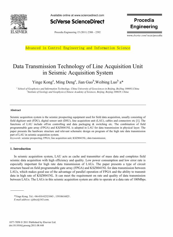
Fig. 2. The write timing between FPGA and KSZ8041NL
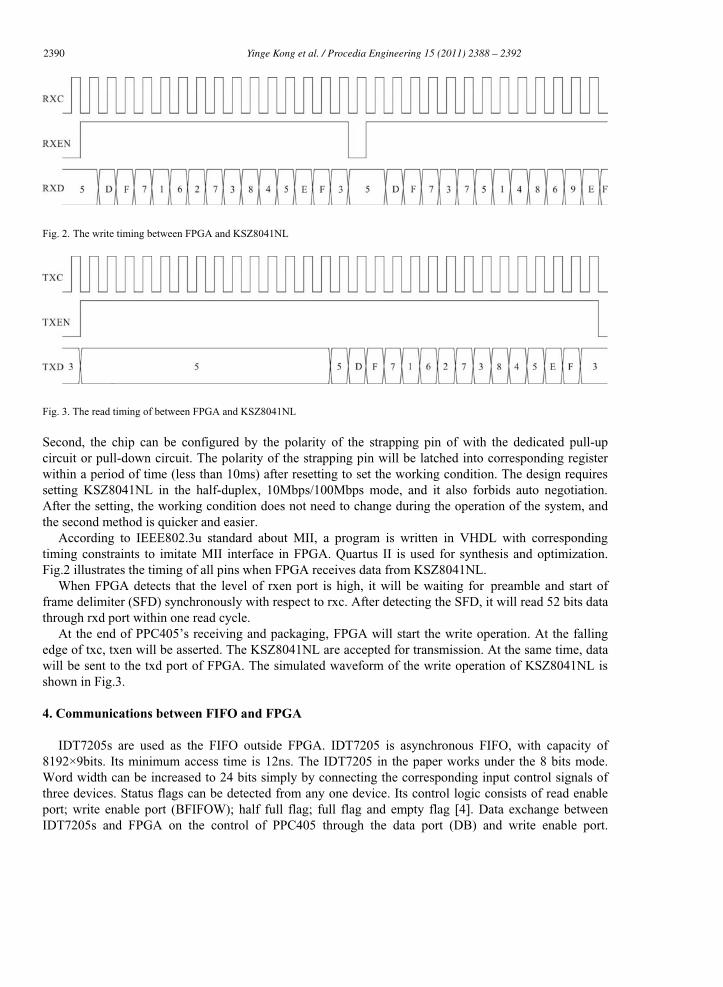
Fig. 3. The read timing of between FPGA and KSZ8041NL
Second, the chip can be configured by the polarity of the strapping pin of with the dedicated pull-up circuit or pull-down circuit. The polarity of the strapping pin will be latched into corresponding register within a period of time (less than 10ms) after resetting to set the working condition. The design requires setting KSZ8041NL in the half-duplex, 10Mbps/100Mbps mode, and it also forbids auto negotiation. After the setting, the working condition does not need to change during the operation of the system, and the second method is quicker and easier.
According to IEEE802.3u standard about MII, a program is written in VHDL with corresponding timing constraints to imitate MII interface in FPGA. Quartus II is used for synthesis and optimization. Fig.2 illustrates the timing of all pins when FPGA receives data from KSZ8041NL.
When FPGA detects that the level of rxen port is high, it will be waiting for preamble and start of frame delimiter (SFD) synchronously with respect to rxc. After detecting the SFD, it will read 52 bits data through rxd port within one read cycle.
At the end of PPC405’s receiving and packaging, FPGA will start the write operation. At the falling edge of txc, txen will be asserted. The KSZ8041NL are accepted for transmission. At the same time, data will be sent to the txd port of FPGA. The simulated waveform of the write operation of KSZ8041NL is shown in Fig.3.
4. Communications between FIFO and FPGA
IDT7205s are used as the FIFO outside FPGA. IDT7205 is asynchronous FIFO, with capacity of 8192×9bits. Its minimum access time is 12ns. The IDT7205 in the paper works under the 8 bits mode. Word width can be increased to 24 bits simply by connecting the corresponding input control signals of three devices. Status flags can be detected from any one device. Its control logic consists of read enable port; write enable port (BFIFOW); half full flag; full flag and empty flag [4]. Data exchange between IDT7205s and FPGA on the control of PPC405 through the data port (DB) and write enable port.

2391Yinge Kong et al. / Procedia Engineering 15 (2011) 2388 – 23924 Yinge Kong ,et al/ Procedia Engineering 00 (2011) 000–000
Fig. 4. The write timing between FPGA and IDT7205
After half of the memory is filled, and at the falling edge of the next write operation [4], the Half-Full Flag (HF) will be set to low before the start of the packet transmission. Packet transmission requires certain redundancy added into every packet to make it larger than half of the memory. The simulated waveform of the write cycle of IDT7205 is shown in Fig.4. The read operation of IDT7205 is completed by PPC405 through PC104 bus.
FIFO inside FPGA is generated by MegaWizard Plug-In Manager in the Quartus II software. The clock uncertainty features in Quartus II software can be used to compensate for the variable delays between clock domains [5]. FIFO with proper capacity can be selected according to the quantity of the logical resources in FPGA. The paper adopts dual-clock FIFO with different output width. Its control logic consists of read clock port, read enable flag, 16 bits data input port, write clock port, write enable flag, 32 bits data output port and a significant flag showing the number of words stored in the FIFO[6]. The read and write signals are synchronized to the read clock and write clock respectively. Because of the output latency of the read and write status signals, the significant flag is used to decide the moment to start or to close the read operation of the FIFO. While read operation is completed, the empty port is asserted [7]. An empty interrupt flag will be generated for PPC405. After detecting the empty interrupt signal of FIFO, PPC405 will write data including packed effective data, start mark of the data packet and end mark of the data packet into FPGA. The data will first go through primary buffer after entering FPGA, and then enter FIFO. Delay line is added between clock output of PPC405 and read clock port of FIFO to compensate the delay in data path [8].
5. Conclusions
The paper combines KSZ8041NL and FPGA together and applies them into seismic acquisition system, taking advantage of the ability of KSZ8041NL in high rate data transmission and the parallel operation of FPGA to ensure rapid and correct upload of the acquired data into the cross station. After actual test, the rate of data transmission in effect reached 10Mbps, the LAUs transmitted 10,000 packets of seismic data which also go through about 30 FDUs, without data error or packet loss during transmission. In cases which require higher rate of data transmission, KSZ8041NL can be allocated under 100BASE-TX transmission mode, with an appropriate cable; the transmission rate can increase to a higher data rate. The LAUs have operated at a rate of 100Mbps with the customized foil twisted pair.
Acknowledgements
This work is supported by the National "863" Program in the Eleventh Five-Year-Plan (No. 2008AA062001), and the National "863" Program in the Eleventh Five-Year-Plan (No. 2006AA09A304).
2392 Yinge Kong et al. / Procedia Engineering 15 (2011) 2388 – 2392 Yinge Kong / Procedia Engineering 00 (2011) 000–000 5
It is supported by Key Laboratory of Geo-detection (China University of Geosciences, Beijing), Ministry of Education (GDL0601).
References
[1] Sercel Company. 428XL Training Course Guide. 2008.
[2] Deng M., Wei W.B., Tang H.D., Jin S., Dong H.B., Deng J.W.. Collector for seafloor magnetotelluric data. Chinese Journal
of Geophysics 2003;46(2):217-223.
[3] Micrel Inc. KSZ8041NL 10Base-T/100Base-TX Physical Layer Transceiver Data Sheet Rev. 1.2. www.micrel.com; 2008.[4] Integrated Device Technology Inc. IDT CMOS Asynchronous FIFO. www.idt.com; 2002.
[5] Altera Inc. Quartus II Handbook Version 10.0. www.altera.com; 2010.
[6] Altera Inc. SCFIFO and DCFIFO Megafunctions User Guide. www.altera.com; 2010.
[7] Zhang Q.S., Deng M., Luo F., Qiao D.X., Chen K.. Circuit drivers of signal-acquiring unit in seafloor magnetotelluric
system. Progress in Geophysics 2004;19(4):789-793.
[8] Zhang Q.S., Deng M.,Chen K., Wang M.. Circuit Drivers Design and Hardware Realization of Acquiring Seafloor
Environment. Earth Science(Journal of China University of Geosciences) 2007;32(4):499-503.