Embed Size (px)
Citation preview
FACULDADE DE ENGENHARIA DA UNIVERSIDADE DO PORTO
DC/DC Converter with TransparentElectronics for application on
Photovoltaic Panels
Romano Jorge de Sousa Torres
PREPARAÇÃO DA DISSERTAÇÃO
PREPARAÇÃO DA DISSERTAÇÃO
Orientador: Vitor Grade Tavares (PhD)
Co-orientador: Pedro Miguel Cândido Barquinha (PhD)
Co-orientador: Ganga Mamba Bahubalindruni
February 13, 2013

c© Romano Jorge de Sousa Torres, 2013
DC/DC Converter with Transparent Electronics forapplication on Photovoltaic Panels
Romano Jorge de Sousa Torres
PREPARAÇÃO DA DISSERTAÇÃO
February 13, 2013

Sumário
A eletrónica transparente é uma tecnologia emergente que pode proporcionar sistemas de baixocusto dada a possibilidade de fabricação de dispositivos a baixa temperatura. A sua aplicação podeser útil em vários domínios como indumentária eletrónica e sensores de monitorização de saúde.Com a implementação de conversores DC/DC em eletrónica transparente, as aplicações poderiamextender-se para dispositivos com fonte de bateria ou painéis fotovoltáicos.
A tecnologia transparente é baseada em transístores de filme fino (TFT) com semicondutores a-IGZO, material que emergiu nos últimos anos. Os transístores podem ser utilizados para a criaçãodo Conversor DC/DC desejado, o qual pode ser depositado do vidro dos painéis, reduzindo oscustos de montagem e conceção de todo o sistema.
Esta dissertação tem como principal objetivo o projeto e desenvolvimento para construçãode uma topologia de conversor DC/DC com eletrónica transparente para aplicação em painéisfotovoltáicos. Inclui o estudo de elementos passivos, como bobinas e condensadores, e a suapossibilidade de utilização.
O trabalho tem a colaboração do grupo CENIMAT da Universidade Nova de Lisboa. Nesselocal será construído o conversor DC/DC e os circuitos desenvolvidos durante esta dissertação.
i

ii
Abstract
Transparent electronics is a forthcoming technology, which allows for low-cost systems with de-vices fabricated at low temperatures. Its applications may be useful in various domains, suchas wearable electronics and sensors for health monitoring. Designing DC/DC converters withtransparent technology, the possible applications could extend to battery supplied devices or pho-tovoltaic panels.
Transparent technology, in this work, is based on thin-film transistors (TFT) with a-IGZOsemiconductors, material that has emerged in recent years. Their effectiveness for designingDC/DC converters will be assessed. Such converter could eventually be deposited on the glasscasing of photovoltaic panels, reducing installation and designing costs of the whole system.
This dissertation has in its main objective the development, design and fabrication of a DC/DCconverter topology with transparent electronics, for application in photovoltaic panels. It includesthe study of some passive elements, such as inductors and capacitors, and their effectiveness for apossible use.
The work is developed in collaboration with the CENIMAT group at UNL, where the devel-oped circuits and DC/DC converter will be fabricated.
iii

iv
Contents
1 Introduction 11.1 Motivation . . . . . . . . . . . . . . . . . . . . . . . . . . . . . . . . . . . . . . 11.2 Generic Proposed Solution . . . . . . . . . . . . . . . . . . . . . . . . . . . . . 21.3 Structure of the Document . . . . . . . . . . . . . . . . . . . . . . . . . . . . . 2
2 Background 32.1 DC/DC Converters . . . . . . . . . . . . . . . . . . . . . . . . . . . . . . . . . 3
2.1.1 Step-Down Buck Converter . . . . . . . . . . . . . . . . . . . . . . . . 32.1.2 Step-Up Boost Converter . . . . . . . . . . . . . . . . . . . . . . . . . . 42.1.3 Buck-Boost Converter . . . . . . . . . . . . . . . . . . . . . . . . . . . 42.1.4 Cuk converter . . . . . . . . . . . . . . . . . . . . . . . . . . . . . . . . 5
2.2 Transparent electronic devices . . . . . . . . . . . . . . . . . . . . . . . . . . . 62.2.1 Resistors . . . . . . . . . . . . . . . . . . . . . . . . . . . . . . . . . . 62.2.2 Capacitors . . . . . . . . . . . . . . . . . . . . . . . . . . . . . . . . . 62.2.3 Inductors . . . . . . . . . . . . . . . . . . . . . . . . . . . . . . . . . . 72.2.4 Thin-film transistors (TFT) . . . . . . . . . . . . . . . . . . . . . . . . . 72.2.5 Fabrication processes . . . . . . . . . . . . . . . . . . . . . . . . . . . . 11
2.3 Voltage Multipliers . . . . . . . . . . . . . . . . . . . . . . . . . . . . . . . . . 122.3.1 Charge-Pump Step-Up Converter . . . . . . . . . . . . . . . . . . . . . 132.3.2 Charge-Pump Step-Down Converter . . . . . . . . . . . . . . . . . . . . 142.3.3 Improved Circuit Designs . . . . . . . . . . . . . . . . . . . . . . . . . 15
3 Bibliographic Review 193.1 Thin-Film Transistors using a-IGZO . . . . . . . . . . . . . . . . . . . . . . . . 193.2 An Overview on DC/DC Converters using Transparent Electronics . . . . . . . . 20
3.2.1 Switched-Capacitor based Embedded DC-DC Buck Converter . . . . . . 203.2.2 DC/DC Converters using Indium Gallium Zinc Oxide Thin-Film Transistors 213.2.3 DC/DC Converters in Organic Thin-Film Transistor Technology . . . . . 23
4 Specifications 254.1 Proposal for Boost DC/DC Converter . . . . . . . . . . . . . . . . . . . . . . . 254.2 Proposal for Buck DC/DC Converter . . . . . . . . . . . . . . . . . . . . . . . . 26
5 Conclusions and Future Work 27
v

vi CONTENTS
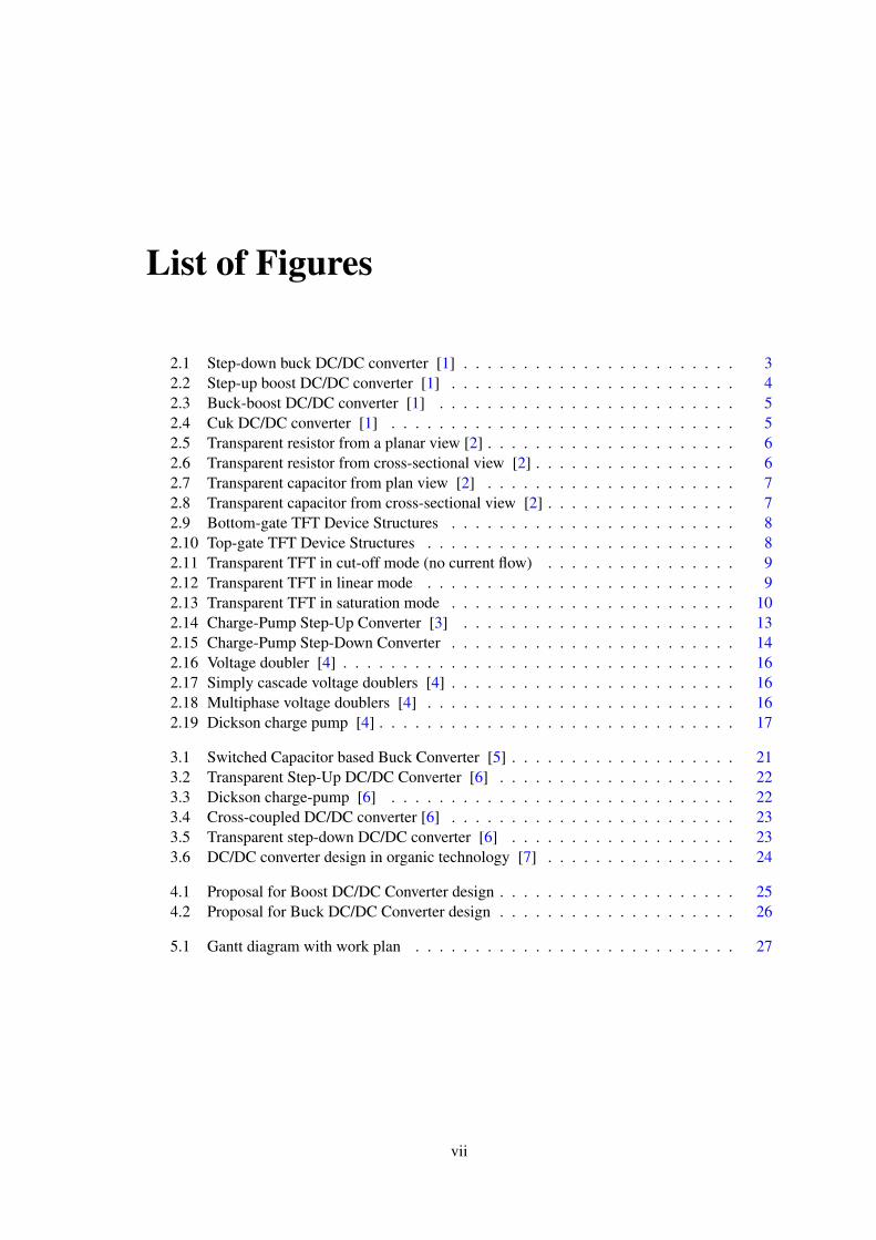
List of Figures
2.1 Step-down buck DC/DC converter [1] . . . . . . . . . . . . . . . . . . . . . . . 32.2 Step-up boost DC/DC converter [1] . . . . . . . . . . . . . . . . . . . . . . . . 42.3 Buck-boost DC/DC converter [1] . . . . . . . . . . . . . . . . . . . . . . . . . 52.4 Cuk DC/DC converter [1] . . . . . . . . . . . . . . . . . . . . . . . . . . . . . 52.5 Transparent resistor from a planar view [2] . . . . . . . . . . . . . . . . . . . . . 62.6 Transparent resistor from cross-sectional view [2] . . . . . . . . . . . . . . . . . 62.7 Transparent capacitor from plan view [2] . . . . . . . . . . . . . . . . . . . . . 72.8 Transparent capacitor from cross-sectional view [2] . . . . . . . . . . . . . . . . 72.9 Bottom-gate TFT Device Structures . . . . . . . . . . . . . . . . . . . . . . . . 82.10 Top-gate TFT Device Structures . . . . . . . . . . . . . . . . . . . . . . . . . . 82.11 Transparent TFT in cut-off mode (no current flow) . . . . . . . . . . . . . . . . 92.12 Transparent TFT in linear mode . . . . . . . . . . . . . . . . . . . . . . . . . . 92.13 Transparent TFT in saturation mode . . . . . . . . . . . . . . . . . . . . . . . . 102.14 Charge-Pump Step-Up Converter [3] . . . . . . . . . . . . . . . . . . . . . . . 132.15 Charge-Pump Step-Down Converter . . . . . . . . . . . . . . . . . . . . . . . . 142.16 Voltage doubler [4] . . . . . . . . . . . . . . . . . . . . . . . . . . . . . . . . . 162.17 Simply cascade voltage doublers [4] . . . . . . . . . . . . . . . . . . . . . . . . 162.18 Multiphase voltage doublers [4] . . . . . . . . . . . . . . . . . . . . . . . . . . 162.19 Dickson charge pump [4] . . . . . . . . . . . . . . . . . . . . . . . . . . . . . . 17
3.1 Switched Capacitor based Buck Converter [5] . . . . . . . . . . . . . . . . . . . 213.2 Transparent Step-Up DC/DC Converter [6] . . . . . . . . . . . . . . . . . . . . 223.3 Dickson charge-pump [6] . . . . . . . . . . . . . . . . . . . . . . . . . . . . . 223.4 Cross-coupled DC/DC converter [6] . . . . . . . . . . . . . . . . . . . . . . . . 233.5 Transparent step-down DC/DC converter [6] . . . . . . . . . . . . . . . . . . . 233.6 DC/DC converter design in organic technology [7] . . . . . . . . . . . . . . . . 24
4.1 Proposal for Boost DC/DC Converter design . . . . . . . . . . . . . . . . . . . . 254.2 Proposal for Buck DC/DC Converter design . . . . . . . . . . . . . . . . . . . . 26
5.1 Gantt diagram with work plan . . . . . . . . . . . . . . . . . . . . . . . . . . . 27
vii

viii LIST OF FIGURES

List of Tables
3.1 Simulated results of negative DC/DC converters with load current . . . . . . . . 24
ix

x LIST OF TABLES

Abreviaturas e Símbolos
a-IGZO amorphous Indium Gallium Zinc OxideDC Direct currentFEUP Faculdade de Engenharia da Universidade do PortoITO Indium Tin OxideMOSFET Metal Oxide Semiconductor Field Effect TransistorMPDV Multiphase voltage doublerTFT Thin-Film TransistorTPVD Two-phase voltage doublerUNL Universidade Nova de LisboaUV Ultra-violet
xi

Chapter 1
Introduction
The main focus of this thesis is the study and implementation of DC/DC converters with transpar-
ent electronics. Transparent electronics is a forthcoming technology that promises cost effective
solutions and opens a new set possibilities, such as electronics on glass. The discover of fabri-
cation processes at low temperature, allows the development of TFT on flexible substrates at an
evermore low cost. The transparent DC/DC converters can be used on photovoltaic panels by
deposition on glass.
1.1 Motivation
Today, there are many studies concerning climate changes that result from the burning of non-
renewable energy sources, causing emissions of carbon dioxide to atmosphere and developing
greenhouse effect. Due to an increasing world population, the energy demand rises, depleting
petroleum and other non-renewable energy sources. The research on alternative and renewable
energy sources is then of outmost importance. Photovoltaic energy is one possibility.
Photovoltaic panels often use DC/DC Converters. They are mainly electronic circuits that
change the voltage value from input to output, working with direct currents (dc). Their application
extend to battery supplied devices, like mobile phones, laptops, typically to increase the voltage
provided. Converters are used also on photovoltaic panels. In this case, the converter produces a
regulated output voltage from energy temporarily saved, releasing it on a different voltage value,
with increasing efficiency.
Now-a-days, the inclusion of photovoltaic panels on daily life is possible, by either using the
roofs of buildings or large fields, but the creation of transparent devices can be considered as a
possibility of embodying the electronics with panels. Such approach could effectively down-size
the overall cost of the electronics (low-temperature fabrication) and of assembly (deposition of
electronic system on the glass casing). This is the main motivation behind the present proposal for
dissertation.
1
2 Introduction
1.2 Generic Proposed Solution
The first proposal described in this report, for a possible DC/DC converter topology to be imple-
mented with transparent electronics, uses switched-capacitor concepts to circumvent the need for
inductive elements. However, there are other issues that need to be taking into account. This report
presents in chapter 4 the main difference between a positive and negative DC/DC converter of this
type, describing the ideal behaviour expected from each topology.
1.3 Structure of the Document
Besides the introduction, this report has 4 more chapters.
Chapter 2 discusses the fundamentals and theory behind the construction of DC/DC converters
with transparent electronics.
Chapter 3 presents the state of the art, where various studies, closely related to the goal of this
dissertation, are exposed.
Chapter 4 presents the specifications and an initial approach to the desired converter.
Chapter 5 presents the conclusions and the work plan for the thesis.
Chapter 2
Background
2.1 DC/DC Converters
M. Rashid [1] describes DC/DC Converters as electronic circuits that receive an input voltage,
increase or decrease its level, resulting in a different voltage level at the output. They are important
for electronic voltage-supply systems.
Linear power regulators are systems that impose a steady and constant voltage at the output,
with a changing (and different) voltage level at input. Linear regulators are limited to an output
voltage level smaller than the input, but their power efficiency is in general reasonably small.
Switched-mode regulators are another way to get an output voltage level different from input.
They use on and off states to achieve good efficiency.
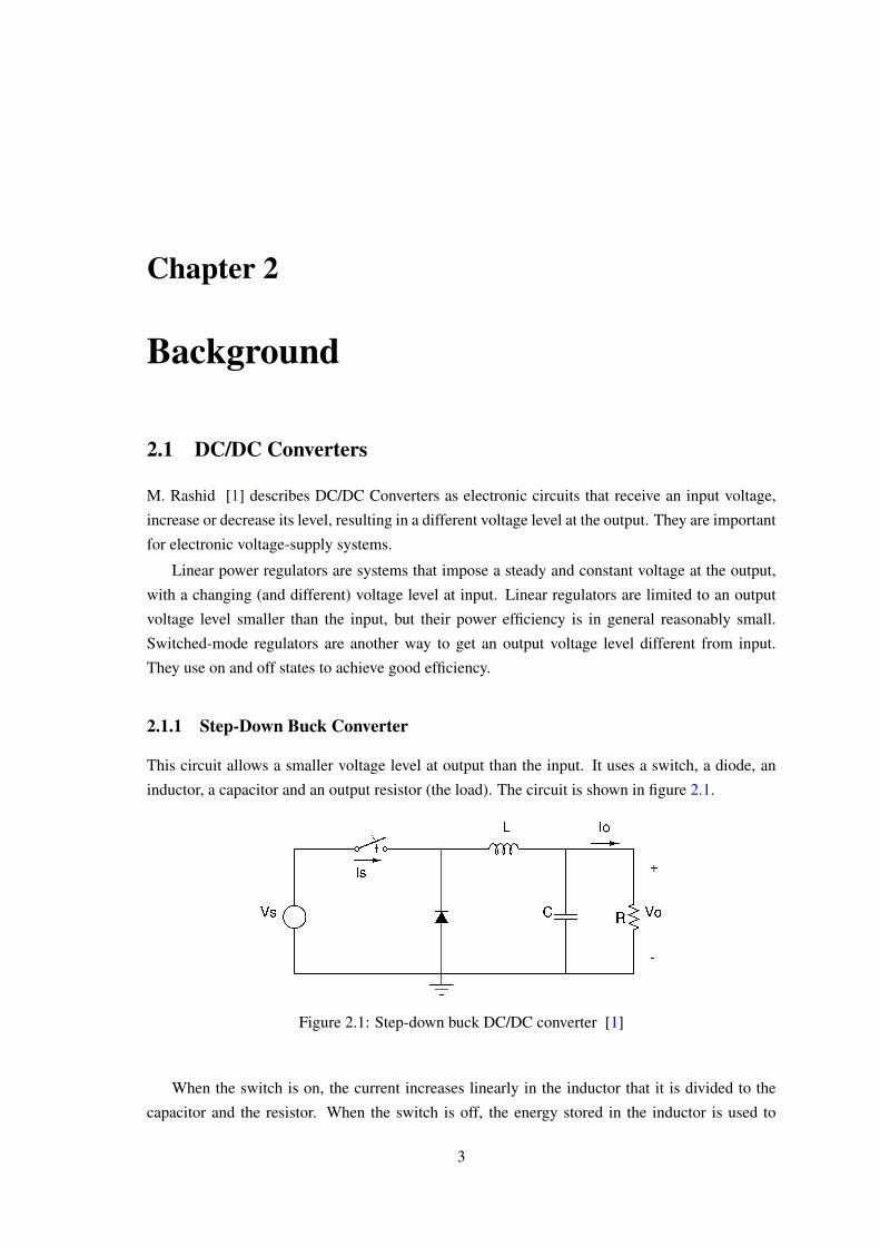
2.1.1 Step-Down Buck Converter
This circuit allows a smaller voltage level at output than the input. It uses a switch, a diode, an
inductor, a capacitor and an output resistor (the load). The circuit is shown in figure 2.1.
Figure 2.1: Step-down buck DC/DC converter [1]
When the switch is on, the current increases linearly in the inductor that it is divided to the
capacitor and the resistor. When the switch is off, the energy stored in the inductor is used to
3

4 Background
feed the output, and the current flows throw the diode which decreases linearly and smoothly. The
frequency of switching allows an adequate constant voltage level at the output.
The average output voltage level can be determined by the duty cycle "D" — the ratio between
time when the switch is on and the period. The following equation [1] shows the relation between
the output and input voltages for this Step-Down Buck Converter, calculated by Faraday’s Law:
Vout
Vin= D (2.1)
The output voltage is always smaller than the input, given the fact that the duty cycle "D" value
is smaller than 1.
2.1.2 Step-Up Boost Converter
This circuit allows an output voltage level greater than the input. It uses the same devices as the
Buck converter, but the layout changes the characteristics. The circuit can be seen in figure 2.2.
Figure 2.2: Step-up boost DC/DC converter [1]
When the switch is on, the current in the inductor increases, and energy is stored. The diode
is off, and the capacitor feeds the load. When the switch goes to off, the energy in the inductor
is released to the capacitor and resistor. The average voltage ratio is also determined by the duty
cycle, resulting in higher output voltage level:
Vout
Vin=
11−D
(2.2)
2.1.3 Buck-Boost Converter
It was created to allow an output voltage level greater or smaller than the input, depending of duty
cycle. The circuit can be seen in figure 2.3.
2.1 DC/DC Converters 5
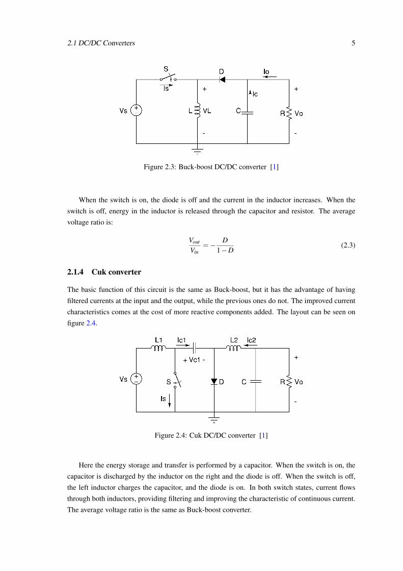
Figure 2.3: Buck-boost DC/DC converter [1]
When the switch is on, the diode is off and the current in the inductor increases. When the
switch is off, energy in the inductor is released through the capacitor and resistor. The average
voltage ratio is:
Vout
Vin=− D
1−D(2.3)
2.1.4 Cuk converter
The basic function of this circuit is the same as Buck-boost, but it has the advantage of having
filtered currents at the input and the output, while the previous ones do not. The improved current
characteristics comes at the cost of more reactive components added. The layout can be seen on
figure 2.4.
Figure 2.4: Cuk DC/DC converter [1]
Here the energy storage and transfer is performed by a capacitor. When the switch is on, the
capacitor is discharged by the inductor on the right and the diode is off. When the switch is off,
the left inductor charges the capacitor, and the diode is on. In both switch states, current flows
through both inductors, providing filtering and improving the characteristic of continuous current.
The average voltage ratio is the same as Buck-boost converter.

6 Background
2.2 Transparent electronic devices
DC/DC converters use various components such as resistors, capacitors, diodes and inductors.
Regarding the goal of creation such device with transparent electronics, a study about transparency
is very important.
To create transparent devices, different materials should be combined to perform the functions
of non-transparent devices. The efficiency of new devices created should be, as possible, equal
or better to the existing ones. However, the characteristics of transparent electronic materials
comparing with the others, like smaller conductivity, decrease their efficiency.
There have been many studies to create high performance devices. They focus on the layout
of materials, and the results are sometimes very different from what could be expected with non-
transparency.
2.2.1 Resistors
According to D. Keszler et al. [2], a good performance resistor should fulfil the characteristic
defined by Ohm’s law; it should have a linear behaviour according to this law. Parasitic capacitance
is undesirable, therefore those should be fabricated on insulating substrates.
Taking advantage of the smaller conductivity of transparent materials, resistors are created
with a long path between two contacts. The layout can be seen in figures 2.5 and 2.6.
Figure 2.5: Transparent resistor from a planar view [2]
Figure 2.6: Transparent resistor from cross-sectional view [2]
The passivation layer is created to protect the resistor physically and chemically. Hence, the
conductance of resistor establishes. The resistance value is proportional to the resistivity of mate-
rial and the path length. It is inversely proportional to the width.
2.2.2 Capacitors
Capacitors should have a linear current-voltage derivative characteristic, according to D. Keszler
et al. [2]. They are created to store energy in an electric field form. A transparent capacitor can
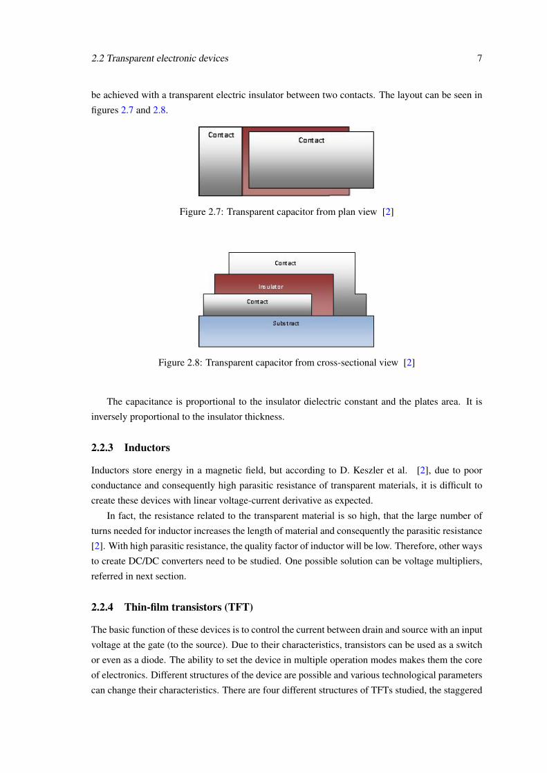
2.2 Transparent electronic devices 7
be achieved with a transparent electric insulator between two contacts. The layout can be seen in
figures 2.7 and 2.8.
Figure 2.7: Transparent capacitor from plan view [2]
Figure 2.8: Transparent capacitor from cross-sectional view [2]
The capacitance is proportional to the insulator dielectric constant and the plates area. It is
inversely proportional to the insulator thickness.
2.2.3 Inductors
Inductors store energy in a magnetic field, but according to D. Keszler et al. [2], due to poor
conductance and consequently high parasitic resistance of transparent materials, it is difficult to
create these devices with linear voltage-current derivative as expected.
In fact, the resistance related to the transparent material is so high, that the large number of
turns needed for inductor increases the length of material and consequently the parasitic resistance
[2]. With high parasitic resistance, the quality factor of inductor will be low. Therefore, other ways
to create DC/DC converters need to be studied. One possible solution can be voltage multipliers,
referred in next section.
2.2.4 Thin-film transistors (TFT)
The basic function of these devices is to control the current between drain and source with an input
voltage at the gate (to the source). Due to their characteristics, transistors can be used as a switch
or even as a diode. The ability to set the device in multiple operation modes makes them the core
of electronics. Different structures of the device are possible and various technological parameters
can change their characteristics. There are four different structures of TFTs studied, the staggered
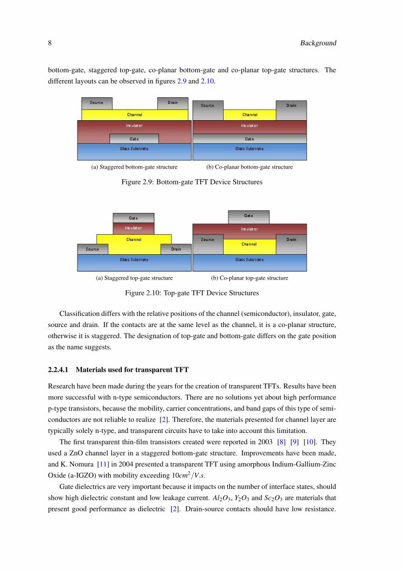
8 Background
bottom-gate, staggered top-gate, co-planar bottom-gate and co-planar top-gate structures. The
different layouts can be observed in figures 2.9 and 2.10.
(a) Staggered bottom-gate structure (b) Co-planar bottom-gate structure
Figure 2.9: Bottom-gate TFT Device Structures
(a) Staggered top-gate structure (b) Co-planar top-gate structure
Figure 2.10: Top-gate TFT Device Structures
Classification differs with the relative positions of the channel (semiconductor), insulator, gate,
source and drain. If the contacts are at the same level as the channel, it is a co-planar structure,
otherwise it is staggered. The designation of top-gate and bottom-gate differs on the gate position
as the name suggests.
2.2.4.1 Materials used for transparent TFT
Research have been made during the years for the creation of transparent TFTs. Results have been
more successful with n-type semiconductors. There are no solutions yet about high performance
p-type transistors, because the mobility, carrier concentrations, and band gaps of this type of semi-
conductors are not reliable to realize [2]. Therefore, the materials presented for channel layer are
typically solely n-type, and transparent circuits have to take into account this limitation.
The first transparent thin-film transistors created were reported in 2003 [8] [9] [10]. They
used a ZnO channel layer in a staggered bottom-gate structure. Improvements have been made,
and K. Nomura [11] in 2004 presented a transparent TFT using amorphous Indium-Gallium-Zinc
Oxide (a-IGZO) with mobility exceeding 10cm2/V.s.
Gate dielectrics are very important because it impacts on the number of interface states, should
show high dielectric constant and low leakage current. Al2O3, Y2O3 and Sc2O3 are materials that
present good performance as dielectric [2]. Drain-source contacts should have low resistance.
2.2 Transparent electronic devices 9
P.Barquinha et al. [12] suggests the usage of molybdenum (Mo) or Ti/Au contacts due to their
good characteristics.
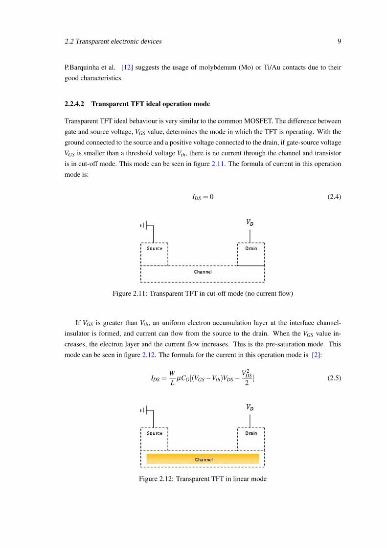
2.2.4.2 Transparent TFT ideal operation mode
Transparent TFT ideal behaviour is very similar to the common MOSFET. The difference between
gate and source voltage, VGS value, determines the mode in which the TFT is operating. With the
ground connected to the source and a positive voltage connected to the drain, if gate-source voltage
VGS is smaller than a threshold voltage Vth, there is no current through the channel and transistor
is in cut-off mode. This mode can be seen in figure 2.11. The formula of current in this operation
mode is:
IDS = 0 (2.4)
Figure 2.11: Transparent TFT in cut-off mode (no current flow)
If VGS is greater than Vth, an uniform electron accumulation layer at the interface channel-
insulator is formed, and current can flow from the source to the drain. When the VGS value in-
creases, the electron layer and the current flow increases. This is the pre-saturation mode. This
mode can be seen in figure 2.12. The formula for the current in this operation mode is [2]:
IDS =WL
µCG[(VGS−Vth)VDS−V 2
DS2
] (2.5)
Figure 2.12: Transparent TFT in linear mode
10 Background
where W is the gate width (µm), L is the gate length (µm), µ is the channel mobility (cm2/V.s),
CG is the gate capacitance density (F/cm2), VGS is the gate-source voltage (V), Vth is threshold
voltage (V) and VDS is drain-source voltage (V).
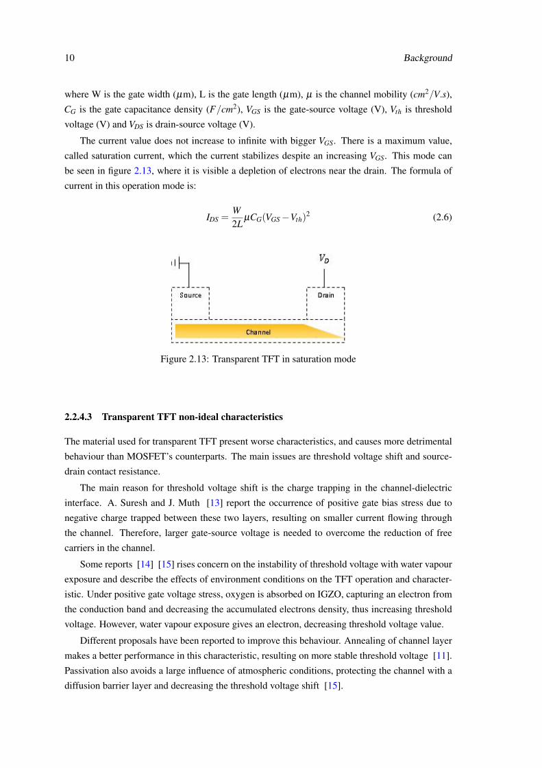
The current value does not increase to infinite with bigger VGS. There is a maximum value,
called saturation current, which the current stabilizes despite an increasing VGS. This mode can
be seen in figure 2.13, where it is visible a depletion of electrons near the drain. The formula of
current in this operation mode is:
IDS =W2L
µCG(VGS−Vth)2 (2.6)
Figure 2.13: Transparent TFT in saturation mode
2.2.4.3 Transparent TFT non-ideal characteristics
The material used for transparent TFT present worse characteristics, and causes more detrimental
behaviour than MOSFET’s counterparts. The main issues are threshold voltage shift and source-
drain contact resistance.
The main reason for threshold voltage shift is the charge trapping in the channel-dielectric
interface. A. Suresh and J. Muth [13] report the occurrence of positive gate bias stress due to
negative charge trapped between these two layers, resulting on smaller current flowing through
the channel. Therefore, larger gate-source voltage is needed to overcome the reduction of free
carriers in the channel.
Some reports [14] [15] rises concern on the instability of threshold voltage with water vapour
exposure and describe the effects of environment conditions on the TFT operation and character-
istic. Under positive gate voltage stress, oxygen is absorbed on IGZO, capturing an electron from
the conduction band and decreasing the accumulated electrons density, thus increasing threshold
voltage. However, water vapour exposure gives an electron, decreasing threshold voltage value.
Different proposals have been reported to improve this behaviour. Annealing of channel layer
makes a better performance in this characteristic, resulting on more stable threshold voltage [11].
Passivation also avoids a large influence of atmospheric conditions, protecting the channel with a
diffusion barrier layer and decreasing the threshold voltage shift [15].
2.2 Transparent electronic devices 11
Some studies are also concerned with the effects of temperature and light on threshold voltage
shift, which is very important to refer due to the specific application in question — photovoltaic
panels. S. Kuk et al. [16] report an increase from 0.89 V to 4.35 V as light temperature increases
from 30oC to 90oC, explaining the donation of electrons to the conduction band as reason for so
large increase. Light illumination enhances the charge trapping.
S. Lee et al. [17] refer a threshold voltage shift in 7000 seconds by less than 1 V in dark state,
but an 8.7 V shift with 400 nm light and intensity of 0.025mW/cm2, when a negative bias stress
is applied. However, they also report a saturation value for the shift, caused by the filling of the
available charge-trapping states to the full.
Threshold voltage shift is an increasing problem if the transistor is conducting for a long time.
DC/DC converters use clock signals to open or close the transistor as a switch, so the transistor
will not have a large time of conduction and threshold voltage shift will not be the main problem
to concern.
Another possible reason of concern with TFTs is the source-drain contact resistance. Accord-
ing to P. Barquinha et al. [12], source-drain contact resistance is a phenomenon that affects the
performance of thin-film transistor, mainly the mobility of short channel devices, because the over-
lap between contacts and the channel may not be negligible when compared to the length of the
channel. They report higher maximum current in linear and saturation modes with molybdenum
(Mo) or Ti/Au contacts. They also refer an improvement on maximum current and field-effect
mobility with annealing after placing source-drain contacts. Source-drain contact resistance can
decrease the current flowing through a closed transistor, creating a voltage drop. For a boost
converter, a high voltage drop can result in a low voltage level at the output.
2.2.5 Fabrication processes
Since the appearance of transparent thin-film transistors that research is made to improve the
fabrication processes. The goal is to achieve more precision and control of thickness and layout,
when the thin-film is created. The fabrication processes of transparent devices include pulsed
laser deposition, photolithography, etching, chemical layer deposition, atomic layer deposition
and physical vapour deposition.
2.2.5.1 Pulsed laser deposition
K. Nomura et al. [11] report this technique in the first TFT created. It is used for deposition
of indium gallium zinc oxide (IGZO) and indium tin oxide (ITO) thin films. Inside a vacuum
chamber, a high and short energy laser pulses collide on a solid target, typically ceramic. The
laser pulse beam creates a phenomenon of vaporization of the target. The vapour condenses, and
generates a thin film on the substrate.
12 Background
2.2.5.2 Photolithography
It is the process of transferring images from the computer database to the wafer. Initially, it is used
a computer-aided design system to draw the layer. Then, a photoresist is exposed to ultraviolet
light, which make its material characteristics to be altered. A photomask is used to create the
pattern where it is opaque or transparent to UV light.
2.2.5.3 Etching
This process removes the exposed material created on photolithography to refine the desired pat-
tern. This can be achieved by wet etching, where acids are used to remove the material depending
on the time and temperature it is exposed, and dry etching, where the material is exposed to a
bombardment of ions, and portions of material are removed selectively.
2.2.5.4 Chemical layer deposition
Technique obtained by the introduction of chemical gases on a chamber, which reacts with the
wafer in order to design the thin film. This makes a flow system, where reactant gases flow into
the substrate and products are removed from it.
2.2.5.5 Atomic layer deposition
The thin-film layers are obtained from a sequential exposure of precursors, or chemical gases,
reacting with the substrate. It is a self-limiting process, which enables a control on growth depo-
sition and uniformity even on large areas, and it differentiates from chemical layer deposition due
to the separation of precursors by inert gas during reaction.
2.2.5.6 Physical vapour deposition
These processes create deposition of atoms from a source onto a substrate. The two mainly pro-
cesses of this type are evaporation and sputtering. In the first, it is created by a resistive heating
with electric current. While the material is melting and evaporating, the vapour material con-
denses, creating the thin film. The second one, sputtering, uses the collision of gaseous ions to
dislodge atoms while thin film is deposited. It is a very controllable technique in terms of thickness
of the film, and very used nowadays. CENIMAT, a Portuguese scientific research centre, uses the
RF sputtering technique [18]. It utilizes energy from radio waves to ionize the gas atoms. Further,
the ions get in contact with the substrate, creating the film.
2.3 Voltage Multipliers
Voltage multipliers use capacitors and switches or diodes to achieve a different output voltage.
The principle of operation is to store energy in capacitors, charging and discharging, transferring
it to the output load [4]. The study of these devices can be important for the implementation

2.3 Voltage Multipliers 13
of transparent DC/DC converter, because it could enable the desired functionalities of a normal
DC/DC converter without using inductors, avoiding the problems referred in the last section.
2.3.1 Charge-Pump Step-Up Converter
This circuit returns a higher voltage at output than received at the input. M. Wens and M. Steyaert
[3] present an example of charge-pump step-up DC-DC converter based on a voltage doubler, as
shown in figure 2.14.
Figure 2.14: Charge-Pump Step-Up Converter [3]
When the switches are at position 1, the voltage source charges capacitor C1. CL discharges
to RL. When the switches are at position 2, the lower terminal of C1 connects in series with the
voltage source, and CL and RL receive charge from the both. Hence, the output voltage is higher
than the input. Makowski in [4] refers that the Vout/Vin ratio is limited by 2n, where n is the
number of capacitors used.
M. Wens and M.Steyaert [3] estimate the output voltage for ideal converter by:
Vout = RLIout = RL fSW ∆QSW = RL fSWC1∆VC1 = RL fSWC1(2Vin−Vout) (2.7)
Vout =RL fSWC1V in
1+RL f SWC1(2.8)
where fSW is the switching frequency, ∆QSW is the amount of charge being transferred to the
output in each switching cycle and ∆VC1 is the difference of voltage level between switching state
1 and 2.
The efficiency of the converter is divided by the two stages of switching. The efficiency on
first stage is calculated by the energy in C1 divided by the energy transferred to the capacitor:
ηΦ1 =EC1
EVin→C1
=Vout
2Vin(2.9)
14 Background
When C1 is discharged, the efficiency is estimated with the energy in C2 divided by the energy
transferred from source and C1 to C2:
ηΦ2 =EC2
EVinC1→C2
=2C1Vin +C1Vout +2C2Vout
4C1Vin +2C2Vin +C2Vout(2.10)
The resulting efficiency of the circuit is:
ηup = ηΦ1ηΦ2 =Vout(2C2Vout +C1(2Vin +Vout))
2Vin(4C1Vin +C2(2Vin +Vout))(2.11)
The authors [3] estimate an efficiency between 35% if Vout/Vin = 1 and 100% if Vout/Vin = 2.
2.3.2 Charge-Pump Step-Down Converter
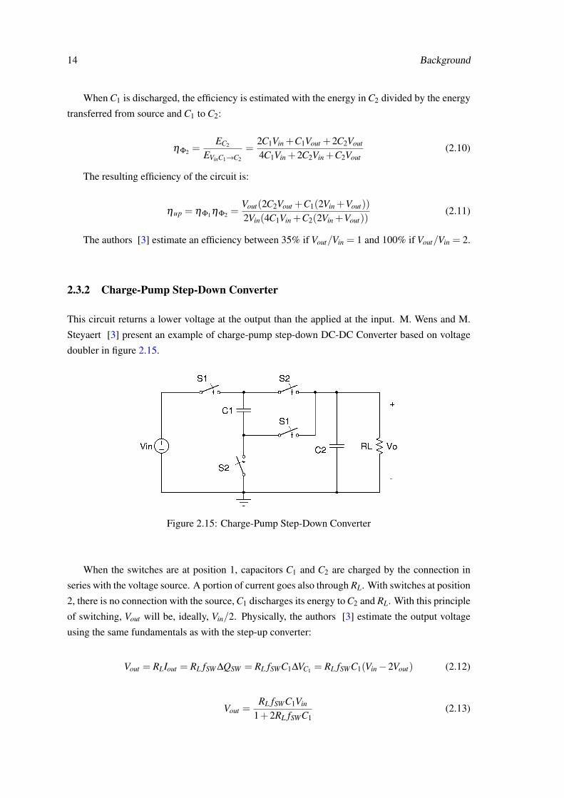
This circuit returns a lower voltage at the output than the applied at the input. M. Wens and M.
Steyaert [3] present an example of charge-pump step-down DC-DC Converter based on voltage
doubler in figure 2.15.
Figure 2.15: Charge-Pump Step-Down Converter
When the switches are at position 1, capacitors C1 and C2 are charged by the connection in
series with the voltage source. A portion of current goes also through RL. With switches at position
2, there is no connection with the source, C1 discharges its energy to C2 and RL. With this principle
of switching, Vout will be, ideally, Vin/2. Physically, the authors [3] estimate the output voltage
using the same fundamentals as with the step-up converter:
Vout = RLIout = RL fSW ∆QSW = RL fSWC1∆VC1 = RL fSWC1(Vin−2Vout) (2.12)
Vout =RL fSWC1Vin
1+2RL fSWC1(2.13)

2.3 Voltage Multipliers 15
To estimate efficiency, on the first switching position, the energy in C1 and C2 is divided by
the energy transferred from voltage source to these capacitors:
ηΦ1 =EC1C2
EVin→C1C2
=Vin +2Vout
2Vin(2.14)
On the second switching mode, efficiency is calculated by the ratio between the energy in C2
and the energy transferred from C1 to C2:
ηΦ2 =EC2
EC1→C2
=C1Vin +2C2Vout
Vin(2C1 +C2)−2C1Vout(2.15)
Total efficiency of the circuit is obtained multiplying both values:
ηup = ηΦ1ηΦ2 =(C1Vin +2C2Vout)(
Vin+2Vout2Vin
)
C2Vin +2C1(Vin−Vout)(2.16)
The same authors [3] estimate an efficiency of 100% if Vout/Vin = 0.5. This value decreases
with lower values of Vout/Vin.
2.3.3 Improved Circuit Designs
In charge-pumps based on voltage multipliers, the difference between a step-up and step-down
converter is the position of first capacitor, namely, the flying capacitor C1. As referred in last
subsections, on the second switching position, step-up converters have this capacitor connected in
series with RL and the input source. In fact, the voltage source is never disconnected from the rest
of the circuit, in contrast to step-down converters. Therefore, step-down converters have the flying
capacitor always connected to output, in opposition to the step-up that has it always connected to
the input.
The adaptation of the converter for a desired output voltage is achieved with the layout of
circuit. The position of capacitors influences the output voltage level, so the design of circuit must
take into account what is expected.
J. Starzyk [4] compare different charge-pump designs on the boosting energy required. Since
the load resistance is not infinite, the circuits do not present a perfect behaviour, such as Vout/Vin =
0.5 in step-down and Vout/Vin = 2 in step-up converter. The output voltage is as lower as the load
resistance is.
The author [4] present a two-phase voltage doubler (TPVD) with the design in figure 2.16.
The doublers can be used in cascade as represented in figure 2.17.
Removing the second capacitor in each doubler, Starzyk [4] presents a multiphase voltage
doubler (MPVD), which need half of the capacitors for the same output/input voltage ratio. The
circuit is shown in figure 2.18.
The improved charge-pumps are compared to the standard one from Dickson in figure 2.19.
Some of the Starzyk’s conclusions [4] are that the number of stages used does not affect the
output power. It depends on the load resistance, capacitors and clock frequency. When the value
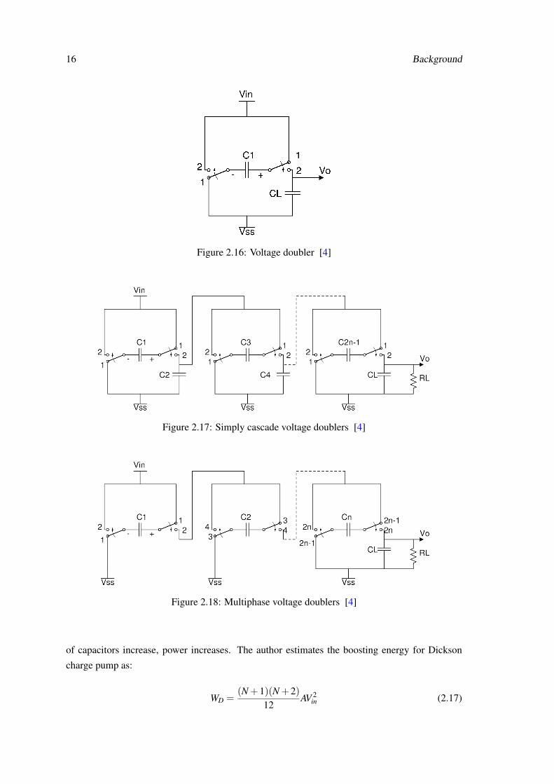
16 Background
Figure 2.16: Voltage doubler [4]
Figure 2.17: Simply cascade voltage doublers [4]
Figure 2.18: Multiphase voltage doublers [4]
of capacitors increase, power increases. The author estimates the boosting energy for Dickson
charge pump as:
WD =(N +1)(N +2)
12AV 2
in (2.17)
2.3 Voltage Multipliers 17
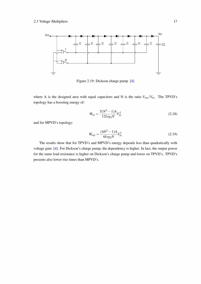
Figure 2.19: Dickson charge pump [4]
where A is the designed area with equal capacitors and N is the ratio Vout/Vin. The TPVD’s
topology has a boosting energy of:
Wt p =5(N2−1)A
12log2NV 2
in (2.18)
and for MPVD’s topology:
Wmp =(4N2−1)A
6log2NV 2
in (2.19)
The results show that for TPVD’s and MPVD’s energy depends less than quadratically with
voltage gain [4]. For Dickson’s charge pump, the dependency is higher. In fact, the output power
for the same load resistance is higher on Dickson’s charge pump and lower on TPVD’s. TPVD’s
presents also lower rise times than MPVD’s.

18 Background

Chapter 3
Bibliographic Review
There is not that many reports on transparent DC/DC Converters, but the ones that exist, invari-
ably use voltage multipliers topologies instead of inductors. Besides, they use different switching
modes. In transparent electronics, switches or diodes may be created with transistors. Therefore,
the study of TFT is also very important to refer. This chapter starts with a review of research made
for transparent TFTs with a-IGZO, with a historical perspective. Then, it is presented an overview
of DC/DC converter proposals made until now.
3.1 Thin-Film Transistors using a-IGZO
The production of transparent thin-film transistors have improved during the years with well-
performed researches. This section does not intend to present an exhaustive report on all success-
ful studies made with transparent TFT. However, a historical perspective on the basic behaviour
improvements of these devices, with examples of some articles from different years, will be dis-
cussed.
The first TFT using a-IGZO in channel layer was reported by K. Nomura et al. [11] in 2004.
It is a n-type TFT, where a-IGZO was deposited at room temperature by pulsed laser deposition on
polyethylene terephthalate substract, creating a staggered top-gate structure. Insulator is 140 nm
thick and the channel with a length of 50µm and a width of 200µm. The estimation for saturation
mobility is 8.3cm2/V.s with a drain-source current of 0.02mA, VGS = 5V and a leakdge current of
10−10A. Field effect mobility is 5.6cm2/V.s.
P. Barquinha et al. [12] in 2008 reported an a-IGZO TFT with saturation mobility of 18.7cm2/V.s,
field-effect mobility of 24.5cm2/V.s, maximum drain-source current of 0.08mA and threshold volt-
age Vth = 12.8V . The transistor was created with a 100 nm thick SiO2 gate dieletric, a Ti/Au con-
tacts with 15 nm and 135 nm of thickness, respectively, and 50 nm-thick a-IGZO layer deposited
by RF sputtering. Annealing was performed after all depositions.
In 2009, K. Nomura et al. [19] reported a TFT with saturation mobility of 12.6cm2/V.s and a
19

20 Bibliographic Review
threshold voltage between 1.4 V and 1.8 V. TFT’s were created on SiO2 substrate. A 40 nm-thick
a-IGZO was deposited by pulsed laser deposition with oxygen partial pressure and a width and
length of 300 and 50 µm, respectively. The device was subjected to annealing with water vapour
at partial pressure, and Ti/Au were used for source/drain contacts.
A. Suresh et al. [20] in 2010 created an a-IGZO TFT using staggered bottom-gate structure.
Gate dielectric was deposited with 120 nm-thick Al2O3 with atomic layer deposition. A 40 nm-
thick a-IGZO layer and 200 nm-thick indium tin oxide were created by physical vapour deposition.
No annealing steps were employed. The authors present a threshold voltage of 3.5 V and saturation
field effect mobility of 15cm2/V.s with VDS = 20V .
D. Kang et al. [21] created in 2011 a TFT using co-planar top-gate structure. On 200 nm-
thick glass substrate, a 20 nm-thick a-IGZO layer was deposited using sputtering. For insulator,
the authors used 200 nm-thick SiO2 and patterned molybdenum for gate electrodes. After pat-
terning a-IGZO and etched SiO2, a 400 nm-thick SiNx layer was deposited. Then, a 200 nm-thick
molybdenum was deposited for source-drain contacts. With VG = 20V , field-effect mobility is
24.7cm2/V.s in saturation mode and 21cm2/V.s in linear mode. Threshold voltage is around 3.6
V.
The different studies made suggests a improvement on TFT behaviour, with better field-effect
mobility, lower threshold voltage and lower resistance. During the years, various materials for
insulators and source-drain contacts were tested and results were compared. For channel layer,
a-IGZO is actually the material with best performance.
3.2 An Overview on DC/DC Converters using Transparent Electron-ics
3.2.1 Switched-Capacitor based Embedded DC-DC Buck Converter
B. Maity and P. Mandal [5] present a non-transparent device that uses switched-capacitors to
create a step-down DC/DC converter. The importance of this reference is the use of concepts that
can be applied on the desired transparent DC/DC converter. The design is presented in figure 3.1.
Internal signals are used to control half of the switches, in order to reduce switching power
loss and output ripple noise. The circuit shown in figure 3.1 is repeated 11 times and their output
connects together with load capacitor and current source.
For a 10 mA current, results present a 1.35 V, with an input voltage range between 2.9 V and
3.8 V. For this voltage level, and a 25 mA load current, output ripple is 8 mV. Efficiency established
on 79.5% for a load current between 1 mA and 25.5 mA. When the output voltage increases to
1.55 V, with load current from 1 mA to 7 mA, a peak power efficiency of 87% is achieved. This
proposal uses p-type transistors, which can easily be replaced by n-type.

3.2 An Overview on DC/DC Converters using Transparent Electronics 21
Figure 3.1: Switched Capacitor based Buck Converter [5]
3.2.2 DC/DC Converters using Indium Gallium Zinc Oxide Thin-Film Transistors
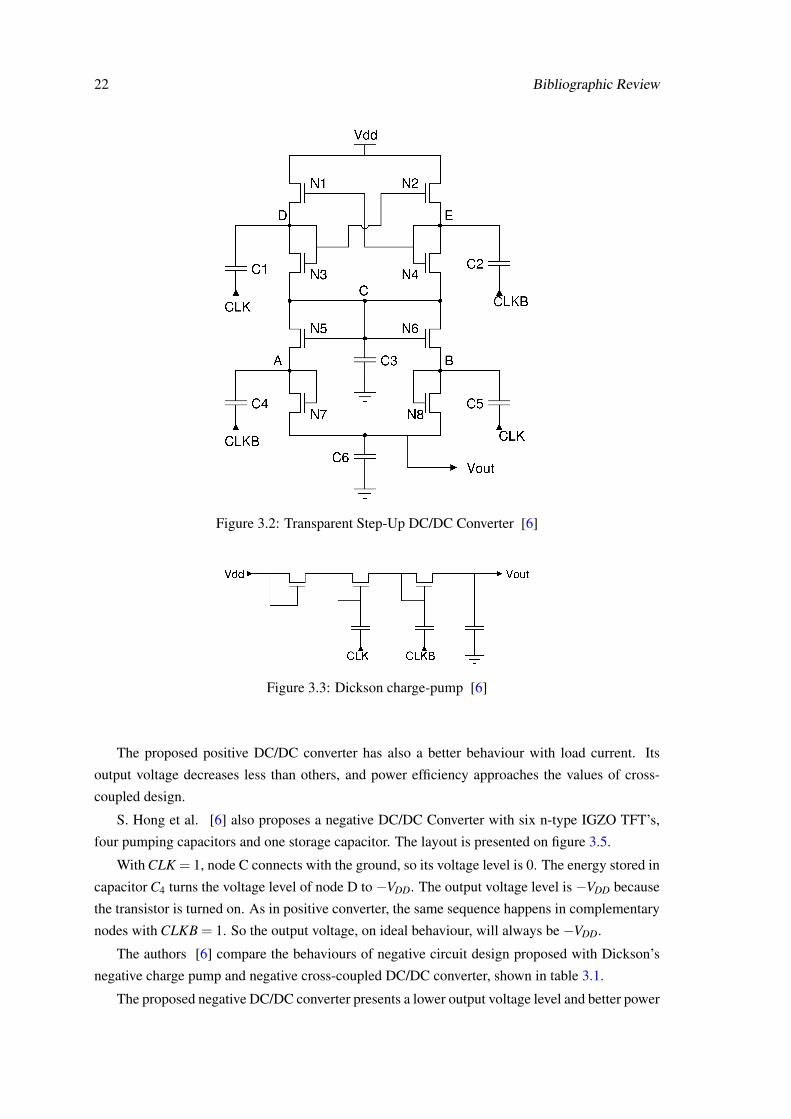
S. Hong et al. [6] present the most close device to what we need to achieved. The proposed
positive DC/DC Converter is presented in figure 3.2.
It has eight n-type IGZO TFT’s, four pumping capacitors and two storage capacitors. When
CLK = 1, the voltage level of node D is 2VDD because it receives the energy stored on capacitor C1.
Node C has a voltage level of 2VDD−Vth due to voltage drop across transistor N3. Therefore, node
B will receive the energy stored in capacitor C5, so its voltage level becomes 3VDD− 2Vth. With
the voltage drop in transistor N8, output voltage level is 3VDD−3Vth. The same sequence happens
in complementary nodes with CLKB = 1. As Vth << VDD, the output voltage level is higher than
the input voltage level.
The authors [6] compared the behaviour of positive circuit design proposed with Dickson’s
charge pump and positive cross-coupled DC/DC converter using n-type TFT’s, presented in figures
3.3 and 3.4.
With a supply voltage of 10 V and no load current, positive DC/DC converter presents an
output voltage level of 25 V. On other hand, Dickson’s charge pump presents 25.5 V and positive
cross-coupled DC/DC converter presents 19.5 V.
With a load current of 250µA, output voltage levels are 21.3 V, 20.4 V and 16.1 V respectively.
In this case, the power efficiencies measured are 69.5%, 58.4% and 77.3%. The values show that
Dickson’s charge pump has a good output voltage level, but its efficiency is much lower than the
other circuits. Cross-coupled DC/DC converter has good power efficiency, but its output voltage
level is lower than the others. The authors explain this fact with low driving capability of n-type
TFT’s on source follower structure during pull-up.
22 Bibliographic Review
Figure 3.2: Transparent Step-Up DC/DC Converter [6]
Figure 3.3: Dickson charge-pump [6]
The proposed positive DC/DC converter has also a better behaviour with load current. Its
output voltage decreases less than others, and power efficiency approaches the values of cross-
coupled design.
S. Hong et al. [6] also proposes a negative DC/DC Converter with six n-type IGZO TFT’s,
four pumping capacitors and one storage capacitor. The layout is presented on figure 3.5.
With CLK = 1, node C connects with the ground, so its voltage level is 0. The energy stored in
capacitor C4 turns the voltage level of node D to −VDD. The output voltage level is −VDD because
the transistor is turned on. As in positive converter, the same sequence happens in complementary
nodes with CLKB = 1. So the output voltage, on ideal behaviour, will always be −VDD.
The authors [6] compare the behaviours of negative circuit design proposed with Dickson’s
negative charge pump and negative cross-coupled DC/DC converter, shown in table 3.1.
The proposed negative DC/DC converter presents a lower output voltage level and better power
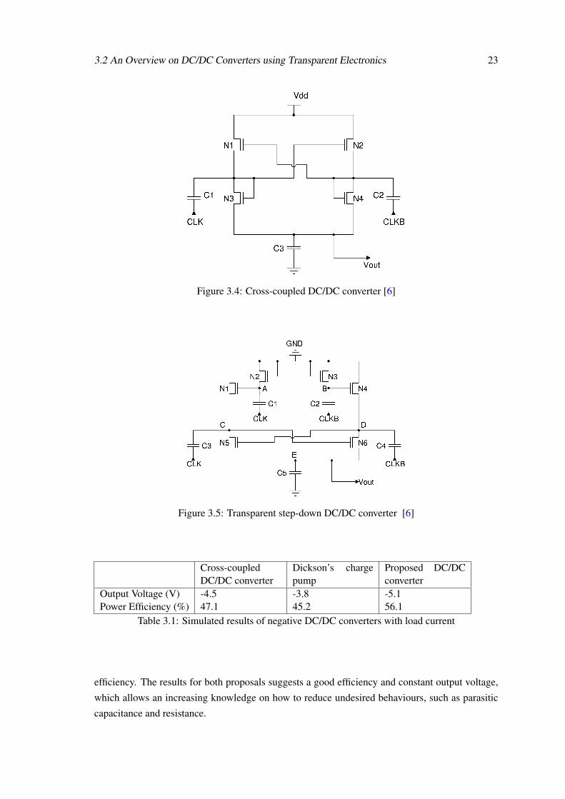
3.2 An Overview on DC/DC Converters using Transparent Electronics 23
Figure 3.4: Cross-coupled DC/DC converter [6]
Figure 3.5: Transparent step-down DC/DC converter [6]
Cross-coupledDC/DC converter
Dickson’s chargepump
Proposed DC/DCconverter
Output Voltage (V) -4.5 -3.8 -5.1Power Efficiency (%) 47.1 45.2 56.1
Table 3.1: Simulated results of negative DC/DC converters with load current
efficiency. The results for both proposals suggests a good efficiency and constant output voltage,
which allows an increasing knowledge on how to reduce undesired behaviours, such as parasitic
capacitance and resistance.
24 Bibliographic Review
3.2.3 DC/DC Converters in Organic Thin-Film Transistor Technology
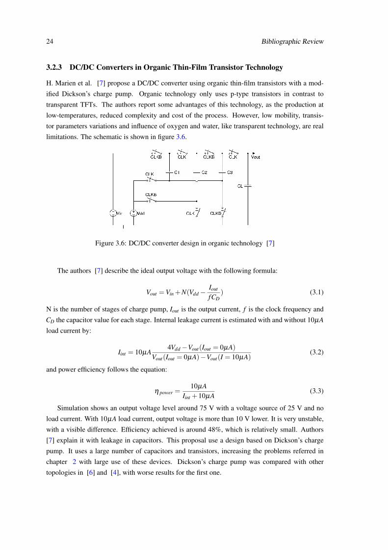
H. Marien et al. [7] propose a DC/DC converter using organic thin-film transistors with a mod-
ified Dickson’s charge pump. Organic technology only uses p-type transistors in contrast to
transparent TFTs. The authors report some advantages of this technology, as the production at
low-temperatures, reduced complexity and cost of the process. However, low mobility, transis-
tor parameters variations and influence of oxygen and water, like transparent technology, are real
limitations. The schematic is shown in figure 3.6.
Figure 3.6: DC/DC converter design in organic technology [7]
The authors [7] describe the ideal output voltage with the following formula:
Vout =Vin +N(Vdd−Iout
fCD) (3.1)
N is the number of stages of charge pump, Iout is the output current, f is the clock frequency and
CD the capacitor value for each stage. Internal leakage current is estimated with and without 10µA
load current by:
Iint = 10µA4Vdd−Vout(Iout = 0µA)
Vout(Iout = 0µA)−Vout(I = 10µA)(3.2)
and power efficiency follows the equation:
η power =10µA
Iint +10µA(3.3)
Simulation shows an output voltage level around 75 V with a voltage source of 25 V and no
load current. With 10µA load current, output voltage is more than 10 V lower. It is very unstable,
with a visible difference. Efficiency achieved is around 48%, which is relatively small. Authors
[7] explain it with leakage in capacitors. This proposal use a design based on Dickson’s charge
pump. It uses a large number of capacitors and transistors, increasing the problems referred in
chapter 2 with large use of these devices. Dickson’s charge pump was compared with other
topologies in [6] and [4], with worse results for the first one.
Chapter 4
Specifications
This chapter presents an initial proposal for DC/DC converter using transparent electronics, based
on switched-capacitors. Due to problems referred in chapter 2 with inductors, this suggestion only
uses the capacitors and TFTs. First section presents a boost converter. The second one presents a
buck converter.
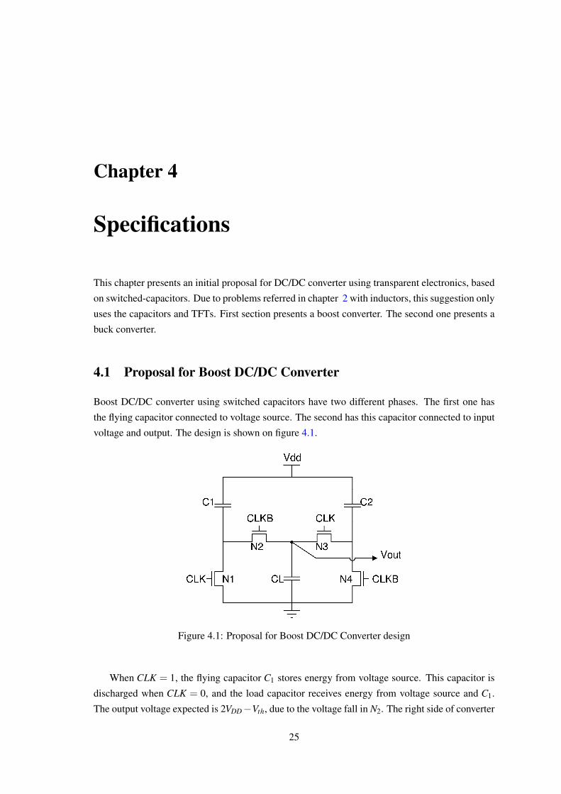
4.1 Proposal for Boost DC/DC Converter
Boost DC/DC converter using switched capacitors have two different phases. The first one has
the flying capacitor connected to voltage source. The second has this capacitor connected to input
voltage and output. The design is shown on figure 4.1.
Figure 4.1: Proposal for Boost DC/DC Converter design
When CLK = 1, the flying capacitor C1 stores energy from voltage source. This capacitor is
discharged when CLK = 0, and the load capacitor receives energy from voltage source and C1.
The output voltage expected is 2VDD−Vth, due to the voltage fall in N2. The right side of converter
25
26 Specifications
has the same behaviour as the left one with exchanged clock signals. This makes a more constant
output voltage level.
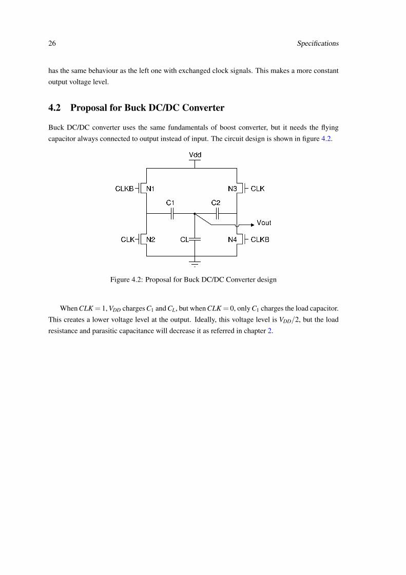
4.2 Proposal for Buck DC/DC Converter
Buck DC/DC converter uses the same fundamentals of boost converter, but it needs the flying
capacitor always connected to output instead of input. The circuit design is shown in figure 4.2.
Figure 4.2: Proposal for Buck DC/DC Converter design
When CLK = 1, VDD charges C1 and CL, but when CLK = 0, only C1 charges the load capacitor.
This creates a lower voltage level at the output. Ideally, this voltage level is VDD/2, but the load
resistance and parasitic capacitance will decrease it as referred in chapter 2.
Chapter 5
Conclusions and Future Work
This report contains the background necessary for the development of a DC/DC Converter with
transparent electronics and the bibliographic review with the state of the art on transparent con-
verters made so far. It was presented different device masks, the characteristics of TFT technology
and a study on voltage multipliers. During the remaining of the Master thesis, a physical imple-
mentation of the transparent DC/DC converter will be developed. The following tasks are to be
accomplished in order to complete the Master Thesis:
• Structural design of passive elements masks using CAD tools
• Proposal of a DC/DC Converter topology (possibly boost) with TFT’s and respective elec-
trical simulation
• Structural design of the masks for the converter and sending for fabrication
• Start writing the report
• Manufacturing and testing of developed circuits in CENIMAT-UNL
• Finishing writing the report
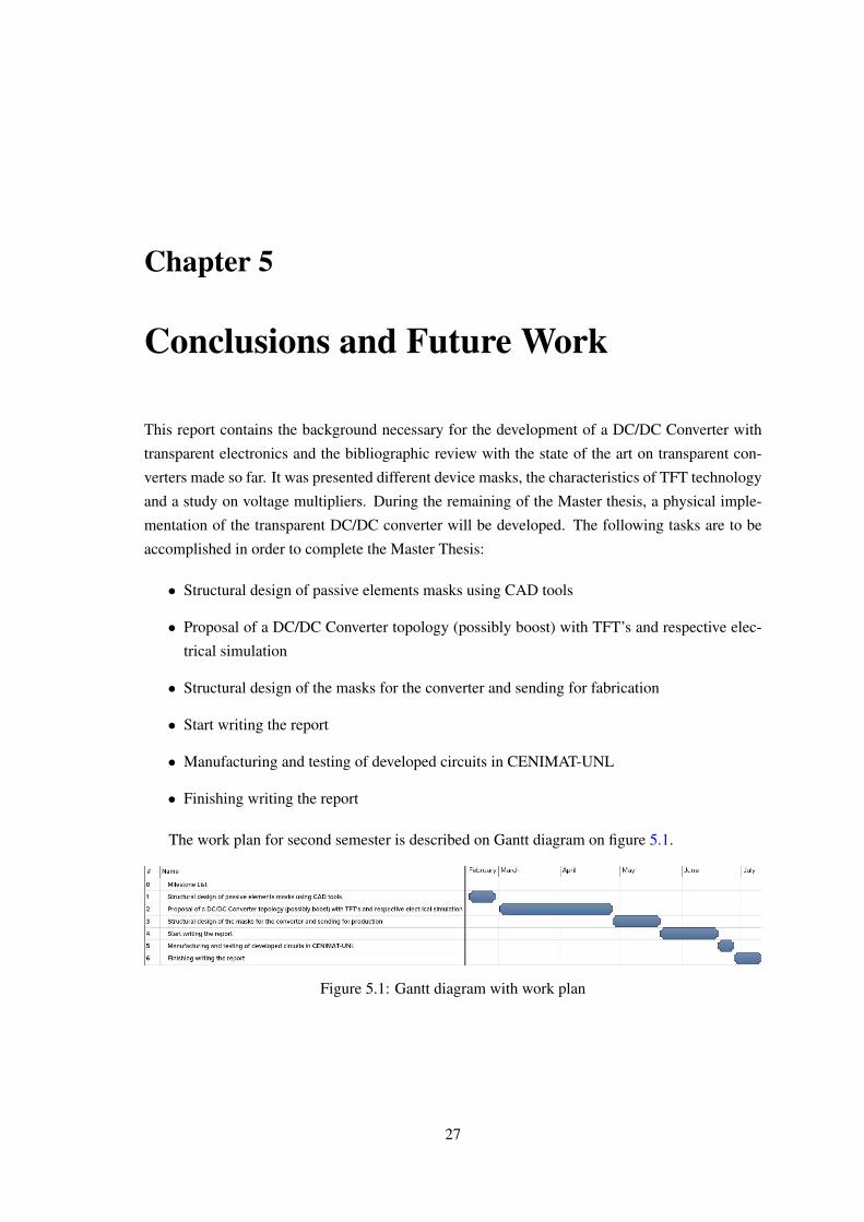
The work plan for second semester is described on Gantt diagram on figure 5.1.
Figure 5.1: Gantt diagram with work plan
27

28 Conclusions and Future Work
Bibliography
[1] M. Rashid. Power Electronics Handbook. Academic Press, 2001. ISBN 0-12-581650-2.
[2] Wager John F, Douglas A. Keszler, and Rick E. Presley. Transparent Electronics. Springer,2008. ISBN 978-0-387-72341-9.
[3] M. Wens and M. Steyaert. Design and Implementation of Fully-Integrated Inductive DC-DCConverters in Standard CMOS. Springer, 2011. ISBN 978-94-007-1435.
[4] J. Starzyk. A dc-dc charge pump design based on voltage doublers. IEEE Transactions onCircuits and Systems-I: Fundamental Theory and Applications, 48:350–358, 2001.
[5] B. Maity and P. Mandal. A switched-capacitor based embedded dc-dc buck converter forhigh power efficiency and high power density. TENCON - IEEE Region 10 Conference,pages 19–24, 2010.
[6] S. Hong et al. Dc-dc converters using indium gallium zinc oxide thin film transistors formobile display applications. Japanese Journal of Applied Physics, 49:03CB05, 2010.
[7] S. Steudel H. Marien, M. Steyaert and P. Vicca. An organic integrated capacitive dc-dcup-converter. Proccedings of the ESSCIRC, pages 510–513, 2010.
[8] R. L. Hoffman, B. J. Norris, and J. F. Wager. Zno-based transparent thin-film transistors.
[9] P. F. Carcia, R. S. McLean, M. H. Reilly, and G. Nunes Jr. Transparent zno thin-film transistorfabricated by rf magnetron sputtering. Applied Physics Letters, 82(7):1117–1119, 2003.
[10] S. Masuda, K. Kitamura, Y. Okumura, S. Miyatake, H. Tabata, and T. Kawai. Transpar-ent thin film transistors using zno as an active channel layer and their electrical properties.Journal of Applied Physics, 93(3):1624–1630, 2003.
[11] K. Nomura, H. Ohta, A. Takagi, T. Kamiya, M. Hirano, and H. Hosono. Room-temperaturefabrication of transparent flexible thin-film transistors using amorphous oxide semiconduc-tors. Nature, 432(7016):488–492, 2004.
[12] P. Barquinha, A. M. Vila, G. Gonçalves, L. Pereira, R. Martins, J. R. Morante, and E. For-tunato. Gallium-indium-zinc-oxide-based thin-film transistors: Influence of the source/drainmaterial. IEEE Transactions on Electron Devices, 55(4):954–960, 2008.
[13] A. Suresh and J. F. Muth. Bias stress stability of indium gallium zinc oxide channel basedtransparent thin film transistors. Applied Physics Letters, 92(3), 2008.
[14] M. E. Lopes, H. L. Gomes, M. C. R. Medeiros, P. Barquinha, L. Pereira, E. Fortunato,R. Martins, and I. Ferreira. Gate-bias stress in amorphous oxide semiconductors thin-filmtransistors. Applied Physics Letters, 95(6), 2009.
29
30 BIBLIOGRAPHY
[15] J. Jeong Y. Mo J. Jeong, H. Yang and H. Kim. Origin of threshold voltage instability inindium-gallium-zinc oxide thin film transistors. Applied Physics Letters, 93(123508):1–3,2008.
[16] S. Kuk et al. Light-induced hysteresis of in–ga–zn–o thin-film transistors with various tem-peratures. IEEE Electron Device Letters, 33:1279–1281, 2012.
[17] S. Lee et al. The effect of the photo-induced carriers on the reliability of oxide tfts undervarious intensities of light. IEEE Electron Device Letters, 33:218–220, 2012.
[18] P. Barquinha. Low-temperature sputtered mixtures of high-k and high bandgap dielectricsfor gizo tfts. Journal of the SID, 18(10):762–772, 2010.
[19] K. Nomura, T. Kamiya, M. Hirano, and H. Hosono. Origins of threshold voltage shifts inroom-temperature deposited and annealed a-in-ga-zn-o thin-film transistors. Applied PhysicsLetters, 95(1), 2009.
[20] A. Suresh, P. Wellenius, V. Baliga, H. Luo, L. Lunardi, and J. Muth. Fast-all transparentintegrated circuits based on indium gallium zinc oxide thin-film transistors. IEEE ElectronDevice Letters, 31(4):317–319, 2010.
[21] D. Kang, I. Kang, S. Ryu, and J. Jang. Self-aligned coplanar a-igzo tfts and application tohigh-speed circuits. IEEE Electron Device Letters, 32(10):1385–1387, 2011.