Embed Size (px)
Citation preview
DE2-115 Control
Panel - Part II
Digital Circuit Lab
TA: Po-Chen Wu
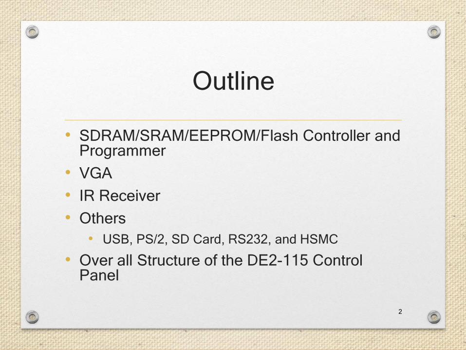
Outline
• SDRAM/SRAM/EEPROM/Flash Controller and Programmer
• VGA
• IR Receiver
• Others
• USB, PS/2, SD Card, RS232, and HSMC
• Over all Structure of the DE2-115 Control Panel
2
SDRAM/SRAM/EEPROM/
Flash Controller and
Programmer
3
Memory Controller and
Programmer
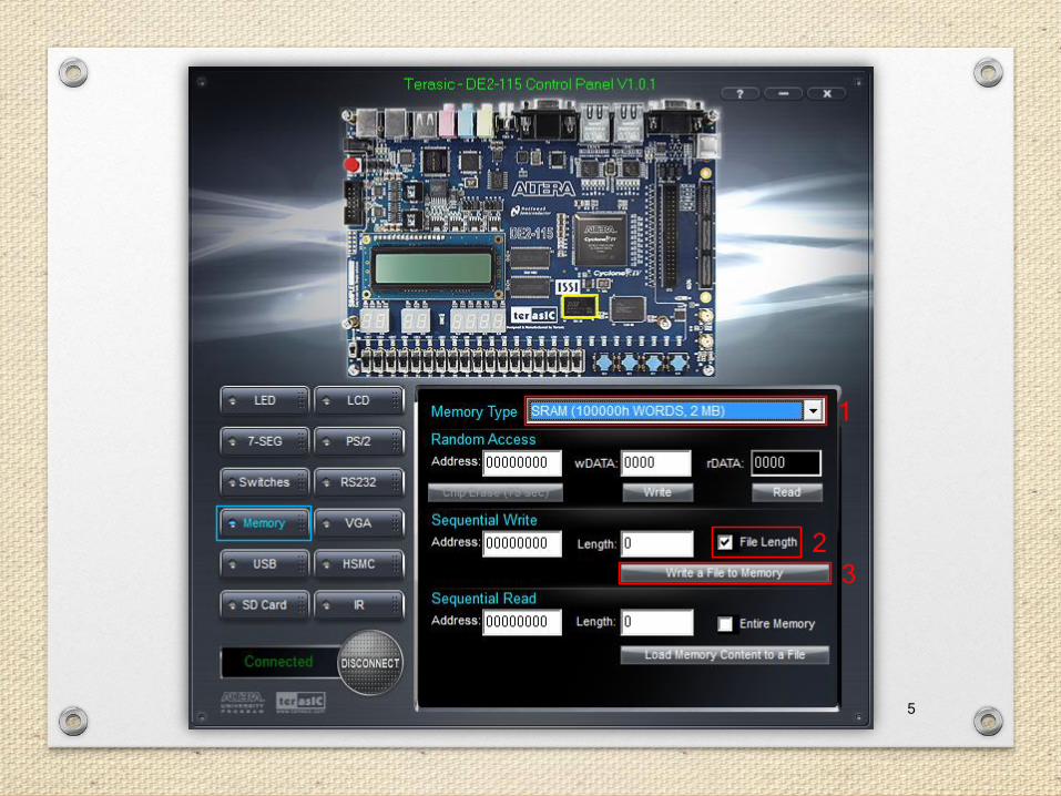
• The Control Panel can be used to write/read
data to/from the SRAM, SDRAM, EEPROM,
and Flash chips on the DE2-115 board.
• As an example, we will describe how the
SRAM may be accessed; the same approach
is used to access the SDRAM, EEPROM, and
Flash.
4
5
1
2
3
6
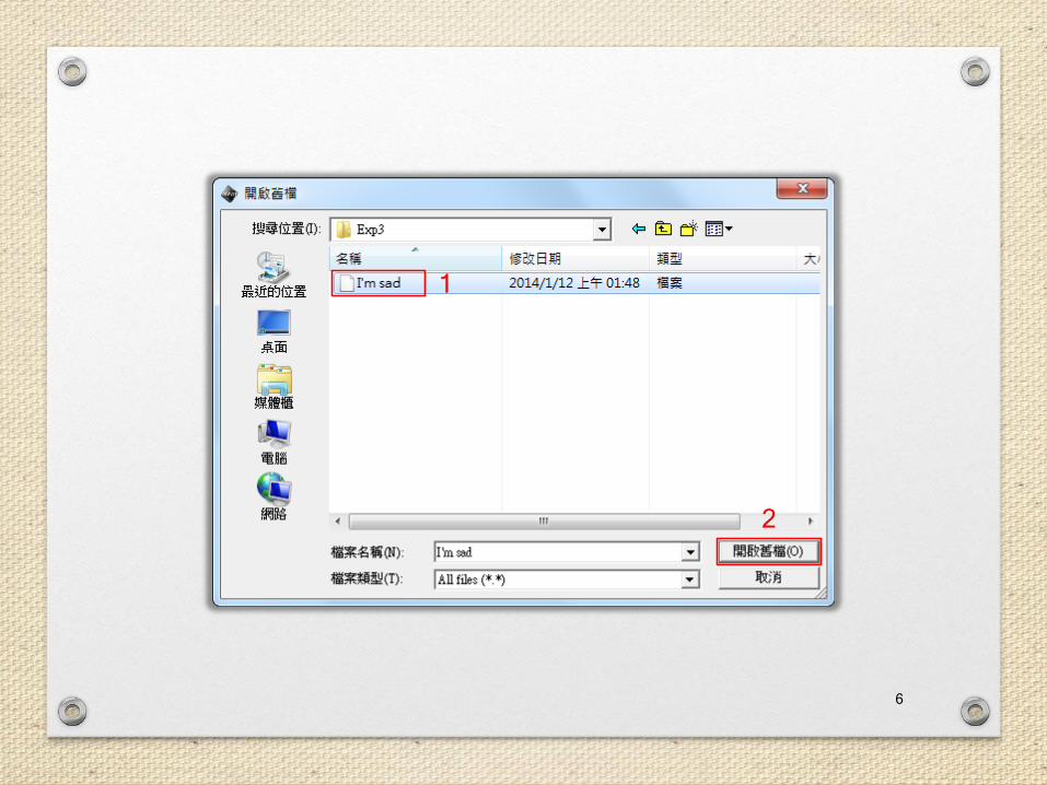
1
2
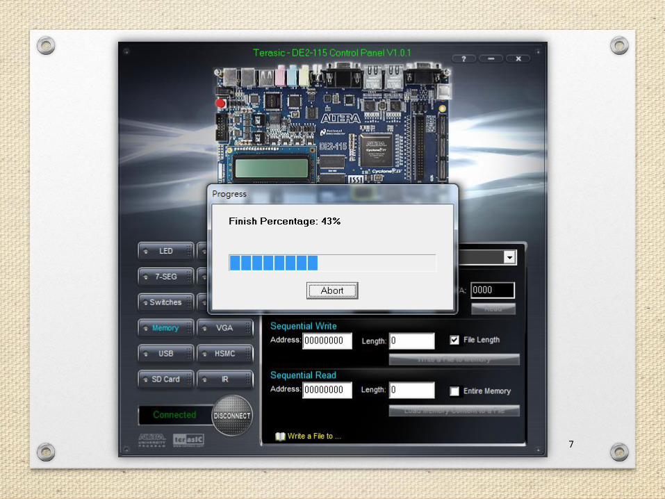
7
8
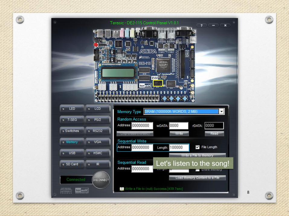
Let's listen to the song!
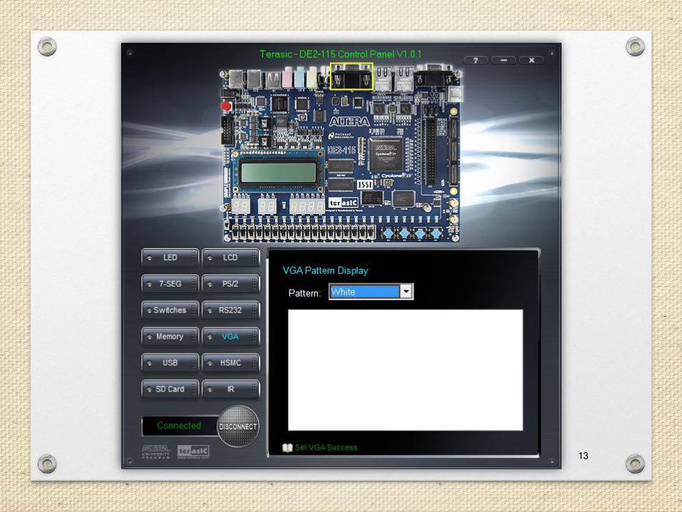
VGA
9
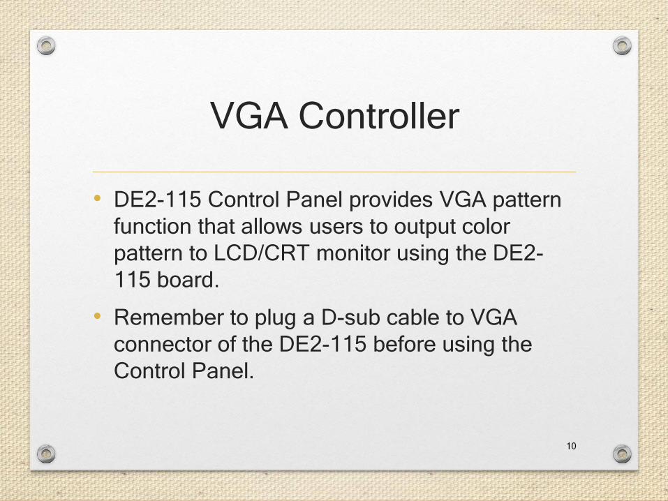
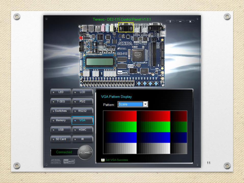
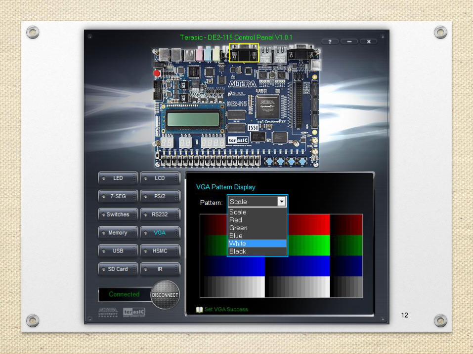
VGA Controller
• DE2-115 Control Panel provides VGA pattern
function that allows users to output color
pattern to LCD/CRT monitor using the DE2-
115 board.
• Remember to plug a D-sub cable to VGA
connector of the DE2-115 before using the
Control Panel.
10
11
12
13
IR Receiver
14
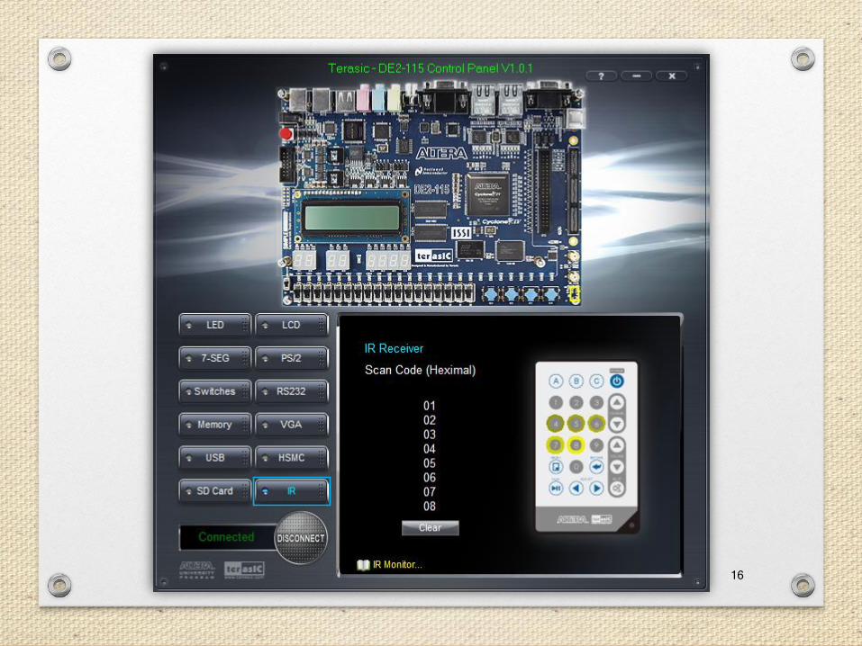
IR Receiver
• From the control panel, we can test the IR receiver on the DE2-115 by sending scan codefrom a remote controller.
• When the scan code is received, the information will be displayed on the Receiver window represented in hexadecimal.
• Also, the pressed button on the remote controller will be indicated on the graphic of remote controller on the IR receiver window.
15
16
Others
17
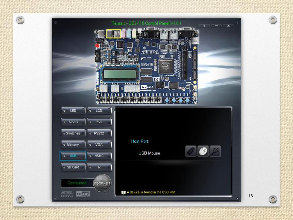
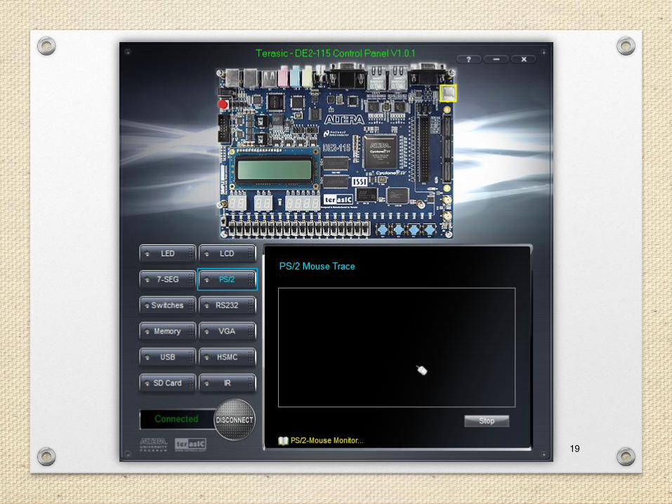
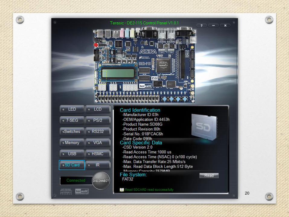
USB, PS/2, SD Card, RS232, and HSMC
18
19
20
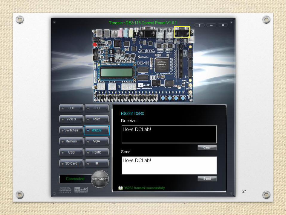
21
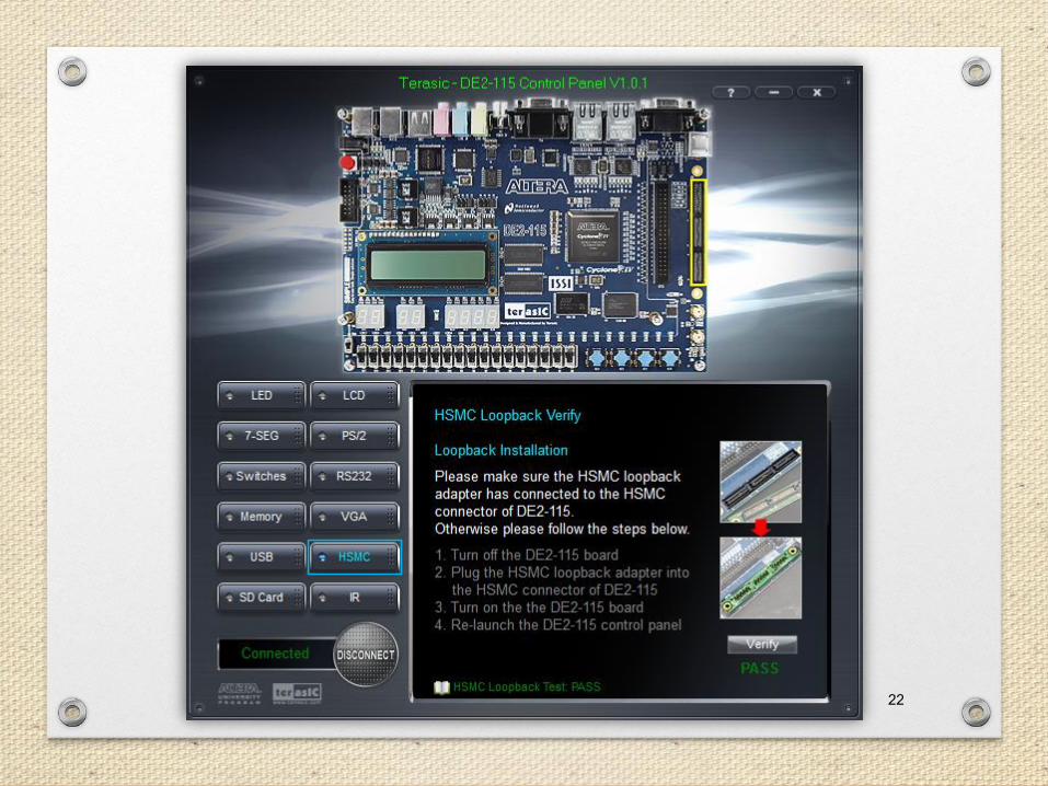
22
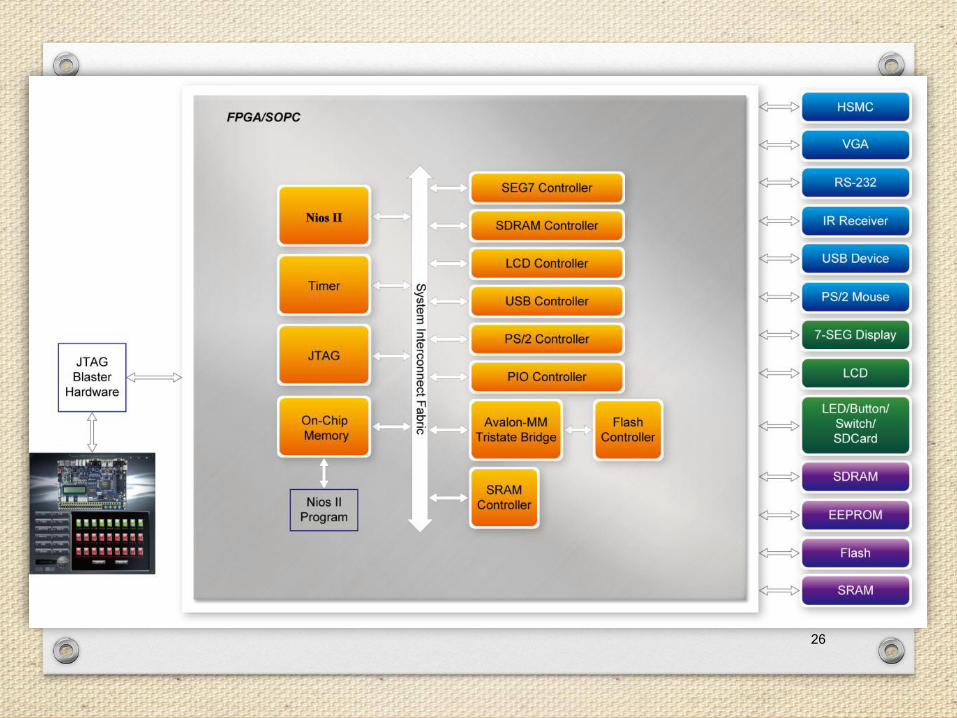
Over all Structure of the
DE2-115 Control Panel
23
Overall Structure (1/2)
• The DE2-115 Control Panel is based on a NiosII SOPC system instantiated in the Cyclone IV E FPGA with software running on the on-chip memory.
• The software part is implemented in C code; the hardware part is implemented in Verilog HDL code with SOPC builder.
• The source code is not available on the DE2_115 System CD.
24
Overall Structure (2/2)
• Each input/output device is controlled by the
Nios II Processor instantiated in the FPGA
chip.
• The communication with the PC is done via
the USB Blaster link.
• The Nios II interprets the commands set from
the PC and performs the corresponding
actions.
25
26

The End.
Any question?
Reference
1. "DE2-115 User Manual" by Terasic
Technologies Inc.
28