Embed Size (px)
Citation preview
Department of Biomedical Engineering
BME 317
Medical Electronics Lab
Modified by Dr.Husam AL.Hamad and Eng.Roba AL.Omari Summer 2009
2
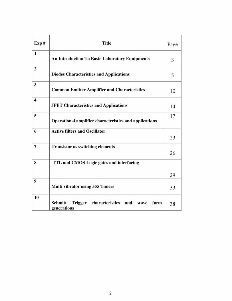
Exp #
Title
Page
1
An Introduction To Basic Laboratory Equipments
3
2
Diodes Characteristics and Applications
5
3
Common Emitter Amplifier and Characteristics
10
4
JFET Characteristics and Applications
14
5
Operational amplifier characteristics and applications 17
6 Active filters and Oscillator
23
7 Transistor as switching elements
26
8 TTL and CMOS Logic gates and interfacing
29 9
Multi vibrator using 555 Timers
33
10
Schmitt Trigger characteristics and wave form
generations
38
3
Experiment # 1
An Introduction to Basic Laboratory Equipment
Objective:
To become familiar with the available test and measurement equipment.
Measuring and Testing Equipment:
1. The Digital Multimeter (DMM).
It functions as an ohmmeter, Ammeter, and voltmeter. The ohmmeter measures
practically constant or variable resistance.
The ammeter measures the direct current or the rms value of the current by
connecting it in series with the circuit under test. At the time of connecting or
disconnecting of the ammeter to the certain circuit, the power supply should be
switched off.
The voltmeter measures the direct voltage or the rms value of voltage by
connecting it in parallel with the circuit under test.
2. The Oscilloscope (OSC).
It is basically a voltage sensing and display device. it cannot measure current directly.
The main functions of it are:
1. AC and DC measurements.
2. Phase shift Measurements.
3. Frequency measurements.
3. The Function Generator.(FG).
It provides voltages of different waveforms, output voltage frequency and amplitude
have a wide dynamic range. An adjustable level of DC offset is also available.
Practical Procedure:
4
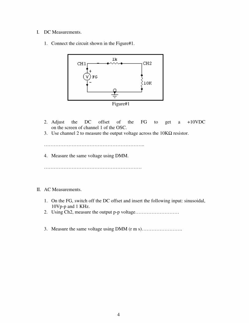
I. DC Measurements.
1. Connect the circuit shown in the Figure#1.
Figure#1
2. Adjust the DC offset of the FG to get a +10VDC
on the screen of channel 1 of the OSC.
3. Use channel 2 to measure the output voltage across the 10KΩ resistor.
……………………………………………………..
4. Measure the same voltage using DMM.
……………………………………………………
II. AC Measurements.
1. On the FG, switch off the DC offset and insert the following input: sinusoidal,
10Vp-p and 1 KHz.
2. Using Ch2, measure the output p-p voltage………………………
3. Measure the same voltage using DMM (r m s)…………………….
5
Experiment # 2
Diode Characteristics & Applications
Introduction:
When the diode anode is at a higher potential than the cathode, the diode is forward
biased, and current flows from anode to cathode. The diode is a nonlinear device with
a barrier potential (for Ge = 0.3 V, and for Si = 0.7 V). The Zener diode is used in
reverse biased as a simple voltage
Regulator.
Diode clippers are wave shaping circuits in that they are used to prevent signal
voltages from going above or below certain levels.
The clamper circuits add a dc level to the input waveform. Thus, the clamper is often
referred to as a dc restorer.
Half wave and full wave rectifier circuits cause AC input voltage to be converted into
a pulsed waveform having an average, or, DC, voltage output. A filter that consists of
an R-C circuit smoothes out the pulsating output voltage of the rectifier.
Objectives:
The purpose of this experiment is to investigate the diode characteristics and its
applications such as half wave rectifier, full wave rectifier, and voltage regulator
using Zener diode.
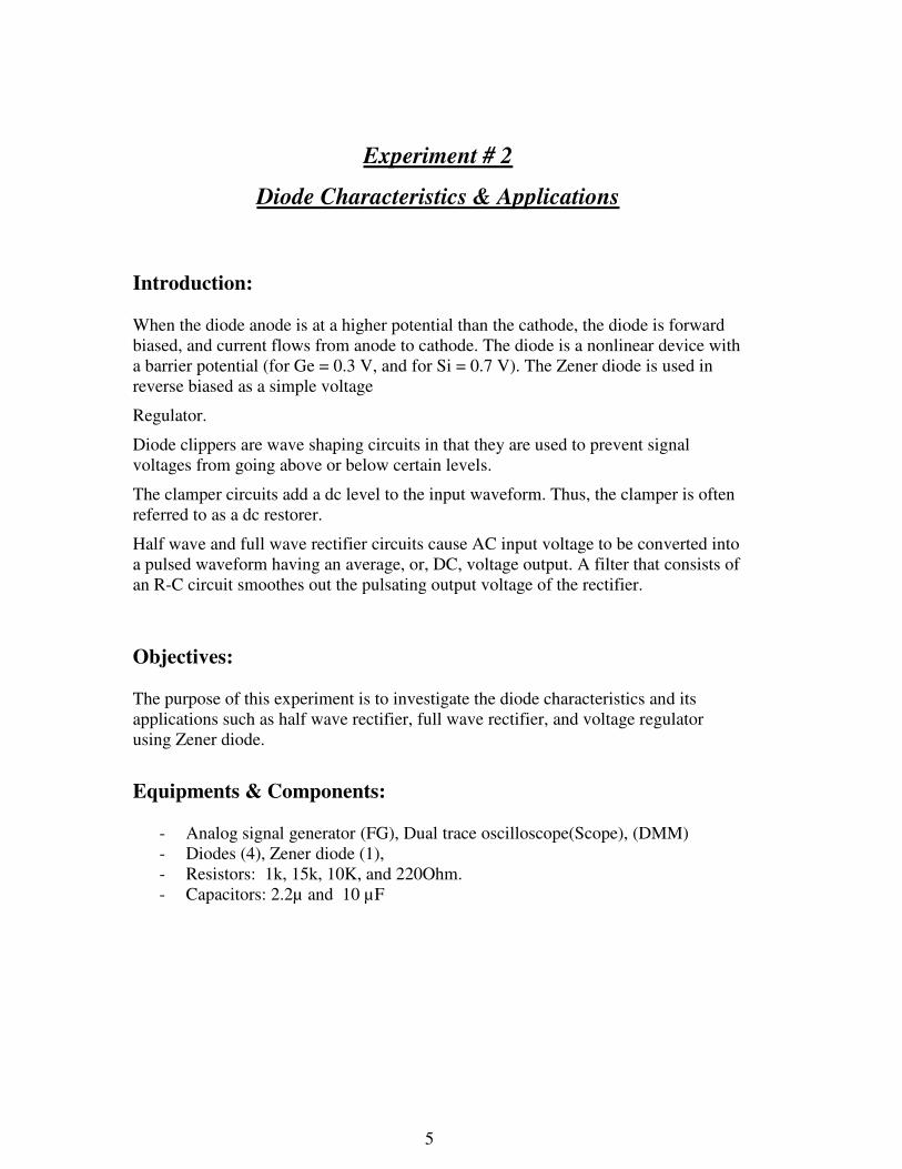
Equipments & Components:
- Analog signal generator (FG), Dual trace oscilloscope(Scope), (DMM)
- Diodes (4), Zener diode (1),
- Resistors: 1k, 15k, 10K, and 220Ohm.
- Capacitors: 2.2µ and 10 µF
6
3 4
+Vs
0-15
Vd
1k
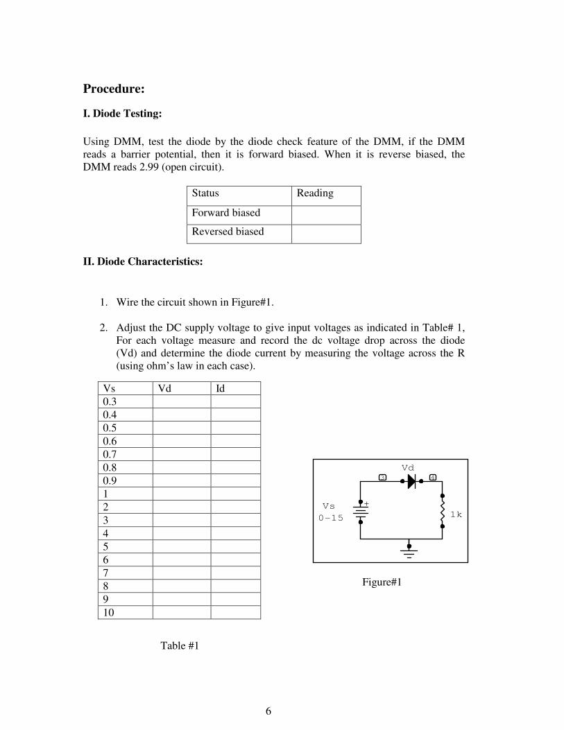
Procedure:
I. Diode Testing:
Using DMM, test the diode by the diode check feature of the DMM, if the DMM
reads a barrier potential, then it is forward biased. When it is reverse biased, the
DMM reads 2.99 (open circuit).
Status Reading
Forward biased
Reversed biased
II. Diode Characteristics:
1. Wire the circuit shown in Figure#1.
2. Adjust the DC supply voltage to give input voltages as indicated in Table# 1,
For each voltage measure and record the dc voltage drop across the diode
(Vd) and determine the diode current by measuring the voltage across the R
(using ohm’s law in each case).
Figure#1
Table #1
Vs Vd Id
0.3
0.4
0.5
0.6
0.7
0.8
0.9
1
2
3
4
5
6
7
8
9
10
7
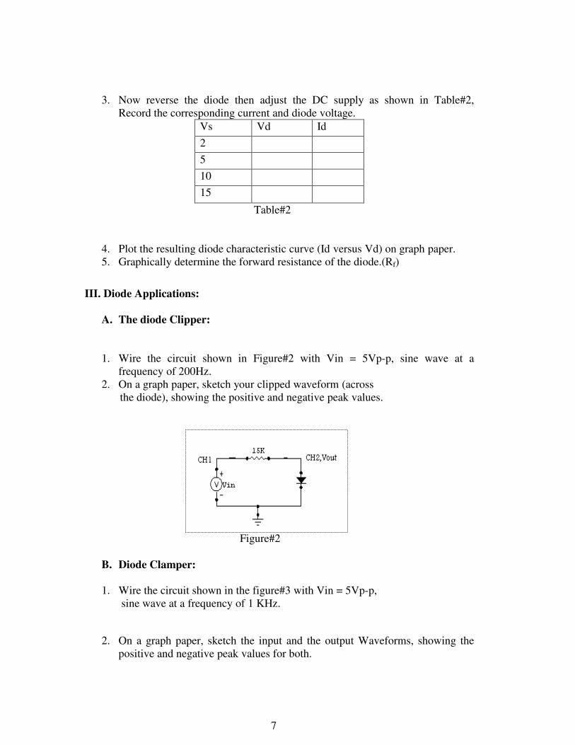
3. Now reverse the diode then adjust the DC supply as shown in Table#2,
Record the corresponding current and diode voltage.
Vs Vd Id
2
5
10
15
Table#2
4. Plot the resulting diode characteristic curve (Id versus Vd) on graph paper.
5. Graphically determine the forward resistance of the diode.(Rf)
III. Diode Applications:
A. The diode Clipper:
1. Wire the circuit shown in Figure#2 with Vin = 5Vp-p, sine wave at a
frequency of 200Hz.
2. On a graph paper, sketch your clipped waveform (across
the diode), showing the positive and negative peak values.
Figure#2
B. Diode Clamper:
1. Wire the circuit shown in the figure#3 with Vin = 5Vp-p,
sine wave at a frequency of 1 KHz.
2. On a graph paper, sketch the input and the output Waveforms, showing the
positive and negative peak values for both.
8
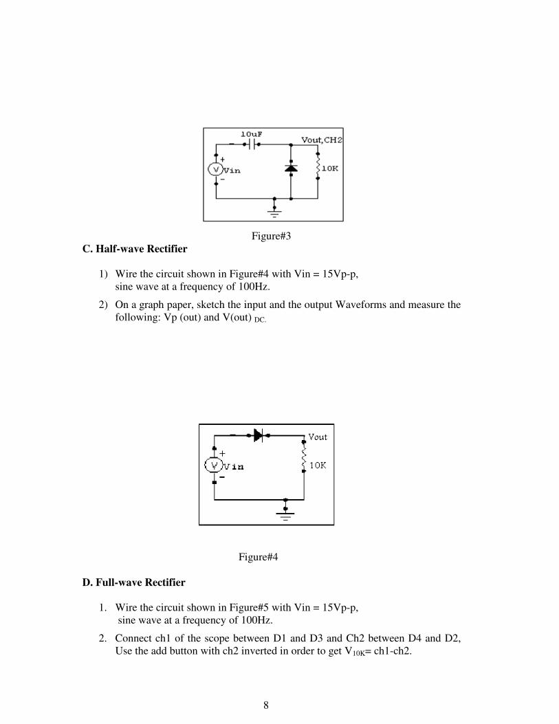
Figure#3
C. Half-wave Rectifier
1) Wire the circuit shown in Figure#4 with Vin = 15Vp-p,
sine wave at a frequency of 100Hz.
2) On a graph paper, sketch the input and the output Waveforms and measure the
following: Vp (out) and V(out) DC.
Figure#4
D. Full-wave Rectifier
1. Wire the circuit shown in Figure#5 with Vin = 15Vp-p,
sine wave at a frequency of 100Hz.
2. Connect ch1 of the scope between D1 and D3 and Ch2 between D4 and D2,
Use the add button with ch2 inverted in order to get V10K= ch1-ch2.

9
3. On a graph paper, sketch the output waveform and measure the following:
Vp(out) and VDC.
Figure#5
4. Filtering: Add a capacitor 2.2micro in parallel with 10K, sketch the output and
measure Vp(out), VDC(out), Vripple(p-p) and Vripple(rms)
E. Zener Diode Voltage Regulator:
1. Wire the circuit shown in figure#6 and measure:
a. Vout (FL): full load output voltage
b. Vout (NL): No-Load output voltage
Are they equal and why?
Figure#6
10
Experiment # 3
Common Emitter Characteristics
& Amplifier
Introduction:
The transistor bias method discussed in this experiment is the common emitter. The
common terminal is the one that is common to the input and the output in an ac
amplifier. The different bias configurations affect the various parameters of the ac
amplifier.
The transistor bias arrangement used most frequently is called the common emitter
configuration, in which the emitter terminal is grounded. In the common emitter
configuration the input current and voltage are IB and VBE respectively. The output
current and voltage are Ic and VCE. The ratio of collector current to base current is
called the current gain β:
Ib
Ic=β
The most important BJT small-signal configuration is the common emitter amplifier.
It is extremely useful because it has high voltage gain, high current gain, moderate
input resistance and moderate output resistance.
In many common emitter amplifiers, the emitter resistor is bypassed by connecting a
capacitor in parallel with it.
Objectives:
1. To construct input and output characteristics for the common emitter biasing
arrangement based on laboratory measurements.
2. To demonstrate the operation and characteristics of small- signal common
emitter amplifiers.
Equipments & Components:
• DMM, SCOPE, FG,
• 2N2222 silicon transistor or equivalent
11
• Resistors: l k Ω, 100 Ω, 56kΩ, 12kΩ, 3.3kΩ, and 2.2kΩ,
• Potentiometers: 1M Ω, and 10kΩ
• Capacitors: 47µF, and 2.2µF
Procedure:
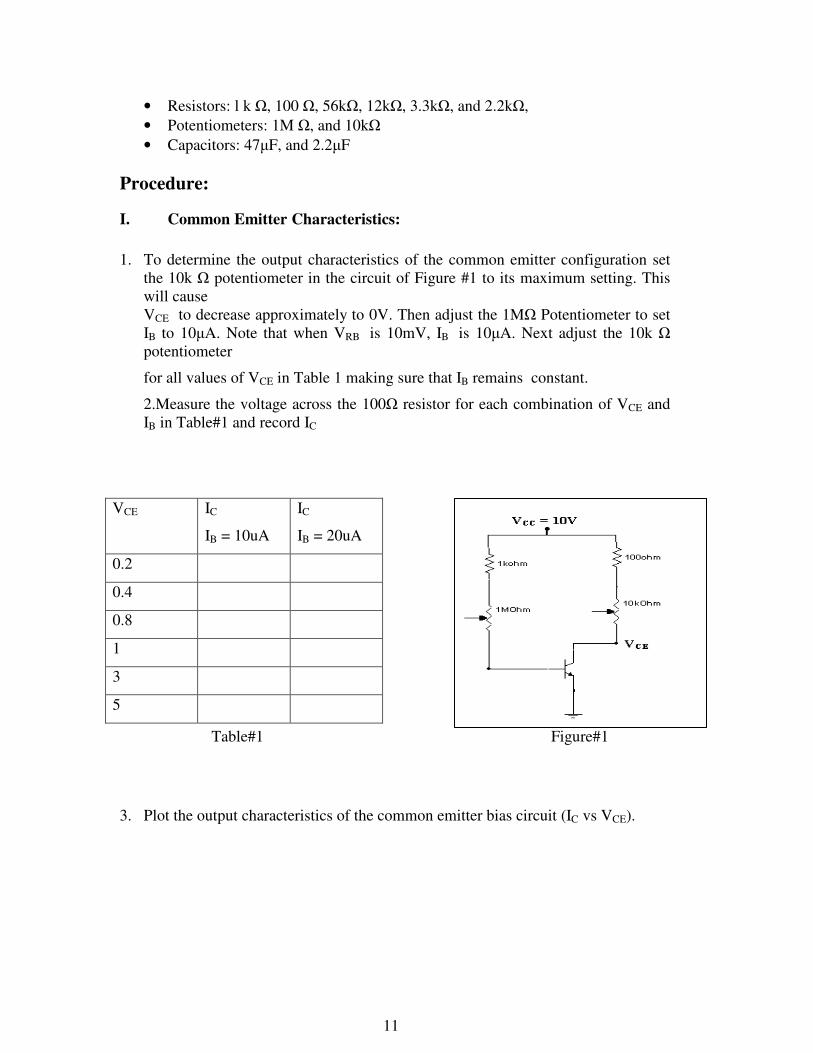
I. Common Emitter Characteristics:
1. To determine the output characteristics of the common emitter configuration set
the 10k Ω potentiometer in the circuit of Figure #1 to its maximum setting. This
will cause
VCE to decrease approximately to 0V. Then adjust the 1MΩ Potentiometer to set
IB to 10µA. Note that when VRB is 10mV, IB is 10µA. Next adjust the 10k Ω
potentiometer
for all values of VCE in Table 1 making sure that IB remains constant.
2.Measure the voltage across the 100Ω resistor for each combination of VCE and
IB in Table#1 and record IC
Table#1 Figure#1
3. Plot the output characteristics of the common emitter bias circuit (IC vs VCE).
VCE IC
IB = 10uA
IC
IB = 20uA
0.2
0.4
0.8
1
3
5
12
II. Common Emitter Amplifier:
DC Analysis
1. Wire the circuit shown in Figure #2 (omitting the FG) and measure the DC
parameters of the amplifier: VB, VC, VE, VCEQ and ICQ. Recording your results in
Table#2.
Table #2 Figure #2
AC Analysis
1. Connect the FG as shown in Figure # 2 and adjust the sine wave output level
of the FG at 200mVp-p and a frequency of I0kHz. Measure and record the
peak-to-peak output voltage Vo for the following conditions:
# Condition Vs Vo Measured
Gain
Expected Gain
1 Normal circuit
(Figure #2)
200mVp-p
reRE
RC
+1
2 With R Load
=2.2K(connected
between Vout and
ground)
200mvp-p
reRE
RLRC
+1
//
Parameter Measured values
VB
VC
VE
VCEQ
IEQ
VTre =
13
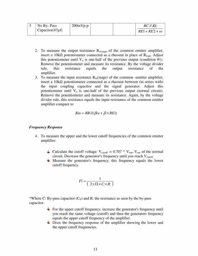
3 No By- Pass
Capacitor(47µf)
200mVp-p
reRERE
RLRC
++ 21
//
2. To measure the output resistance Ro(stage) of the common emitter amplifier,
insert a 10kΩ potentiometer connected as a rheostat in place of Rload. Adjust
this potentiometer until Vo is one-half of the previous output (condition #1).
Remove the potentiometer and measure its resistance. By the voltage divider
rule, this resistance equals the output resistance of the
amplifier.
3. To measure the input resistance Rin(stage) of the common -emitter amplifier,
insert a 10kΩ potentiometer connected as a rheostat between (in series with)
the input coupling capacitor and the signal generator. Adjust this
potentiometer until Vo is one-half of the previous output (normal circuit).
Remove the potentiometer and measure its resistance. Again, by the voltage
divider rule, this resistance equals the input resistance of the common emitter
amplifier compare to
)1//( REreRBRin ×+= ββ
Frequency Response
4. To measure the upper and the lower cutoff frequencies of the common emitter
amplifier:
Calculate the cutoff voltage: Vcutoff = 0.707 * Vout, Vout of the normal
circuit, Decrease the generator's frequency until you reach Vcutoff.
Measure the generator's frequency; this frequency equals the lower
cutoff frequency.
( )RCFl
××Π×=
2
1
*Where C: By-pass capacitor (CE) and R: the resistance as seen by the by-pass
capacitor.
For the upper cutoff frequency, increase the generator's frequency until
you reach the same voltage (cutoff) and then the generators frequency
equals the upper cutoff frequency of the amplifier.
Draw the frequency response of the amplifier showing the lower and
the upper cutoff frequencies.
14
Experiment # 4
sJFET Characteristics and Application
Objectives:
1. To demonstrate the characteristics of junction field effect transistors.
2. To demonstrate the operation and characteristics of small-signal common source
amplifier (CS).
Equipments & Components:
• DMM, SCOPE, FG and DC supply.
• N-channel JFET transistor 2N5457
• Resistors: 0.1 KΩ, 1 KΩ, 1.8 KΩ and 100 KΩ.
• Capacitors: 2.2 µF, and 47 µF.
• 10 KΩ Potentiometer.
• Diode.
Procedure:
I-Common source Characteristics:
1. Connect the circuit shown below in Fig.1.
2. Put VGS =0 this value must be constant during this step, then vary E2 to vary
VDS ,as recorded in Table #1, and measure the corresponding ID.
Figure#1
15
)(
2
offVGS
IDssgmo
×=
Table#1
3. Repeat step 2 for VGS = -1, then Plot the common source characteristic curve (ID
vs VDS).
II- Transfer Characteristics:
1. Wire the circuit shown in Figure #2, in this part the scope is set up to function as
an X-Y plotter, adjust the frequency of the FG to 500Hz and at a signal level
sufficient to produce a display similar to the transfer characteristics of the JFET.
2. Estimate from the scope's display both IDss and VGS(Off).
3. Calculate the JFET forward transconductance at VGS=0, (gmo).
Figure #2
III- Common Source Amplifier:
1. Wire the circuit shown in Figure#3 omitting the function generator, then
measure IDQ, VGSQ and gm. let VDD = 15V.
VDS
(V) 0 0.3 0.5 1 2 3 5 7 12
ID
(mA)
16
Vs
100kohm
1.8kohm
1kohm
2.2uF
2.2uF
47uF
VDD
Vo
RL1kohm
Figure #3
2. Connect the function generator as shown in Figure #3, and adjust the sine wave
output level of the function generator at 0.3 Vp-p and a frequency of 5 KHz.
3. On a graph paper, sketch the input and output voltages. Note the phase shift
between the input and output signals.
4. Measure the voltage gain for the cases in Table #2.
Table #2
4. Measure Ri and Ro for Condition #2, use 1MΩ potentiometer for Rin, why?
5. Measure the lower and the upper cutoff frequencies for Condition #2.
# Condition Vs Vo Measured
Gain
Expected Gain
1 Normal
Circuit(Fig#3)
300mVp-p ( )RDRLgm //×
2 No Load 300mVp-p ( )RDgm ×
3 No By-Pass
Capacitor
300mVp-p ( )( )Rsgm
RDgm
×+
×
1
17
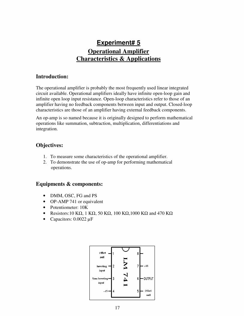
Experiment# 5
Operational Amplifier
Characteristics & Applications
Introduction:
The operational amplifier is probably the most frequently used linear integrated
circuit available. Operational amplifiers ideally have infinite open-loop gain and
infinite open loop input resistance. Open-loop characteristics refer to those of an
amplifier having no feedback components between input and output. Closed-loop
characteristics are those of an amplifier having external feedback components.
An op-amp is so named because it is originally designed to perform mathematical
operations like summation, subtraction, multiplication, differentiations and
integration.
Objectives:
1. To measure some characteristics of the operational amplifier.
2. To demonstrate the use of op-amp for performing mathematical
operations.
Equipments & components:
• DMM, OSC, FG and PS
• OP-AMP 741 or equivalent
• Potentiometer: 10K
• Resistors:10 KΩ, 1 KΩ, 50 KΩ, 100 KΩ,1000 KΩ and 470 KΩ
• Capacitors: 0.0022 µF
18
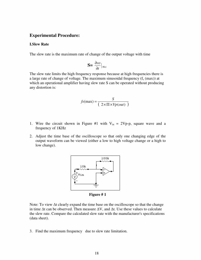
Experimental Procedure:
I.Slew Rate
The slew rate is the maximum rate of change of the output voltage with time
S= Maxt
vo
∂
∂
The slew rate limits the high frequency response because at high frequencies there is
a large rate of change of voltage. The maximum sinusoidal frequency (fs (max)) at
which an operational amplifier having slew rate S can be operated without producing
any distortion is:
1. Wire the circuit shown in Figure #1 with Vin = 2Vp-p, square wave and a
frequency of 1KHz 2. Adjust the time base of the oscilloscope so that only one changing edge of the
output waveform can be viewed (either a low to high voltage change or a high to
low change).
Figure # 1
Note: To view ∆t clearly expand the time base on the oscilloscope so that the change
in time ∆t can be observed. Then measure ∆V, and ∆t. Use these values to calculate
the slew rate. Compare the calculated slew rate with the manufacturer's specifications
(data sheet).
3. Find the maximum frequency due to slew rate limitation.
( ))(2(max)
outVp
Sfs
×Π×=
19
1M
1M
4. Change Vin to a 20 Vp-p, 1 KHz sinusoidal signal. Let Rf be 10 KΩ. Increase the
frequency beyond the calculated maximum frequency. Note the changes in the
output signal.
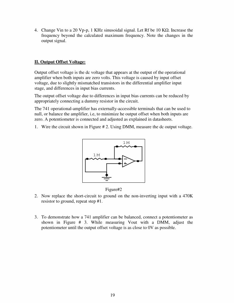
II. Output Offset Voltage:
Output offset voltage is the dc voltage that appears at the output of the operational
amplifier when both inputs are zero volts. This voltage is caused by input offset
voltage, due to slightly mismatched transistors in the differential amplifier input
stage, and differences in input bias currents.
The output offset voltage due to differences in input bias currents can be reduced by
appropriately connecting a dummy resistor in the circuit.
The 741 operational-amplifier has externally-accessible terminals that can be used to
null, or balance the amplifier, i.e, to minimize he output offset when both inputs are
zero. A potentiometer is connected and adjusted as explained in datasheets.
1. Wire the circuit shown in Figure # 2. Using DMM, measure the dc output voltage.
Figure#2
2. Now replace the short-circuit to ground on the non-inverting input with a 470K
resistor to ground, repeat step #1.
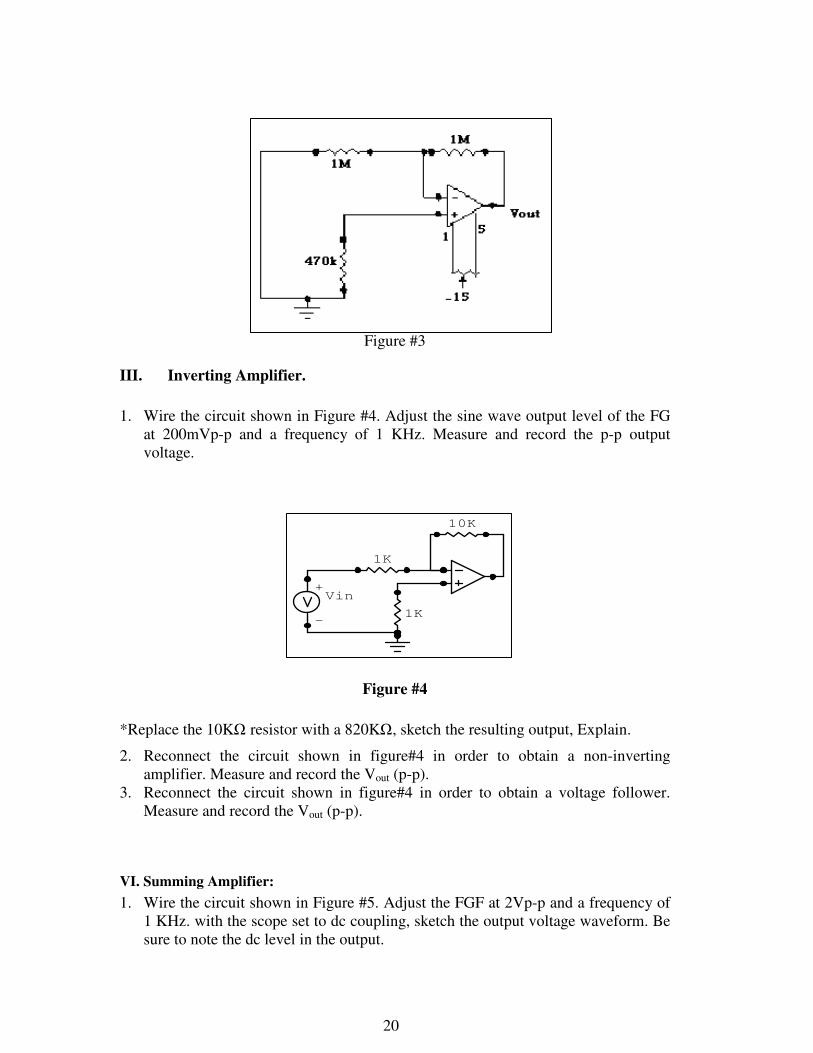
3. To demonstrate how a 741 amplifier can be balanced, connect a potentiometer as
shown in Figure # 3. While measuring Vout with a DMM, adjust the
potentiometer until the output offset voltage is as close to 0V as possible.
20
1K
+
-
Vin
10K
1K
Figure #3
III. Inverting Amplifier.
1. Wire the circuit shown in Figure #4. Adjust the sine wave output level of the FG
at 200mVp-p and a frequency of 1 KHz. Measure and record the p-p output
voltage.
Figure #4
*Replace the 10KΩ resistor with a 820KΩ, sketch the resulting output, Explain.
2. Reconnect the circuit shown in figure#4 in order to obtain a non-inverting
amplifier. Measure and record the Vout (p-p).
3. Reconnect the circuit shown in figure#4 in order to obtain a voltage follower.
Measure and record the Vout (p-p).
VI. Summing Amplifier:
1. Wire the circuit shown in Figure #5. Adjust the FGF at 2Vp-p and a frequency of
1 KHz. with the scope set to dc coupling, sketch the output voltage waveform. Be
sure to note the dc level in the output.
21
RC
C1
+
-
Vin
R1 Rf
Figure #5
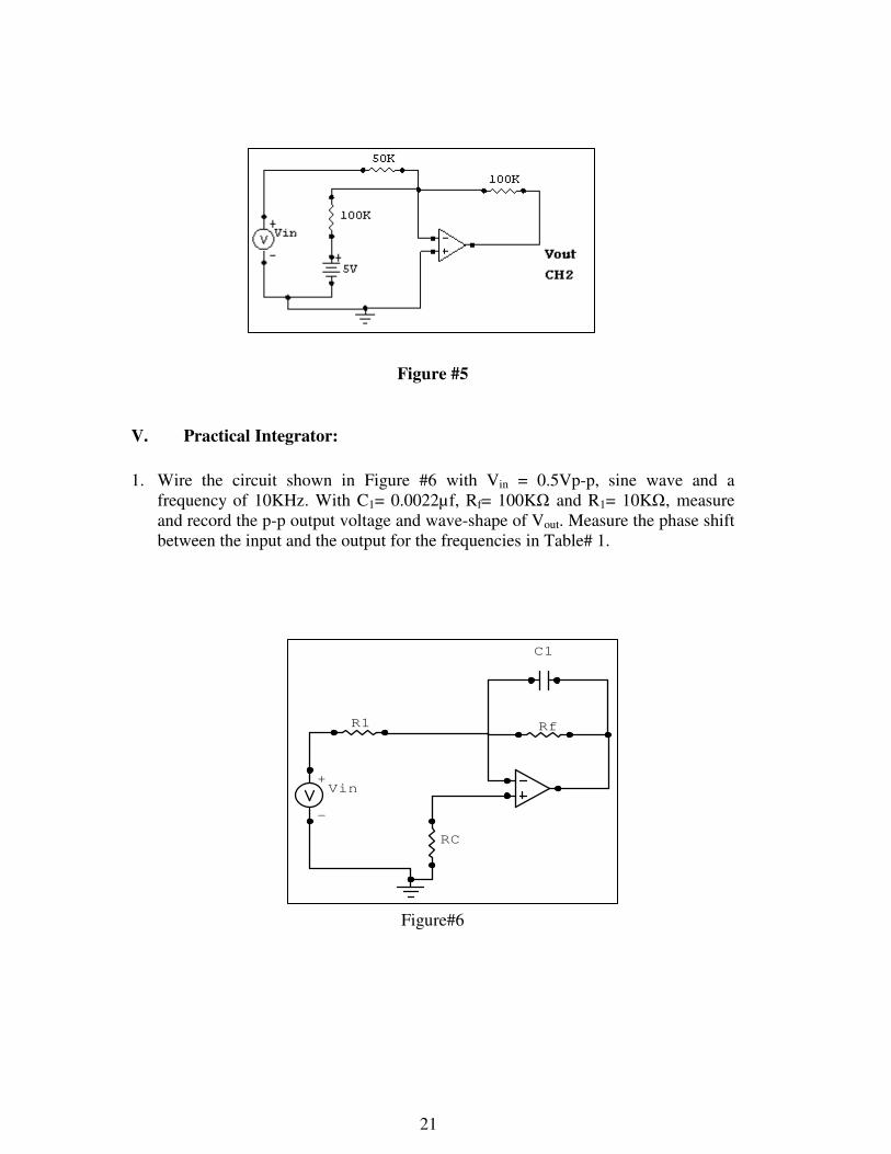
V. Practical Integrator:
1. Wire the circuit shown in Figure #6 with Vin = 0.5Vp-p, sine wave and a
frequency of 10KHz. With C1= 0.0022µf, Rf= 100KΩ and R1= 10KΩ, measure
and record the p-p output voltage and wave-shape of Vout. Measure the phase shift
between the input and the output for the frequencies in Table# 1.
Figure#6
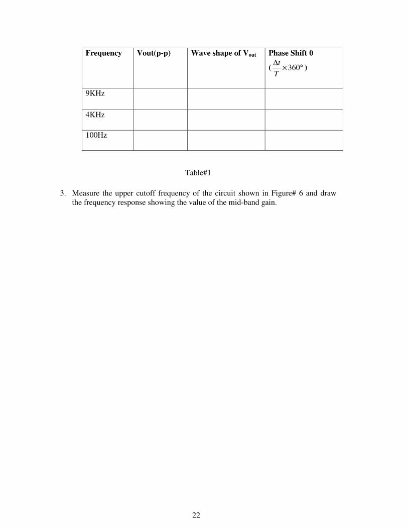
22
Frequency Vout(p-p) Wave shape of Vout Phase Shift θ
( °×∆
360T
t)
9KHz
4KHz
100Hz
Table#1
3. Measure the upper cutoff frequency of the circuit shown in Figure# 6 and draw
the frequency response showing the value of the mid-band gain.

23
6Experiment#
ve Filters & OscillatorsActi
Introduction:
I. Filters:
Active filters usually use IC operational amplifiers to provide gain and impedance
matching, together with passive RC circuit to provide the desired frequency response.
Filters are named after their frequency response characteristics: low-pass, high-pass,
band-pass and band-stop filters.
A low-pass filter passes low frequencies and attenuates high frequencies, a band-pass
filter allows a range (band) of frequencies to pass while attenuating frequencies
outside the band on either side.
The frequency at which the output voltage equals 0.707 times the input voltage is
referred to as the high or low frequency roll-off point. This point is also defined as the
frequency at which the output voltage has dropped by 3 dB.
Each kind of filter's response can be customized slightly by changing circuit
components to achieve certain characteristics that are useful in electronic
applications.
A filter is said to have a Butterworth, Chebyshev, or Bessel characteristics. The
choice of characteristic is based on the application and factor such as the need for a
linear phase shift with frequency (Bessel), or maximum roll-off of some what over -
20dB/decade (Chebyshev), or a maximally flat response in the pass band (Butter
worth).
II. Oscillators:
In feedback amplifier if the loop gain = 1 the amplifier will become critical stable.
This will occur at a single frequency fr, in other words the closed loop gain of the
amplifier will become infinite at only one frequency fr .Physically this means that an
output is possible with no input.
*Loop Gain= closed- loop gain × Feed- back ratio
The Wien bridge oscillator is an example of low frequency oscillators and it's used to
generate sinusoidal signals at frequencies ranging from 5Hz to 1MHz.
24
Objectives:
1. To demonstrate the operation and characteristics of the low and high
pass active filters.
2. To demonstrate the operation of Wien bridge oscillators
Equipments and components:
• DMM, Scope, FG, PS
• OP-AMP 741 or equivalent
• Resistors: 47k, 27k, 10k, 6.8k, 1.5k, and 1k Ω.
• Capacitors: 0.033 µF, 0.0047 µF, 0.1 µF, and 0.47 µF
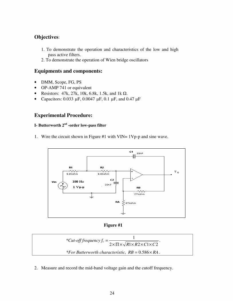
Experimental Procedure:
I- Butterworth 2nd
-order low-pass filter
1. Wire the circuit shown in Figure #1 with VIN= 1Vp-p and sine wave.
Figure #1
*Cut-off frequency fc =21212
1
CCRR ××××Π×.
*For Butterworth characteristic, RARB ×= 586.0 .
2. Measure and record the mid-band voltage gain and the cutoff frequency.

25
II- Wien bridge oscillator
1. Wire the circuit shown in Figure #2. With R1=R2=R=10 kΩ and C1=
C2=C=0.1µF
Figure#2
2. Carefully adjust the 1kΩ potentiometer until the output waveform has the least
amount of distortion. Measure the amplitude and the frequency of this signal.
( )CRfr
××Π×=
2
1
3. Replace C1 and C2 with 0.47µF. Repeat step 2.
26
Experiment# 7
Transistors as a Switching Elements (Inverters)
Introduction: The transistors can operate as switching elements when proper acting signals are
used. When used as a switch, the transistor operates in either the on region or in the
off region.
When the bipolar junction transistor (BJT) is used as a switch, it's operated in
saturation region to simulate the on (closed) switch condition and in the cut-off region
to simulate the off (open) switch condition. On state:
When the base emitter junction is forward-biased and there is enough base current to
produce a maximum current (IC(sat)) the transistor is in saturated and VCE is
approximately zero(the resistance between the collector and the emitter is very low
(typically 1Ω to 50Ω)).
IC (sat) = Vcc \ Rc
Off state:
When the base emitter junction is reverse-biased, all of the currents are approximately
zero and VCE(off) = VCC.(the resistance between the collector and the emitter is very
high (typically 10MΩ)).
Transistor Switching Time:
Because of junction capacitance and charge storage, the transistor don't switch on or
off in zero time.
Assume initially that the transistor is being hold off by Vin(low), so no collector current
flows and Vo=VCC. In this situation both transistor junctions are reverse-biased. The
Emitter-Base Junction (EBJ) will be reverse biased by Vin(low) . Thus the EBJ
27
capacitance is charged up to Vin(low) and the CBJ capacitance is charged up to
(Vin(low)+VCC ).
When the Vin rises from Vin(low) to Vin(high) , the collector current doesn't respond
immediately. Rather a delay time elapses before collector current begins to flow. This
delay time is required mainly for the EBJ capacitance to charge up to VBE
(approximately=0.7V).
Objectives:
1. To demonstrate the characteristics of Bipolar transistors as a
switching elements.
2. To demonstrate methods for speeding up the switching times of BJT switch.
3. To demonstrate resistance transistor logic (RTL) NOT and NOR
gates.
Equipments & components:
- OSC, FG, PS, DMM.
- Transistors BJT npn.
- Resistors: 100 KΩ, 22 KΩ, 4.7 KΩ, 2.2KΩ, 1 KΩ, 0.5 KΩ, and 0.1 KΩ.
- Capacitor: 1 µF, 0.1 µF, and 0.01 µF.
Procedure:
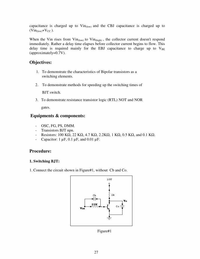
1. Switching BJT:
1. Connect the circuit shown in Figure#1, without Cb and Co.
Figure#1
28
2. Verify the truth table of the inverter.( as indicated)
Vin (volt) Vout
0
10
3. Set VIN=10Vp-p triangular wave with 1KHz frequency, set the scope in the
X-Y position, DC coupling. Sketch the transfer characteristics for the
inverter.
4. Add Co=0.1 µf then set VIN=4Vp-p square wave with f =1 KHz. Sketch Vin
and Vo. Increase and decrease the input frequency then note its effect on tr
and tf .(rise and falling times) .
5. For table#1. Measure the rise time (tr) and (tf ) for Vo according to table #1 .
Table #1
6. Connect 1 µf capacitor in parallel with RB. Measure the rise and fall times.
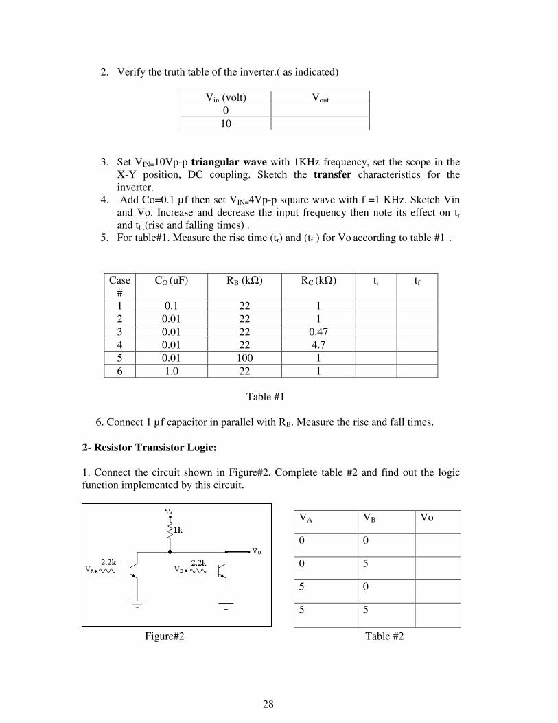
2- Resistor Transistor Logic:
1. Connect the circuit shown in Figure#2, Complete table #2 and find out the logic
function implemented by this circuit.
Figure#2 Table #2
Case
#
CO (uF) RB (kΩ) RC (kΩ) tr tf
1 0.1 22 1
2 0.01 22 1
3 0.01 22 0.47
4 0.01 22 4.7
5 0.01 100 1
6 1.0 22 1
VA VB Vo
0 0
0 5
5 0
5 5
29
Experiment# 8
TTL and CMOS Logic Gates & Interfacing
Introduction:
Modern high –speed digital electronics is dominated by tow basics logic
technology, those of TTL (Transistor – Transistor logic ) and CMOS (
Complementary Metal Oxide FET logic ). TTL ------ are major member recognized
“74” and “54” .The 5V power supply is common to all TTL circuits .For correct
operation its value is critical bet (4.75 V and 5.25 V) and it must never rise above 7 V
,otherwise certain reverse – biased junction run into -------- breakdown pass excess
current and destroy the chip .Each standard TTL input draws a current of 40 µA
when held in logic 1 state and feeds out 1.6mA in logic 0 state .CMOS logic is
variable alternative to TTL when low power consumption is required the quiescent
current drawn by CMOS gate is typically lees than 1 µA compared with 40 µA for
TTL . CMOS can be given very good immunity to noise in power supply lines and
input circuits; they are known sometimes 4000 series .CMOS today changes TTL in
both versatility and operating speed. Unlike TTL, CMOS devices are tolerant of wide
variation of supply voltage, from + 3 to 15 V.
Objectives: 1. To examine the input, output level and the transfer characteristics of TTL and
CMOS logic gates.
2. To study the interfacing between TTL and CMOS gates.
Equipments & components:
- Scope , FG , PS , DMM.
- CMOS NAND Gate 4011
- TTL NAND Gate 74LS00
- Transistors BJT npn (2), pnp (1).
- Resistors 10 KΩ, 47 KΩ, and 1 KΩ.
Procedure:
I- The input characteristics of TTL logic gate.
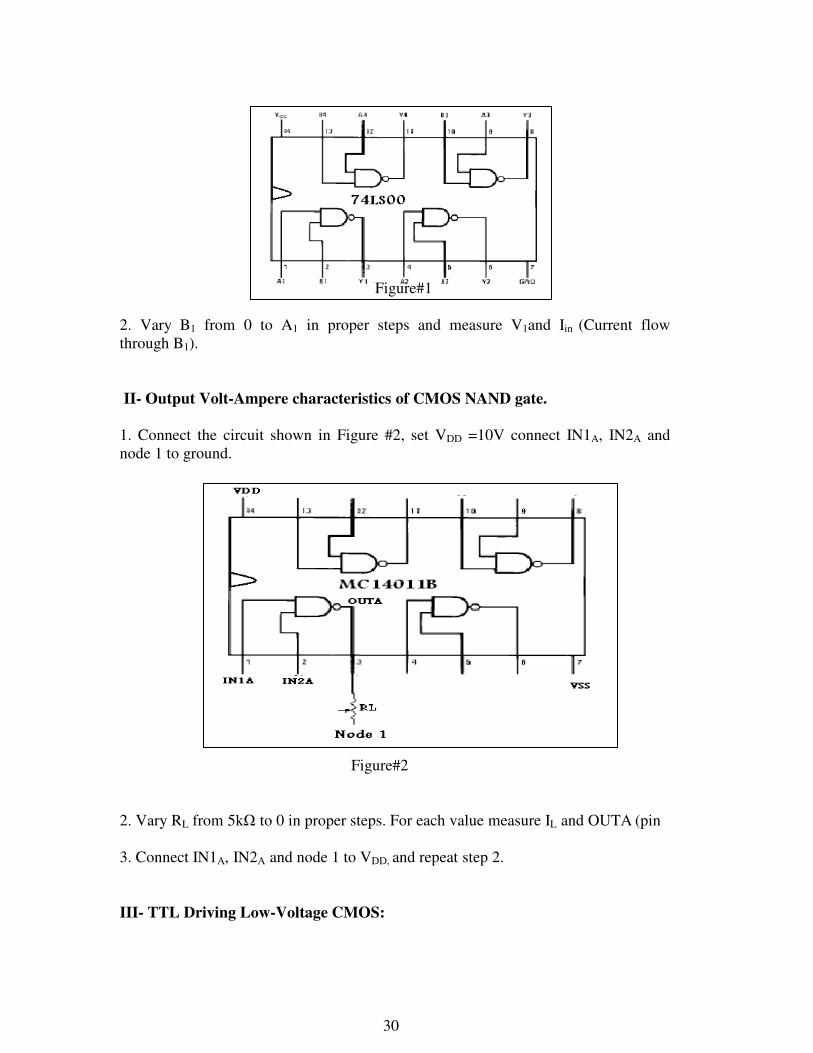
1. Connect the circuit shown in Figure#1, set VCC = A1 = 5.
30
Figure#1
2. Vary B1 from 0 to A1 in proper steps and measure V1and Iin (Current flow
through B1).
II- Output Volt-Ampere characteristics of CMOS NAND gate.
1. Connect the circuit shown in Figure #2, set VDD =10V connect IN1A, IN2A and
node 1 to ground.
Figure#2
2. Vary RL from 5kΩ to 0 in proper steps. For each value measure IL and OUTA (pin
3. Connect IN1A, IN2A and node 1 to VDD, and repeat step 2.
III- TTL Driving Low-Voltage CMOS:
31
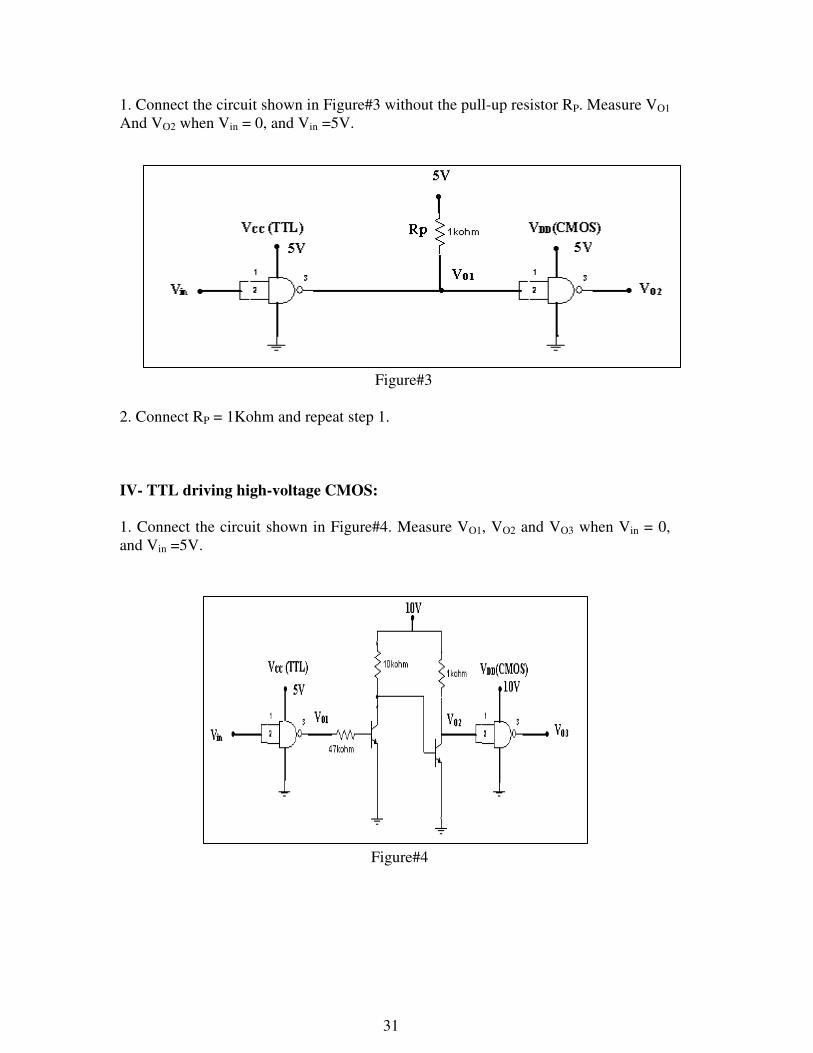
1. Connect the circuit shown in Figure#3 without the pull-up resistor RP. Measure VO1
And VO2 when Vin = 0, and Vin =5V.
Figure#3
2. Connect RP = 1Kohm and repeat step 1.
IV- TTL driving high-voltage CMOS:
1. Connect the circuit shown in Figure#4. Measure VO1, VO2 and VO3 when Vin = 0,
and Vin =5V.
Figure#4
32
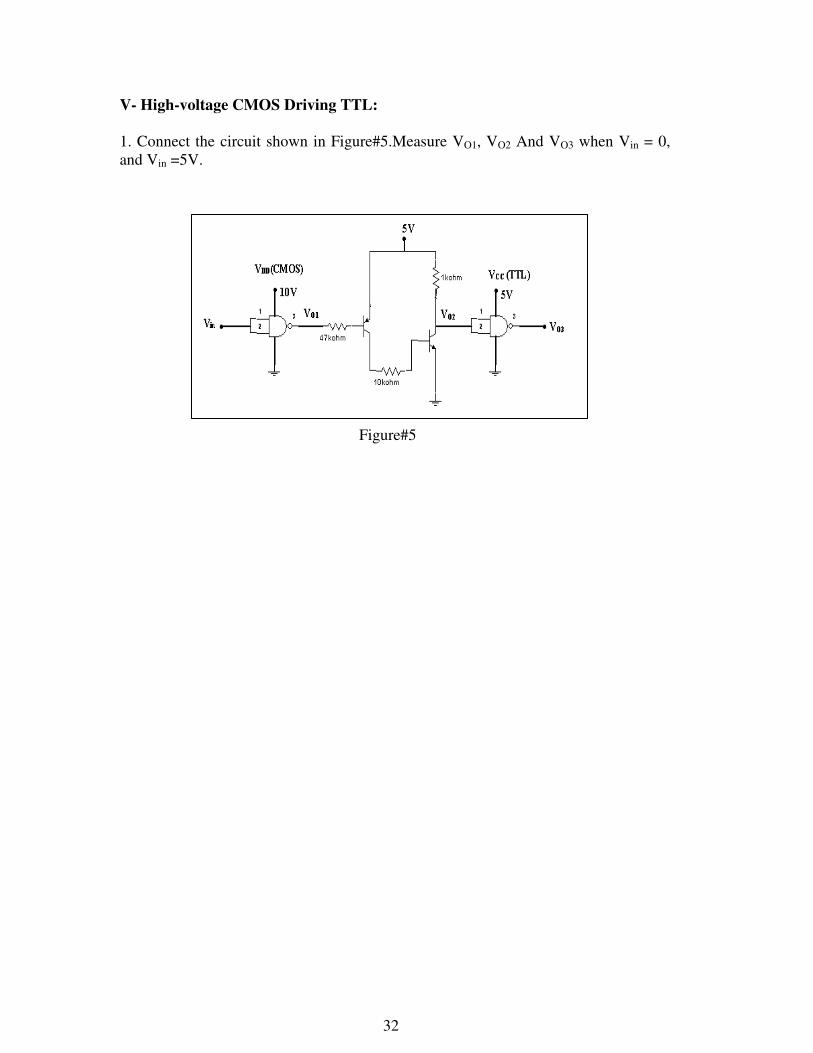
V- High-voltage CMOS Driving TTL:
1. Connect the circuit shown in Figure#5.Measure VO1, VO2 And VO3 when Vin = 0,
and Vin =5V.
Figure#5
33
xperiment#9E
Multivibrators Using 555 Timer
Introduction:
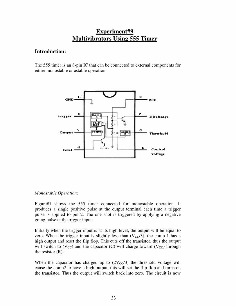
The 555 timer is an 8-pin IC that can be connected to external components for
either monostable or astable operation.
Monostable Operation:
Figure#1 shows the 555 timer connected for monostable operation. It
produces a single positive pulse at the output terminal each time a trigger
pulse is applied to pin 2. The one shot is triggered by applying a negative
going pulse at the trigger input.
Initially when the trigger input is at its high level, the output will be equal to
zero. When the trigger input is slightly less than (VCC/3), the comp 1 has a
high output and reset the flip flop. This cuts off the transistor, thus the output
will switch to (VCC) and the capacitor (C) will charge toward (VCC) through
the resistor (R).
When the capacitor has charged up to (2VCC/3) the threshold voltage will
cause the comp2 to have a high output, this will set the flip flop and turns on
the transistor. Thus the output will switch back into zero. The circuit is now
34
back to its initial condition and will remain there until another trigger pulse
occurs.
The larger the time constant (RC), the longer it takes the capacitor voltage to
reach (2VCC/3). In other words, the (RC) time constant controls the duration of
the output pulse (T),
3ln××= CRT
Astable Operation:
Figure #2 shows the 555 timer connected as astable operation. When the flip
flop is low the transistor is cutoff and the capacitor charges with time constant
equal to (R1+R2)C. the capacitor voltage rises until it goes slightly above
(2VCC/3). At this moment the comp2 will has a high output voltage, this
voltage drives comp2 to trigger the flip flop so that the output at pin 3 goes
low. In addition the transistor is driven on causing the output at pin 7 to
discharge the capacitor (C) through the resistor (R2), when the capacitor
voltage decreases below (VCC/3) the comp 1 will has a high output voltage.
This high voltage will reset the flip flop and causes the output at pin 3 to go
back high.
( ) 2ln21 RRCTch +=
2ln2 ××= RCTdch
dchch TTT +=
Tf
1=
Duty cycle (D) is used to specify how unsymmetrical the output is, and it is
given by:
%100×=T
TchD
Objectives:
1. To demonstrate the use of 555 timer as monostable and astable
35
multivibrators.
2. To design an astable 555 timer with specific frequency and duty
cycle.
Equipments and components: - DMM, OSC, FG, PS
- 555 Timer.
- Resistors: Decade resistance box, 1k Ω.
- Capacitors: 1µF, 0.1µF, 0.01µF, and 0.001µF
Procedure:
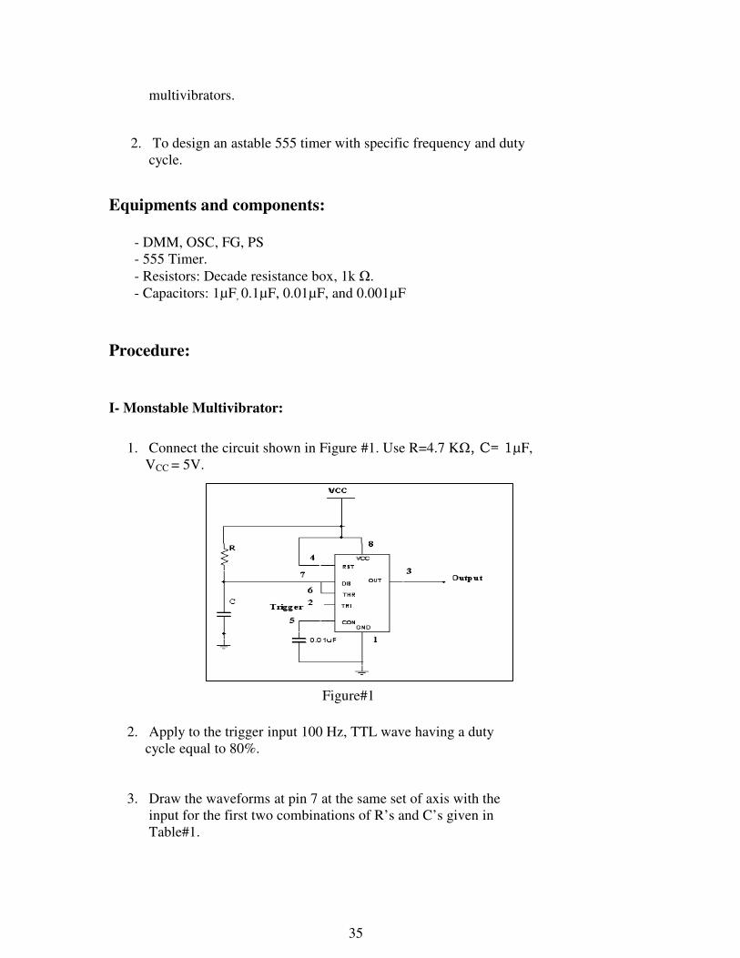
I- Monstable Multivibrator:
1. Connect the circuit shown in Figure #1. Use R=4.7 KΩ, C= 1µF,
VCC = 5V.
Figure#1
2. Apply to the trigger input 100 Hz, TTL wave having a duty
cycle equal to 80%.
3. Draw the waveforms at pin 7 at the same set of axis with the
input for the first two combinations of R’s and C’s given in
Table#1.
36
4. Measure the pulse width and the amplitude for the voltage at pin 3 and
pin 7.
5. Design a monostable multivibrator circuit which has a pulse width
equal to T= 4 ms.
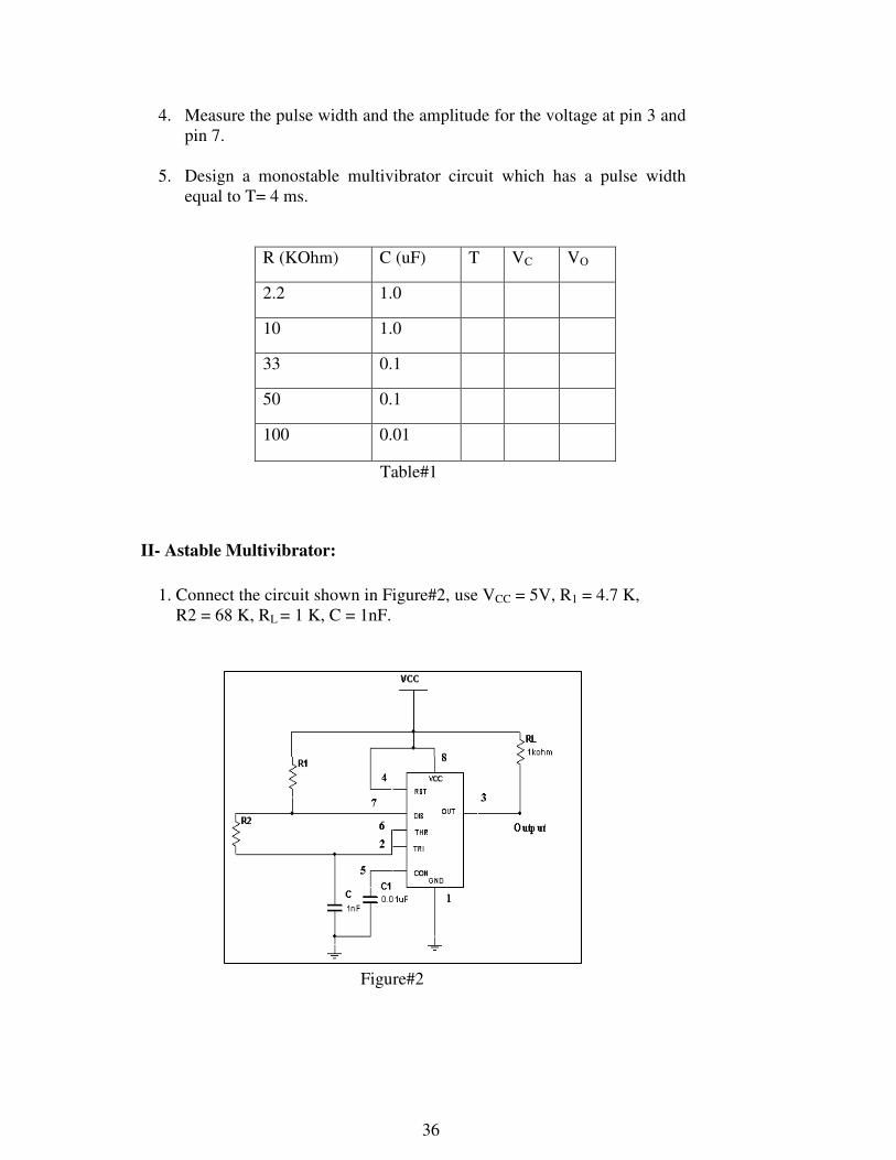
R (KOhm) C (uF) T VC VO
2.2 1.0
10 1.0
33 0.1
50 0.1
100 0.01
Table#1
II- Astable Multivibrator:
1. Connect the circuit shown in Figure#2, use VCC = 5V, R1 = 4.7 K,
R2 = 68 K, RL = 1 K, C = 1nF.
Figure#2

37
6. Draw the waveforms at pin 6 at the same set of axis with the output at
pin 3 for the first two combinations of R’s and C’s given in Table#2.
7. Measure Tch, Tdch, VC min, VC max for all R’s in Table#2.
8. Design an astable multivibrator circuit that has a duty cycle 65% and a
frequency of 80 KHz. Use a 1 nF capacitor.
R1
(Kohm)
R2
(Kohm)
Tch Tdch VC min VC max VO
4.7 68
6.8 18
12 33
10 100
Table#2
38
Experiment#10
Schmitt Trigger Characteristics
d Waveform GenerationAn
Introduction:
Schmitt trigger is a bistable multivibrator exhibits hysteresis in its transfer
characteristics. The bistable multivibrator as its name indicates has two stable
states and can remain in either stable state indefinitely and move to the other
state only when appropriately triggered. The Schmitt trigger can be
constructed using transistors or op-amp also it's available as digital integrated
circuits (IC's). The gates 7414 and 7413 are TTL Schmitt trigger, 40106 is a
CMOS one.
Op-amp Schmitt trigger circuit with inverting transfer characteristics:
The circuit shown in Figure#1 illustrates a Schmitt trigger with input voltage
applied to the inverting input terminal of the op=amp. To derive its transfer
characteristics (Vo versus Vin), assume that the op-amp output is saturated at
L+
and so,1
+×+
= LRR
RVref
21
1
Now as Vin is increased nothing happens until Vin is nearly equal to Vref. As
Vin begins to exceed Vref ,a net negative voltage develops between the input
terminals of the op-amp. This voltage is amplified by the open-loop gain of
the op-amp, and thus Vo goes negative. The voltage divider (R1, R2) in turns
causes Vref to go negative and thus increasing the net negative voltage input of
the op-amp. This process culminates in the op-amp saturating in the negative
direction that is with Vo= L- and correspondingly
−×+
= LRR
RVref
21
1
Now as Vin is decreased nothing happens until Vin is nearly equal to Vref. As
Vin begins to exceed Vref ,a net positive voltage develops between the input
terminals of the op-amp. This voltage is amplified by the open-loop gain of
the op-amp, and thus Vo goes positive and so saturating the op-amp in the
positive direction that is Vo = L+.
1 The saturation level of the op-amp is about 1.5V less than the bias supply voltage.
39
The electronic symbol for Schmitt trigger is shown below:
Generation of square wave using CMOS Schmitt trigger oscillator.
The Schmitt trigger can be used to generate a square wave by connecting it
with an RC circuit in a feed-back loop as shown in Figure#2. Observe that the
Schmitt trigger is a CMOS inverting type connected in oscillator circuit that is
it has no stable state and thus is appropriately named as an astable
mutivibrator.
The 40106 has VTH and VTL which vary with the supply voltage VDD. Vcap will
consists of alternating charging and discharging portion and Vo will be
rectangular pulse wave form whose period and pulse duration depends on R,
C, L+, L
-, VTH and VTL.
−
−=
+
+
TH
TL
chVL
VLT lnτ
−
−=
−
−
LV
LVT
TL
TH
dch lnτ
Where:
τ: is the time constant =RC.
VTL, VTH : The lower and upper threshold voltages
L+, L
-: The upper and Lower saturation levels.
Transistor Sweep Generator
A sweep voltage wave form is one whose voltage starts from a baseline and
increases at a uniform linear rate up to a peak amplitude, then rapidly returns
to it's baseline voltage, a sweep wave form is also referred to as saw tooth or
time-base waveform.
Figure#3 shows a sweep wave form generator in which a pnp transistor is
used to charge the capacitor and a npn transistor switch is used to discharge it.
40
The pnp transistor is connected in common base configuration and it is used to
operate in the active region. Assume the capacitor is initially discharged so the
collector (C1) is at ground potential. Since the base is biased at VBB above the
ground, the C-B junction of Q1 is reversed based with VCB=-VBB.
Objectives: 1. To demonstrate the characteristics of op-amp Schmitt trigger.
2. To generate square wave using Schmitt trigger.
Equipments and components:
- DMM, OSC, FG, PS
- CMOS Schmitt trigger 40106
- Op-Amp 741
- Transistors BJT NPN, PNP.
- Resistors: 10 k Ω, 6.8 k Ω, 4.7 k Ω , 2.2 k Ω, and 1k Ω .
-Capacitors: 0.1 nF, and 4.7 nF
Experimental Procedure:
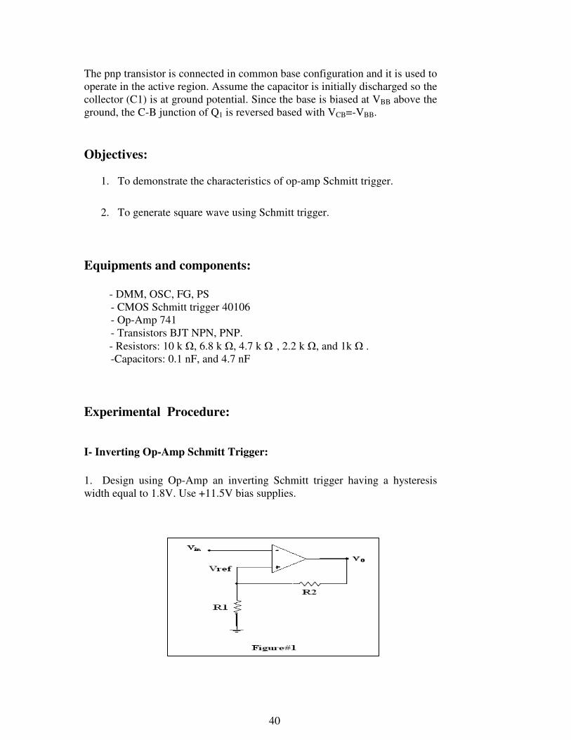
I- Inverting Op-Amp Schmitt Trigger:
1. Design using Op-Amp an inverting Schmitt trigger having a hysteresis
width equal to 1.8V. Use +11.5V bias supplies.

41
2. Apply a sine wave with frequency= 1 KHz at 5 VP-P at the input terminal.
Sketch the transfer characteristics.
3. Measure L+, L-, VTH, VTL for the transfer characteristics.
4. Change the value of bias supplies as given below and repeat step 3.
II. Generation of Square wave using CMOS Schmitt trigger (40106).
1. Connect the circuit shown in Figure#2, use VDD= 10V.
2. Sketch the waveform Vcap and Vo .
3. Measure Tch and Tdch for Vcap . Calculate the Duty cycle.
4. Measure L+, L-, VTH and VTL.
V+ 15 11.5 8 11.5
V- -11.5 -15 -11.5 -8

42
III. Generation of sweep waveform.
1. Connect the circuit shown in Figure#3. Apply at the input a TTL wave of frequency
20 KHz and 0.2 Duty cycle.
2. Sketch VO and VIN at the same set of axis
3. Change the frequency to 200 Hz and note the effect on the output voltage