Embed Size (px)
Citation preview
DEPARTMENT OF ELECTRICAL & COMPUTER ENGINEERING
OLD DOMINION UNIVERSITY
PH.D. DIAGNOSTIC EXAM
Fall 2014
ODU HONOR PLEDGE
I pledge to support the Honor system of Old Dominion University. I will refrain from any form of academic
dishonesty or deception, such as cheating or plagiarism. I am aware that as a member of the academic
community, it is my responsibility to turn in all suspected violators of the Honor Code. I will report to a
hearing if summoned.
Student Signature: ___________________________________________________
Student Name (BLOCK CAPITALS): ___________________________________
UIN Number: _________________________________________________
Please turn in this examination document with the pledge above signed and with one answer book for each
solved problem.
1. This examination contains 26 problems from the following six areas:
A. MATH (At most 3 problems can be A1 A2 A3 A4
answered from the Math area)
B. CIRCUITS & ELECTRONICS B1 B2 B3
C. SYSTEMS, SIGNAL AND IMAGE PROCESSING C1 C2 C3 C4 C5 C6
D. PHYSICAL ELECTRONICS I D1 D2 D3 D4
E. PHYSICAL ELECTRONICS II E1 E2 E3
F. COMPUTER SYSTEMS F1 F2 F3 F4 F5 F6
2. You must answer Eight problems, but no more than three from the MATH group.
3. Answer in the blue books provided. Use a separate book for each problem. Put the title and
problem number on the front of each book (eg., MATH A-1) 4. Return all the 26 problems.
5. You will be graded on your answers to Eight problems only.
6. The examination is “closed-book;” only blue books, exam problems and a scientific calculator are
allowed. No formula sheet is allowed. Some problems include reference formulas. No material shall
be shared without prior permission of the proctor(s).
7. You have four hours to complete this examination.

PROBLEM A1 – MATH
Complex Variables and Differential Equations
Integrate a complex function f(z) in the counterclockwise sense around a circle of radius 1 with
center at the point z=i. f(z) is shown in the following:
f(z)=𝑧2+1
𝑧2−1

PROBLEM A2 – MATH
Vector Calculus
Consider the vector field
𝐴(𝑥, 𝑦) = (−𝑥
𝑦)
(a) Make a sketch of 𝐴(𝑥, 𝑦). You do not need to be numerically accurate, but you need to capture the qualitative
features of 𝐴.
(b) Compute curl(𝐴) and interpret your result.
(c) Is there a function 𝑓(𝑥, 𝑦) so that 𝐴(𝑥, 𝑦) = grad(𝑓)? If yes, provide such an 𝑓. If no, explain why not.
Good luck!
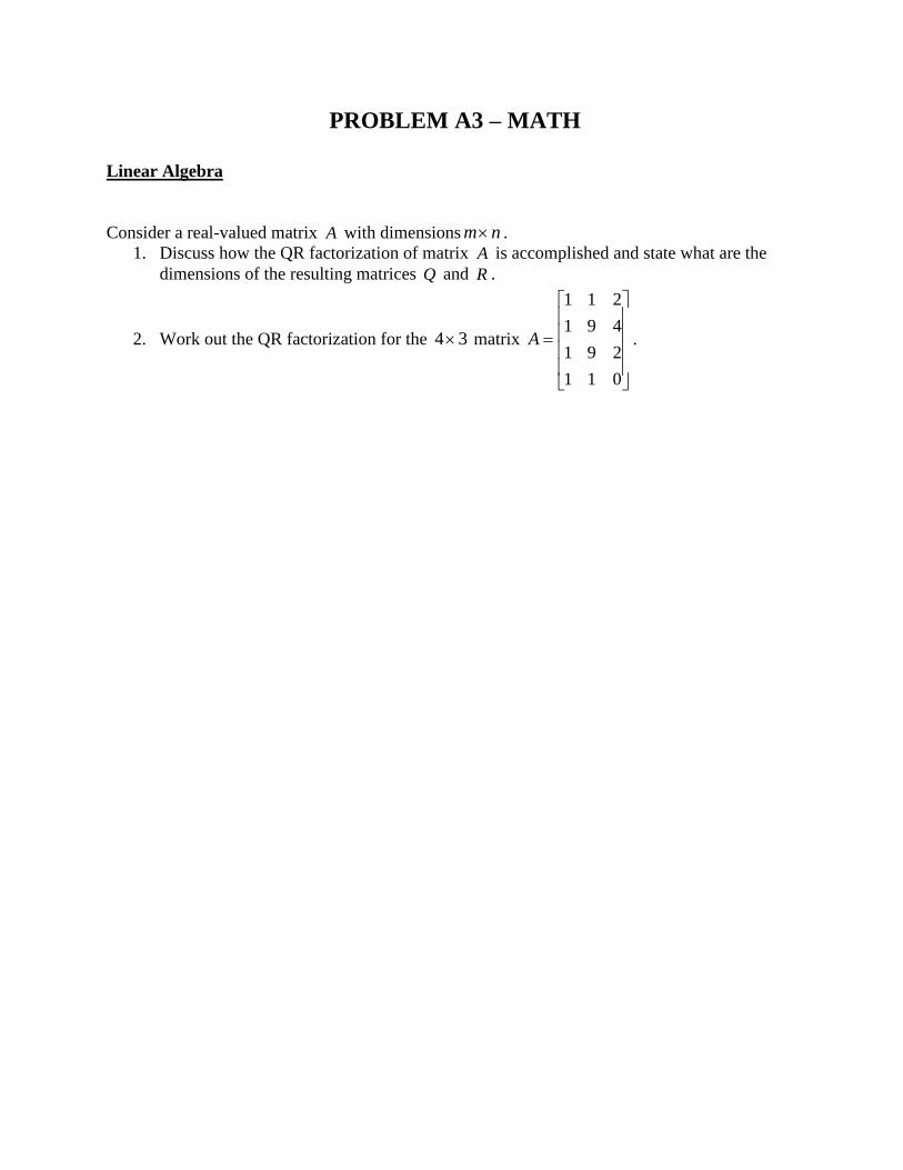
PROBLEM A3 – MATH
Linear Algebra
Consider a real-valued matrix A with dimensions nm .
1. Discuss how the QR factorization of matrix A is accomplished and state what are the
dimensions of the resulting matrices Q and R .
2. Work out the QR factorization for the 34 matrix
011
291
491
211
A .

PROBLEM A4 – MATH
Probability
(1). Given P(E U Fc)c = 0.37, P(Fc) = 0.61, and P(E) = 0.27. Find P(Fc | Ec).
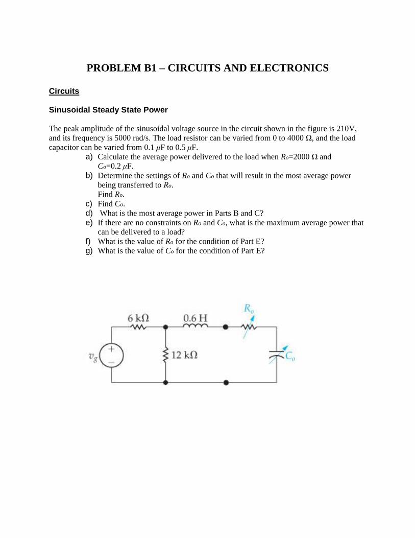
PROBLEM B1 – CIRCUITS AND ELECTRONICS
Circuits Sinusoidal Steady State Power The peak amplitude of the sinusoidal voltage source in the circuit shown in the figure is 210V,
and its frequency is 5000 rad/s. The load resistor can be varied from 0 to 4000 Ω, and the load
capacitor can be varied from 0.1 μF to 0.5 μF. a) Calculate the average power delivered to the load when Ro=2000 Ω and
Co=0.2 μF. b) Determine the settings of Ro and Co that will result in the most average power
being transferred to Ro.
Find Ro. c) Find Co. d) What is the most average power in Parts B and C? e) If there are no constraints on Ro and Co, what is the maximum average power that
can be delivered to a load? f) What is the value of Ro for the condition of Part E? g) What is the value of Co for the condition of Part E?
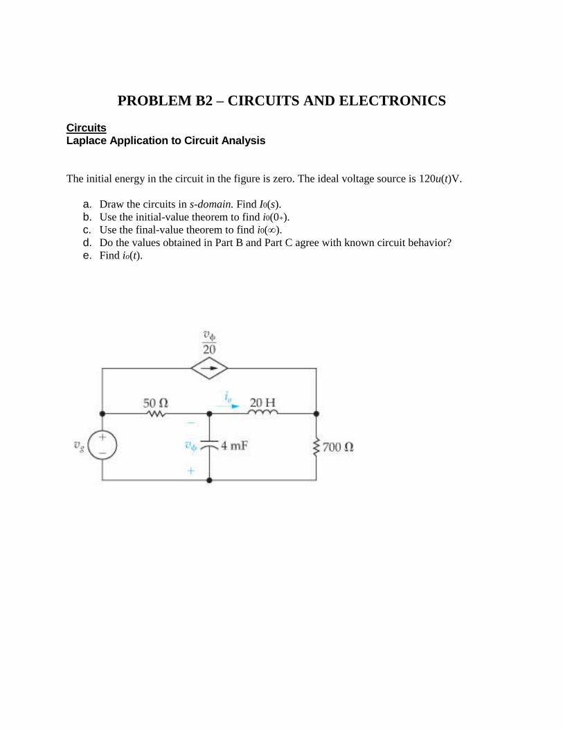
PROBLEM B2 – CIRCUITS AND ELECTRONICS Circuits Laplace Application to Circuit Analysis The initial energy in the circuit in the figure is zero. The ideal voltage source is 120u(t)V.
a. Draw the circuits in s-domain. Find I0(s). b. Use the initial-value theorem to find i0(0+). c. Use the final-value theorem to find i0(∞). d. Do the values obtained in Part B and Part C agree with known circuit behavior? e. Find io(t).
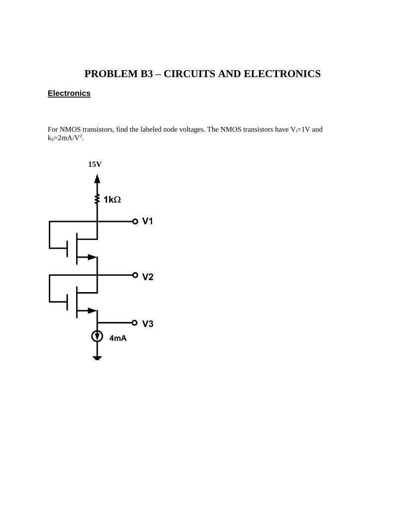
PROBLEM B3 – CIRCUITS AND ELECTRONICS
Electronics
For NMOS transistors, find the labeled node voltages. The NMOS transistors have Vt=1V and
kn=2mA/V2.
15V
PROBLEM C1 – SYSTEMS, SIGNALS AND IMAGE
PROCESSING
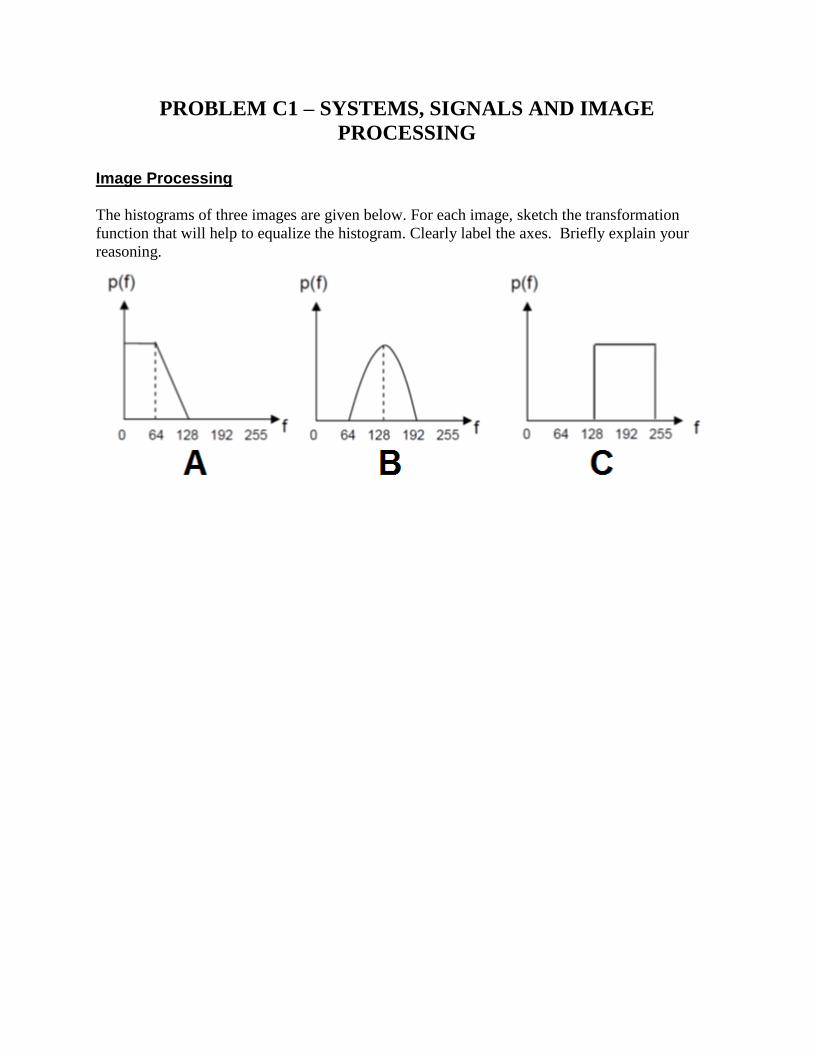
Image Processing The histograms of three images are given below. For each image, sketch the transformation
function that will help to equalize the histogram. Clearly label the axes. Briefly explain your
reasoning.

PROBLEM C2 – SYSTEMS, SIGNALS AND IMAGE
PROCESSING Digital Signal Processing
A discrete-time system is given by
]1[
][]1[
nx
nxny
a) (4 points) Is the system BIBO stable? Justify your answer.
b) (3 points) Is the system memoryless? Justify your answer.
c) (3 points) Is the system causal? Justify your answer.

PROBLEM C3 – SYSTEMS, SIGNALS AND IMAGE
PROCESSING
Digital Signal Processing
4). If a continuous time signal xc(t) is band limited to 5kHz and you want to design a low-pass
filter with a cutoff frequency of 4kHz for the signal but in the discrete-time domain. The signal is
sampled at a sampling rate of 20000 samples per second to obtain a discrete-time signal x[n].
a). (5 points) What is the highest frequency component in x[n]?
b). (5 points) What is the cutoff frequency of the discrete-time low-pass filter?
PROBLEM C4 – SYSTEMS, SIGNALS AND IMAGE
PROCESSING
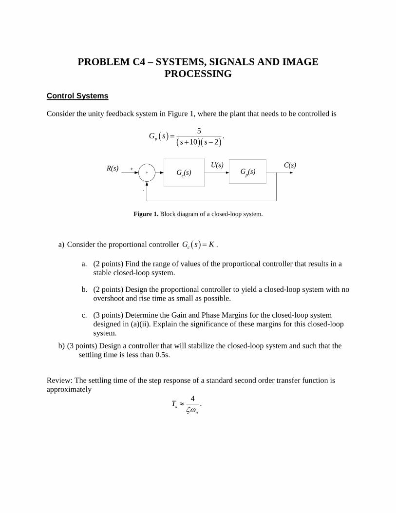
Control Systems
Consider the unity feedback system in Figure 1, where the plant that needs to be controlled is
5.
10 2pG s
s s
R(s) C(s)G
p(s)G
c(s)+
+
-
U(s)
Figure 1. Block diagram of a closed-loop system.
a) Consider the proportional controller cG s K .
a. (2 points) Find the range of values of the proportional controller that results in a
stable closed-loop system.
b. (2 points) Design the proportional controller to yield a closed-loop system with no
overshoot and rise time as small as possible.
c. (3 points) Determine the Gain and Phase Margins for the closed-loop system
designed in (a)(ii). Explain the significance of these margins for this closed-loop
system.
b) (3 points) Design a controller that will stabilize the closed-loop system and such that the
settling time is less than 0.5s.
Review: The settling time of the step response of a standard second order transfer function is
approximately
4
.n
sT
PROBLEM C5 – SYSTEMS, SIGNALS AND IMAGE
PROCESSING
Communication systems
1. Sketch the block diagram of the noisy receiver model and explain how the output signal-
to-noise-ratio is defined for both liner and non-linear demodulators.
2. Sketch the block diagram of the baseband transmission model and write the expression of
the baseband signal-to-noise-ratio.
3. Sketch the block diagram of the noisy communication channel with attenuation and write
the expression of the received signal for this model in terms of the transmitted signal, the
attenuation coefficient, and the noise process that corrupts the transmitted signal at the
receiver. Define also the power loss factor for this model and write its expression as a
function of the attenuation coefficient.

PROBLEM C6 – SYSTEMS, SIGNALS AND IMAGE
PROCESSING
Communication Networks
1. (5 points) A frame contains 2000 bits. To detect the error for transmitting this frame, what is
the minimum number of redundancy bits (or error detect bits) required?
2. (5 points) For a channel with 10 MHz bandwidth, if the signal to noise ratio is 30 dB, what is
the maximum data rate that can be achieved on this channel?
PROBLEM D1 – PHYSICAL ELECTRONICS I
Electromagnetics
(1). A perpendicularly polarized wave propagates from region 1 (εr1 = 8.5, μr1 = 1, σ1 = 0) to
region 2 (free space), with an angle of incidence of 15◦. Given E0i = 1 μV/m, find: E0
r , E0t,
H0i, H0
r , and H0t.

PROBLEM D2 – PHYSICAL ELECTRONICS I
Electromagnetics
Assume a hydrogen atom that has an electron in the innermost orbit. Find the potential energy,
the kinetic energy and the total energy for the electron of a hydrogen atom in terms of unit
charge q, orbit radius r, and permittivity .
PROBLEM D3 – PHYSICAL ELECTRONICS I Lasers
A population of identical two-level atoms is in thermal equilibrium. The population distribution
between the two states ∑g (ground state) and ∑e (excited state) is following the Boltzmann
distribution. With Ng and Ne referring to the population densities of states ∑g and ∑e respectively
solve the following: 1. Calculate Ne/Ng for an optical transition at a wavelength of 600 nm with the atom population at
27 oC (h/2π = 1.1 x 10⁻³⁴ J.s and kB = 1.4 x 10⁻²³ J/K). (10 points)
2. At what temperature will Ne be equal to 0.01 Ng? (5 points)
3. Can this system at any temperature provide gain to optical radiation? Why or why not? (5
points)
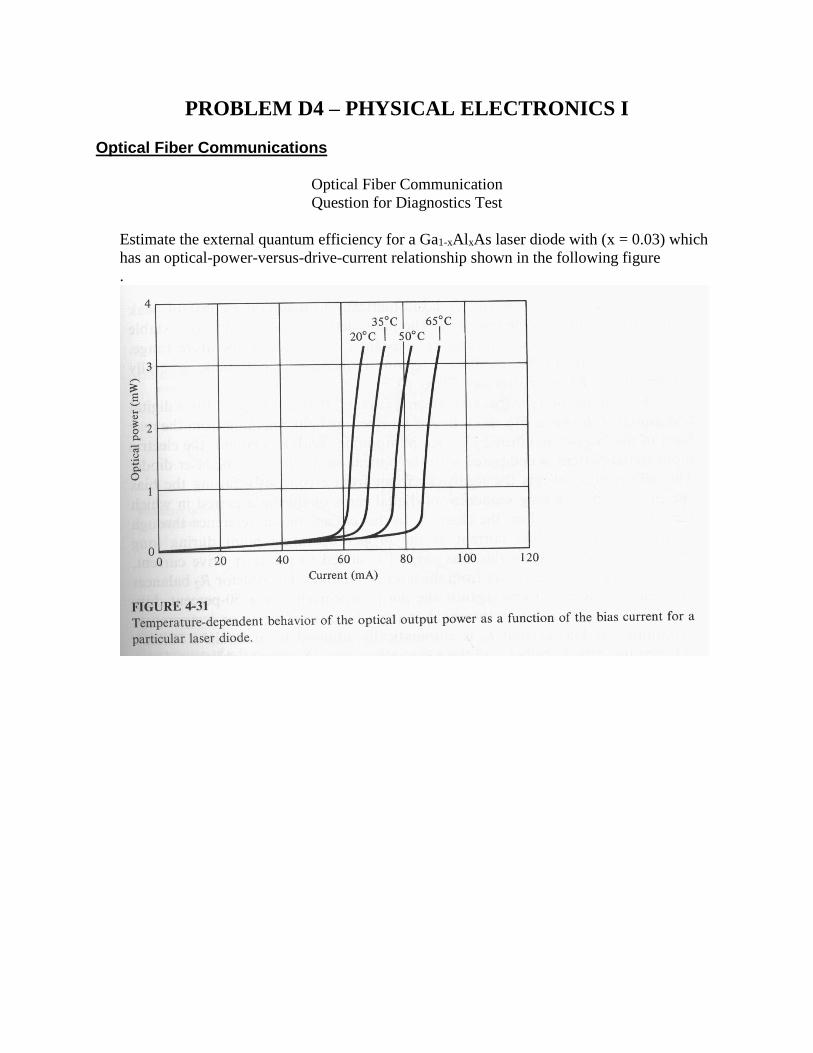
PROBLEM D4 – PHYSICAL ELECTRONICS I
Optical Fiber Communications
Optical Fiber Communication
Question for Diagnostics Test
Estimate the external quantum efficiency for a Ga1-xAlxAs laser diode with (x = 0.03) which
has an optical-power-versus-drive-current relationship shown in the following figure
.
PROBLEM E1 - PHYSICAL ELECTRONICS II
Solid State Electronics
An abrupt Si P-N Junction with a cross-section of A = 10-4 cm2 has the following
properties:
P side N side
Na = 1017 cm-3 Nd = 1015 cm-3
τ n = 0.1 µs τp = 10 µs
µp = 200 cm2/ V-s µn = 1300 cm2/ V-s
µn = 700 cm2/ V-s µp = 450 cm2/ V-s
The junction is forward biased by 0.5 V.
a) What is the total forward current for an ideal p-n junction at + 0.5V bias? (Need to calculate Dp, Dn, Lp, Ln, pn, np)
b) What is the total current at a reverse bias of – 0.5V?
c) Calculate the junction potential also called built-in potential 𝑉𝑏𝑖
d) What is the total depletion capacitance (𝐶𝑗) at -4 V reverse bias?
e) Calculate the depletion widths on the p-side of the junction Xp and on the n-side Xn for the following reverse biases -4 V and -10 V
Equations:
Ideal diode: I = qA (𝐷𝑝
𝐿𝑝𝑃𝑛 +
𝐷𝑛
𝐿𝑛𝑛𝑝)(𝑒𝑞𝑉 𝑘𝑇⁄ − 1) = 𝐼0(𝑒𝑞𝑉 𝑘𝑇⁄ − 1)
𝐷𝑝 =𝑘𝑇
𝑞𝜇𝑝 𝐿𝑝 = √𝐷𝑝𝜏𝑝
𝐷𝑛 =𝑘𝑇
𝑞𝜇𝑛 𝐿𝑛 = √𝐷𝑛𝜏𝑛

𝑋𝑝 = √2𝜀𝑠𝑖
𝑞(𝑉𝑏𝑖 − 𝑉)
𝑁𝑑
𝑁𝑎(𝑁𝑎 + 𝑁𝑑)
𝜀𝑠𝑖 = 𝜀 ∗ 𝐾𝑠𝑖
𝑋𝑛 = √2𝜀𝑠𝑖
𝑞(𝑉𝑏𝑖 − 𝑉)
𝑁𝑎
𝑁𝑑(𝑁𝑎 + 𝑁𝑑)
Total depletion width
W=𝑋𝑝 + 𝑋𝑛=√2𝜀𝑠𝑖
𝑞(𝑉𝑏𝑖 − 𝑉)
(𝑁𝑎+𝑁𝑑)
𝑁𝑎∙𝑁𝑑
Depletion Capacitance:
𝐶𝑗 = √𝜀𝑆𝑖𝐴 [𝑞
2(𝑉𝑏𝑖 − 𝑉)
𝑁𝑑𝑁𝑎
𝑁𝑑 + 𝑁𝑎]
12⁄
Physical Constants :
Intrinsic carrier concentration in Si : ni = 1.45 x 1010 cm -3
Permittivity in Vacuum ε = 8.8854 x 10⁻¹⁴ F/ cm ;
Dielectric constant of 𝑆𝑖 𝐾𝑠𝑖 = 11.7
Elementary Charge : q = 1.602 x 10⁻¹⁹ C
Boltzman Constant: k = 1.38066 x 10 -23 J/ K = 8.62*10−5𝑒𝑉/𝐾
Thermal voltage at 300K: kT/q = 0.0259 V

PROBLEM E2 – PHYSICAL ELECTRONICS II
Physical Electronics
1. MCQ question
Circle all of the answers that are correct. There is at least one answer correct, but there could be
several.
The total current in a p-n junction at thermal equilibrium is
a. due partly to the electron drift
b. due partly to the holes diffusion
c. positive
d. negative
2. For a silicon one sided abrupt junction with NA=1018 cm-3 and ND=1015 cm-3, calculate the
depletion layer width, the maximum field and the junction capacitance at zero bias and
reverse bias of 3V (T = 300K)
Equations: s = 105 10-14 F/cm
Silicon (300 K): NC= 2.86 1019 cm-3 ; NV = 2.66 1019 cm-3 ; ni = 9.65 109 cm-3
mp =1 m0; mn = 0.19 m0; m0 = 0.91 10-30 kg; k = 1.38 10-23 J/K ; q = 1.6 10-19 C

PROBLEM E3 – PHYSICAL ELECTRONICS II
Plasma Science and Discharges
Problem 1. (a) 3 points, (b)-(d) 1.5 points each
(a) Sketch a diagram of the different regions of a DC glow discharge. Show the following: The cathode dark
space, the negative glow, the Faraday dark space, and the positive column. (b) Which region of the discharge is best described as plasma? Explain why. (c) In which region most of the potential is dropped. (d) In a glow discharge, the current is carried mainly by electrons except in one of the above-mentioned regions,
where it is mainly due to ions. Which region is that? (e) If a cold cathode is replaced by a hot filament emitting electrons, how would this change the operating E/n
(reduced electric field, where E is electric filed and n is the gas density) for a fixed discharge geometry? Explain why.
PROBLEM F1 - Computer Systems Microprocessors
An ODU PhD student designed an 8-bit processor with the following instruction set:
Instruction Operands Description MOVE regD, immediate( regS ) regD = Mem[ immediate + regS ]
MOVEI regD, #immediate regD = immediate
MOVEM $address, regS Mem[address] = regS
MOVEX Immediate(regD), regS Mem[ immediate + regD ] = regS
ADD regD, regS regD = regD + regS
SUB regD, regS regD = regD – regS
AND regD, regS regD = regD and regS (bitwise and)
OR regD, regS regD = regD or regS (bitwise or)
NOT regD regD = not regD (bitwise not)
EOR regD, regS regD = regD xor regS (bitwise exclusive or)
LSL regD, regS regD = regD << regS (Logic shift left)
LSR regD, regS regD = regD >> regD (Logic shift right)
CMP regD, regs regD – regS
CMPI regD, #immediate regD – immediate
BEQ $address Branch to address if equal
BNE $address Branch to address if not equal
BLT $address Branch to address if less than
BGT $address Branch to address if greater than
JMP $address Jump unconditionally to address
JSR $address Jump to subroutine at the given address
RTS $address Return from subroutine
This processor has 8 general purpose registers (D0, D1, … , D7) (8-bit each). It also has an 8-bit data bus and a 16-bit
address bus. The student has the following components connected to the microprocessor.
A DIP (Dual In-line Package) switch (8-switches package) and its interfacing circuit are memory mapped to the byte at address $A000. The switch is used to accept 8 bit binary input from the user and store it at that memory address.
An 8 LED (Light-Emitting Diode) array with its interfacing circuit are mapped to the byte at memory location $A010. Whenever a byte is written to that memory address, it is displayed on the LED array.
A push button and its interfacing circuit are memory mapped to bit 3 of the byte at memory location $A020. Pressing the push button corresponds to setting bit 3 of address $A020 to 1, and when the button is released the bit is set to 0. The push button output is sampled every 1ms.
Given the above information, answer the following questions:
1. What are the supported addressing modes for this processor?
2. What is the maximum memory size that can be interfaced with this processor?
3. Write an assembly routine that reads 10 numbers, each is an unsigned byte, from the DIP switch and store them as an array in memory starting from address $8000. An number is read from the DIP switch when bit 3 of address $A020 changes its value from 0 to 1, i.e., whenever the push button is pushed from its release state. Once all the 10 numbers are entered, the sum is calculated, then the values $00, $FF, and $00 are passed to the LED array respectively. After that the calculated sum is passed to the LED array. The LED array will continue showing the sum until the routine is restarted. The routine is restarted when the value of bit 3 at address $A020 changes 3 times from 0 to 1, i.e., the push button has been pushed and released three times. (You can assume that your code is a position-independent. You are allowed to use labels )
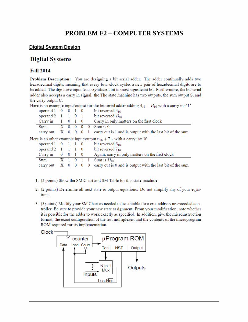
PROBLEM F2 – COMPUTER SYSTEMS
Digital System Design

PROBLEM F3 – COMPUTER SYSTEMS
Computer Architecture
Draw a pipeline diagram based on basic 5-stage pipeline to trace the execution of the following
instructions. Show any forwarding paths or stalls.
ADD $t0, $t1, $t2
SUBI $to, $to, 8
LW St3, 0($to)
ADD St4, $t3, $t3

PROBLEM F4 – COMPUTER SYSTEMS
Algorithms

PROBLEM F5 – COMPUTER SYSTEMS
Data Structures
ab+c-de*+
In here, * is the multiplication sign

PROBLEM F6 – COMPUTER SYSTEMS
Logic/Digital Circuits
1. (10 points) Given the following truth table,
A B C Y
0 0 0 1
0 0 1 1
0 1 0 0
0 1 1 1
1 0 0 1
1 0 1 1
1 1 0 0
1 1 1 0 (a) (4 pts) write the Boolean equation in sum-of-products form.
(b) (3 pts) Simplify the Boolean equation using Karnaugh map.
(c) (3 pts) Use either Verilog or VHDL to implement the simplified function.