Embed Size (px)
Citation preview
DESY PRC R&D 03/01 Update 1(05)Project: DEPFET for ILCType of Document: Status ReportDate: 2.5.2005
DEPFET Pixel Vertex Detector for the ILC1
R. Kohrs, M. Karagounis, H. Kruger, L. Reuen, C. Sandow,M. Trimpl, N. Wermes2
(Bonn University)
P. Fischer3, F. Giesen, I. Peric(Mannheim University)
L. Andricek, K. Heinzinger, P. Lechner, G. Lutz, H. G. Moser4,R. H. Richter, M. Schnecke, L. Struder, J. Treis
(MPI Munich, HLL)
1Work supported by the German Ministerium fur Bildung, Wissenschaft, Forschungund Technologie (BMBF) under contracts no. 05HS4VM1/5 and no. 05HS4PDA/6
Abstract
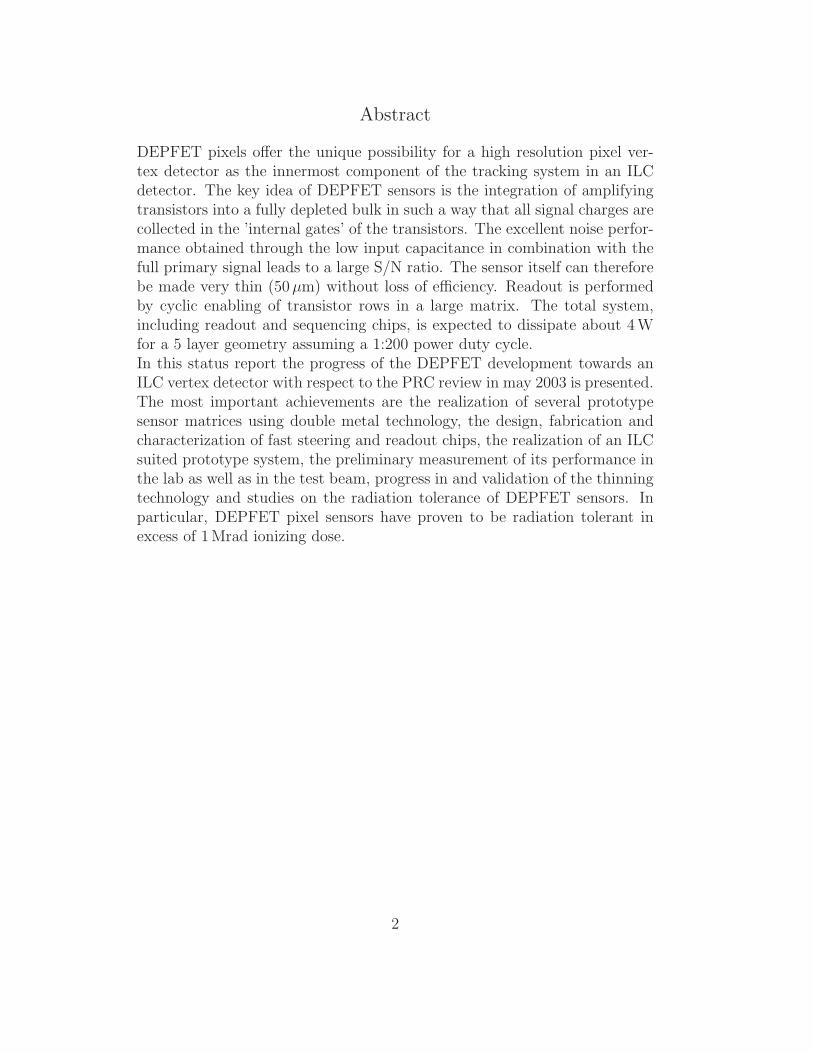
DEPFET pixels offer the unique possibility for a high resolution pixel ver-tex detector as the innermost component of the tracking system in an ILCdetector. The key idea of DEPFET sensors is the integration of amplifyingtransistors into a fully depleted bulk in such a way that all signal charges arecollected in the ’internal gates’ of the transistors. The excellent noise perfor-mance obtained through the low input capacitance in combination with thefull primary signal leads to a large S/N ratio. The sensor itself can thereforebe made very thin (50µm) without loss of efficiency. Readout is performedby cyclic enabling of transistor rows in a large matrix. The total system,including readout and sequencing chips, is expected to dissipate about 4 Wfor a 5 layer geometry assuming a 1:200 power duty cycle.In this status report the progress of the DEPFET development towards anILC vertex detector with respect to the PRC review in may 2003 is presented.The most important achievements are the realization of several prototypesensor matrices using double metal technology, the design, fabrication andcharacterization of fast steering and readout chips, the realization of an ILCsuited prototype system, the preliminary measurement of its performance inthe lab as well as in the test beam, progress in and validation of the thinningtechnology and studies on the radiation tolerance of DEPFET sensors. Inparticular, DEPFET pixel sensors have proven to be radiation tolerant inexcess of 1 Mrad ionizing dose.
2
1 Introduction
This status report summarizes the progress achieved towards a DEPFETpixel tracker suited for application at the ILC. The initial R&D, describedin the PRC report from may 2003, was oriented towards TESLA. The antic-ipated environment in ILC is very similar and the assumed boundary con-ditions remain valid. The general requirements for a vertex detector in thehigh multiplicity environment of the ILC and how they are addressed by aDEPFET system are summarized as follows:
⊲ Aim at a spatial point resolution per layer of . 2 − 4 µm. This isaddressed by pixels of 25× 25 µm2 size guaranteing a binary resolutionof 25 µm/
√12 ≈ 7 µm. Analog interpolation assuming an anticipated
signal to noise ratio of & 40 will significantly improve this value. With a64×64 matrix of the previous (non-ILC) DEPFET production with cellsizes of 50×50 µm2 a spatial resolution of 4.3±0.8 µm, obtained with a109Cd source (γ, 22 keV) and a S/N of 50, has been measured [7]. Theresolution for the ILC structures with pixel linear dimensions smallerby a factor 2 and a similar S/N value is expected to be much better.
⊲ Place the innermost layer at a radius of ≈ 15 mm. The active area inthis innermost layer must therefore have a length (along the beam) of≈ 10 cm. This requires 4096 pixels of 25µm height.
⊲ Sustain in the innermost layer an accumulated radiation dose after 5years of operation of 100 − 200 krad. Irradiation tests of DEPFETdevices suggest that the sensors are radiation tolerant well above thislimit.
⊲ Aim for a minimum radiation length to restrict multiple scattering.A thinning technology compatible with DEPFET production has beendeveloped. It will be used to thin the sensor in the active part to 50 µm.New measurements indicate that the leakage currents of sensor diodesare not degraded by the thinning procedure.
⊲ Operate at a bunch train repetition rates of 5 Hz with each train de-livering 2820 bunches during ≈ 1 ms. The low duty cycle of 1:200is exploited to reduce the average power dissipation of the system to≈ 4 W.
⊲ Tolerate a hit multiplicity of ≈ 0.03 hits per mm2 and bunch at√s = 500 GeV. Pixels of 25 × 25 µm2 size will therefore have a 7 %
hit occupancy in one train if 30 % of double hits are assumed. Thisoccupancy is probably unacceptable for cluster reconstruction and pat-tern recognition so that a sensor operated this close to the beam must
1
be read out several times during one bunch train. A line readout rate of40 MHz would decrease the occupancy by a convenient factor of 20 tobelow half a percent (for a sensor with 4096 pixels read out at the bot-tom and at the top). Smaller reduction rates at slower readout speedmay be tolerable.
⊲ Operate in a magnetic field of 4 T. The effect of the Lorentz angle isexpected to be small due to the thin sensor.
The main goals since the last PRC review in may 2003 were:
⊲ Characterization and test of all components of a DEPFET prototypemodule, e.g.
– the DEPFET sensor matrix
– the readout chip (CURO)
– the sequencer chip (SWITCHER)
⊲ Development of a prototype module including all above componentswith close to ILC specs
⊲ Further improvement of the thinning technology
⊲ Characterization of the radiation tolerance of all components, mostnotably of the DEPFET sensor itself
⊲ Operation and characterization of the prototype system in a test beam
Almost all of these goals have been achieved. They will be detailed in thefollowing sections. The report is organized as follows: Section 2 treats theDEPFET sensor. After a short introduction of the working principle, the pro-duction technology and some of the implemented structures are described.Results on thinned devices and after irradiation are presented. Some exam-ples of detailed studies on clear properties of single pixels are given. Section 3describes the readout system with the individual components, in particularthe steering and readout chips. Measurement results from the lab and froma test beam held at DESY are presented.
2 The DEPFET Sensor
2.1 DEPFET Principle and Operation
The DEPleted Field Effect Transistor structure, abbreviated DEPFET, pro-vides detection and amplification properties jointly. The concept was pro-posed in 1987 [1] and developed to a level of maturity in the nineties [2–7].
2
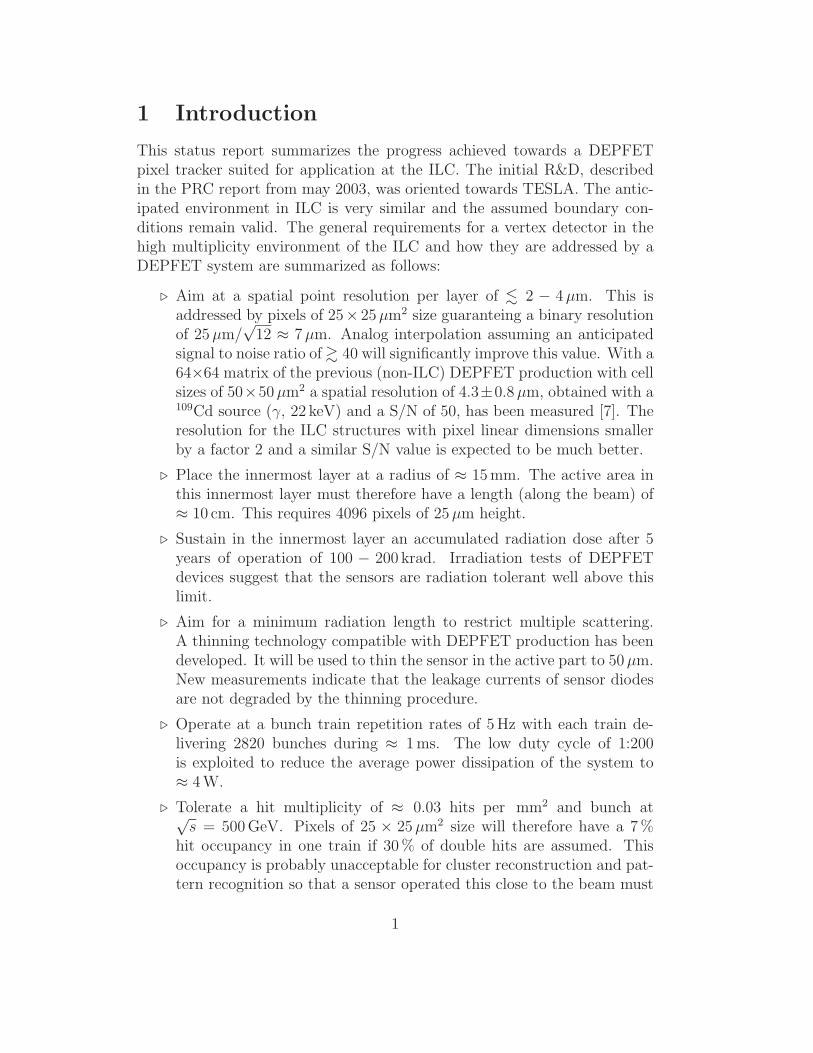
Figure 1: The DEPFET detector and amplification structure (c) is based ona sidewards depleted substrate material (a) into which a planar field effecttransistor (b) is embedded (a MOS device is shown here). The electric po-tential is schematically drawn on the right side with the p+-implants set toground
The DEPFET principle of operation is shown in Fig. 1. A MOS or junc-tion field effect transistor is integrated onto a detector substrate. By meansof sidewards depletion [8] and additional n-implants below the transistor apotential minimum for electrons is created underneath (≈ 1 µm) the transis-tor channel. This can be considered as an internal gate of the transistor. Aparticle entering the detector creates electron-hole pairs in the fully depletedsilicon substrate. While the holes drift into the rear contact of the detector,the electrons are collected in the internal gate where they are stored. Thesignal charge leads to a change in the potential of the internal gate, resultingin a modulation of the channel current of the transistor.
The simultaneous detection and amplification feature makes DEPFET
3
pixel detectors very attractive for low noise operation [7, 9, 10] and hencevery large S/N. In the case of the ILC the use of very thin (50µm) detectors(see sect. 2.5) operated with very low power consumption (see sect. 3.6) isplanned. The low noise, even at room temperature, is obtained becausethe capacitance of the internal gate is very small, much smaller than thepixel cell area which governs the capacitance of standard pn-junction pixelsin hybrid pixel detectors. Furthermore, no external connection circuitry tothe first amplification stage is needed. External amplification enters only atthe second level stage. The pixel delivers a current signal which is roughlyproportional to the number of collected electrons in the internal gate. Signalelectrons as well as electrons accumulated from bulk leakage current mustbe removed from the internal gate after readout. Clearing, i.e. the removalof charges from the internal gate, is performed by periodically applying apositive voltage pulse to a clear contact. The potential barrier between theinternal gate and the clear contact can be lowered by an additional clear-gate which may be held at constant potential but which may also be pulsed.Lowest noise performance is obtained by the DEPFET structures developedby the MPE-Munich for the X-ray satellite mission which are almost anorder of magnitude larger in area so that the beneficial annular shape canbe used. The devices are optimized for low noise when filtered with largetime constants. For individual pixel structures with full charge collection,the best noise values measured so far at room temperature are 2.2 e− [10].For the ILC, where speed is the driving element, a total noise contributionof .100 e−, including noise from the DEPFET sensor and from the readoutchip, is the realistic goal. As the output of a DEPFET is a current, furtherprocessing of the signal optimally is current based. This also allows high-speed on-chip pedestal subtraction, simply by subtracting two – signal andpedestal – currents (see sect. 3.3.2). The imaging characteristics of DEPFETpixels have been extensively studied in refs [6, 7] with much slower readouttime constants (line rates ∼ 50 kHz) and slower frame rates than for the ILC.They confirm, however, the excellent performance obtainable with DEPFETmodules.
2.2 Sensor Manufacturing Technology
A new DEPFET Technology on 150 mm high ohmic wafer substrates hasbeen developed at the MPI Semiconductor Laboratory. The implementa-tion of four conducting layers (two polysilicon and two metal) addresses therequirements of large DEPFET arrays. Figs. 2 and 3 show cross sectionsthrough the channel and the clear regions of the DEPFET obtained witha 2D technology simulator [11]. The polysilicon layers 1 and 2 form the
4
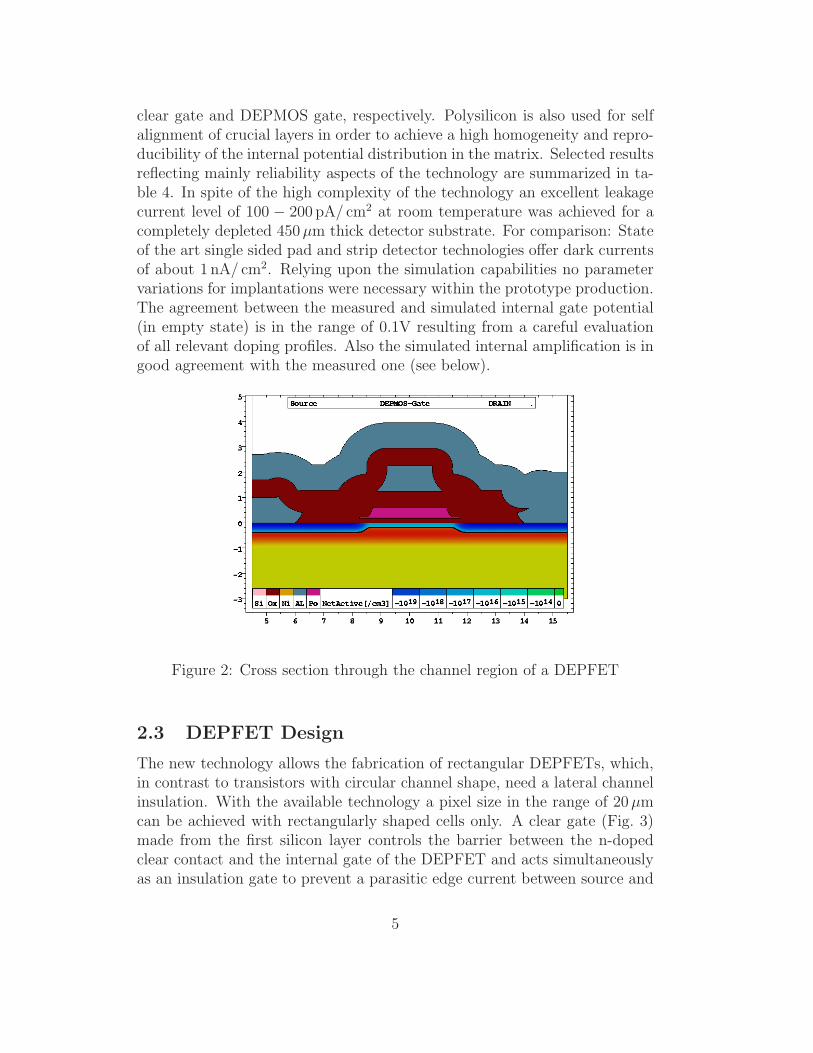
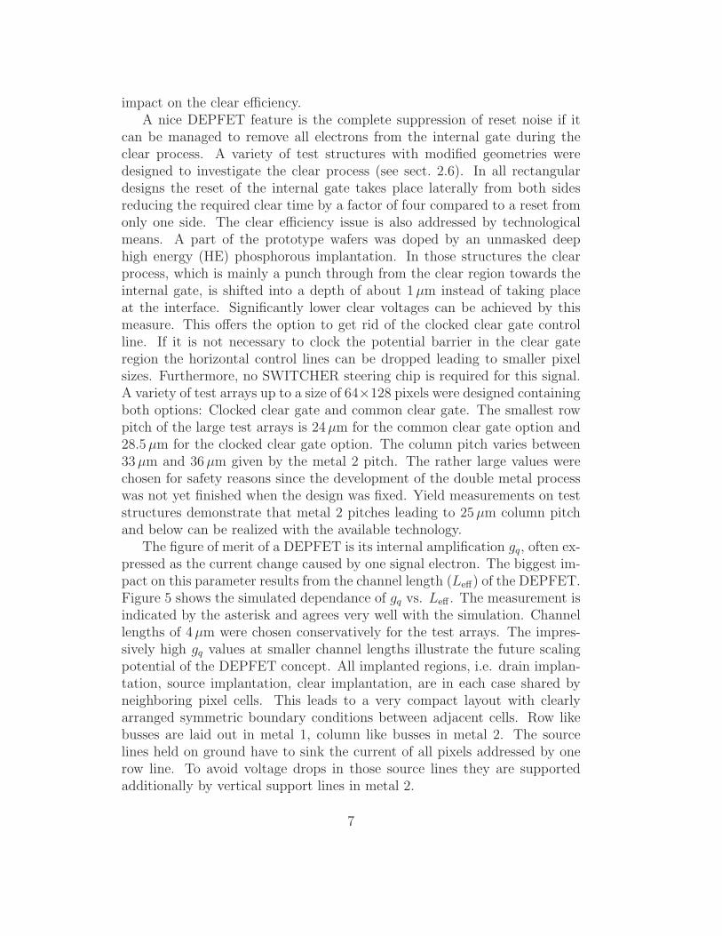
clear gate and DEPMOS gate, respectively. Polysilicon is also used for selfalignment of crucial layers in order to achieve a high homogeneity and repro-ducibility of the internal potential distribution in the matrix. Selected resultsreflecting mainly reliability aspects of the technology are summarized in ta-ble 4. In spite of the high complexity of the technology an excellent leakagecurrent level of 100 − 200 pA/ cm2 at room temperature was achieved for acompletely depleted 450µm thick detector substrate. For comparison: Stateof the art single sided pad and strip detector technologies offer dark currentsof about 1 nA/ cm2. Relying upon the simulation capabilities no parametervariations for implantations were necessary within the prototype production.The agreement between the measured and simulated internal gate potential(in empty state) is in the range of 0.1V resulting from a careful evaluationof all relevant doping profiles. Also the simulated internal amplification is ingood agreement with the measured one (see below).
Figure 2: Cross section through the channel region of a DEPFET
2.3 DEPFET Design
The new technology allows the fabrication of rectangular DEPFETs, which,in contrast to transistors with circular channel shape, need a lateral channelinsulation. With the available technology a pixel size in the range of 20µmcan be achieved with rectangularly shaped cells only. A clear gate (Fig. 3)made from the first silicon layer controls the barrier between the n-dopedclear contact and the internal gate of the DEPFET and acts simultaneouslyas an insulation gate to prevent a parasitic edge current between source and
5
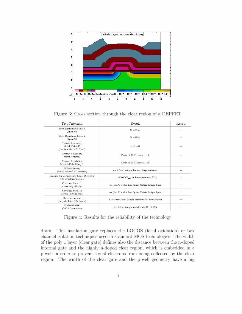
Figure 3: Cross section through the clear region of a DEPFET
Figure 4: Results for the reliability of the technology
drain. This insulation gate replaces the LOCOS (local oxidation) or boxchannel isolation techniques used in standard MOS technologies. The widthof the poly 1 layer (clear gate) defines also the distance between the n-dopedinternal gate and the highly n-doped clear region, which is embedded in ap-well in order to prevent signal electrons from being collected by the clearregion. The width of the clear gate and the p-well geometry have a big
6
impact on the clear efficiency.A nice DEPFET feature is the complete suppression of reset noise if it
can be managed to remove all electrons from the internal gate during theclear process. A variety of test structures with modified geometries weredesigned to investigate the clear process (see sect. 2.6). In all rectangulardesigns the reset of the internal gate takes place laterally from both sidesreducing the required clear time by a factor of four compared to a reset fromonly one side. The clear efficiency issue is also addressed by technologicalmeans. A part of the prototype wafers was doped by an unmasked deephigh energy (HE) phosphorous implantation. In those structures the clearprocess, which is mainly a punch through from the clear region towards theinternal gate, is shifted into a depth of about 1µm instead of taking placeat the interface. Significantly lower clear voltages can be achieved by thismeasure. This offers the option to get rid of the clocked clear gate controlline. If it is not necessary to clock the potential barrier in the clear gateregion the horizontal control lines can be dropped leading to smaller pixelsizes. Furthermore, no SWITCHER steering chip is required for this signal.A variety of test arrays up to a size of 64×128 pixels were designed containingboth options: Clocked clear gate and common clear gate. The smallest rowpitch of the large test arrays is 24µm for the common clear gate option and28.5 µm for the clocked clear gate option. The column pitch varies between33 µm and 36 µm given by the metal 2 pitch. The rather large values werechosen for safety reasons since the development of the double metal processwas not yet finished when the design was fixed. Yield measurements on teststructures demonstrate that metal 2 pitches leading to 25µm column pitchand below can be realized with the available technology.
The figure of merit of a DEPFET is its internal amplification gq, often ex-pressed as the current change caused by one signal electron. The biggest im-pact on this parameter results from the channel length (Leff) of the DEPFET.Figure 5 shows the simulated dependance of gq vs. Leff . The measurement isindicated by the asterisk and agrees very well with the simulation. Channellengths of 4 µm were chosen conservatively for the test arrays. The impres-sively high gq values at smaller channel lengths illustrate the future scalingpotential of the DEPFET concept. All implanted regions, i.e. drain implan-tation, source implantation, clear implantation, are in each case shared byneighboring pixel cells. This leads to a very compact layout with clearlyarranged symmetric boundary conditions between adjacent cells. Row likebusses are laid out in metal 1, column like busses in metal 2. The sourcelines held on ground have to sink the current of all pixels addressed by onerow line. To avoid voltage drops in those source lines they are supportedadditionally by vertical support lines in metal 2.
7
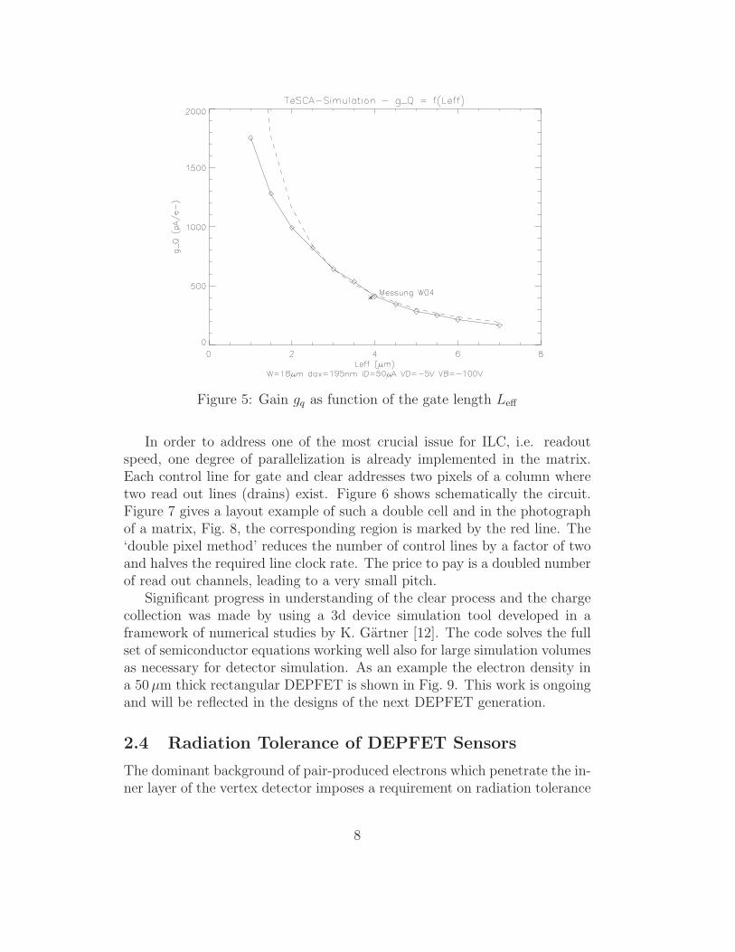
Figure 5: Gain gq as function of the gate length Leff
In order to address one of the most crucial issue for ILC, i.e. readoutspeed, one degree of parallelization is already implemented in the matrix.Each control line for gate and clear addresses two pixels of a column wheretwo read out lines (drains) exist. Figure 6 shows schematically the circuit.Figure 7 gives a layout example of such a double cell and in the photographof a matrix, Fig. 8, the corresponding region is marked by the red line. The‘double pixel method’ reduces the number of control lines by a factor of twoand halves the required line clock rate. The price to pay is a doubled numberof read out channels, leading to a very small pitch.
Significant progress in understanding of the clear process and the chargecollection was made by using a 3d device simulation tool developed in aframework of numerical studies by K. Gartner [12]. The code solves the fullset of semiconductor equations working well also for large simulation volumesas necessary for detector simulation. As an example the electron density ina 50 µm thick rectangular DEPFET is shown in Fig. 9. This work is ongoingand will be reflected in the designs of the next DEPFET generation.
2.4 Radiation Tolerance of DEPFET Sensors
The dominant background of pair-produced electrons which penetrate the in-ner layer of the vertex detector imposes a requirement on radiation tolerance
8
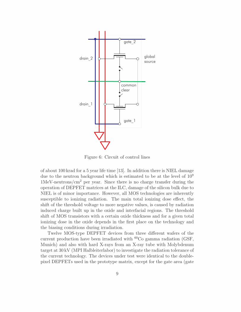
gate_2
gate_1
globalsource
drain_2
drain_1
commonclear
Figure 6: Circuit of control lines
of about 100 krad for a 5 year life time [13]. In addition there is NIEL damagedue to the neutron background which is estimated to be at the level of 109
1MeV-neutrons/cm2 per year. Since there is no charge transfer during theoperation of DEPFET matrices at the ILC, damage of the silicon bulk due toNIEL is of minor importance. However, all MOS technologies are inherentlysusceptible to ionizing radiation. The main total ionizing dose effect, theshift of the threshold voltage to more negative values, is caused by radiationinduced charge built up in the oxide and interfacial regions. The thresholdshift of MOS transistors with a certain oxide thickness and for a given totalionizing dose in the oxide depends in the first place on the technology andthe biasing conditions during irradiation.
Twelve MOS-type DEPFET devices from three different wafers of thecurrent production have been irradiated with 60Co gamma radiation (GSF,Munich) and also with hard X-rays from an X-ray tube with Molybdenumtarget at 30 kV (MPI Halbleiterlabor) to investigate the radiation tolerance ofthe current technology. The devices under test were identical to the double-pixel DEPFETs used in the prototype matrix, except for the gate area (gate
9
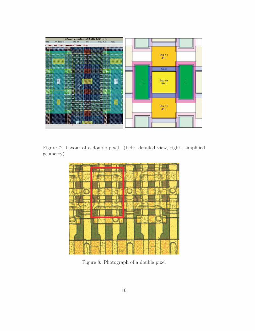
Figure 7: Layout of a double pixel. (Left: detailed view, right: simplifiedgeometry)
Figure 8: Photograph of a double pixel
10
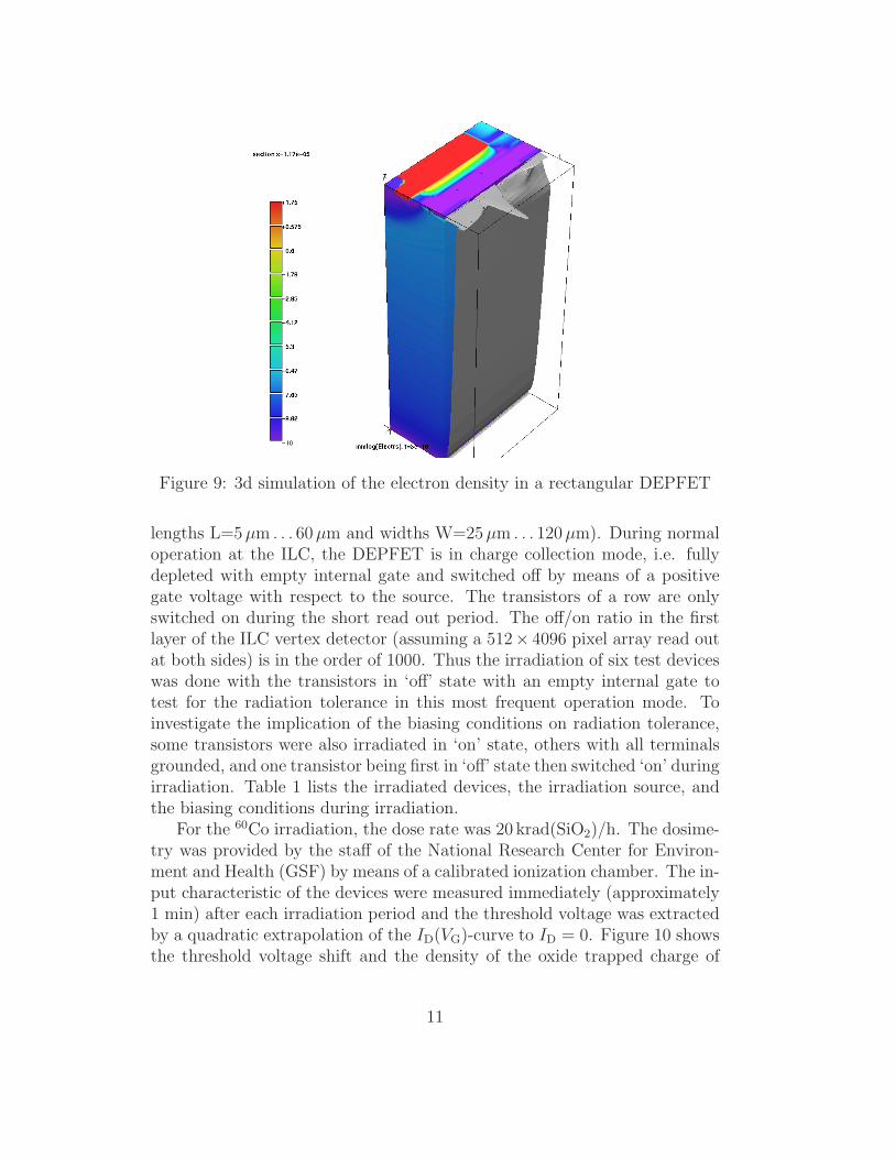
Figure 9: 3d simulation of the electron density in a rectangular DEPFET
lengths L=5µm . . . 60 µm and widths W=25µm . . . 120 µm). During normaloperation at the ILC, the DEPFET is in charge collection mode, i.e. fullydepleted with empty internal gate and switched off by means of a positivegate voltage with respect to the source. The transistors of a row are onlyswitched on during the short read out period. The off/on ratio in the firstlayer of the ILC vertex detector (assuming a 512× 4096 pixel array read outat both sides) is in the order of 1000. Thus the irradiation of six test deviceswas done with the transistors in ‘off’ state with an empty internal gate totest for the radiation tolerance in this most frequent operation mode. Toinvestigate the implication of the biasing conditions on radiation tolerance,some transistors were also irradiated in ‘on’ state, others with all terminalsgrounded, and one transistor being first in ‘off’ state then switched ‘on’ duringirradiation. Table 1 lists the irradiated devices, the irradiation source, andthe biasing conditions during irradiation.
For the 60Co irradiation, the dose rate was 20 krad(SiO2)/h. The dosime-try was provided by the staff of the National Research Center for Environ-ment and Health (GSF) by means of a calibrated ionization chamber. The in-put characteristic of the devices were measured immediately (approximately1 min) after each irradiation period and the threshold voltage was extractedby a quadratic extrapolation of the ID(VG)-curve to ID = 0. Figure 10 showsthe threshold voltage shift and the density of the oxide trapped charge of
11
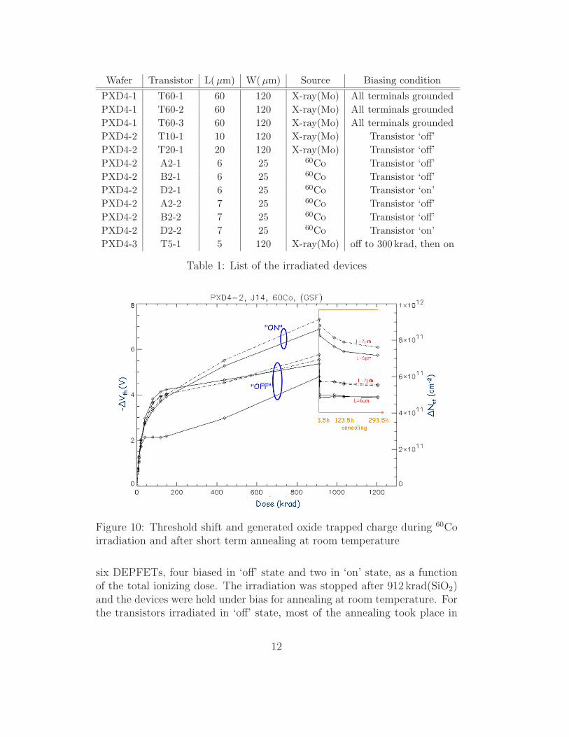
Wafer Transistor L(µm) W(µm) Source Biasing condition
PXD4-1 T60-1 60 120 X-ray(Mo) All terminals grounded
PXD4-1 T60-2 60 120 X-ray(Mo) All terminals grounded
PXD4-1 T60-3 60 120 X-ray(Mo) All terminals grounded
PXD4-2 T10-1 10 120 X-ray(Mo) Transistor ‘off’
PXD4-2 T20-1 20 120 X-ray(Mo) Transistor ‘off’
PXD4-2 A2-1 6 25 60Co Transistor ‘off’
PXD4-2 B2-1 6 25 60Co Transistor ‘off’
PXD4-2 D2-1 6 25 60Co Transistor ‘on’
PXD4-2 A2-2 7 25 60Co Transistor ‘off’
PXD4-2 B2-2 7 25 60Co Transistor ‘off’
PXD4-2 D2-2 7 25 60Co Transistor ‘on’
PXD4-3 T5-1 5 120 X-ray(Mo) off to 300 krad, then on
Table 1: List of the irradiated devices
Figure 10: Threshold shift and generated oxide trapped charge during 60Coirradiation and after short term annealing at room temperature
six DEPFETs, four biased in ‘off’ state and two in ‘on’ state, as a functionof the total ionizing dose. The irradiation was stopped after 912 krad(SiO2)and the devices were held under bias for annealing at room temperature. Forthe transistors irradiated in ‘off’ state, most of the annealing took place in
12
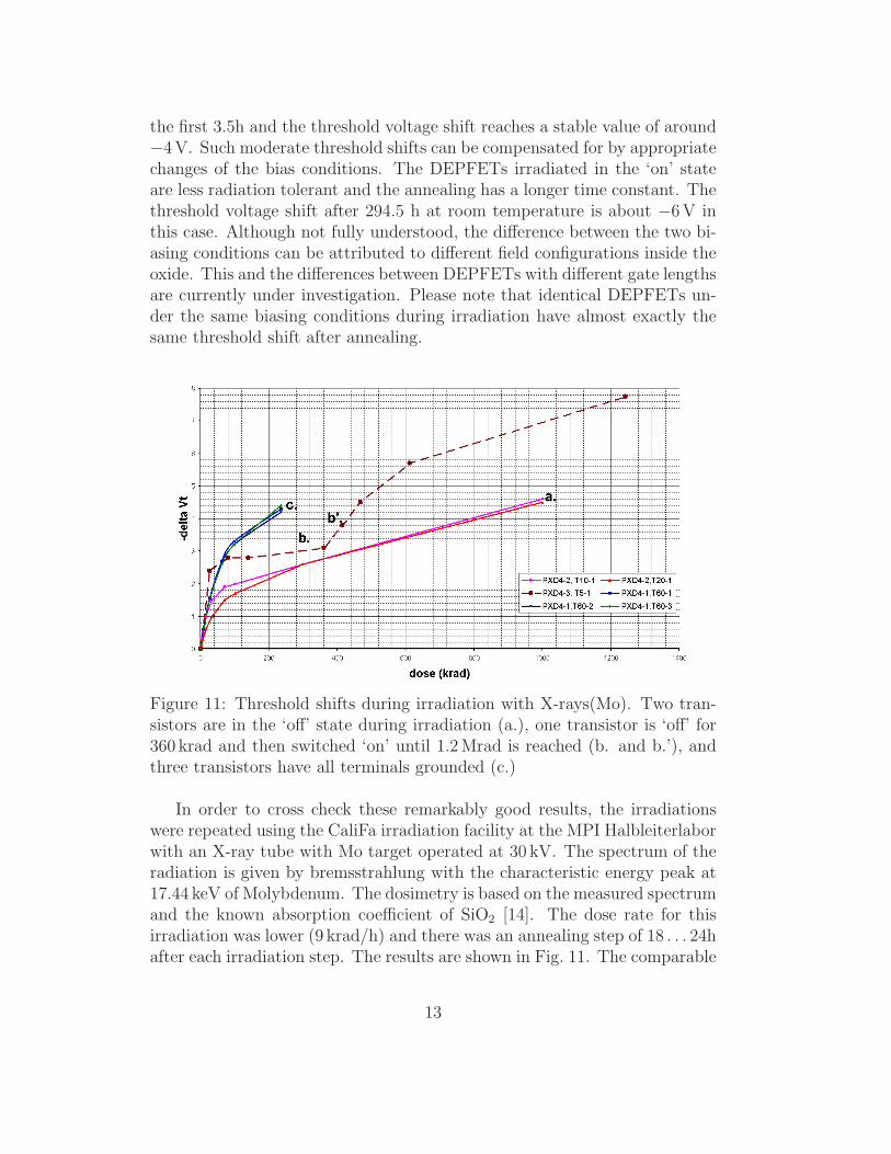
the first 3.5h and the threshold voltage shift reaches a stable value of around−4 V. Such moderate threshold shifts can be compensated for by appropriatechanges of the bias conditions. The DEPFETs irradiated in the ‘on’ stateare less radiation tolerant and the annealing has a longer time constant. Thethreshold voltage shift after 294.5 h at room temperature is about −6 V inthis case. Although not fully understood, the difference between the two bi-asing conditions can be attributed to different field configurations inside theoxide. This and the differences between DEPFETs with different gate lengthsare currently under investigation. Please note that identical DEPFETs un-der the same biasing conditions during irradiation have almost exactly thesame threshold shift after annealing.
Figure 11: Threshold shifts during irradiation with X-rays(Mo). Two tran-sistors are in the ‘off’ state during irradiation (a.), one transistor is ‘off’ for360 krad and then switched ‘on’ until 1.2 Mrad is reached (b. and b.’), andthree transistors have all terminals grounded (c.)
In order to cross check these remarkably good results, the irradiationswere repeated using the CaliFa irradiation facility at the MPI Halbleiterlaborwith an X-ray tube with Mo target operated at 30 kV. The spectrum of theradiation is given by bremsstrahlung with the characteristic energy peak at17.44 keV of Molybdenum. The dosimetry is based on the measured spectrumand the known absorption coefficient of SiO2 [14]. The dose rate for thisirradiation was lower (9 krad/h) and there was an annealing step of 18 . . . 24hafter each irradiation step. The results are shown in Fig. 11. The comparable
13
devices, biased in the same way (curve a. in the figure), show about the samethreshold shift as in the previous irradiation.
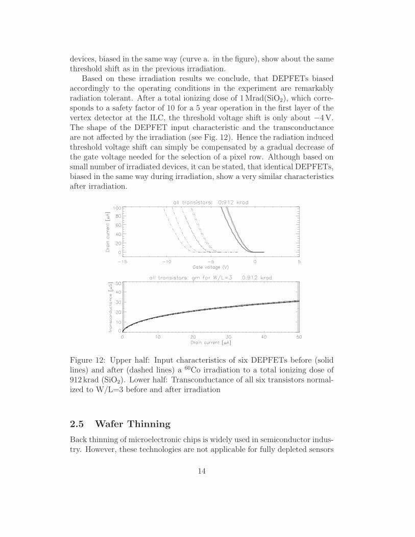
Based on these irradiation results we conclude, that DEPFETs biasedaccordingly to the operating conditions in the experiment are remarkablyradiation tolerant. After a total ionizing dose of 1 Mrad(SiO2), which corre-sponds to a safety factor of 10 for a 5 year operation in the first layer of thevertex detector at the ILC, the threshold voltage shift is only about −4 V.The shape of the DEPFET input characteristic and the transconductanceare not affected by the irradiation (see Fig. 12). Hence the radiation inducedthreshold voltage shift can simply be compensated by a gradual decrease ofthe gate voltage needed for the selection of a pixel row. Although based onsmall number of irradiated devices, it can be stated, that identical DEPFETs,biased in the same way during irradiation, show a very similar characteristicsafter irradiation.
Figure 12: Upper half: Input characteristics of six DEPFETs before (solidlines) and after (dashed lines) a 60Co irradiation to a total ionizing dose of912 krad (SiO2). Lower half: Transconductance of all six transistors normal-ized to W/L=3 before and after irradiation
2.5 Wafer Thinning
Back thinning of microelectronic chips is widely used in semiconductor indus-try. However, these technologies are not applicable for fully depleted sensors
14
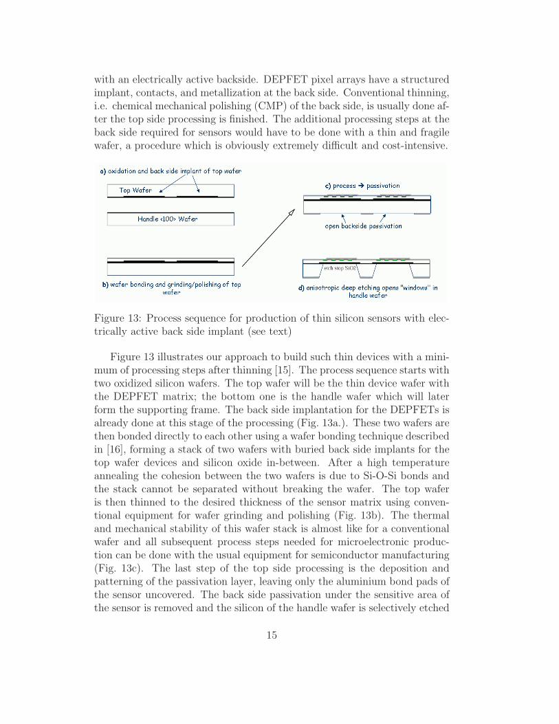
with an electrically active backside. DEPFET pixel arrays have a structuredimplant, contacts, and metallization at the back side. Conventional thinning,i.e. chemical mechanical polishing (CMP) of the back side, is usually done af-ter the top side processing is finished. The additional processing steps at theback side required for sensors would have to be done with a thin and fragilewafer, a procedure which is obviously extremely difficult and cost-intensive.
Figure 13: Process sequence for production of thin silicon sensors with elec-trically active back side implant (see text)
Figure 13 illustrates our approach to build such thin devices with a mini-mum of processing steps after thinning [15]. The process sequence starts withtwo oxidized silicon wafers. The top wafer will be the thin device wafer withthe DEPFET matrix; the bottom one is the handle wafer which will laterform the supporting frame. The back side implantation for the DEPFETs isalready done at this stage of the processing (Fig. 13a.). These two wafers arethen bonded directly to each other using a wafer bonding technique describedin [16], forming a stack of two wafers with buried back side implants for thetop wafer devices and silicon oxide in-between. After a high temperatureannealing the cohesion between the two wafers is due to Si-O-Si bonds andthe stack cannot be separated without breaking the wafer. The top waferis then thinned to the desired thickness of the sensor matrix using conven-tional equipment for wafer grinding and polishing (Fig. 13b). The thermaland mechanical stability of this wafer stack is almost like for a conventionalwafer and all subsequent process steps needed for microelectronic produc-tion can be done with the usual equipment for semiconductor manufacturing(Fig. 13c). The last step of the top side processing is the deposition andpatterning of the passivation layer, leaving only the aluminium bond pads ofthe sensor uncovered. The back side passivation under the sensitive area ofthe sensor is removed and the silicon of the handle wafer is selectively etched
15
away (Fig. 13d). The passivation layer protects the top wafer and serves asthe etch mask for the deep etching of the handle wafer from the back side.The etch process stops after 7 to 9 hours when the handle wafer is etchedthrough and the etch solution reaches the buried SiO2 layer between the topand the handle wafer. The back side implant and the sensitive bulk of thesensor are not affected by the etching process.
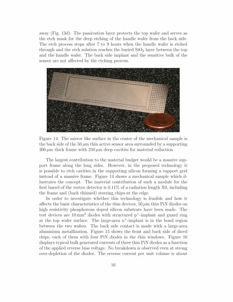
Figure 14: The mirror like surface in the center of the mechanical sample isthe back side of the 50µm thin active sensor area surrounded by a supporting300 µm thick frame with 250µm deep cavities for material reduction
The largest contribution to the material budget would be a massive sup-port frame along the long sides. However, in the proposed technology itis possible to etch cavities in the supporting silicon forming a support gridinstead of a massive frame. Figure 14 shows a mechanical sample which il-lustrates the concept. The material contribution of such a module for thefirst barrel of the vertex detector is 0.11% of a radiation length X0, includingthe frame and (back thinned) steering chips at the edge.
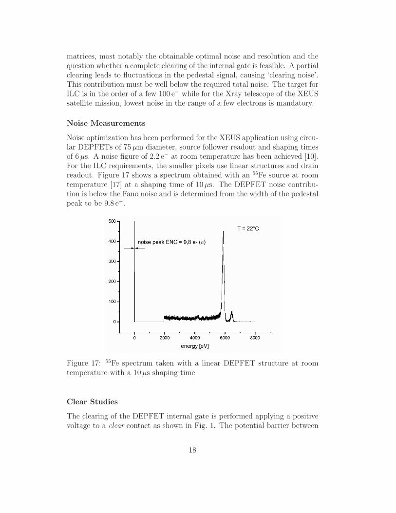
In order to investigate whether this technology is feasible and how itaffects the basic characteristics of the thin devices, 50µm thin PiN diodes onhigh resistivity phosphorous doped silicon substrate have been made. Thetest devices are 10 mm2 diodes with structured p+-implant and guard ringat the top wafer surface. The large-area n+-implant is in the bond regionbetween the two wafers. The back side contact is made with a large-areaaluminium metallization. Figure 15 shows the front and back side of dicedchips, each of them with four PiN diodes in the thin windows. Figure 16displays typical bulk generated currents of three thin PiN diodes as a functionof the applied reverse bias voltage. No breakdown is observed even at strongover-depletion of the diodes. The reverse current per unit volume is about
16
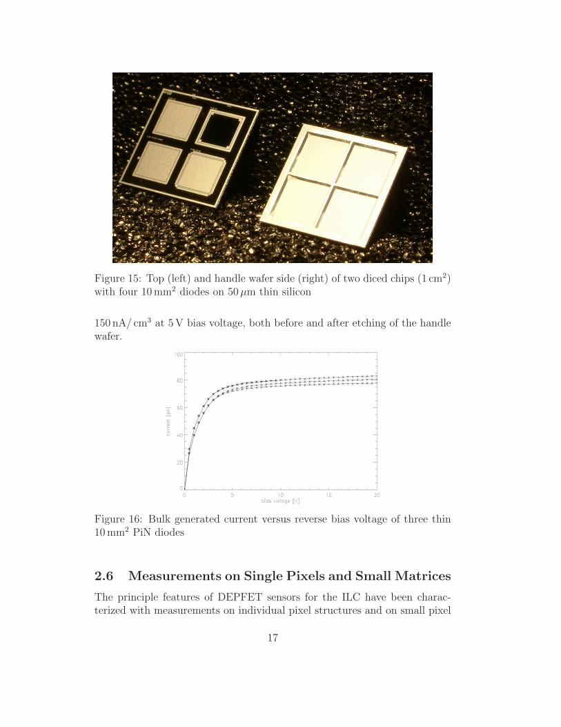
Figure 15: Top (left) and handle wafer side (right) of two diced chips (1 cm2)with four 10 mm2 diodes on 50µm thin silicon
150 nA/ cm3 at 5 V bias voltage, both before and after etching of the handlewafer.
Figure 16: Bulk generated current versus reverse bias voltage of three thin10 mm2 PiN diodes
2.6 Measurements on Single Pixels and Small Matrices
The principle features of DEPFET sensors for the ILC have been charac-terized with measurements on individual pixel structures and on small pixel
17
matrices, most notably the obtainable optimal noise and resolution and thequestion whether a complete clearing of the internal gate is feasible. A partialclearing leads to fluctuations in the pedestal signal, causing ‘clearing noise’.This contribution must be well below the required total noise. The target forILC is in the order of a few 100 e− while for the Xray telescope of the XEUSsatellite mission, lowest noise in the range of a few electrons is mandatory.
Noise Measurements
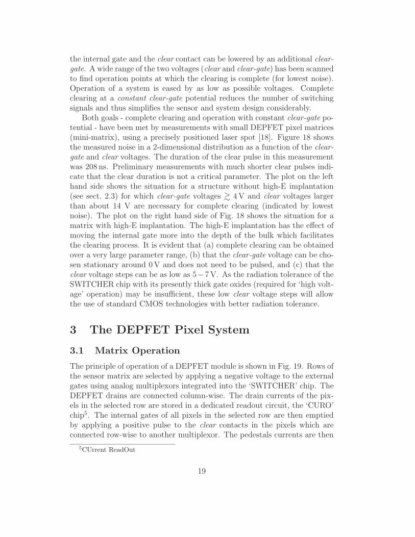
Noise optimization has been performed for the XEUS application using circu-lar DEPFETs of 75 µm diameter, source follower readout and shaping timesof 6 µs. A noise figure of 2.2 e− at room temperature has been achieved [10].For the ILC requirements, the smaller pixels use linear structures and drainreadout. Figure 17 shows a spectrum obtained with an 55Fe source at roomtemperature [17] at a shaping time of 10µs. The DEPFET noise contribu-tion is below the Fano noise and is determined from the width of the pedestalpeak to be 9.8 e−.
Figure 17: 55Fe spectrum taken with a linear DEPFET structure at roomtemperature with a 10µs shaping time
Clear Studies
The clearing of the DEPFET internal gate is performed applying a positivevoltage to a clear contact as shown in Fig. 1. The potential barrier between
18
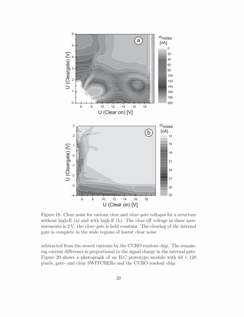
the internal gate and the clear contact can be lowered by an additional clear-gate. A wide range of the two voltages (clear and clear-gate) has been scannedto find operation points at which the clearing is complete (for lowest noise).Operation of a system is eased by as low as possible voltages. Completeclearing at a constant clear-gate potential reduces the number of switchingsignals and thus simplifies the sensor and system design considerably.
Both goals - complete clearing and operation with constant clear-gate po-tential - have been met by measurements with small DEPFET pixel matrices(mini-matrix), using a precisely positioned laser spot [18]. Figure 18 showsthe measured noise in a 2-dimensional distribution as a function of the clear-gate and clear voltages. The duration of the clear pulse in this measurementwas 208 ns. Preliminary measurements with much shorter clear pulses indi-cate that the clear duration is not a critical parameter. The plot on the lefthand side shows the situation for a structure without high-E implantation(see sect. 2.3) for which clear-gate voltages & 4 V and clear voltages largerthan about 14 V are necessary for complete clearing (indicated by lowestnoise). The plot on the right hand side of Fig. 18 shows the situation for amatrix with high-E implantation. The high-E implantation has the effect ofmoving the internal gate more into the depth of the bulk which facilitatesthe clearing process. It is evident that (a) complete clearing can be obtainedover a very large parameter range, (b) that the clear-gate voltage can be cho-sen stationary around 0 V and does not need to be pulsed, and (c) that theclear voltage steps can be as low as 5−7 V. As the radiation tolerance of theSWITCHER chip with its presently thick gate oxides (required for ‘high volt-age’ operation) may be insufficient, these low clear voltage steps will allowthe use of standard CMOS technologies with better radiation tolerance.
3 The DEPFET Pixel System
3.1 Matrix Operation
The principle of operation of a DEPFET module is shown in Fig. 19. Rows ofthe sensor matrix are selected by applying a negative voltage to the externalgates using analog multiplexors integrated into the ‘SWITCHER’ chip. TheDEPFET drains are connected column-wise. The drain currents of the pix-els in the selected row are stored in a dedicated readout circuit, the ‘CURO’chip5. The internal gates of all pixels in the selected row are then emptiedby applying a positive pulse to the clear contacts in the pixels which areconnected row-wise to another multiplexor. The pedestals currents are then
5CUrrent ReadOut
19
6 8 10 12 14 16 18
0
1
2
3
4
5
6
0
20
40
60
80
100
120
140
160
180
200
U (Clear on) [V]
U (
Cle
arg
ate
) [V
]
σnoise[nA]
a
6 8 10 12 14 16 18
-4
-3
-2
-1
0
1
2
3
U (Clear on) [V]
U (
Cle
arg
ate
) [V
]
12
15
18
21
24
27
30
32
σnoise[nA]b
Figure 18: Clear noise for various clear and clear-gate voltages for a structurewithout high-E (a) and with high-E (b). The clear off voltage in these mea-surements is 2 V, the clear-gate is held constant. The clearing of the internalgate is complete in the wide regions of lowest clear noise
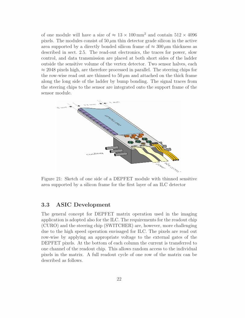
subtracted from the stored currents by the CURO readout chip. The remain-ing current difference is proportional to the signal charge in the internal gate.Figure 20 shows a photograph of an ILC prototype module with 64 × 128pixels, gate- and clear SWITCHERs and the CURO readout chip.
20
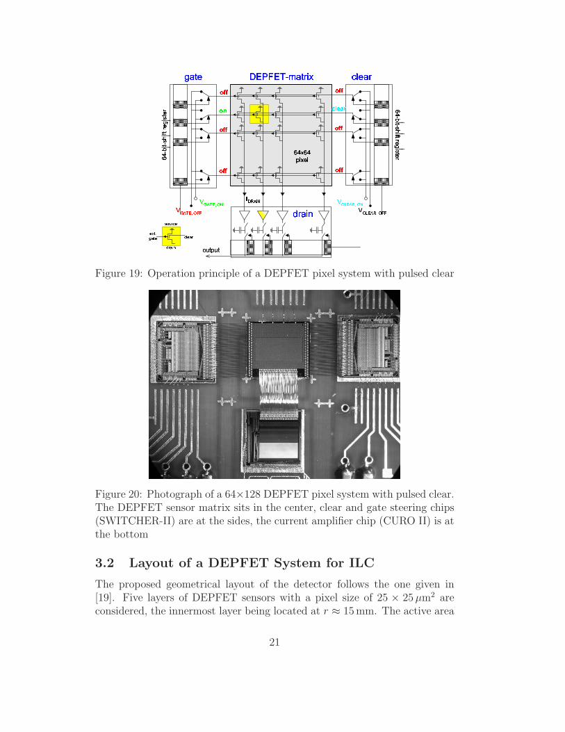
Figure 19: Operation principle of a DEPFET pixel system with pulsed clear
Figure 20: Photograph of a 64×128 DEPFET pixel system with pulsed clear.The DEPFET sensor matrix sits in the center, clear and gate steering chips(SWITCHER-II) are at the sides, the current amplifier chip (CURO II) is atthe bottom
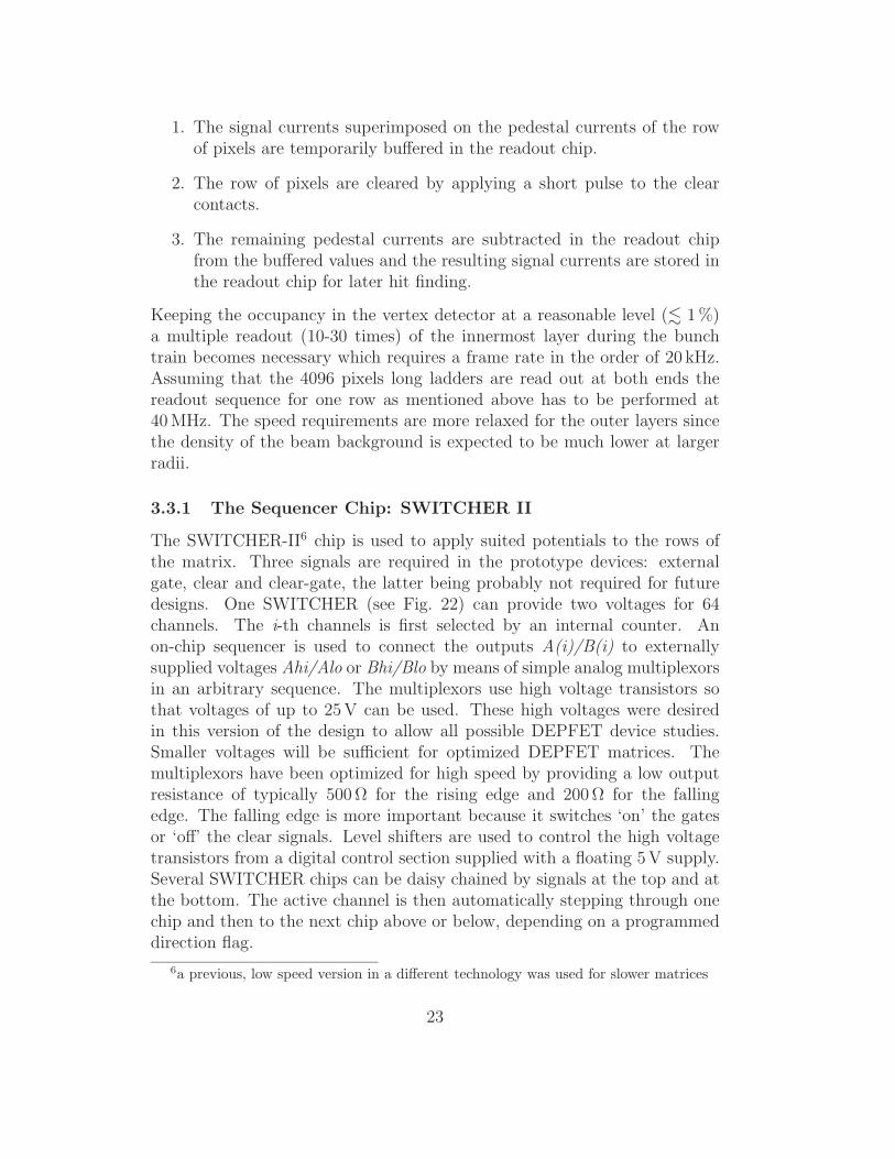
3.2 Layout of a DEPFET System for ILC
The proposed geometrical layout of the detector follows the one given in[19]. Five layers of DEPFET sensors with a pixel size of 25 × 25 µm2 areconsidered, the innermost layer being located at r ≈ 15 mm. The active area
21
of one module will have a size of ≈ 13 × 100 mm2 and contain 512 × 4096pixels. The modules consist of 50 µm thin detector grade silicon in the activearea supported by a directly bonded silicon frame of ≈ 300 µm thickness asdescribed in sect. 2.5. The read-out electronics, the traces for power, slowcontrol, and data transmission are placed at both short sides of the ladderoutside the sensitive volume of the vertex detector. Two sensor halves, each≈ 2048 pixels high, are therefore processed in parallel. The steering chips forthe row-wise read out are thinned to 50µm and attached on the thick framealong the long side of the ladder by bump bonding. The signal traces fromthe steering chips to the sensor are integrated onto the support frame of thesensor module.
Figure 21: Sketch of one side of a DEPFET module with thinned sensitivearea supported by a silicon frame for the first layer of an ILC detector
3.3 ASIC Development
The general concept for DEPFET matrix operation used in the imagingapplication is adopted also for the ILC. The requirements for the readout chip(CURO) and the steering chip (SWITCHER) are, however, more challengingdue to the high speed operation envisaged for ILC. The pixels are read outrow-wise by applying an appropriate voltage to the external gates of theDEPFET pixels. At the bottom of each column the current is transferred toone channel of the readout chip. This allows random access to the individualpixels in the matrix. A full readout cycle of one row of the matrix can bedescribed as follows.
22
1. The signal currents superimposed on the pedestal currents of the rowof pixels are temporarily buffered in the readout chip.
2. The row of pixels are cleared by applying a short pulse to the clearcontacts.
3. The remaining pedestal currents are subtracted in the readout chipfrom the buffered values and the resulting signal currents are stored inthe readout chip for later hit finding.
Keeping the occupancy in the vertex detector at a reasonable level (. 1 %)a multiple readout (10-30 times) of the innermost layer during the bunchtrain becomes necessary which requires a frame rate in the order of 20 kHz.Assuming that the 4096 pixels long ladders are read out at both ends thereadout sequence for one row as mentioned above has to be performed at40 MHz. The speed requirements are more relaxed for the outer layers sincethe density of the beam background is expected to be much lower at largerradii.
3.3.1 The Sequencer Chip: SWITCHER II
The SWITCHER-II6 chip is used to apply suited potentials to the rows ofthe matrix. Three signals are required in the prototype devices: externalgate, clear and clear-gate, the latter being probably not required for futuredesigns. One SWITCHER (see Fig. 22) can provide two voltages for 64channels. The i-th channels is first selected by an internal counter. Anon-chip sequencer is used to connect the outputs A(i)/B(i) to externallysupplied voltages Ahi/Alo or Bhi/Blo by means of simple analog multiplexorsin an arbitrary sequence. The multiplexors use high voltage transistors sothat voltages of up to 25 V can be used. These high voltages were desiredin this version of the design to allow all possible DEPFET device studies.Smaller voltages will be sufficient for optimized DEPFET matrices. Themultiplexors have been optimized for high speed by providing a low outputresistance of typically 500 Ω for the rising edge and 200 Ω for the fallingedge. The falling edge is more important because it switches ‘on’ the gatesor ‘off’ the clear signals. Level shifters are used to control the high voltagetransistors from a digital control section supplied with a floating 5 V supply.Several SWITCHER chips can be daisy chained by signals at the top and atthe bottom. The active channel is then automatically stepping through onechip and then to the next chip above or below, depending on a programmeddirection flag.
6a previous, low speed version in a different technology was used for slower matrices
23
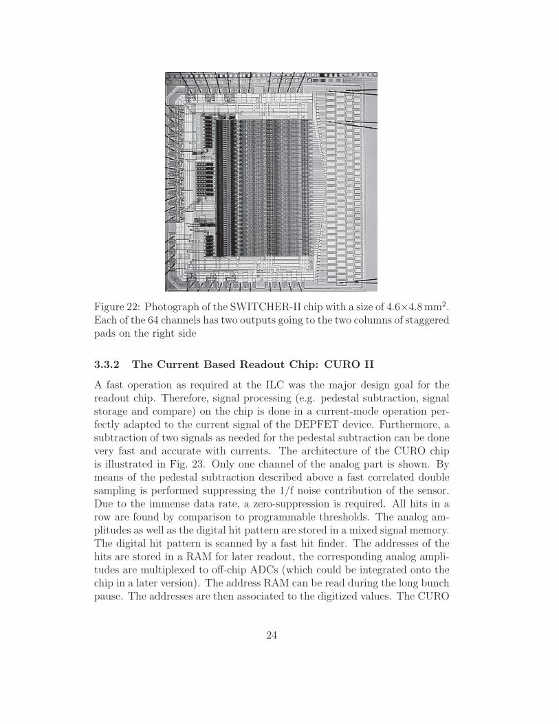
Figure 22: Photograph of the SWITCHER-II chip with a size of 4.6×4.8 mm2.Each of the 64 channels has two outputs going to the two columns of staggeredpads on the right side
3.3.2 The Current Based Readout Chip: CURO II
A fast operation as required at the ILC was the major design goal for thereadout chip. Therefore, signal processing (e.g. pedestal subtraction, signalstorage and compare) on the chip is done in a current-mode operation per-fectly adapted to the current signal of the DEPFET device. Furthermore, asubtraction of two signals as needed for the pedestal subtraction can be donevery fast and accurate with currents. The architecture of the CURO chipis illustrated in Fig. 23. Only one channel of the analog part is shown. Bymeans of the pedestal subtraction described above a fast correlated doublesampling is performed suppressing the 1/f noise contribution of the sensor.Due to the immense data rate, a zero-suppression is required. All hits in arow are found by comparison to programmable thresholds. The analog am-plitudes as well as the digital hit pattern are stored in a mixed signal memory.The digital hit pattern is scanned by a fast hit finder. The addresses of thehits are stored in a RAM for later readout, the corresponding analog ampli-tudes are multiplexed to off-chip ADCs (which could be integrated onto thechip in a later version). The address RAM can be read during the long bunchpause. The addresses are then associated to the digitized values. The CURO
24
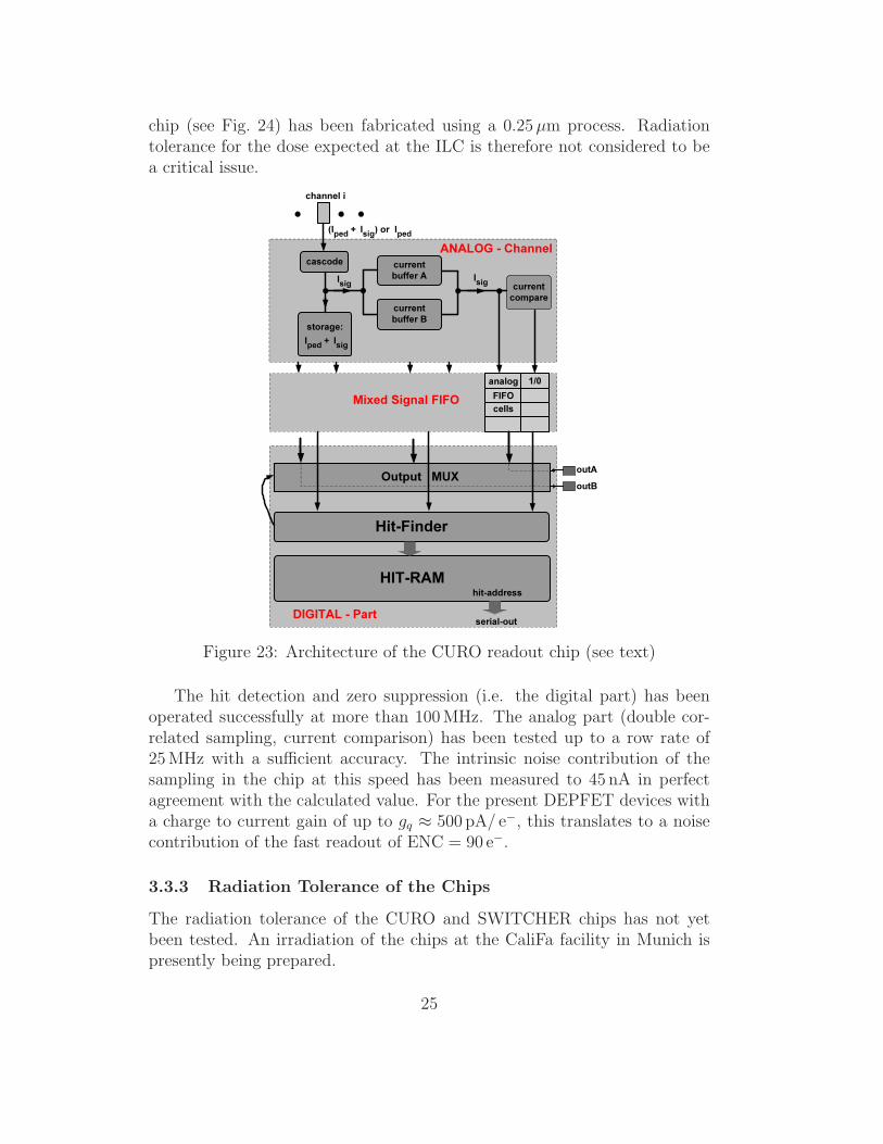
chip (see Fig. 24) has been fabricated using a 0.25 µm process. Radiationtolerance for the dose expected at the ILC is therefore not considered to bea critical issue.
cascode currentbuffer A
currentbuffer B
Hit-Finder
HIT-RAM
storage: Iped + Isig
currentcompare
serial-out
1/0
hit-address
analogFIFOcells
(Iped + Isig) or Iped
IsigIsig
channel i
outAoutB
DIGITAL - Part
ANALOG - Channel
Output MUX
Mixed Signal FIFO
Figure 23: Architecture of the CURO readout chip (see text)
The hit detection and zero suppression (i.e. the digital part) has beenoperated successfully at more than 100 MHz. The analog part (double cor-related sampling, current comparison) has been tested up to a row rate of25 MHz with a sufficient accuracy. The intrinsic noise contribution of thesampling in the chip at this speed has been measured to 45 nA in perfectagreement with the calculated value. For the present DEPFET devices witha charge to current gain of up to gq ≈ 500 pA/ e−, this translates to a noisecontribution of the fast readout of ENC = 90 e−.
3.3.3 Radiation Tolerance of the Chips
The radiation tolerance of the CURO and SWITCHER chips has not yetbeen tested. An irradiation of the chips at the CaliFa facility in Munich ispresently being prepared.
25
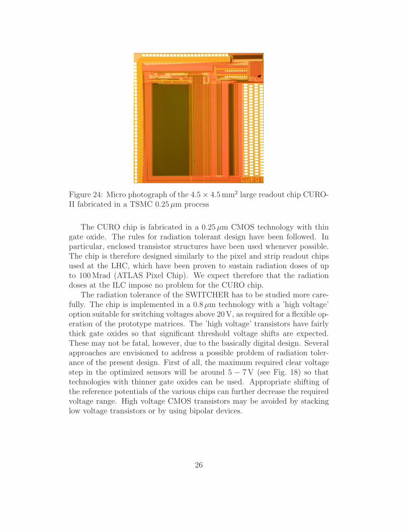
Figure 24: Micro photograph of the 4.5 × 4.5 mm2 large readout chip CURO-II fabricated in a TSMC 0.25 µm process
The CURO chip is fabricated in a 0.25 µm CMOS technology with thingate oxide. The rules for radiation tolerant design have been followed. Inparticular, enclosed transistor structures have been used whenever possible.The chip is therefore designed similarly to the pixel and strip readout chipsused at the LHC, which have been proven to sustain radiation doses of upto 100 Mrad (ATLAS Pixel Chip). We expect therefore that the radiationdoses at the ILC impose no problem for the CURO chip.
The radiation tolerance of the SWITCHER has to be studied more care-fully. The chip is implemented in a 0.8 µm technology with a ’high voltage’option suitable for switching voltages above 20 V, as required for a flexible op-eration of the prototype matrices. The ’high voltage’ transistors have fairlythick gate oxides so that significant threshold voltage shifts are expected.These may not be fatal, however, due to the basically digital design. Severalapproaches are envisioned to address a possible problem of radiation toler-ance of the present design. First of all, the maximum required clear voltagestep in the optimized sensors will be around 5 − 7 V (see Fig. 18) so thattechnologies with thinner gate oxides can be used. Appropriate shifting ofthe reference potentials of the various chips can further decrease the requiredvoltage range. High voltage CMOS transistors may be avoided by stackinglow voltage transistors or by using bipolar devices.
26
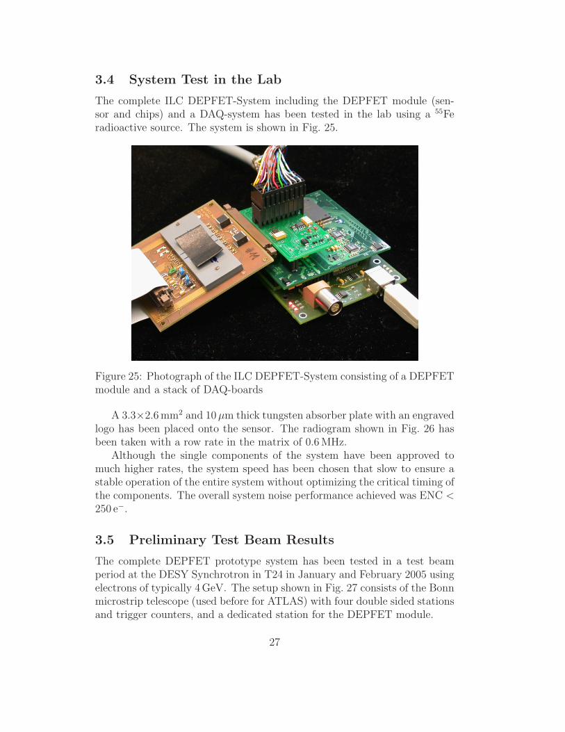
3.4 System Test in the Lab
The complete ILC DEPFET-System including the DEPFET module (sen-sor and chips) and a DAQ-system has been tested in the lab using a 55Feradioactive source. The system is shown in Fig. 25.
Figure 25: Photograph of the ILC DEPFET-System consisting of a DEPFETmodule and a stack of DAQ-boards
A 3.3×2.6 mm2 and 10 µm thick tungsten absorber plate with an engravedlogo has been placed onto the sensor. The radiogram shown in Fig. 26 hasbeen taken with a row rate in the matrix of 0.6 MHz.
Although the single components of the system have been approved tomuch higher rates, the system speed has been chosen that slow to ensure astable operation of the entire system without optimizing the critical timing ofthe components. The overall system noise performance achieved was ENC <250 e−.
3.5 Preliminary Test Beam Results
The complete DEPFET prototype system has been tested in a test beamperiod at the DESY Synchrotron in T24 in January and February 2005 usingelectrons of typically 4 GeV. The setup shown in Fig. 27 consists of the Bonnmicrostrip telescope (used before for ATLAS) with four double sided stationsand trigger counters, and a dedicated station for the DEPFET module.
27
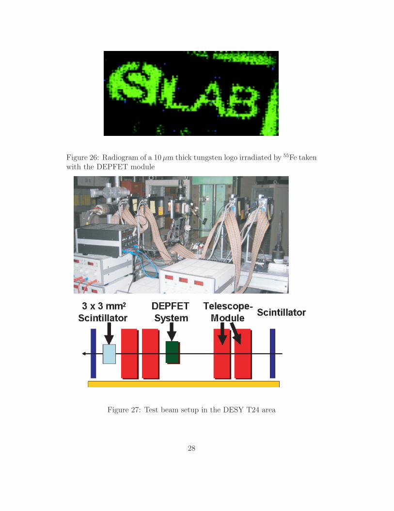
Figure 26: Radiogram of a 10µm thick tungsten logo irradiated by 55Fe takenwith the DEPFET module
Figure 27: Test beam setup in the DESY T24 area
28
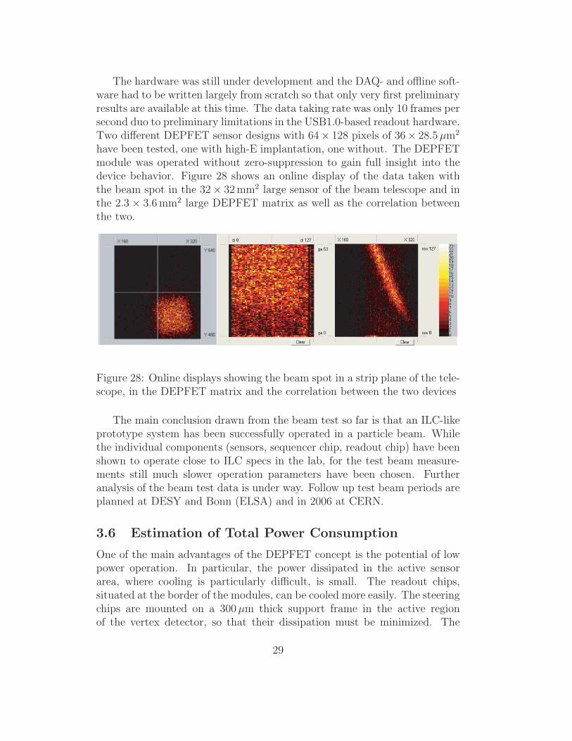
The hardware was still under development and the DAQ- and offline soft-ware had to be written largely from scratch so that only very first preliminaryresults are available at this time. The data taking rate was only 10 frames persecond duo to preliminary limitations in the USB1.0-based readout hardware.Two different DEPFET sensor designs with 64× 128 pixels of 36× 28.5 µm2
have been tested, one with high-E implantation, one without. The DEPFETmodule was operated without zero-suppression to gain full insight into thedevice behavior. Figure 28 shows an online display of the data taken withthe beam spot in the 32× 32 mm2 large sensor of the beam telescope and inthe 2.3 × 3.6 mm2 large DEPFET matrix as well as the correlation betweenthe two.
Figure 28: Online displays showing the beam spot in a strip plane of the tele-scope, in the DEPFET matrix and the correlation between the two devices
The main conclusion drawn from the beam test so far is that an ILC-likeprototype system has been successfully operated in a particle beam. Whilethe individual components (sensors, sequencer chip, readout chip) have beenshown to operate close to ILC specs in the lab, for the test beam measure-ments still much slower operation parameters have been chosen. Furtheranalysis of the beam test data is under way. Follow up test beam periods areplanned at DESY and Bonn (ELSA) and in 2006 at CERN.
3.6 Estimation of Total Power Consumption
One of the main advantages of the DEPFET concept is the potential of lowpower operation. In particular, the power dissipated in the active sensorarea, where cooling is particularly difficult, is small. The readout chips,situated at the border of the modules, can be cooled more easily. The steeringchips are mounted on a 300µm thick support frame in the active regionof the vertex detector, so that their dissipation must be minimized. The
29
power consumption of the sensor can be estimated assuming VDrain=5 V andIdrain = 100µA (these are conservative values) corresponding to 500µW peractive DEPFET. The total number of pixels active at the same time in theinnermost layer 1 is 8192, located in 16 rows (2 on each of the 8 ladders)with 512 pixels each. The power dissipation during readout is thus 4.1 W.The duty cycle of ≈ 1/200 given by the bunch structure at ILC reduces thispeak value to an average sensor power dissipation of only 20 mW for the firstlayer. The power dissipated by the present SWITCHER and CURO chipshas been measured. The SWITCHER dissipates 6.3 mW per channel at thetarget row rate of 50 MHz. The CURO requires 2.8 mW per channel, out ofwhich ≈ 400 µW are used in the input stage. This fraction may have to beincreased somewhat for larger matrices. Scaling these values to the numberof pixels in the innermost layer leads to a peak consumption of 0.1 W for theSWITCHER and 23 W for the CURO or an average consumption of 115 mWfor the innermost layer, dominated by the CURO chip. Note that the CUROchips are situated outside of the active area and can thus be cooled moreeasily. This calculation assumes that the dissipation of the chips in thebeam gaps is made negligible by appropriate circuit design. This will be arequirement for future chip versions. Scaling up the average dissipation of115 mW+20 mW for the 18.7 Mpixels of the first layer to the full area of the5 layers with ≈ 493 Mpixels leads to a total average dissipation of 4 W.
4 Summary
We believe that most R&D goals expressed in the PRC 2003 have successfullybeen met:
⊲ the thinning technology has been demonstrated
⊲ prototype DEPFET matrices with close-to-ILC pixel sizes can be op-erated with low noise and complete clear
⊲ the radiation tolerance of the sensors up to 1 Mrad has been demon-strated. This is well above the requirement of at most 200 krad forILC
⊲ prototype readout and steering chips are close to ILC specifications
⊲ a prototype module and system demonstrator with 64 × 128 pixelsincluding all system components has been built and has been operatedsuccessfully in a test beam.
These encouraging results make us confident that we will be able to go tothe next step of a system closer to ILC specs with respect to size (close to
30
full size module), thickness and readout speed.
4.1 Further Planning
The next steps planned are:
⊲ test of radiation tolerance of the chips and of a complete system
⊲ carry out a second test beam at ELSA (Bonn) with further optimizationof the operation parameters
⊲ carry out a third test beam at CERN with high energetic particles tostudy spatial resolution
⊲ determine the limits of the readout speed of the present system
⊲ design a new generation of readout chips adapted to the known param-eters of the favored (high-E) matrices
⊲ prepare for the construction of a 512×512 close to full size system withmultiple readout chips
The DEPFET collaboration at present consists of the groups from BonnUniversity (N. Wermes et al.), Mannheim University (P. Fischer et al.) andfrom MPI/MPE Munich Halbleiterlabor (H. G. Moser, L. Struder et al.).We are in the process to increase the collaboration for focussed R&D for theILC. Groups from Prague (Z. Dolezal et al.) and Cracow (W. Kucewicz)have expressed interest.
References
[1] J. Kemmer, G. Lutz: New semiconductor detector concepts. Nucl.Inst. & Meth. A253 356 (1987)
[2] J. Kemmer, G. Lutz et al.: Experimental confirmation of a newsemiconductor detector principle. Nucl. Inst. & Meth. A288 92(1990)
[3] P. Klein et al.: Study of a DEPJFET pixel matrix with continuousclear mechanism. Nucl. Inst. & Meth. A392 254 (1997)
[4] P. Fischer et al.: First operation of a pixel imaging matrix basedon DEPFET pixels. Nucl. Inst. & Meth. A451 651 (2000)
[5] W. Neeser et al.: The DEPFET Pixel BIOSCOPE. IEEE Trans.Nucl. Sci. 47 No.3 (2000).
31
[6] J. Ulrici et al.: Spectroscopic and imaging performance of DEP-FET pixel sensors. Nucl. Inst. & Meth. A465 247-252 (2001).
[7] J. Ulrici et al.: Imaging Performance of a DEPFET pixel Bioscopesystem in Tritium autoradiography. Submitted to NIM (2003)
[8] E. Gatti, P. Rehak: Semiconductor drift chamber - An applicationof a novel charge transport scheme. Nucl. Inst. & Meth. A225 608(1984)
[9] G. Cesura et al.: New pixel detector concepts based on junctionfield effect transitors on high resistivity silicon. Nucl. Inst. & Meth.A377 521 (1996)
[10] M. Porro et al. Spectroscopic Performances of DePMOS Detec-tor/Amplifier Device with Respect to Different Filtering Tech-niques and Operating Conditions. Submitted to IEEE TNS, Rome,(November 2004)
[11] ISE TCAD Realease 7.0 V01.2b, DIOS 2001
[12] H. Gajewski et al., TESCA - Two Dimensional SemiconductorAnalysis Package, Handbuch, WIAS, Berlin, 1997
[13] T. Behnke, S. Bertolucci, R. D. Heuer and R. Settles: TESLA: Thesuperconducting electron positron linear collider with an integratedX-ray laser laboratory. Technical design report. Pt. 4: A detectorfor TESLA’, DESY-01-011.
[14] A. Pahlke: Einfluss der Oxidqualitat auf die Stabilitat von Halblei-terdetektoren bei Rontgenstrahlung, Phd. Thesis, TU Muenchen,2003
[15] L. Andricek et al.: Processing of ultra-thin silicon sensors forfuture e+e− linear collider experiments, IEEE Trans. Nucl. Sci.51 No. 3, pp. 1117–1120 (2004).
[16] Q. Y. Tong, U. Goesele: Semiconductor Wafer Bonding, John Wi-ley & Sons, New York, 1999.
[17] R. Kohrs et al. Development of a prototype module for a DEPFETpixel vertex detector for a linear collider. Submitted to IEEE TNS,Rome (November 2004)
32

[18] C. Sandow: Ladungssammlung und Loschvorgang von DEPFETPixelsensoren. Diploma Thesis, Bonn University, (April 2005)
[19] P. Fischer et al.: DESY PRC report 4/2003
33