Embed Size (px)
DESCRIPTION
This paper presents low area and power efficient delay register using CMOS transistors. The proposed register has reduced area than the conventional register. This resistor design consists of 6 NMOS and 6 PMOS. The proposed delay register has been designed in logic editor and simulated using 90nm technology. Also the layout simulation and parametric analysis has been done to find out the results. In this paper register has been designed using full automatic layout design and semicustom layout design. Then the performance of these different designs has been analyzed and compared in terms of power, delay and area. The simulation result shows that circuit design of delay register using PTL techniques improved by power 0.05% and 61.8% area.
Citation preview
Int. Journal of Electrical & Electronics Engg. Vol. 2, Spl. Issue 1 (2015) e-ISSN: 1694-2310 | p-ISSN: 1694-2426
63 NITTTR, Chandigarh EDIT-2015
Design Analysis of Delay Register with PTLLogic using 90 nm Technology
Meenakshi ThakurDepartment of ECE, National Institute of Technical Teacher’s Training & Research Chandigarh, India
Abstract: This paper presents low area and power efficientdelay register using CMOS transistors. The proposed registerhas reduced area than the conventional register. This resistordesign consists of 6 NMOS and 6 PMOS. The proposed delayregister has been designed in logic editor and simulated using90nm technology. Also the layout simulation and parametricanalysis has been done to find out the results. In this paperregister has been designed using full automatic layout designand semicustom layout design. Then the performance of thesedifferent designs has been analyzed and compared in terms ofpower, delay and area. The simulation result shows that circuitdesign of delay register using PTL techniques improved bypower 0.05% and 61.8% area.
Keywords: CMOS, Power Dissipation, NMOS, PMOS, PassTransistor.
1. INTRODUCTIONFlip flops are the circuit used in shift registers, for storageof bits, amplifiers, counters and synchronizer applications.The demand of miniature and transferable accessories israising fast with the time. So designer has to kept in mindthe various features like silicon area, longer life , high speed,reliability and weight of the device. Also battery and areaconsumption is limitation of many portable devices. Thesophistication of the device can be increased by using theproper CMOS designs. So a lot of logical style have beendeveloped to improve the power consumption and area,delays are also minimized [1-2].In order to reduce heatdissipation and power consumption it is required to reducethe supply voltage, switching frequency and capacitance oftransistor [3].The total power dissipation in cmos circuit isthe some of static power dissipation, short circuit dissipationand dynamic power dissipation.
Ptotal = Ps+Pd+Psc (1)
Also to get optimized time domain performance it isrequired to adjust transistor dimensions individually[4-5].Edge-triggered flip flops are used where delays match theadequate clock period, by changing the time of activation ofregisters the throughput of the circuit can bemaximized[6].The D input must be held stable until theoutput Q appears. Also in order to increase the efficiency ofthe circuit double edge triggered flip flops can also be used[7]. Edge triggered register ensures that the result is writtenin instant and then the input close, and allow the system toperform its operation in orderly and stable way.
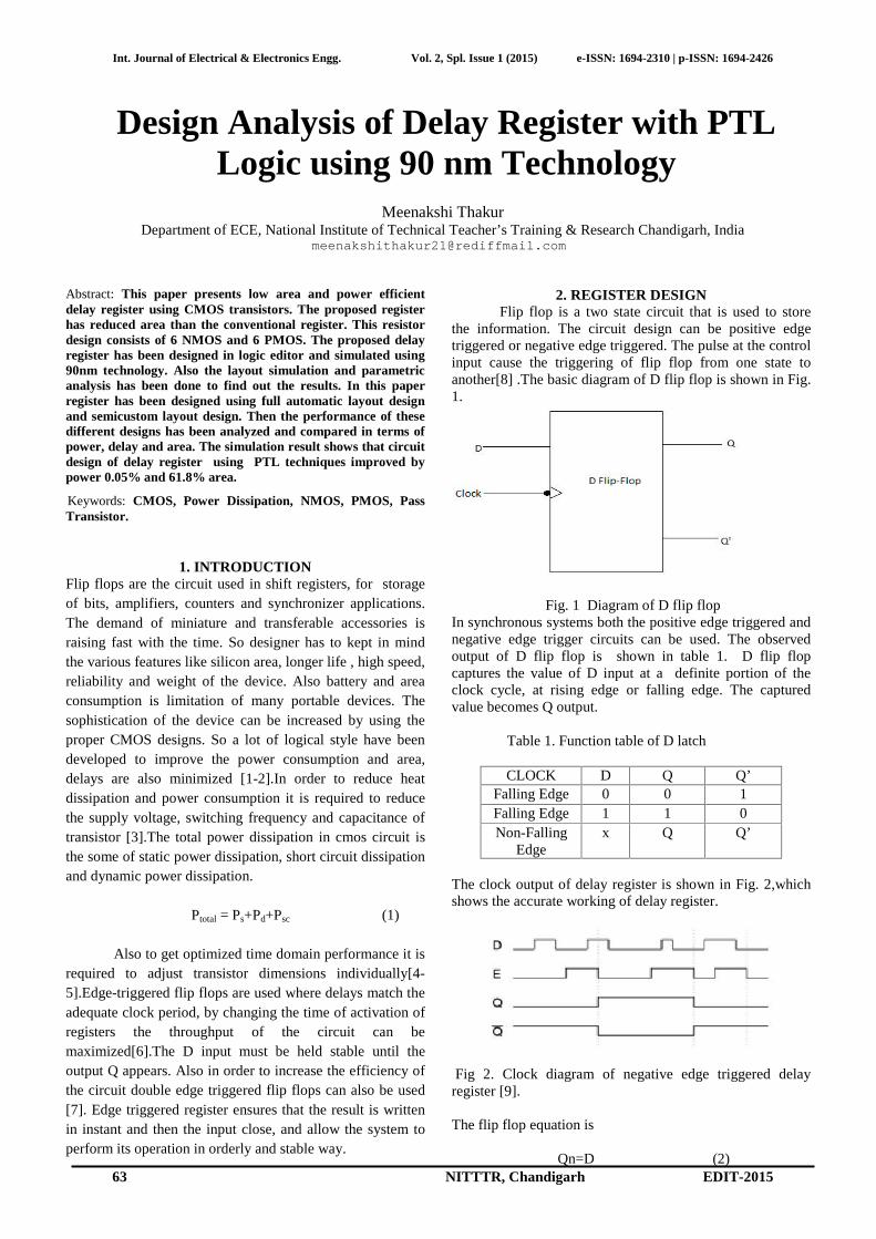
2. REGISTER DESIGNFlip flop is a two state circuit that is used to store
the information. The circuit design can be positive edgetriggered or negative edge triggered. The pulse at the controlinput cause the triggering of flip flop from one state toanother[8] .The basic diagram of D flip flop is shown in Fig.1.
Fig. 1 Diagram of D flip flopIn synchronous systems both the positive edge triggered andnegative edge trigger circuits can be used. The observedoutput of D flip flop is shown in table 1. D flip flopcaptures the value of D input at a definite portion of theclock cycle, at rising edge or falling edge. The capturedvalue becomes Q output.
Table 1. Function table of D latch
CLOCK D Q Q’Falling Edge 0 0 1Falling Edge 1 1 0Non-Falling
Edgex Q Q’
The clock output of delay register is shown in Fig. 2,whichshows the accurate working of delay register.
Fig 2. Clock diagram of negative edge triggered delayregister [9].
The flip flop equation is
Qn=D (2)
Int. Journal of Electrical & Electronics Engg. Vol. 2, Spl. Issue 1 (2015) e-ISSN: 1694-2310 | p-ISSN: 1694-2426
NITTTR, Chandigarh EDIT -2015 64
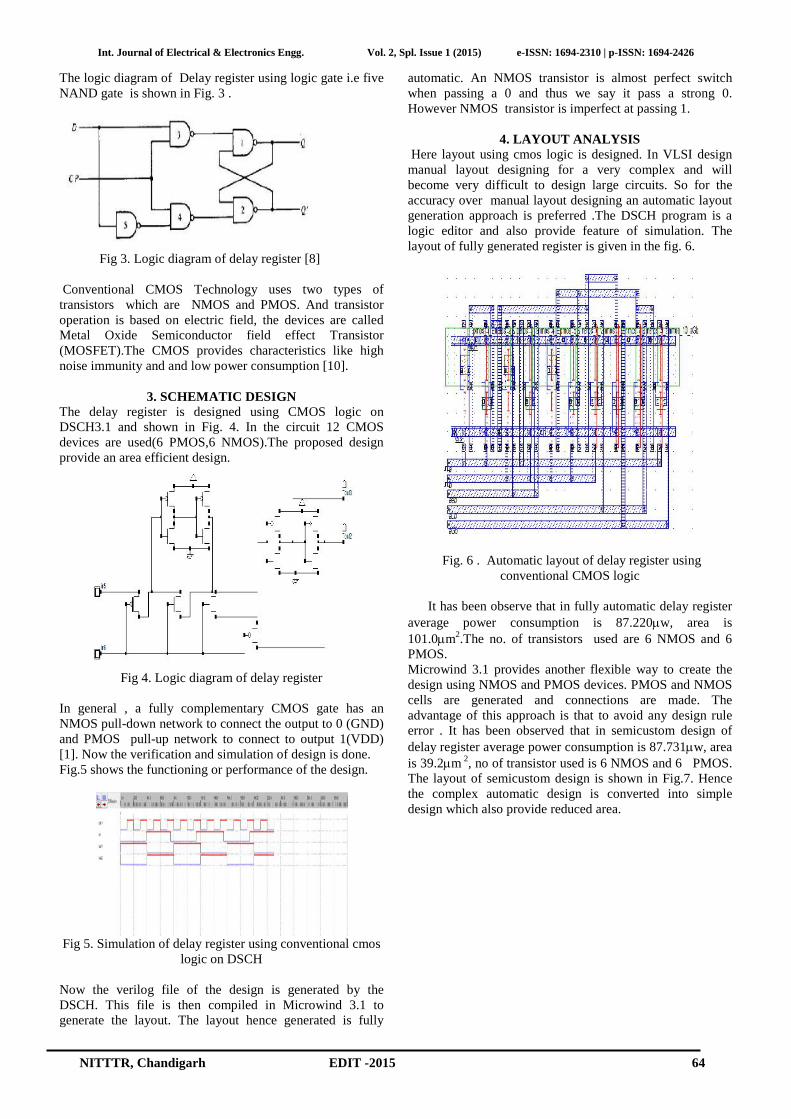
The logic diagram of Delay register using logic gate i.e fiveNAND gate is shown in Fig. 3 .
Fig 3. Logic diagram of delay register [8]
Conventional CMOS Technology uses two types oftransistors which are NMOS and PMOS. And transistoroperation is based on electric field, the devices are calledMetal Oxide Semiconductor field effect Transistor(MOSFET).The CMOS provides characteristics like highnoise immunity and and low power consumption [10].
3. SCHEMATIC DESIGNThe delay register is designed using CMOS logic onDSCH3.1 and shown in Fig. 4. In the circuit 12 CMOSdevices are used(6 PMOS,6 NMOS).The proposed designprovide an area efficient design.
Fig 4. Logic diagram of delay register
In general , a fully complementary CMOS gate has anNMOS pull-down network to connect the output to 0 (GND)and PMOS pull-up network to connect to output 1(VDD)[1]. Now the verification and simulation of design is done.Fig.5 shows the functioning or performance of the design.
Fig 5. Simulation of delay register using conventional cmoslogic on DSCH
Now the verilog file of the design is generated by theDSCH. This file is then compiled in Microwind 3.1 togenerate the layout. The layout hence generated is fully
automatic. An NMOS transistor is almost perfect switchwhen passing a 0 and thus we say it pass a strong 0.However NMOS transistor is imperfect at passing 1.
4. LAYOUT ANALYSISHere layout using cmos logic is designed. In VLSI design
manual layout designing for a very complex and willbecome very difficult to design large circuits. So for theaccuracy over manual layout designing an automatic layoutgeneration approach is preferred .The DSCH program is alogic editor and also provide feature of simulation. Thelayout of fully generated register is given in the fig. 6.
Fig. 6 . Automatic layout of delay register usingconventional CMOS logic
It has been observe that in fully automatic delay registeraverage power consumption is 87.220w, area is101.0m2.The no. of transistors used are 6 NMOS and 6PMOS.Microwind 3.1 provides another flexible way to create thedesign using NMOS and PMOS devices. PMOS and NMOScells are generated and connections are made. Theadvantage of this approach is that to avoid any design ruleerror . It has been observed that in semicustom design ofdelay register average power consumption is 87.731w, areais 39.2m 2, no of transistor used is 6 NMOS and 6 PMOS.The layout of semicustom design is shown in Fig.7. Hencethe complex automatic design is converted into simpledesign which also provide reduced area.
Int. Journal of Electrical & Electronics Engg. Vol. 2, Spl. Issue 1 (2015) e-ISSN: 1694-2310 | p-ISSN: 1694-2426
65 NITTTR, Chandigarh EDIT-2015
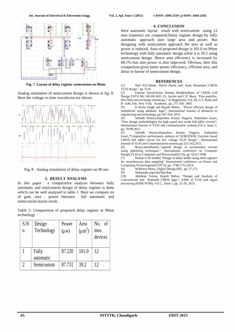
Fig. 7. Layout of delay register semicustom on 90nm
Analog simulation of semicustom design is shown in fig. 8.Here the voltage vs time waveforms are shown.
Fig. 8 . Analog simulation of delay register on 90 nm
5. RESULT ANALYSISIn this paper a comparative analysis between fullyautomatic and semicustom design of delay register is donewhich can be well analysed in table 1. Here we compare noof gate, area , power between full automatic andsemicustom layout result.
Table 2: Comparision of proposed delay register at 90nmtechnology
S.No
DesignTechnology
Power(w)
Area(m2)
No. ofmosdevices
1 Fullyautomatic
87.220 101.0 12
2 Semicustom 87.731 39.2 12
6 .CONCLUSIONHere automatic layout result with semicustom using 12mos transistor are compared.Delay register design by fullyautomatic approach uses large area and power. Butdesigning with semicustom approach the area as well aspower is reduced. Area of proposed design is 101.0 on 90nmtechnology with fully automatic design while it is 39.2 usingsemicustom design. Hence area efficiency is increased by68.1%.Ans also power is also improved. Obvious, here thiscomparison gives batter power efficiency, efficient area, anddelay in favour of semicustom design.
REFERENCES[1] Neil H.E.Weste, David Harris and Ayan Banaerjee,”CMOSVLSI design ” pp. 9-10.[2] Eitenne Sicard,Sonia Delmas Bendhia,Basic of CMOS CellDesign,TATA Mc GRAW-Hill. I.S. Jacobs and C.P. Bean, “Fine particles,thin films and exchange anisotropy,” in Magnetism, Vol. III, G.T. Rado andH. Suhl, Eds. New York, Academic, pp. 271-350, 1963.[3] K Richa Singh and Rajesh Mehra , “Power efficient design ofmultiplexer using adiabatic logic”, International Journal of advances inengineering and technology, pp 247-254, 2013.[4] Subodh Wairya,Rajendera Kumar Nagaria, Sudarshan tiwari,“New design methodologies for high speed mix mode full adder circuits”,International Journal of VLSI and communication systems,Vol 2, Issue 2,pp. 78-98,2011.[5] Subodh Wairya,Rajendera Kumar Nagaria, Sudarshantiwari,”Comparitive performance analysis of XOR/XNOR Function basedCMOS full adder circuit for low voltage VLSI design’’, InternationalJournal of VLSI and Communication systems,pp 221-242,2012.[6] Boyer,aboulhamid,’’optimal design of synchronous circuitsusing pipelining techniques’’, International conference on ComputerDesign:VLSI in Computers and Processors(ICCD), pp. 62-67,1998.[7] Kumar,V.M Senthil,”Design of delay buffer using shift registersfor asynchronous data sampling” International conference on Power andComputing Technologies(ICCPCT), pp. 1748-1752,2014.[8] M.Morris Mano, Digital Design,PHI, pp. 57,171.[9] Wikipedia.org/wiki/flip-flop.[10] Akhilesh Verma, Rajesh Mehra, “Design and Analysis ofConventional and Rationed CMOS logic”, IOSR of VLSI and signalprocessing (IOSR-JVSR), Vol 2 , Issue 2, pp. 25-29, 2013.