Embed Size (px)
Citation preview
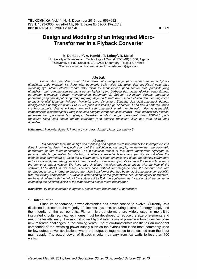
TELKOMNIKA, Vol.11, No.4, December 2013, pp. 669~682 ISSN: 1693-6930, accredited A by DIKTI, Decree No: 58/DIKTI/Kep/2013 DOI: 10.12928/TELKOMNIKA.v11i4.1785 669
Received May 30, 2013; Revised September 30, 2013; Accepted October 22, 2013
Design and Modeling of an Integrated Micro-Transformer in a Flyback Converter
M. Derkaoui*1, A. Hamid1, T. Lebey2, R. Melati1 1 University of Sciences and Technology of Oran (USTO-MB) 31000, Algeria
2University of Paul Sabatier, LAPLACE Laboratory, Toulouse, France *Corresponding author, e-mail: [email protected]
Abstrak Desain dan pemodelan suatu trafo mikro untuk integrasinya pada sebuah konverter flyback
dihadirkan pada makalah ini. Parameter geometris trafo mikro ditentukan dari spesifikasi catu daya switching-nya. Model elektris π-dari trafo mikro ini menekankan pada semua efek parasitik yang dihasilkam oleh penumpukan berbagai bahan lapisan yang berbeda dan memungkinkan penghitungan parameter teknologis dengan menggunakan parameter S. Sebuah penentuan dimensi parameter geometris yang baik dapat mengurangi rugi-rugi daya pada trafo mikro secara efisien dan memungkinkan tercapainya nilai tegangan keluaran konverter yang diinginkan. Simulasi efek elektromagnetik dengan menggunakan perangkat lunak FEMLAB3.1 pada dua kasus juga dihadirkan. Pada kasus pertama, tanpa inti ferromagnetik, dan yang kedua dengan inti ferromagnetik untuk memilih trafo mikro yang memiliki kompatibilitas elektromagnetik yang lebih baik dengan komponen di sekitarnya. Untuk menvalidasi dimensi geometris dan parameter teknogianya, dilakukan simulasi dengan perangkat lunak PSIM6.0 pada rangkaian listrik yang setara dengan konverter yang memiliki rangkaian listrik dari trafo mikro yang dihasilkan. Kata kunci: konverter fly-back, integrasi, micro-transformer planar, parameter S
Abstract This paper presents the design and modeling of a square micro-transformer for its integration in a
flyback converter. From the specifications of the switching power supply, we determined the geometric parameters of this micro-transformer. The π-electrical model of this micro-transformer highlights all parasitic effects generated by stacking of different material layers and permits to calculate the technological parameters by using the S-parameters. A good dimensioning of the geometrical parameters reduces efficiently the energy losses in the micro-transformer and permits to reach the desirable value of the converter output voltage. We have also simulated the electromagnetic effects with the help of the software FEMLAB3.1 in two cases. The first case, without ferromagnetic core, the second case with ferromagnetic core, in order to choose the micro-transformer that has better electromagnetic compatibility with the vicinity components. To validate dimensioning of the geometrical and technological parameters, we have simulated with the help of the software PSIM6.0, the equivalent electrical circuit of the converter containing the electrical circuit of the dimensioned planar micro-transformer. Keywords: fly-back converter, integration, planar micro-transformer, S-parameters 1. Introduction
Since its appearance, power electronics has never ceased to evolve. Currently, this discipline is present in the majority of electrical systems, ensuring control of energy supply and the integrity of the components. Planar micro-transformers are widely used in monolithic integrated circuits; so, new techniques must be developed to reduce the size of elements and reach better efficiency. The monolithic and hybrid integration of power electronic devices pose new research challenges in the coming years. The micro-transformer constitutes an important component of the switching power supply such as the flyback that is the most commonly used for low output power applications where the output voltage needs to be isolated from the input main supply. The output power of flyback circuits may vary from few watts to less than 100 watts.
ISSN: 1693-6930
TELKOMNIKA Vol. 11, No. 4, December 2013: 669 – 682
670
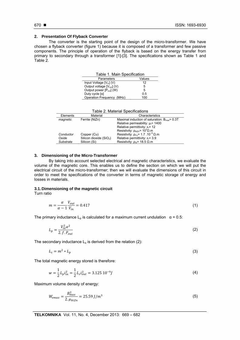
2. Presentation Of Flyback Converter The converter is the starting point of the design of the micro-transformer. We have
chosen a flyback converter (figure 1) because it is composed of a transformer and few passive components. The principle of operation of the flyback is based on the energy transfer from primary to secondary through a transformer [1]-[3]. The specifications shown as Table 1 and Table 2.
Table 1. Main Specification Parameters Values
Input Voltage [Vin] (V) 12 Output voltage [Vout] (V) 5 Output power [Pout] (W) 5 Duty cycle [α] 0.5 Operation Frequency (MHz) 100
Table 2. Material Specifications Elements Material Characteristics
magnetic Ferrite (NiZn) Maximal induction of saturation: Bmax= 0.3T Relative permeability: μr= 1400 Relative permittivity: εr= 12 Resistivity: ρNiZn= 103Ω.m
Conductor Copper (Cu) Resistivity: ρCu= 1.7 .10−8 Ω.m Oxide Silicon dioxide (SiO2) Relative permittivity: εr= 3.9 Substrate Silicon (Si) Resistivity: ρSi= 18.5 Ω.m
3. Dimensioning of the Micro-Transformer
By taking into account selected electrical and magnetic characteristics, we evaluate the volume of the magnetic core. This enables us to define the section on which we will put the electrical circuit of the micro-transformer; then we will evaluate the dimensions of this circuit in order to meet the specifications of the converter in terms of magnetic storage of energy and losses in materials.
3.1. Dimensioning of the magnetic circuit Turn ratio
10.417
(1)
The primary inductance Lp is calculated for a maximum current undulation α = 0.5:
2. . (2)
The secondary inductance Ls is derived from the relation (2):
∗ (3) The total magnetic energy stored is therefore:
12
12
3.125 10 (4)
Maximum volume density of energy:
2.25.59 /
(5)
TELKOMNIKA ISSN: 1693-6930
Design and Modeling of an Integrated Micro-Transformer in a Flyback Converter (Derkaoui)
671
Volume of the core:
1.2210
(6)
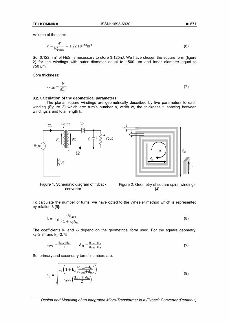
So, 0.122mm3 of NiZn is necessary to store 3.125nJ. We have chosen the square form (figure 2) for the windings with outer diameter equal to 1500 µm and inner diameter equal to 750 µm. Core thickness:
e
(7)
3.2. Calculation of the geometrical parameters
The planar square windings are geometrically described by five parameters to each winding (Figure 2) which are: turn’s number n, width w, the thickness t, spacing between windings s and total length lt.
Figure 1. Schematic diagram of flyback converter
Figure 2. Geometry of square spiral windings
[4]
To calculate the number of turns, we have opted to the Wheeler method which is represented by relation 8 [5]:
L k µn d
1 k A (8)
The coefficients k1 and k2 depend on the geometrical form used. For the square geometry: k1=2,34 and k2=2,75.
d ,
A (x)
So, primary and secondary turns’ numbers are:
nL 1 k
d dd d
k µd d
2
(9)

ISSN: 1693-6930
TELKOMNIKA Vol. 11, No. 4, December 2013: 669 – 682
672
n m. n (10) The calculation of these two parameters (Primary thickness and width) depends on skin thickness (equation 11) which determines the width of the zone where the current concentrates in a conductor [6] [7] [8].
δρ
π.μ . f (11)
To circumvent the problem of the skin effect and make the current flowing in the entire conductor, it is necessary to fulfill one of the following conditions:
2 2 (11)
The current density for x ranging from 0 to t/2 is given by;
j x j e δ e δ (12) The average value of the current density is:
j je δ 1
2 (13)
One of the two values t or w set in order to find the other. The width of the primary conductor wp is is derived from the equations (14) and (15) for a value of t = 2.δ (t: thickness of the conductors of primary and secondary).
i Sc . j (14)
Sc w . t (15) Where Scp: primary conductor’s section. In most cases, micro-conductors are in contact with the substrate that has good conduction properties of temperature. This allows us to use the boundaries conditions: j 10 A/m² [9]. Primary spacing
sd d 2.w . n
2. n 1 (16)
Primary total length
lt 4n d n 1 s n .w s (17)
We have taken the same spacing for both the primary and secondary windings:
wd d 2. s . n 1
2. n (18)
Secondary total length:
l 4. n . d n 1 . s n .w s (19)
TELKOMNIKA ISSN: 1693-6930
Design and Modeling of an Integrated Micro-Transformer in a Flyback Converter (Derkaoui)
673
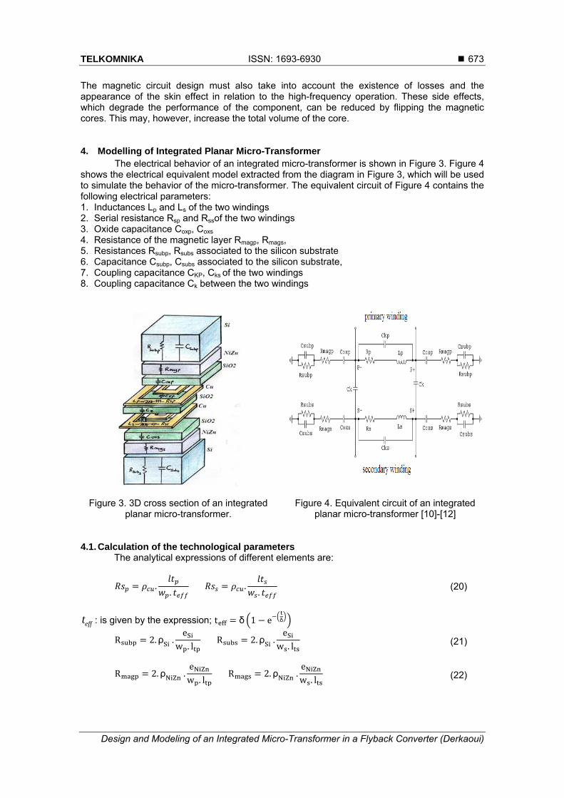
The magnetic circuit design must also take into account the existence of losses and the appearance of the skin effect in relation to the high-frequency operation. These side effects, which degrade the performance of the component, can be reduced by flipping the magnetic cores. This may, however, increase the total volume of the core. 4. Modelling of Integrated Planar Micro-Transformer
The electrical behavior of an integrated micro-transformer is shown in Figure 3. Figure 4 shows the electrical equivalent model extracted from the diagram in Figure 3, which will be used to simulate the behavior of the micro-transformer. The equivalent circuit of Figure 4 contains the following electrical parameters: 1. Inductances Lp and Ls of the two windings 2. Serial resistance Rsp and Rssof the two windings 3. Oxide capacitance Coxp, Coxs 4. Resistance of the magnetic layer Rmagp, Rmags, 5. Resistances Rsubp, Rsubs associated to the silicon substrate 6. Capacitance Csubp, Csubs associated to the silicon substrate, 7. Coupling capacitance CKP, Cks of the two windings 8. Coupling capacitance Ck between the two windings
Figure 3. 3D cross section of an integrated planar micro-transformer.
Figure 4. Equivalent circuit of an integrated planar micro-transformer [10]-[12]
4.1. Calculation of the technological parameters
The analytical expressions of different elements are:
..
.. (20)
efft : is given by the expression; t δ 1 e δ
R 2.ρ .e
w . lR 2.ρ .
ew . l (21)
R 2.ρ .ew . l
R 2.ρ .ew . l (22)
ISSN: 1693-6930
TELKOMNIKA Vol. 11, No. 4, December 2013: 669 – 682
674
C12. ε .
w . lt
C12. ε .
w . lt
(23)
C12. ε .
w . le
C12. ε .
w . le
(24)
C12. ε .
t. ls
C12. ε .
t. ls (25)
C ε .dt
(26)
4.2. Concept of S-parameters
The scattering parameters of the micro-transformer can be easily obtained from the localized model. The S-parameters of Figure 4 are calculated as follows [13]: First, we calculate the ABCD matrices for each block.
1 01
11
1
10 1
.
1
10 1
1 01
11
1
11
0 1
(x)
Where . . Next, we can combine the blocks α, β, γ, δ, ε, φ in cascade:
. . . . . (x)
Then, we can combine the large intermediate block I with block φ in parallel. The final ABCD matrix of the entire transformer F is given below:
1.
.
. . (x)
Finally, we can convert the A, B, C, D parameters to S-parameters as follows:
TELKOMNIKA ISSN: 1693-6930
Design and Modeling of an Integrated Micro-Transformer in a Flyback Converter (Derkaoui)
675
SA
BZ C . Z D
ABZ C . Z D
S2. A . D B . C
ABZ C . Z D
(27)
S2
ABZ C . Z D
SA
BZ C . Z D
ABZ C . Z D
(28)
Here, Z0 is the characteristic impedance of the line. Also, note that due to reciprocity, we will have A . D B . C 1; therefore, S12=S21. 5. Geometrical And Electrical Parameters Results 5.1. Geometric dimensioning results
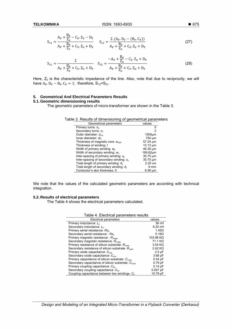
The geometric parameters of micro-transformer are shown in the Table 3.
Table 3. Results of dimensioning of geometrical parameters Geometrical parameters values
Primary turns: np 5 Secondary turns: ns 2 Outer diameter: dout 1500µm Inner diameter: din 750 µm Thickness of magnetic core: eNiZn 57.24 µm Thickness of winding: t 13.13 µm Width of primary winding: wp 46.39 µm Width of secondary winding: ws 169.62µm Inter-spacing of primary winding: sp 35.75 µm Inter-spacing of secondary winding: ss 35.75 µm Total length of primary winding: ltp 2.25 cm Total length of secondary winding: lts
Conductor’s skin thickness: δ 9 mm
6.56 µm
We note that the values of the calculated geometric parameters are according with technical integration. 5.2. Results of electrical parameters
The Table 4 shows the electrical parameters calculated.
Table 4. Electrical parameters results Electrical parameters values
Primary inductance: Lp
Secondary inductance: Ls Primary serial resistance: Rsp
Secondary serial resistance : Rss Primary magnetic resistance : Rmagp Secondary magnetic resistance :Rmags
Primary resistance of silicon substrate :Rsubp
Secondary resistance of silicon substrate :Rsubs
Primary oxide capacitance :Coxp
Secondary oxide capacitance :Coxs
Primary capacitance of silicon substrate :Csubp
Secondary capacitance of silicon substrate :Csubs
Primary coupling capacitance :Ckp
Secondary coupling capacitance :Cks
Coupling capacitance between two windings :Ck
36 nH 6.25 nH
1.45Ω 0.16Ω
103.98 KΩ 71.1 KΩ 3.54 KΩ 2.42 KΩ
2.5 pF 3.66 pF 0.54 pF 0.79 pF 0.14 pF
0.057 pF 10.79 pF
ISSN: 1693-6930
TELKOMNIKA Vol. 11, No. 4, December 2013: 669 – 682
676
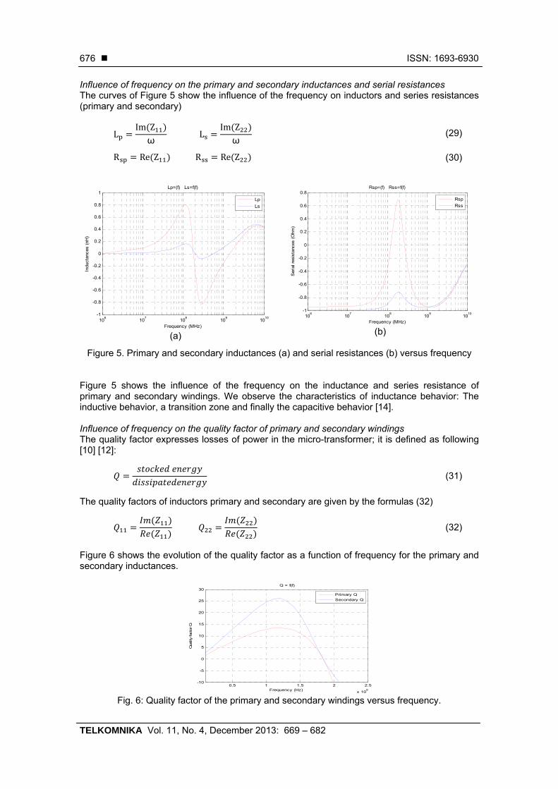
Influence of frequency on the primary and secondary inductances and serial resistances The curves of Figure 5 show the influence of the frequency on inductors and series resistances (primary and secondary)
LIm Z
ωL
Im Zω
(29)
R Re Z R Re Z (30)
(a)
(b)
Figure 5. Primary and secondary inductances (a) and serial resistances (b) versus frequency
Figure 5 shows the influence of the frequency on the inductance and series resistance of primary and secondary windings. We observe the characteristics of inductance behavior: The inductive behavior, a transition zone and finally the capacitive behavior [14]. Influence of frequency on the quality factor of primary and secondary windings The quality factor expresses losses of power in the micro-transformer; it is defined as following [10] [12]:
(31)
The quality factors of inductors primary and secondary are given by the formulas (32)
(32)
Figure 6 shows the evolution of the quality factor as a function of frequency for the primary and secondary inductances.
Fig. 6: Quality factor of the primary and secondary windings versus frequency.
106
107
108
109
1010
-1
-0.8
-0.6
-0.4
-0.2
0
0.2
0.4
0.6
0.8
1Lp=(f) Ls=f(f)
Frequency (MHz)
Indu
ctan
ces
(nH
)
Lp
Ls
106
107
108
109
1010
-1
-0.8
-0.6
-0.4
-0.2
0
0.2
0.4
0.6
0.8Rsp=(f) Rss=f(f)
Frequency (MHz)
Ser
ial r
esis
tanc
es (
Ohm
)
Rsp
Rss
0.5 1 1.5 2 2.5
x 108
-10
-5
0
5
10
15
20
25
30 Q = f(f)
Frequency (Hz)
Qua
lity
fact
or Q
Primary Q
Secondary Q
TELKOMNIKA ISSN: 1693-6930
Design and Modeling of an Integrated Micro-Transformer in a Flyback Converter (Derkaoui)
677
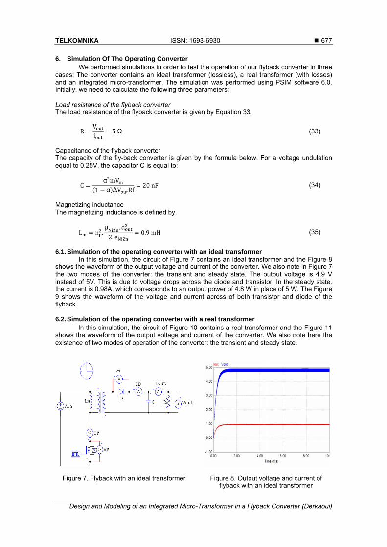
6. Simulation Of The Operating Converter We performed simulations in order to test the operation of our flyback converter in three
cases: The converter contains an ideal transformer (lossless), a real transformer (with losses) and an integrated micro-transformer. The simulation was performed using PSIM software 6.0. Initially, we need to calculate the following three parameters:
Load resistance of the flyback converter The load resistance of the flyback converter is given by Equation 33.
RVi
5 Ω
(33)
Capacitance of the flyback converter The capacity of the fly-back converter is given by the formula below. For a voltage undulation equal to 0.25V, the capacitor C is equal to:
Cα mV
1 α ∆V Rf20nF
(34)
Magnetizing inductance The magnetizing inductance is defined by,
L n .µ . d
2. e0.9mH
(35)
6.1. Simulation of the operating converter with an ideal transformer
In this simulation, the circuit of Figure 7 contains an ideal transformer and the Figure 8 shows the waveform of the output voltage and current of the converter. We also note in Figure 7 the two modes of the converter: the transient and steady state. The output voltage is 4.9 V instead of 5V. This is due to voltage drops across the diode and transistor. In the steady state, the current is 0.98A, which corresponds to an output power of 4.8 W in place of 5 W. The Figure 9 shows the waveform of the voltage and current across of both transistor and diode of the flyback.
6.2. Simulation of the operating converter with a real transformer
In this simulation, the circuit of Figure 10 contains a real transformer and the Figure 11 shows the waveform of the output voltage and current of the converter. We also note here the existence of two modes of operation of the converter: the transient and steady state.
Figure 7. Flyback with an ideal transformer
Figure 8. Output voltage and current of flyback with an ideal transformer
ISSN: 1693-6930
TELKOMNIKA Vol. 11, No. 4, December 2013: 669 – 682
678
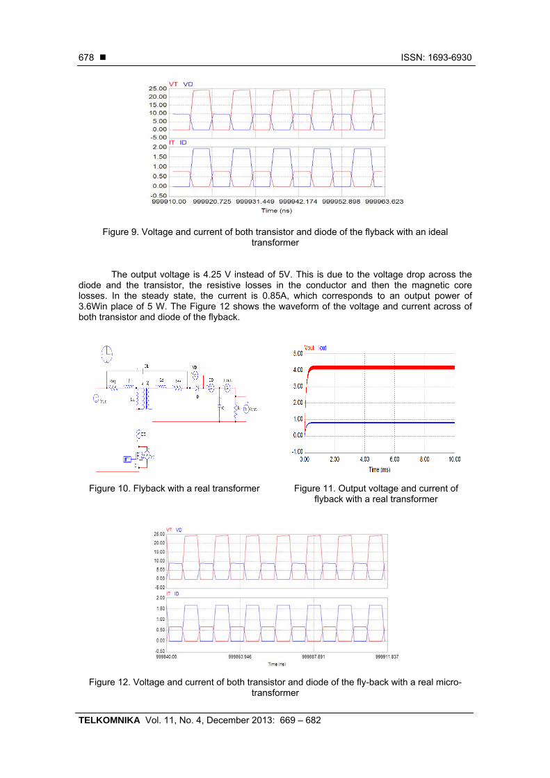
Figure 9. Voltage and current of both transistor and diode of the flyback with an ideal transformer
The output voltage is 4.25 V instead of 5V. This is due to the voltage drop across the diode and the transistor, the resistive losses in the conductor and then the magnetic core losses. In the steady state, the current is 0.85A, which corresponds to an output power of 3.6Win place of 5 W. The Figure 12 shows the waveform of the voltage and current across of both transistor and diode of the flyback.
Figure 10. Flyback with a real transformer
Figure 11. Output voltage and current of flyback with a real transformer
Figure 12. Voltage and current of both transistor and diode of the fly-back with a real micro-transformer
TELKOMNIKA ISSN: 1693-6930
Design and Modeling of an Integrated Micro-Transformer in a Flyback Converter (Derkaoui)
679
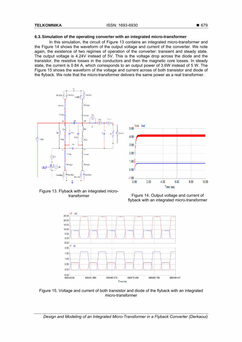
6.3. Simulation of the operating converter with an integrated micro-transformer In this simulation, the circuit of Figure 13 contains an integrated micro-transformer and the Figure 14 shows the waveform of the output voltage and current of the converter. We note again, the existence of two regimes of operation of the converter: transient and steady state. The output voltage is 4.24V instead of 5V. This is the voltage drop across the diode and the transistor, the resistive losses in the conductors and then the magnetic core losses. In steady state, the current is 0.84 A, which corresponds to an output power of 3.6W instead of 5 W. The Figure 15 shows the waveform of the voltage and current across of both transistor and diode of the flyback. We note that the micro-transformer delivers the same power as a real transformer.
Figure 13. Flyback with an integrated micro-
transformer
Figure 14. Output voltage and current of
flyback with an integrated micro-transformer
Figure 15. Voltage and current of both transistor and diode of the flyback with an integrated micro-transformer
ISSN: 1693-6930
TELKOMNIKA Vol. 11, No. 4, December 2013: 669 – 682
680
7. The Flyback Converter Efficiency The efficiency of converter (Formula 36) tells us about his performance. Pj is copper
losses and Pf is Iron losses.
ηP P P
p (36)
. (37)
. (38)
(39)
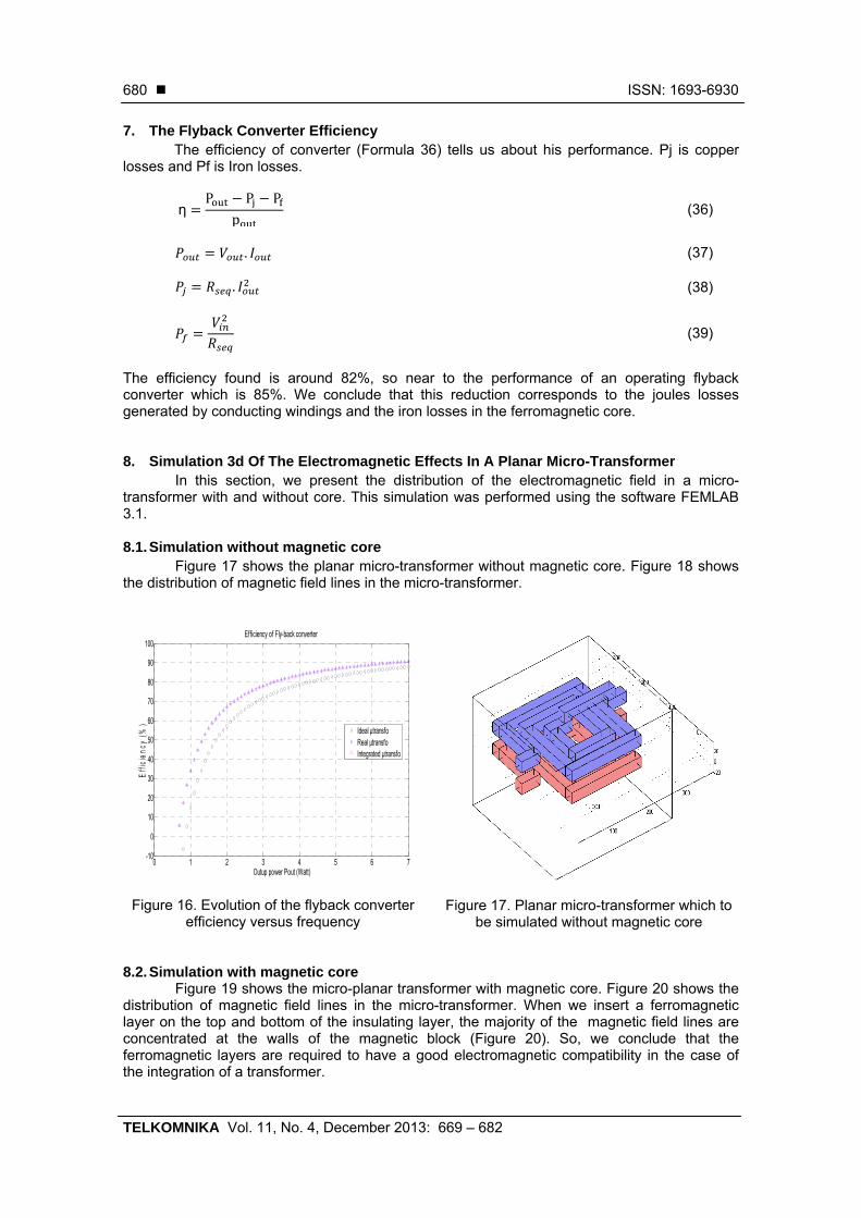
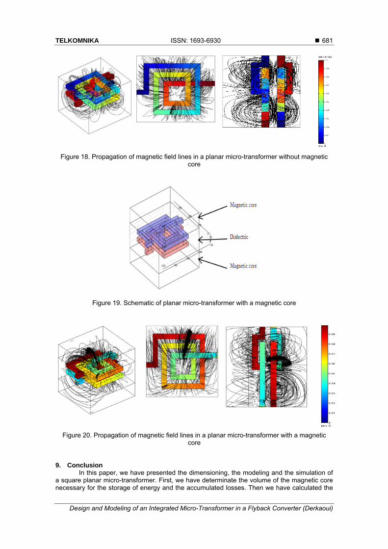
The efficiency found is around 82%, so near to the performance of an operating flyback converter which is 85%. We conclude that this reduction corresponds to the joules losses generated by conducting windings and the iron losses in the ferromagnetic core. 8. Simulation 3d Of The Electromagnetic Effects In A Planar Micro-Transformer In this section, we present the distribution of the electromagnetic field in a micro-transformer with and without core. This simulation was performed using the software FEMLAB 3.1. 8.1. Simulation without magnetic core Figure 17 shows the planar micro-transformer without magnetic core. Figure 18 shows the distribution of magnetic field lines in the micro-transformer.
Figure 16. Evolution of the flyback converter efficiency versus frequency
Figure 17. Planar micro-transformer which to
be simulated without magnetic core 8.2. Simulation with magnetic core Figure 19 shows the micro-planar transformer with magnetic core. Figure 20 shows the distribution of magnetic field lines in the micro-transformer. When we insert a ferromagnetic layer on the top and bottom of the insulating layer, the majority of the magnetic field lines are concentrated at the walls of the magnetic block (Figure 20). So, we conclude that the ferromagnetic layers are required to have a good electromagnetic compatibility in the case of the integration of a transformer.
0 1 2 3 4 5 6 7-10
0
10
20
30
40
50
60
70
80
90
100Efficiency of Fly-back converter
Outup power Pout (Watt)
Effi
cien
cy (
%)
Ideal µtransfoReal µtransfoIntegrated µtransfo
TELKOMNIKA ISSN: 1693-6930
Design and Modeling of an Integrated Micro-Transformer in a Flyback Converter (Derkaoui)
681
Figure 18. Propagation of magnetic field lines in a planar micro-transformer without magnetic core
Figure 19. Schematic of planar micro-transformer with a magnetic core
Figure 20. Propagation of magnetic field lines in a planar micro-transformer with a magnetic core
9. Conclusion
In this paper, we have presented the dimensioning, the modeling and the simulation of a square planar micro-transformer. First, we have determinate the volume of the magnetic core necessary for the storage of energy and the accumulated losses. Then we have calculated the
ISSN: 1693-6930
TELKOMNIKA Vol. 11, No. 4, December 2013: 669 – 682
682
geometrical parameters taking into account the maximum area occupied by the windings. We have used the S-parameters method to determine the technological parameters.
Next, by using a software simulation PSIM6.0, we have compared the waveforms of the converter output voltages for the three simulations. Finally, by using the software FEMLAB3.1, we have visualized the electromagnetic phenomenon in planar micro-transformers, with and without magnetic core. The aim of this simulation is to study the electromagnetic compatibility of the micro-transformer with the vicinity components in the converter. We conclude that the results of dimensioning in this paper are interesting indeed. References [1] V Boyer, N Godefroy. Alimentation à découpage Flyback. M1-IUP GEII. Université Joseph Fourier. [2] Q Laurent, Y Heinrich. Réalisation d'un convertisseur Flyback. Projet ENPU, INSA. Strasbourg. [3] JYs Le Chenadec. Alimentation à découpage, Etude, Choix et Dimensionnement des Alimentations à
Découpage Usuelles. Lycée Louis ARMAND. Strasbourg. [4] P Gomes. Monolithic Power Combiners in CMOS technologies for WLAN applications. Instituto
Superior Técnico. Universida de Técnica de Lisboa. 2011. [5] B Estibals, C Alonso, A Salles, J Schanen, R Perret. “Validation d’outils de simulation d’éléments
inductifs pour convertisseur statique intégré“. Laboratoire d’Analyse et d’Architecture des Systèmes LAAS du CNRS. Toulouse et Laboratoire d’Electrotechnique de Grenoble. France.
[6] Fu Keung Wong. High Frequency Transformer for Switching Mode Power Supplies. School of Microelectronic Engineering. Faculty of Engineering and Information Technology Griffith University. Brisbane. Australia. 2004.
[7] A Ghannam. Conception et intégration "above IC" d’inductances à fort coefficient de surtension pour applications de puissance RF. Université Toulouse III– Paul Sabatier. 2010.
[8] X Margueron. Elaboration sans prototypage du circuit équivalent de transformateurs de type planar. Laboratoire d'Electrotechnique de Grenoble. Université Joseph Fourier. 2006.
[9] C Alonso. “Contribution à l’optimisation, la gestion et le traitement de l’énergie“. Université Paul Sabatier – Toulouse III. 2003.
[10] D Kehrer. “Design of Monolithic Integrated Lumped Transformers in Silicon-based Technologie sup to 20 GHz”. Wien University. 2000.
[11] R Thüringer. “Characterization of Integrated Lumped Inductors and Transformers”. Wien University. 2002.
[12] Y Maycvskiy. Analysis and Modeling of Monolithic On-Chip Transformers on Silicon Substrates. Oregon State University. United States of America. 2005.
[13] Shwetabh Verma, Jose M Cruz. “On-chip Inductors and Transformers”. SMLI TR-99-79. 1999. [14] YK Koutsoyannopoulos. Systematic Analysis and Modeling of Integrated Inductors and Transformers
in RF IC Design. Analog and Digital Signal Processing. 2000; 47(8): 699. [15] Xun Liu, S Y Ron Hui. Equivalent Circuit Modeling of a Multilayer Planar Winding Array Structure for
Use in a Universal Contactless Battery Charging Platform. IEEE transactions on power electronics. 2007; 22(1).
[16] A Salles. Conception d’éléments passifs magnétiques pour convertisseurs de faible puissance. Université Toulouse III. Paul Sabatier. 2008.
[17] S Musunuri, PL Chapman, J Zou, C Liu. Design Issues for Monolithic DC–DC Converters. IEEE Transactions On Power Electronics. 2005; 20(3).
[18] Kharagpur. DC to DC Converters, Fly-Back Type Switched Mode Power Supply. Version 2 EE IIT. [19] Andreas Weisshaar. Analysis and Modeling of Monolithic On-Chip Transformers on Silicon. 2005. [20] Xu Daoxian. Characterization and modeling of Micro-wave spiral Transformers and inductors. Peking
University. China. 2005. [21] O'Donnell, Magali Brunet, Paul McCloskey, Joe O’Brien, Seán Cian, Ó Mathúna. Micro transformers
and Inductors using Permalloy Thin Films. Cork. Ireland. [22] B Allard, S Azzopardi, Jc crebier, Z Khatir, E Labouré, T Lebey, Jl sanchez.Enjeux Et Défis de
L'intégration 3D en Électronique de Puissance. ISP3D. [23] Alberto M Pernía, Miguel J Prieto, Juan M Lopera. High Power Density DC/DC Converter Using Thick-
Film Hybrid Technology . Universidad de Oviedo. Campus de Viesques. Gijón (Asturias). Spain. [24] K Ammous. Contribution à la construction systématique des modèles moyens de convertisseur de
puissance. Institut national des sciences appliquées. Lyon. 2002.