Embed Size (px)
Citation preview
Design for Manufacturability of Rigid Multi-Layer Boards
By: Tom Hausherr
DFM Guidelines INTRODUCTION
ii of 91
CONTENTS SECTION PAGE 1 INTRODUCTION......................................................................................................1-3 2 RAW MATERIALS SELECTION..............................................................................2-3
2.1 Material Selection and Panel Utilization ............................................................................................2-3 2.2 Material Properties ..............................................................................................................................2-3 2.3 FR-4 Base Material and Thickness.....................................................................................................2-3 2.4 FR-4 Prepreg Designation and Thickness ..........................................................................................2-3 2.5 Copper Clad for Materials...................................................................................................................2-3 2.6 Resistivity of Copper...........................................................................................................................2-3 2.7 Current Carrying Capacity of Copper.................................................................................................2-3 2.8 Panel Sizes and Usable Area...............................................................................................................2-3 2.9 Multi-layer Usable Area Diagrams.....................................................................................................2-3 2.10 Multi-layer Lay-up Recommendation ................................................................................................2-3 2.11 Recommended Lay-up for 2 – 12 Layer Boards ................................................................................2-3 2.12 Recommended Lay-up for 14 & 16 Layer Boards .............................................................................2-3 2.13 Buried CapacitanceTM..........................................................................................................................2-3 2.14 Multi-layer Lay-up ..............................................................................................................................2-3 2.15 Fabrication Drawing............................................................................................................................2-3
3 COMPLEXITY FACTOR CLASSIFICATION ...........................................................3-3 3.1 Objective..............................................................................................................................................3-3 3.2 Complexity Factors Matrix .................................................................................................................3-3 3.3 Constraints ...........................................................................................................................................3-3 3.4 Etch Factor...........................................................................................................................................3-3 3.5 Plated Finished Hole Tolerance ..........................................................................................................3-3 3.6 Unplated Drilled Slot Size Tolerance .................................................................................................3-3 3.7 Minimum and Maximum Drill Diameter ...........................................................................................3-3 3.8 Drill Selection......................................................................................................................................3-3 3.9 Annular Ring .......................................................................................................................................3-3 3.10 Tear Drop Pads ....................................................................................................................................3-3 3.11 Clearance Pad ......................................................................................................................................3-3 3.12 Tenting of Unplated Holes ..................................................................................................................3-3 3.13 Finished Board Thickness ...................................................................................................................3-3 3.14 Aspect Ratio Plating Capability..........................................................................................................3-3 3.15 Overall Finished Profile Tolerance.....................................................................................................3-3 3.16 Tab Routing .........................................................................................................................................3-3 3.17 Scored Board Profiling........................................................................................................................3-3 3.18 Hand Finishing Operations .................................................................................................................3-3 3.19 Edge Bevel...........................................................................................................................................3-3
4 PLATING OPTIONS.................................................................................................4-3 4.1 Gold Plating.........................................................................................................................................4-3 4.2 Selective or Double Image Plating .....................................................................................................4-3 4.3 Edge Connector Plating.......................................................................................................................4-3
5 SOLDER MASK........................................................................................................5-3 5.1 Objective..............................................................................................................................................5-3 5.2 Tenting of Via Holes with Solder Mask .............................................................................................5-3 5.3 Peelable Solder Mask ..........................................................................................................................5-3

DFM Guidelines INTRODUCTION
iii of 91
6 BLIND AND BURIED VIA (BBV) BOARDS..............................................................6-3 6.1 General description..............................................................................................................................6-3
7 CONTROLLED IMPEDANCE ..................................................................................7-3 7.1 Characteristic Impedance ....................................................................................................................7-3 7.2 Impedance Structures ..........................................................................................................................7-3
8 Testing ......................................................................................................................8-3 8.1 Testing .................................................................................................................................................8-3 8.2 Beep Test Coupon ...............................................................................................................................8-3
9 MOUNTING HARDWARE & GEOMETRIES...........................................................9-3 9.1 Metric Nut, Screw and Washer Hardware Chart................................................................................9-3 9.2 Metric Plated Through Mounting Holes.............................................................................................9-3 9.3 Metric Non-Plated Through Mounting Holes ....................................................................................9-3 9.4 English Nut, Screw and Washer Hardware Chart ..............................................................................9-3 9.5 English Plated Through Mounting Holes ...........................................................................................9-3 9.6 English Non-Plated Through Mounting Holes...................................................................................9-3
10 THROUGH-HOLE PADSTACKS ...........................................................................10-3 10.1 Plated Through-holes ........................................................................................................................10-3 10.2 Non-Plated Through-holes ................................................................................................................10-3
11 VIA PADSTACKS...................................................................................................11-3 11.1 Plated Through-Hole Vias.................................................................................................................11-3
12 FIDUCIALS AND TEST POINTS ...........................................................................12-3 12.1 Fiducial and Test Point Padstacks.....................................................................................................12-3
13 UNDERWRITERS LABORATORIES INC. (UL) APPROVAL MARKING..............13-3 13.1 Recognition and Flammability Ratings ............................................................................................13-3
14 RoHS COMPLIANCE.............................................................................................14-3 14.1 Limitation ..........................................................................................................................................14-3 14.2 Exemptions ........................................................................................................................................14-3 14.3 Solder Material ..................................................................................................................................14-3 14.4 Board Substrate .................................................................................................................................14-3 14.5 Component Labeling .........................................................................................................................14-3 14.6 Process parameters ............................................................................................................................14-3 14.7 Lead Free Symbol .............................................................................................................................14-3
15 GUIDELINES FOR TOOLING INTERFACE..........................................................15-3 15.1 Tooling Capability Classification .....................................................................................................15-3

DFM Guidelines INTRODUCTION
1-1 of 91
1 INTRODUCTION This manual provides an overview of the requirements for the Design for Manufacturability (DFM) and reliability for rigid multi-layer boards.
Manufacturability is the practice of designing circuit board products that meet not only the capabilities of assembly manufacturing process but also the capabilities of the board fabrication process. Some of the benefits of designing for manufacturability are:
• Higher quality
• Reduced lead times
• Lower labor and material costs
• Higher first pass yields
• Minimized environmental impact
To achieve these benefits, this manual has been developed to enable a circuit board designer to understand the key cost drivers relative to bare board manufacture. The cost drivers are:
• Raw laminate - both panel utilization and material selection
• Complexity factors (component/design technology)
• Total number of holes
• Surface finish requirements
• Solder mask requirements
• Electrical test parameters
• Yield
• Minimized environmental impact (RoHS/WEEE)
REVISION HISTORY
ECO # DESCRIPTION OF CHANGE DATE REV
N/A INITIAL WRITE JAN. 05, 2006 -

DFM Guidelines RAW MATERIALS SELECTION
2-1 of 91
2 RAW MATERIALS SELECTION
2.1 Material Selection and Panel Utilization
2.1.1 OBJECTIVE
This section communicates guidelines for selecting materials for multi-layer boards, which meet performance characteristics and minimize manufacturability issues such as bow and twist and misregistration.
Raw laminate is the single largest cost component in a multi-layer board. Optimizing its construction around standard base materials and achieving maximum material utilization based on the usable area available on standard panel sizes can have a significant positive impact on multi-layer board prices and deliveries.
When specifying dielectric thickness, as is required for impedance reasons for example, this dimension should be selected from base laminates or prepreg thickness that is available from Wind River Systems PCB manufacturers. Section 2.2 of this manual lists multi-layer materials ranging in thickness from 0.125mm to 1mm. Certain low power applications and continuing circuit densification of multi-layer boards, makes the availability of thin laminates of 0.1mm or less necessary. These thin (also called ultrathin) laminates are only available with a single ply of glass fabric.
The requirement for alternative materials should not discourage the PCB designer from generating requests. Often, alternative and cost effective options can be provided in conjunction with continuing development engineering efforts at Wind River Systems.
Everyone should be committed to Environmentally-Conscious Manufacturing (ECM) and encourages customers to utilize designs and processes that are less wasteful whenever possible. As examples, the use of the lightest copper weight (0.5 ounce) results in the least use of chemicals and generation of waste by-products. The choice of solder mask affects the amount and toxicity of solvent used and emitted. The choice of Anti-tarnish instead of Hot Air Solder Leveling (HASL) reduces the use of lead and emission from flux and fusing oil. ECM processes are indicated in this manual by the symbol ‡.

DFM Guidelines RAW MATERIALS SELECTION
2-2 of 91
2.2 Material Properties
2.2.1 CORE CONSTRUCTION
• FR-4, E-glass reinforced*, bifunctional or tetrafunctional epoxy resin
• 370HR, E-glass reinforced*, epoxy/polyphenylene oxide resin
MATERIAL PROPERTIES VALUES
FR-4 FR-406 ELECTRICAL
Dielectric Constant @ 1 Mhz 4.3 - 4.9** 3.5 - 4.2** Dissipation Factor @ 1 Mhz 0.017 - 0.021** 0.010 - 0.015** Dielectric Strength V/mi 750 1100
Surface Resistance Ω 1012 1010 Volume Resistivity Ω cm 1013
1012
THERMAL
Glass Transition Temp (°C) 140 180
Z-Axis Expansion % (1) 5.5 4.5
PHYSICAL CTE X/Y PPM 16/16 13/13 Moisture Absorption % 0.05 - 0.10 0 .80 Flammability - U.L. VO VO
* See following prepreg section for glass styles
** Values directly related to glass to resin ratio.
(1) This is the Z-axis expansion of the resin material from 25°C to 275°C. For ref., copper Z-axis expansion is 0.5%.
DFM Guidelines RAW MATERIALS SELECTION
2-3 of 91
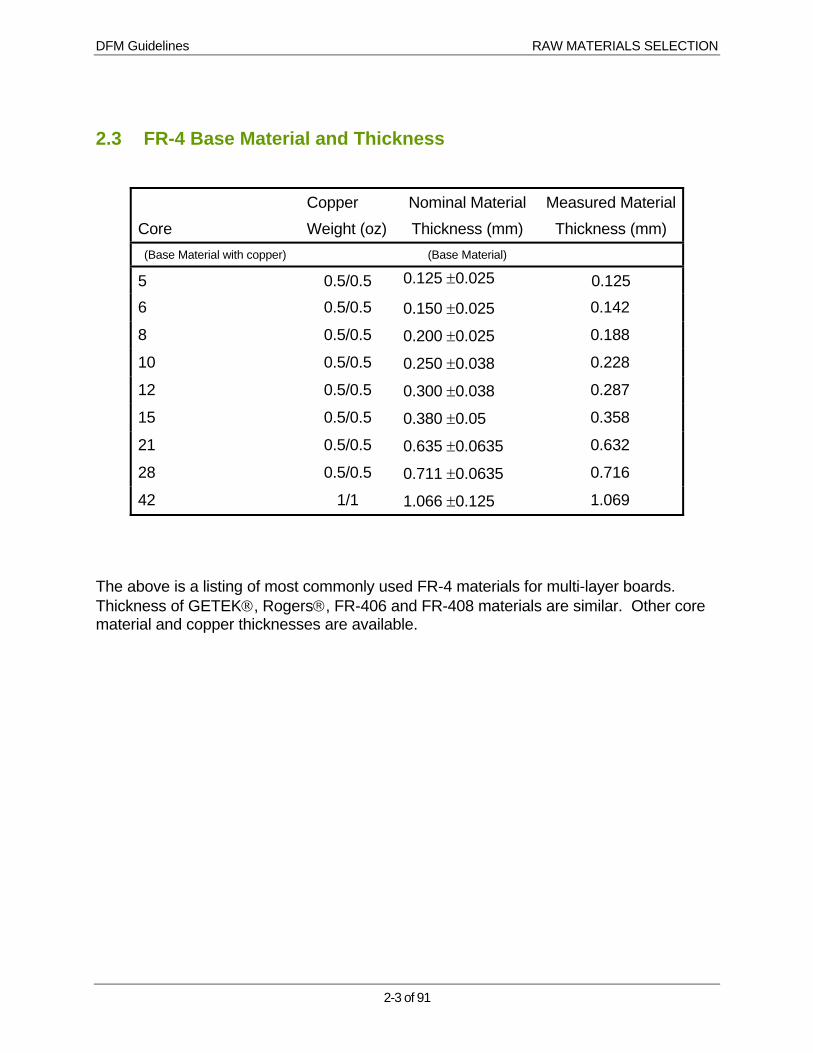
2.3 FR-4 Base Material and Thickness
Core
Copper Weight (oz)
Nominal Material Thickness (mm)
Measured MaterialThickness (mm)
(Base Material with copper) (Base Material)
5 0.5/0.5 0.125 ±0.025 0.125 6 0.5/0.5 0.150 ±0.025 0.142
8 0.5/0.5 0.200 ±0.025 0.188
10 0.5/0.5 0.250 ±0.038 0.228
12 0.5/0.5 0.300 ±0.038 0.287
15 0.5/0.5 0.380 ±0.05 0.358
21 0.5/0.5 0.635 ±0.0635 0.632
28 0.5/0.5 0.711 ±0.0635 0.716
42 1/1 1.066 ±0.125 1.069
The above is a listing of most commonly used FR-4 materials for multi-layer boards. Thickness of GETEK®, Rogers®, FR-406 and FR-408 materials are similar. Other core material and copper thicknesses are available.

DFM Guidelines RAW MATERIALS SELECTION
2-4 of 91
2.4 FR-4 Prepreg Designation and Thickness
Prepreg or “B-Stage” is the bonding material used during the construction of multi-layer boards. Most PCB manufacturers currently utilize five types of prepreg with 106, 1080, 2113, 2116 and 7628 glass styles.
Prepreg properties (after full cure) are identical to those listed for base materials on page B-2.
Due to various limitations as to the number of plies and/or types of prepreg that can be utilized between layers of a board, specific applications need to be discussed with the PCB manufacturer Application Engineering.
Pressed
Glass Style Thickness mm
106 0.053 (0.002”)
1080 0.0787 (0.003”)
2113 0.100 (0.004”)
2116 0.135 (0.005”)
7628 0.193 (0.0075”)
Thicknesses of GETEK®, Rogers®, FR-406 and FR-408 prepregs are similar. Contact the PCB manufacturer Application Engineer or Account Manager for specific data.

DFM Guidelines RAW MATERIALS SELECTION
2-5 of 91
2.5 Copper Clad for Materials
Type: Electrodeposited copper, drum side out, high-temperature-elongation.
The copper clad FR-4 material is conventionally specified by its ounce- weight per foot2.
Nominal Thickness: 0.25 oz. = 0.0035” (8.75µm) ‡
0.5 oz. = 0.007” (17.5 µm)
1.0 oz = 0.0014” (35 µm)
1.5 oz = 0.002” (53 µm)
2.0 oz = 0.0028” (70 µm)
If current carrying capacity permits, the specification of 0.5 ounce copper needs to be considered in all cases.* The advantages are:
• Reduced dimensional variation of etched features.
• Higher impedance for a given line width, less impedance variation.
• Thinner dielectric thickness for a given impedance, resulting in a thinner board.
• Reduction of copper waste generation and recycling effort by 50%. Reduced environmental impact‡.
• External layers will be electroplated with additional copper to a total thickness of 0.025mm (0.001”) minimum.
2.6 Resistivity of Copper
With designs of finer lines, distributed resistance of copper is becoming increasingly important. The formula for computing resistivity in copper traces is given by the following equation:
R = (0.679 X 10⁻⁶ ohm/inch) /(width X thickness inches X Length)
Example: In fine-line designs, using 0.5 oz. copper, a .005” trace, 5 inches long, the resistivity will be:
(.679 X 10-6) / ((5 X 0.7 X 106)) X 5 = 0.97Ω

DFM Guidelines RAW MATERIALS SELECTION
2-6 of 91
2.7 Current Carrying Capacity of Copper
The graphs are provided to reference the current carrying capacity for internal layers for common copper thickness and various temperature rises above ambient. Current carrying capacity of external layers is approximately 2X of that given for internal layers.
Cross-section (square mils)
Encapsulated Conductor
1 10 20 30 50 100 200 300 5000 5 70 400 700150
Cur
rent
(am
pere
s)
0
.5
1.0
2.0
3.0
5.0
10.0
15.0
20.0
7.0
.25
.7
12.5
10°C
20°C
30°C
45°C
Cross-section (square mils)
Conductor Width (w) vs Cross-section
1 10 20 30 50 100 200 300 5000 5 70 400 700150
1
510
2030
50
100
150
200
300
400
0
70
oz Copper (t = .0007")
12/
1 oz Copper (t = .0014")
2 oz Copper (t = .0028")Con
duct
or w
idth
(m
ils)
For detailed data on line widths and spacing requirements, see IPC-D-275 or MIL-STD-275.
DFM Guidelines RAW MATERIALS SELECTION
2-7 of 91
2.8 Panel Sizes and Usable Area
There are three preferred panel sizes, 12 x 18 inches, 16 x 18 inches, and 18 x 24 inches. Larger panel size provides the most effective cost per unit area processed. Other panel sizes are available for special applications.
Note: Processing of GETEK ® material is currently limited to a panel size 18 x 24 inches.
• The most effective material utilization will be achieved with boards or arrays of boards having their finished outline fit as efficiently as possible within the usable area of the panel‡. Test coupons must be within the usable area.
• If the entire panel is shipped to the customer, the customer may negotiate to have locating holes and/or break-away tabs for insertion or surface mount equipment located outside the usable area. This is usually accomplished via the tab-routing process.
• Material utilization may be increased by utilizing the scoring process. This process places grooves on opposite sides of the panel between boards for the purpose of snapping the boards from the panel. Since boards can be “butted up” against each other, eliminating the real-estate for route paths, more boards may be placed on the panel. This process also allows the entire panel to be shipped to the customer.

DFM Guidelines RAW MATERIALS SELECTION
2-8 of 91
2.9 Multi-layer Usable Area Diagrams
FOR MULTILAYER CIRCUIT BOARDS, A BORDER AREA OF .750 INCH AROUND THECANNOT BE USED FOR ANY PART OF THE FINISHED CIRCUIT
24”
.750” TypicallyNot Usable
Example: Usable Area of 18” x 24”
Excellent Panel Utilization (84%) Poor Panel Utilization (33%)
Panel Price $160.00Board Price $80.00
Panel Price $160.00Board Price $160.00
Example of 18” x 24” Panel Utilization
18” 16.5” X 22.5”Usable Area
11.0”
16.5”
.150Rout Path 11.0”
16.7”
DFM Guidelines RAW MATERIALS SELECTION
2-9 of 91
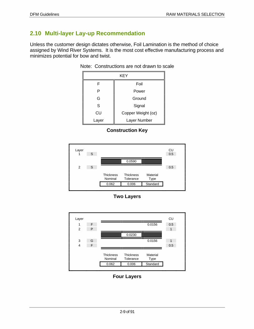
2.10 Multi-layer Lay-up Recommendation
Unless the customer design dictates otherwise, Foil Lamination is the method of choice assigned by Wind River Systems. It is the most cost effective manufacturing process and minimizes potential for bow and twist.
Note: Constructions are not drawn to scale
KEY
F Foil
P Power
G Ground
S Signal
CU Copper Weight (oz)
Layer Layer Number
Construction Key
Layer CU 1 S 0.5
⎜ 0.0590 ⎥
2 S 0.5 Thickness Thickness Material Nominal Tolerance Type 0.062 0.006 Standard
Two Layers
Layer CU
1 F 0.0156 0.5 2 P 1
⎜ 0.0230 ⎥
3 G 0.0156 1 4 F 0.5
Thickness Thickness Material Nominal Tolerance Type 0.062 0.006 Standard
Four Layers
DFM Guidelines RAW MATERIALS SELECTION
2-10 of 91
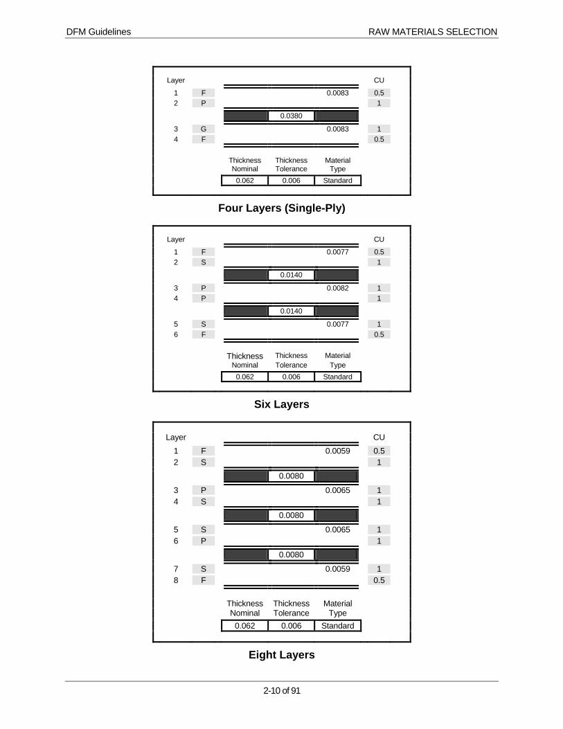
Layer CU
1 F 0.0083 0.5 2 P 1
⎜ 0.0380 ⎥
3 G 0.0083 1 4 F 0.5
Thickness Thickness Material Nominal Tolerance Type 0.062 0.006 Standard
Four Layers (Single-Ply)
Layer CU
1 F 0.0077 0.5 2 S 1
⎜ 0.0140 ⎥
3 P 0.0082 1 4 P 1
⎜ 0.0140 ⎥
5 S 0.0077 1 6 F 0.5
Thickness Thickness Material Nominal Tolerance Type 0.062 0.006 Standard
Six Layers
Layer CU 1 F 0.0059 0.5 2 S 1 ⎜ 0.0080 ⎥
3 P 0.0065 1 4 S 1 ⎜ 0.0080 ⎥
5 S 0.0065 1 6 P 1 ⎜ 0.0080 ⎥
7 S 0.0059 1 8 F 0.5 Thickness Thickness Material Nominal Tolerance Type 0.062 0.006 Standard
Eight Layers
DFM Guidelines RAW MATERIALS SELECTION
2-11 of 91
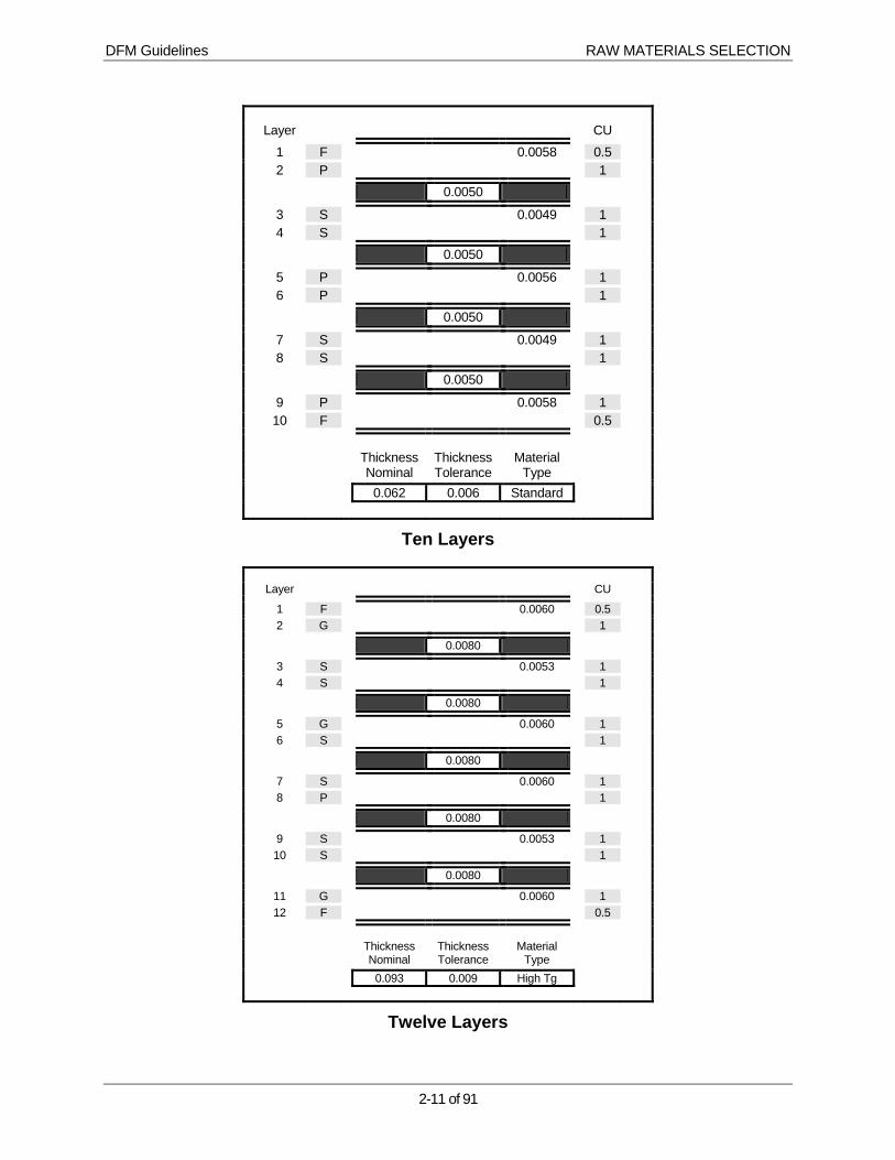
Layer CU 1 F 0.0058 0.5 2 P 1 ⎜ 0.0050 ⎥
3 S 0.0049 1 4 S 1 ⎜ 0.0050 ⎥
5 P 0.0056 1 6 P 1 ⎜ 0.0050 ⎥
7 S 0.0049 1 8 S 1 ⎜ 0.0050 ⎥
9 P 0.0058 1 10 F 0.5 Thickness Thickness Material Nominal Tolerance Type 0.062 0.006 Standard
Ten Layers
Layer CU
1 F 0.0060 0.5 2 G 1
⎜ 0.0080 ⎥
3 S 0.0053 1 4 S 1
⎜ 0.0080 ⎥
5 G 0.0060 1 6 S 1
⎜ 0.0080 ⎥
7 S 0.0060 1 8 P 1
⎜ 0.0080 ⎥
9 S 0.0053 1 10 S 1
⎜ 0.0080 ⎥
11 G 0.0060 1 12 F 0.5
Thickness Thickness Material Nominal Tolerance Type 0.093 0.009 High Tg
Twelve Layers
DFM Guidelines RAW MATERIALS SELECTION
2-12 of 91
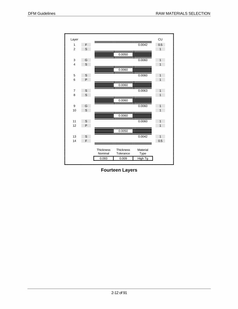
Layer CU
1 F 0.0042 0.5 2 S 1
⎜ 0.0050 ⎥
3 G 0.0060 1 4 S 1
⎜ 0.0060 ⎥
5 S 0.0060 1 6 P 1
⎜ 0.0060 ⎥
7 S 0.0063 1 8 S 1
⎜ 0.0060 ⎥
9 G 0.0060 1 10 S 1
⎜ 0.0060 ⎥
11 S 0.0060 1 12 P 1
⎜ 0.0050 ⎥
13 S 0.0042 1 14 F 0.5
Thickness Thickness Material Nominal Tolerance Type 0.093 0.009 High Tg
Fourteen Layers
DFM Guidelines RAW MATERIALS SELECTION
2-13 of 91
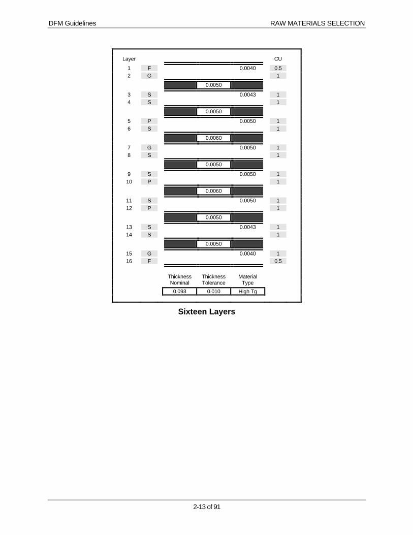
Layer CU
1 F 0.0040 0.5 2 G 1
⎜ 0.0050 ⎥
3 S 0.0043 1 4 S 1
⎜ 0.0050 ⎥
5 P 0.0050 1 6 S 1
⎜ 0.0060 ⎥
7 G 0.0050 1 8 S 1
⎜ 0.0050 ⎥
9 S 0.0050 1 10 P 1
⎜ 0.0060 ⎥
11 S 0.0050 1 12 P 1
⎜ 0.0050 ⎥
13 S 0.0043 1 14 S 1
⎜ 0.0050 ⎥
15 G 0.0040 1 16 F 0.5
Thickness Thickness Material Nominal Tolerance Type 0.093 0.010 High Tg
Sixteen Layers
DFM Guidelines RAW MATERIALS SELECTION
2-14 of 91
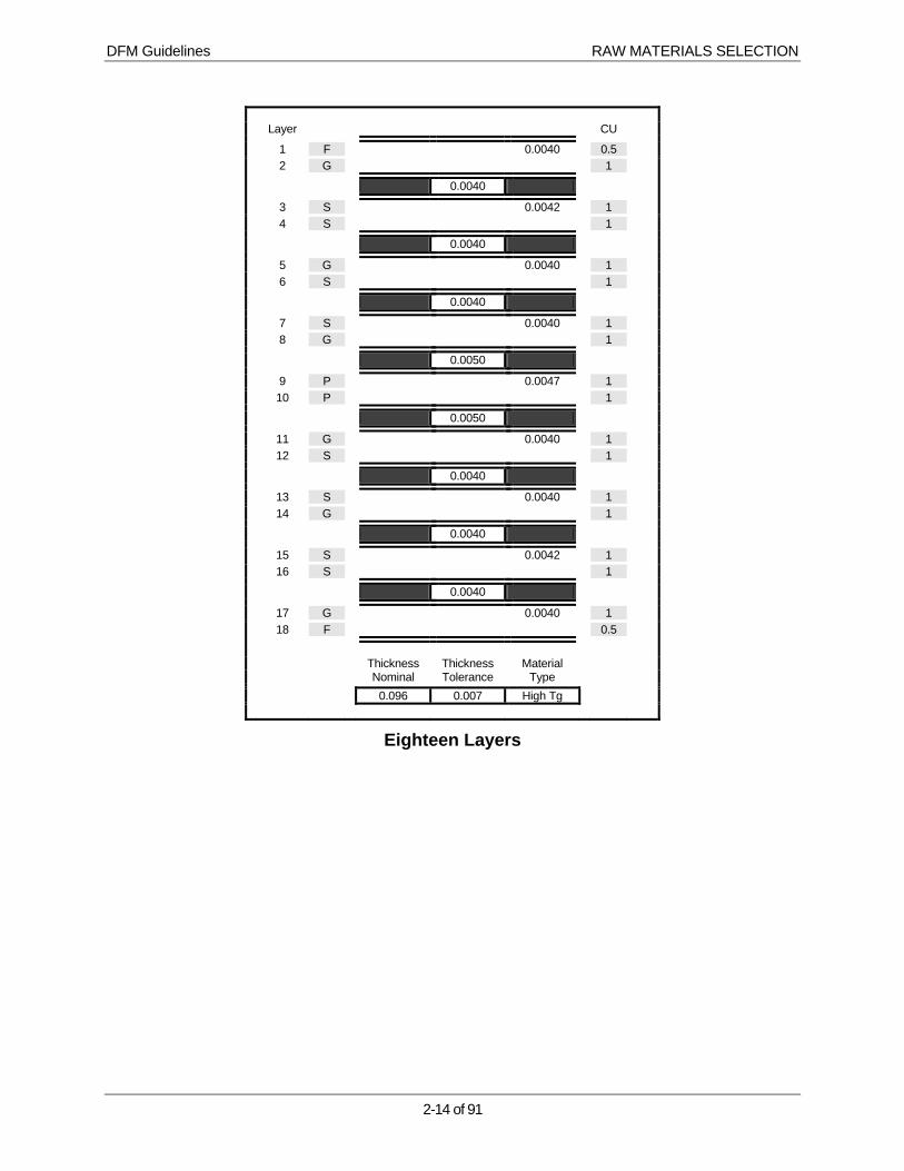
Layer CU
1 F 0.0040 0.5 2 G 1
⎜ 0.0040 ⎥
3 S 0.0042 1 4 S 1
⎜ 0.0040 ⎥
5 G 0.0040 1 6 S 1
⎜ 0.0040 ⎥
7 S 0.0040 1 8 G 1
⎜ 0.0050 ⎥
9 P 0.0047 1 10 P 1
⎜ 0.0050 ⎥
11 G 0.0040 1 12 S 1
⎜ 0.0040 ⎥
13 S 0.0040 1 14 G 1
⎜ 0.0040 ⎥
15 S 0.0042 1 16 S 1
⎜ 0.0040 ⎥
17 G 0.0040 1 18 F 0.5
Thickness Thickness Material Nominal Tolerance Type 0.096 0.007 High Tg
Eighteen Layers

DFM Guidelines RAW MATERIALS SELECTION
2-15 of 91
2.11 Recommended Lay-up for 2 – 12 Layer Boards
02A 02B 02C Layer 1 Layer 2
(Top) (Bottom)
(Top) (GND)
(GND) (Bottom)
04A 04B 04C 04D 04E 04F Layer 1 Layer 2 Layer 3 Layer 4
(Top) (GND) (PWR)
(Bottom)
(Top) (PWR) (GND)
(Bottom)
(PWR) (Signal) (Signal) (GND)
(GND) (Signal)(Signal)(PWR)
(GND) (Sig/Pwr) (Sig/Pwr) (GND)
(Top) (Signal)(Signal)(Bottom)
06A 06B 06C 06D 06E 06F 06G 06H 06J 06K Layer 1 Layer 2 Layer 3 Layer 4 Layer 5 Layer 6
(Top) (GND)
(Signal) (Signal) (PWR)
(Bottom)
(Top) (PWR) (Signal) (Signal) (GND)
(Bottom)
(Top) (Signal) (GND) (PWR) (Signal) (Bottom)
(Top) (Signal)(PWR) (GND)
(Signal)(Bottom)
(GND) (Signal)(GND) (PWR) (Signal)(GND)
(GND) (Signal)(PWR) (GND)
(Signal)(GND)
(Top) (GND)
(Signal)(PWR) (GND)
(Bottom)
(Top) (GND) (PWR) (Signal) (GND)
(Bottom)
(Top) (PWR) (GND)
(Signal)(PWR)
(Bottom)
(Top) (PWR) (Signal)(GND) (PWR)
(Bottom) 08A 08B 08C 08D 08E 08F 08G 08H 08J 08K Layer 1 Layer 2 Layer 3 Layer 4 Layer 5 Layer 6 Layer 7 Layer 8
(Top) (Signal) (GND)
(Signal) (Signal) (PWR) (Signal) (Bottom)
(Top) (Signal) (PWR) (Signal) (Signal) (GND)
(Signal) (Bottom)
(Top) (GND)
(Signal) (GND) (PWR) (Signal) (GND)
(Bottom)
(Top) (GND)
(Signal)(PWR) (GND)
(Signal)(GND)
(Bottom)
(GND) (Signal)(Signal)(GND) (PWR) (Signal)(Signal)(GND)
(GND) (Signal)(Signal)(PWR) (GND)
(Signal)(Signal)(GND)
(PWR) (Signal)(GND)
(Signal)(Signal)(PWR) (Signal)(GND)
(GND) (Signal) (PWR) (Signal) (Signal) (GND)
(Signal) (PWR)
(Top) (GND)
(Sig/Pwr)(GND)
(Sig/Pwr) (GND)
(Sig/Pwr)(Bottom)
(Top) (GND) (PWR) (Signal)(Signal)(PWR) (GND)
(Bottom) 10A 10B 10C 10D 10E 10F 10G 10H 10J 10K Layer 1 Layer 2 Layer 3 Layer 4 Layer 5 Layer 6 Layer 7 Layer 8 Layer 9 Layer 10
(Top) (GND)
(Signal) (Signal) (PWR) (GND)
(Signal) (Signal) (GND)
(Bottom)
(Top) (GND)
(Signal) (Signal) (GND) (PWR) (Signal) (Signal) (GND)
(Bottom)
(Top) (GND)
(Signal) (Signal) (PWR) (GND)
(Signal) (Signal) (PWR)
(Bottom)
(Top) (PWR) (Signal)(Signal)(GND) (PWR) (Signal)(Signal)(GND)
(Bottom)
(Top) (GND)
(Signal)(PWR) (GND)
(Signal)(PWR) (Signal)(GND)
(Bottom)
(Top) (GND)
(Signal)(PWR) (Signal)(Signal)(PWR) (Signal)(GND)
(Bottom)
(GND) (Signal)(Signal)(GND)
(Signal)(Signal)(PWR) (Signal)(Signal)(GND)
(GND) (Signal) (Signal) (PWR) (Signal) (Signal) (GND)
(Signal) (Signal) (GND)
(GND) (Signal)(GND) (PWR) (Signal)(Signal)(GND) (PWR) (Signal)(GND)
(GND) (Signal)(PWR) (GND)
(Signal)(Signal)(GND) (PWR) (Signal)(GND)
12A 12B 12C 12D 12E 12F 12G 12H 12J 12K Layer 1 Layer 2 Layer 3 Layer 4 Layer 5 Layer 6 Layer 7 Layer 8 Layer 9 Layer 10 Layer 11 Layer 12
(Top) (GND) (PWR) (Signal) (Signal) (GND) (PWR) (Signal) (Signal) (GND) (PWR)
(Bottom)
(Top) (PWR) (GND)
(Signal) (Signal) (PWR) (GND)
(Signal) (Signal) (PWR) (GND)
(Bottom)
(Top) (GND)
(Signal) (PWR) (Signal) (GND) (PWR) (Signal) (PWR) (Signal) (GND)
(Bottom)
(Top) (GND)
(Signal)(GND)
(Signal)(PWR) (GND)
(Signal)(PWR) (Signal)(GND)
(Bottom)
(Top) (GND)
(Signal)(Signal)(PWR) (Signal)(Signal)(GND)
(Signal)(Signal)(GND)
(Bottom)
(Top) (GND)
(Signal)(Signal)(GND)
(Signal)(Signal)(PWR) (Signal)(Signal)(GND)
(Bottom)
(Top) (GND)
(Signal)(Signal)(PWR) (Signal)(Signal)(GND)
(Signal)(Signal)(PWR)
(Bottom)
(Top) (PWR) (Signal) (Signal) (GND)
(Signal) (Signal) (PWR) (Signal) (Signal) (GND)
(Bottom)
(GND) (Signal)(Signal)(PWR) (GND)
(Signal)(Signal)(PWR) (GND)
(Signal)(Signal)(GND)
(Top) (GND)
(Signal)(Signal)(PWR) (GND)
(Signal)(Signal)(GND)
(Signal)(Signal)(GND)
DFM Guidelines RAW MATERIALS SELECTION
2-16 of 91
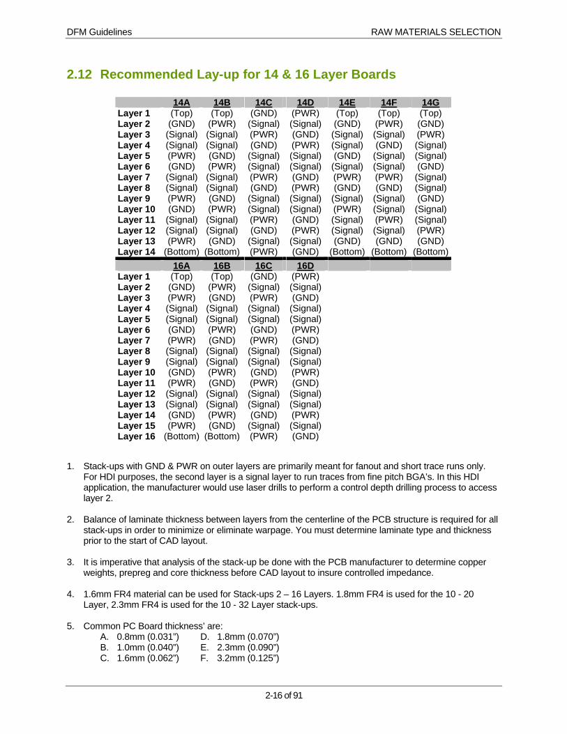
2.12 Recommended Lay-up for 14 & 16 Layer Boards
14A 14B 14C 14D 14E 14F 14G Layer 1 Layer 2 Layer 3 Layer 4 Layer 5 Layer 6 Layer 7 Layer 8 Layer 9 Layer 10 Layer 11 Layer 12 Layer 13 Layer 14
(Top) (GND) (Signal) (Signal) (PWR) (GND) (Signal) (Signal) (PWR) (GND) (Signal) (Signal) (PWR)
(Bottom)
(Top) (PWR) (Signal) (Signal) (GND) (PWR) (Signal) (Signal) (GND) (PWR) (Signal) (Signal) (GND)
(Bottom)
(GND) (Signal) (PWR) (GND)
(Signal) (Signal) (PWR) (GND)
(Signal) (Signal) (PWR) (GND)
(Signal) (PWR)
(PWR) (Signal) (GND) (PWR) (Signal) (Signal) (GND) (PWR) (Signal) (Signal) (GND) (PWR) (Signal) (GND)
(Top) (GND)
(Signal) (Signal) (GND)
(Signal) (PWR) (GND)
(Signal) (PWR) (Signal) (Signal) (GND)
(Bottom)
(Top) (PWR) (Signal) (GND)
(Signal) (Signal) (PWR) (GND)
(Signal) (Signal) (PWR) (Signal) (GND)
(Bottom)
(Top) (GND) (PWR) (Signal) (Signal) (GND)
(Signal) (Signal) (GND)
(Signal) (Signal) (PWR) (GND)
(Bottom) 16A 16B 16C 16D Layer 1 Layer 2 Layer 3 Layer 4 Layer 5 Layer 6 Layer 7 Layer 8 Layer 9 Layer 10 Layer 11 Layer 12 Layer 13 Layer 14 Layer 15 Layer 16
(Top) (GND) (PWR) (Signal) (Signal) (GND) (PWR) (Signal) (Signal) (GND) (PWR) (Signal) (Signal) (GND) (PWR)
(Bottom)
(Top) (PWR) (GND)
(Signal) (Signal) (PWR) (GND)
(Signal) (Signal) (PWR) (GND)
(Signal) (Signal) (PWR) (GND)
(Bottom)
(GND) (Signal) (PWR) (Signal) (Signal) (GND) (PWR) (Signal) (Signal) (GND) (PWR) (Signal) (Signal) (GND)
(Signal) (PWR)
(PWR) (Signal) (GND)
(Signal) (Signal) (PWR) (GND)
(Signal) (Signal) (PWR) (GND)
(Signal) (Signal) (PWR) (Signal) (GND)
1. Stack-ups with GND & PWR on outer layers are primarily meant for fanout and short trace runs only.
For HDI purposes, the second layer is a signal layer to run traces from fine pitch BGA’s. In this HDI application, the manufacturer would use laser drills to perform a control depth drilling process to access layer 2.
2. Balance of laminate thickness between layers from the centerline of the PCB structure is required for all
stack-ups in order to minimize or eliminate warpage. You must determine laminate type and thickness prior to the start of CAD layout.
3. It is imperative that analysis of the stack-up be done with the PCB manufacturer to determine copper
weights, prepreg and core thickness before CAD layout to insure controlled impedance. 4. 1.6mm FR4 material can be used for Stack-ups 2 – 16 Layers. 1.8mm FR4 is used for the 10 - 20
Layer, 2.3mm FR4 is used for the 10 - 32 Layer stack-ups. 5. Common PC Board thickness’ are:
A. 0.8mm (0.031”) D. 1.8mm (0.070”) B. 1.0mm (0.040”) E. 2.3mm (0.090”) C. 1.6mm (0.062”) F. 3.2mm (0.125”)
DFM Guidelines RAW MATERIALS SELECTION
2-17 of 91
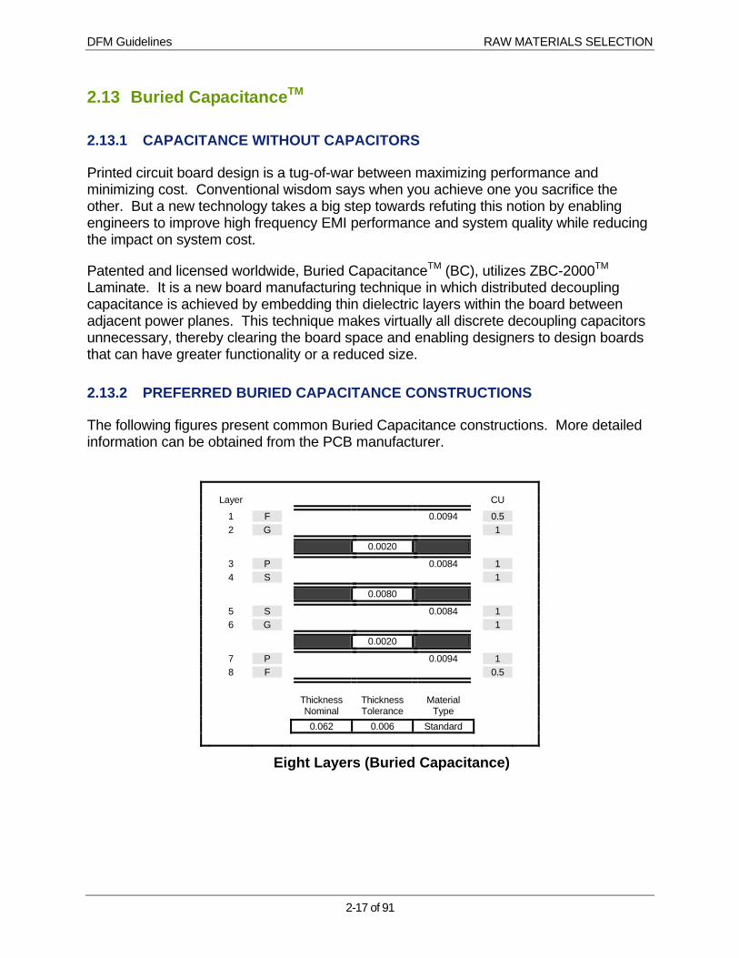
2.13 Buried CapacitanceTM
2.13.1 CAPACITANCE WITHOUT CAPACITORS
Printed circuit board design is a tug-of-war between maximizing performance and minimizing cost. Conventional wisdom says when you achieve one you sacrifice the other. But a new technology takes a big step towards refuting this notion by enabling engineers to improve high frequency EMI performance and system quality while reducing the impact on system cost.
Patented and licensed worldwide, Buried CapacitanceTM (BC), utilizes ZBC-2000TM Laminate. It is a new board manufacturing technique in which distributed decoupling capacitance is achieved by embedding thin dielectric layers within the board between adjacent power planes. This technique makes virtually all discrete decoupling capacitors unnecessary, thereby clearing the board space and enabling designers to design boards that can have greater functionality or a reduced size.
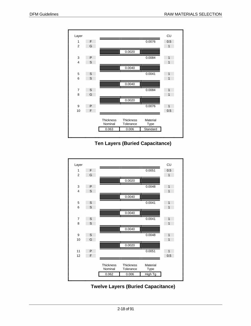
2.13.2 PREFERRED BURIED CAPACITANCE CONSTRUCTIONS
The following figures present common Buried Capacitance constructions. More detailed information can be obtained from the PCB manufacturer.
Layer CU
1 F 0.0094 0.5 2 G 1
⎜ 0.0020 ⎥
3 P 0.0084 1 4 S 1
⎜ 0.0080 ⎥
5 S 0.0084 1 6 G 1
⎜ 0.0020 ⎥
7 P 0.0094 1 8 F 0.5
Thickness Thickness Material Nominal Tolerance Type 0.062 0.006 Standard
Eight Layers (Buried Capacitance)
DFM Guidelines RAW MATERIALS SELECTION
2-18 of 91
Layer CU
1 F 0.0076 0.5 2 G 1
⎜ 0.0020 ⎥
3 P 0.0084 1 4 S 1
⎜ 0.0040 ⎥
5 S 0.0041 1 6 S 1
⎜ 0.0040 ⎥
7 S 0.0084 1 8 G 1
⎜ 0.0020 ⎥
9 P 0.0076 1 10 F 0.5
Thickness Thickness Material Nominal Tolerance Type 0.063 0.006 Standard
Ten Layers (Buried Capacitance)
Layer CU
1 F 0.0051 0.5 2 G 1
⎜ 0.0020 ⎥
3 P 0.0048 1 4 S 1
⎜ 0.0040 ⎥
5 S 0.0041 1 6 S 1
⎜ 0.0040 ⎥
7 S 0.0041 1 8 S 1
⎜ 0.0040 ⎥
9 S 0.0048 1 10 G 1
⎜ 0.0020 ⎥
11 P 0.0051 1 12 F 0.5
Thickness Thickness Material Nominal Tolerance Type 0.062 0.006 High Tg
Twelve Layers (Buried Capacitance)
DFM Guidelines RAW MATERIALS SELECTION
2-19 of 91
2.14 Multi-layer Lay-up
1. Design multi-layer boards with an even number of layers.
2. If specifying dielectric thickness, as may be required for impedance reasons for example, the dimensions should be selected from core or prepreg thicknesses that are available from the PCB manufacturer.
Dielectric thicknesses made up of prepreg depend on the type or the combination of different types of these materials. The PCB manufacturer will advise Wind River Systems of what combination of prepreg is suitable and of achievable dimensions and tolerances.
It is beneficial to discuss special dielectric requirements with the PCB manufacturer during the design stage if possible. This will allow time for material procurement if necessary. Also, manufacturing concerns can be addressed while an opportunity still exists to make changes.
Note: Thickness is not the only indicator of material cost. Other factors, such as number of plies used, material type, thickness tolerance, or the demand for this material may influence cost. If no specific dielectric thicknesses are required, it is best to allow the PCB manufacturer to make the material selection. Materials that meet industry standards, are of lowest cost, and allow the most effective manufacturing methods will be utilized.
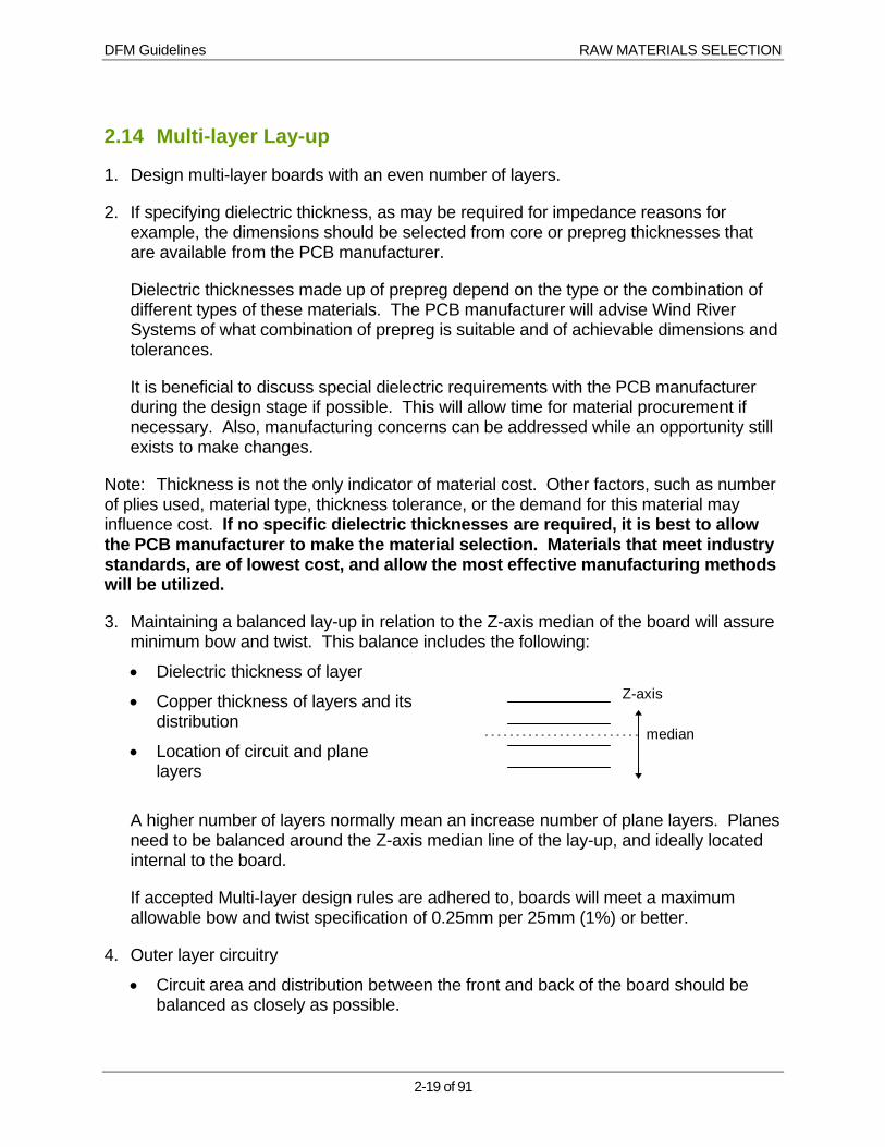
3. Maintaining a balanced lay-up in relation to the Z-axis median of the board will assure minimum bow and twist. This balance includes the following:
• Dielectric thickness of layer
• Copper thickness of layers and its distribution
• Location of circuit and plane layers
median
Z-axis
A higher number of layers normally mean an increase number of plane layers. Planes need to be balanced around the Z-axis median line of the lay-up, and ideally located internal to the board.
If accepted Multi-layer design rules are adhered to, boards will meet a maximum allowable bow and twist specification of 0.25mm per 25mm (1%) or better.
4. Outer layer circuitry
• Circuit area and distribution between the front and back of the board should be balanced as closely as possible.
DFM Guidelines RAW MATERIALS SELECTION
2-2 of 91
• Plating thieving of low pattern density of external plane area should be considered.
5. Thickness Tolerance
• As the overall thickness of a multi-layer board increases, the thickness tolerance should also increase. A good rule is to specify a tolerance of ±10% of the overall thickness.
• Always indicate where the thickness measurement is to be taken. Examples might be: glass to glass at rail guides, over gold contacts, over solder mask, etc.
When calculating the potential board thickness, consideration needs to be given to certain design characteristics. An example would be: Have the plane layers been pulled back from under the gold contacts? In that case, do not add the copper thickness of the planes to the board thickness, if measured across contacts.
NOTE: The contribution that the copper thickness of signal and plane layers make to the thickness of the board depends on the width and density of signal lines and the open area of planes. An isolated 0.15mm line may totally embed itself into the prepreg and make no contribution to the thickness of the board. Talk with Wind River Systems if the overall thickness is of overriding importance. The needed overall thickness tolerance is primarily based on statistical material measurement data. The ±10% is a general recommendation. Depending on the multi-layer lay-up structure and materials used, a closer tolerance is often achievable. Such a requirement needs to be discussed with the PCB manufacturer for appropriate focus.
2.15 Fabrication Drawing
The designer needs to specify the critical features of the design
• Layer Stack-up with finished board thickness and layer quantity
• Dielectric Spacing
• Drill Chart
• Dimensioned Board Outline
• Impedance Requirements
• Blind and Buried Via instructions
The fabrication drawing should contain any electrical performance characteristic critical to the manufacture of the board. The PCB fabricator should be left with the maximum amount of latitude the design will allow.
DFM Guidelines COMPLEXITY FACTOR CLASSIFICATION
3-1 of 91
3 COMPLEXITY FACTOR CLASSIFICATION
3.1 Objective
To communicate rules and guidelines for the design of high density printed circuit boards using the “Complexity Factor Matrix" to ensure optimum manufacturability.
The "Complexity Factor Matrix" enables circuit board designers to assess the impact of a board's key characteristics on manufacturing. By understanding the Matrix and the rules and guidelines, one can improve board yield, which ultimately impacts quality, delivery, price, and environmental impact.
These parameters are preferred by PCB manufacturers. Others may be considered but may result in lower yield and higher board prices.
All new parts will be screened against the stated manufacturing capabilities either the first time they are built or whenever a change is made to the part number.
The Technical Support/Application Engineering group evaluates key design characteristics to determine what level of complexity a given board design represents.
The “Complexity Factor Matrix” (see section 3.2) has been developed to use as a tool in classifying parts. The matrix is structured with board characteristics located down the left-hand side, manufacturing areas impacted along the top, and the tolerances allowed for those characteristics are located down the right-hand side.
By using the matrix, one can make an initial assessment of the impact of a design’s characteristics on the manufacturing areas, and ultimately the price of the circuit board.
Board Producibility Levels
These levels reflect progressive increases in sophistication of design, tooling, materials and processing and, therefore progressive increases in fabrication cost. These levels are:
Class 1 General design complexity. Components typically placed on 1mm grid. Designed trace width and spacing 0.2mm or more.
Class 2 Moderate or standard design complexity. Components placed on 0.5mm grid. Maximum of two traces between IC lands. Designed trace width and spacing 0.125mm to 0.15mm.
Class 3 High design complexity (surface mount pads of 0.4mm or 0.5mm pitch). Components placed on 0.1mm grid, with traces and spacing 0.075mm to 0.1mm. This class may require special handling or process controls.

DFM Guidelines COMPLEXITY FACTOR CLASSIFICATION
3-2 of 91
3.2 Complexity Factors Matrix
CATEGORY INN DRI LAM OUT PLA SM FIN DIMENSIONS (mm) Trace Width
1 2 3 4
1 2 3 4
3 4
GE 0.175 GE 0.1 & LT 0.175 GE 0.075 & LE 0.1 LT 0.075
Space Width
1 2 3
1 2 3
3 4
GE 0.175 GE 0.1 & LT 0.175 GE 0.075 & LE 0.1 LT 0.075
Annular Ring Radius
1 2 3 4
1 2 3 4
1 2 3 4
1 2 3 4
GE 0.216 GE 0.125 & LT 0.216GE 0.1 & LT 0.165 LT 0.1
Clearance Pad Radius
1 2 3 4
1 2 3 4
GT 0.47 GE 0.45 GE 0.25 & LT 0.35 LT 0.25
Overall Profile Tolerance
1 2 3 4
GT ± 0.2 GT ± 0.1 & LT ± 0.2 EQ ± 0.1 LT ± 0.1
Finished Hole Tolerance
GE ± 0.075 HASL GE ± 0.05 No HASL
Finished Board Thickness
See section 3.12
Aspect Ratio See section 3.13
Key: INN - Inner Layer PLA – Plating GE - Greater Than or Equal To DRI - Drilling SM - Solder Mask LT - Less Than LAM - ML Lamination FIN - Finishing (Profiling) LE - Less Than or Equal To OUT - Outer Layer GT - Greater Than EQ - Equal To Note: All dimensions are in millimeters
DFM Guidelines COMPLEXITY FACTOR CLASSIFICATION
3-3 of 91
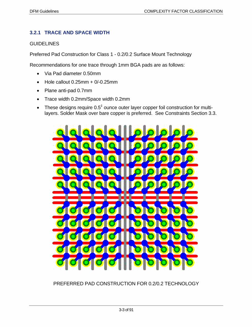
3.2.1 TRACE AND SPACE WIDTH
GUIDELINES
Preferred Pad Construction for Class 1 - 0.2/0.2 Surface Mount Technology
Recommendations for one trace through 1mm BGA pads are as follows:
• Via Pad diameter 0.50mm
• Hole callout 0.25mm + 0/-0.25mm
• Plane anti-pad 0.7mm
• Trace width 0.2mm/Space width 0.2mm
• These designs require 0.5‡ ounce outer layer copper foil construction for multi-layers. Solder Mask over bare copper is preferred. See Constraints Section 3.3.
PREFERRED PAD CONSTRUCTION FOR 0.2/0.2 TECHNOLOGY
DFM Guidelines COMPLEXITY FACTOR CLASSIFICATION
3-4 of 91
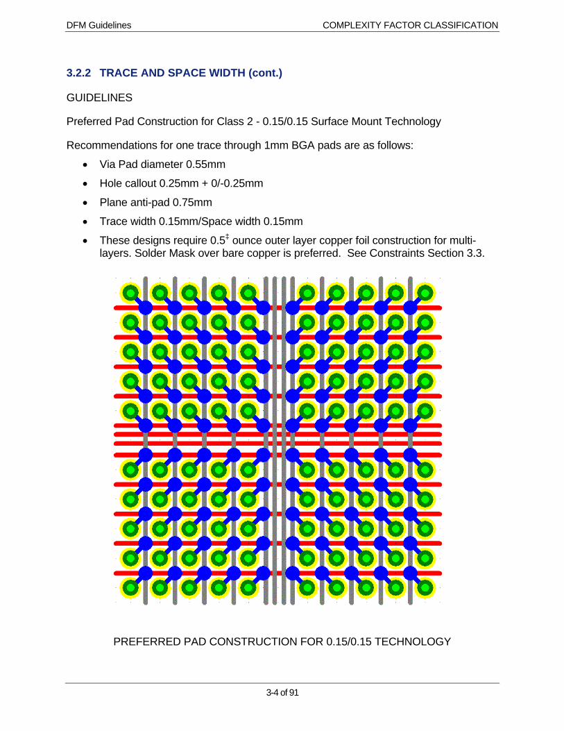
3.2.2 TRACE AND SPACE WIDTH (cont.)
GUIDELINES
Preferred Pad Construction for Class 2 - 0.15/0.15 Surface Mount Technology
Recommendations for one trace through 1mm BGA pads are as follows:
• Via Pad diameter 0.55mm
• Hole callout 0.25mm + 0/-0.25mm
• Plane anti-pad 0.75mm
• Trace width 0.15mm/Space width 0.15mm
• These designs require 0.5‡ ounce outer layer copper foil construction for multi-layers. Solder Mask over bare copper is preferred. See Constraints Section 3.3.
PREFERRED PAD CONSTRUCTION FOR 0.15/0.15 TECHNOLOGY

DFM Guidelines COMPLEXITY FACTOR CLASSIFICATION
3-5 of 91
3.2.3 TRACE AND SPACE WIDTH (cont.)
GUIDELINES
Preferred Pad Construction for Class 3 – 0.125/0.125 Surface Mount Technology
Recommendations for two traces between 1mm BGA pads are as follows:
• Via Pad diameter 0.55mm
• Hole callout 0.25mm +0/-0.25mm
• Plane anti-pad 0.75mm
• Trace width 0.125mm / Space width 0.125mm
• Route grid 0.05mm
• These designs require 0.5‡ ounce outer layer copper foil construction for multi-layers. Solder Mask over bare copper is preferred. See Constraints Section 3.3.
PREFERRED PAD CONSTRUCTION FOR 0.125/0.125 TECHNOLOGY

DFM Guidelines COMPLEXITY FACTOR CLASSIFICATION
3-6 of 91
3.2.4 TRACE AND SPACE WIDTH (cont.)
GUIDELINES
Preferred Pad Construction for Class 3 – 0.1/0.1 Surface Mount Technology
Recommendations for two traces between 1mm BGA pads are as follows:
• Pad diameter 0.5mm
• Hole callout 0.25mm + 0/-0.25mm
• Plane anti-pad 0.70mm
• Route grid 0.1mm
• Trace width 0.1mm / Space width 0.1mm
These designs require 0.5‡ ounce outer layer and inner layer copper construction for multi-layers. Solder Mask over bare copper is preferred.
PREFERRED PAD CONSTRUCTION FOR 0.1/0.1 TECHNOLOGY
DFM Guidelines COMPLEXITY FACTOR CLASSIFICATION
3-7 of 91
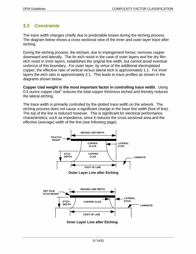
3.3 Constraints
The trace width changes chiefly due to predictable losses during the etching process. The diagram below shows a cross sectional view of the inner and outer layer trace after etching.
During the etching process, the etchant, due to impingement forces, removes copper downward and laterally. The tin etch resist in the case of outer layers and the dry film etch resist in inner layers, establishes the original line width, but cannot avoid eventual undercut of this boundary. For outer layer, by virtue of the additional electroplated copper, the effective ratio of vertical versus lateral etch is approximately 1:1. For inner layers the etch ratio is approximately 2:1. This leads to trace profiles as shown in the diagrams shown below.
Copper clad weight is the most important factor in controlling trace width. Using 0.5 ounce copper clad‡ reduces the total copper thickness etched and thereby reduces the lateral etching.
The trace width is primarily controlled by the plotted trace width on the artwork. The etching process does not cause a significant change in the base line width (foot of line). The top of the line is reduced however. This is significant for electrical performance characteristics, such as impedance, since it reduces the cross sectional area and the effective (average) width of the line (see following page).
COPPER PLATE
ETCHDEPTH
LATERALETCH
COPPER CLAD
TIN ETCH RESIST
IMAGED LINE WIDTH
FOOT OF LINE
LAMINATE
Outer Layer Line after Etching
COPPER CLAD
DRY FILMETCH RESIST
IMAGED LINE WIDTH
LATERALETCH
FOOT OF LINE
LAMINATEETCHDEPTH
Inner Layer Line after Etching
DFM Guidelines COMPLEXITY FACTOR CLASSIFICATION
3-8 of 91
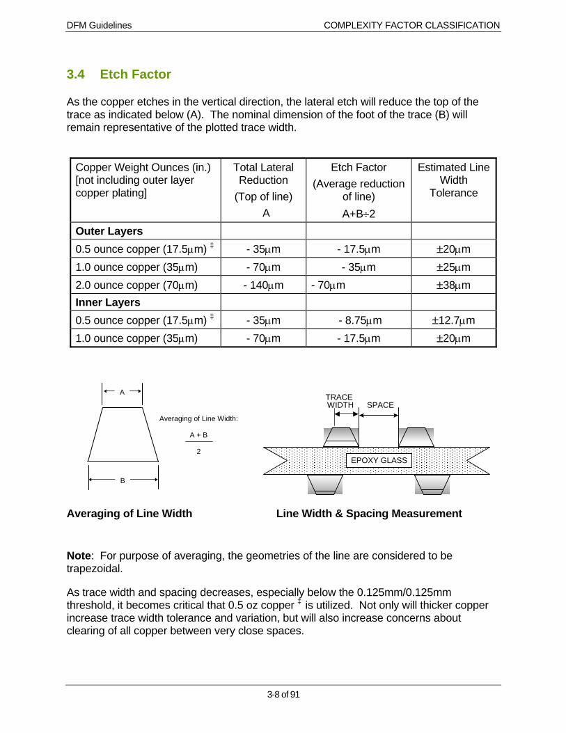
3.4 Etch Factor
As the copper etches in the vertical direction, the lateral etch will reduce the top of the trace as indicated below (A). The nominal dimension of the foot of the trace (B) will remain representative of the plotted trace width.
Copper Weight Ounces (in.) [not including outer layer copper plating]
Total Lateral Reduction
(Top of line) A
Etch Factor (Average reduction
of line) A+B÷2
Estimated Line Width
Tolerance
Outer Layers 0.5 ounce copper (17.5µm) ‡ - 35µm - 17.5µm ±20µm 1.0 ounce copper (35µm) - 70µm - 35µm ±25µm 2.0 ounce copper (70µm) - 140µm - 70µm ±38µm Inner Layers 0.5 ounce copper (17.5µm) ‡ - 35µm - 8.75µm ±12.7µm 1.0 ounce copper (35µm) - 70µm - 17.5µm ±20µm
Averaging of Line Width:
A + B
2
A
B
EPOXY GLASS
WIDTH SPACE TRACE
Averaging of Line Width Line Width & Spacing Measurement
Note: For purpose of averaging, the geometries of the line are considered to be trapezoidal.
As trace width and spacing decreases, especially below the 0.125mm/0.125mm threshold, it becomes critical that 0.5 oz copper ‡ is utilized. Not only will thicker copper increase trace width tolerance and variation, but will also increase concerns about clearing of all copper between very close spaces.

DFM Guidelines COMPLEXITY FACTOR CLASSIFICATION
3-9 of 91
3.5 Plated Finished Hole Tolerance
The finished plated hole tolerance as specified on the drawing.
3.5.1 RULES TO AVOID CLASS 4:
No tighter than ±0.05mm (0.002”) on the finished plated hole size (complexity factor 3). Both finished hole size and tolerance become an issue when mixed technology (designs with both surface mount and through hole technology) is used on Hot-Air-Solder-Leveled boards. Holes which are drilled with less than a 0.6mm (0.024”) drill may plug with solder.
3.5.2 CONSTRAINTS
Ability to control additive tolerances occurring in drilling, copper plating and Hot-Air-Solder-Leveling.
3.5.3 UNPLATED FINISHED HOLE DIAMETER TOLERANCES
Feature Size in Millimeters Method In Millimeters
0.8 to 1.6
1.65 to 5.0
5.05 to 6.75
Drill
Drill
Drill
± 0.025
+0.05 / -0.025
± 0.125
> 6.75 Route ± 0.125
> 6.75 Nibble Drill ± 0.08

DFM Guidelines COMPLEXITY FACTOR CLASSIFICATION
3-10 of 91
3.6 Unplated Drilled Slot Size Tolerance
A slot feature is formed during the drilling process. A series of overlapping holes are drilled in a manner that produces a slot of variable length and width. These techniques are applicable to primary or secondary drilling operations. The slot length is controlled by the NC program and the slot width is established by the drill diameter.
Tolerances for length and width of slot
Straight Slot (Non-Intersecting Slot)
Intersecting Slot (‘L’ Slot, ‘T’ Slot, etc.)
Length <= 2 x Width Length > 2 x Width Length <= 2 x Width Length > 2 x Width
1.65 <Diameter +/- 0.08mm +/- 0.05mm +/- 0.08mm +/- 0.05mm
1.15 <Dia <=1.65 +/- 0.15mm +/- 0.05mm +/- 0.15mm +/- 0.05mm
0.8 <=Dia <=1.15 X +/- 0.08mm X +/- 0.1mm
Diameter <0.8mm X X X X
Positional Tolerance
All Holes drilled at the primary sequence will be within 0.15mm (0.006”) of diametrical true position. The hole location tolerance for those holes drilled at a secondary drilling operation is 0.35mm (0.014”) true position referenced from a primary hole datum.
3.6.1 CONSTRAINTS
Secondary drilling through plated surface features produces burrs and results in excessive hand finish work.

DFM Guidelines COMPLEXITY FACTOR CLASSIFICATION
3-11 of 91
3.7 Minimum and Maximum Drill Diameter
The minimum drill diameter is the smallest specified or selected drill diameter based on customer requirements. Expense associated with drilling can be the second largest cost component of a printed circuit board. Number of drill hits, stack height, and number of different drills selected are critical components of drilling. The number of boards that can be drilled in one set up (stack height) is determined by minimum drill diameter, registration tolerances, and board thickness.
3.7.1 RULES TO AVOID CLASS 4:
• No smaller than 0.20mm diameter drill (for a finished plated hole tolerance of +0.00/-0.2*). Aspect Ratio must be taken into consideration when selecting minimum drill size. See section 3.13
• Maximum hole size is 6.75mm. Holes 4mm or larger require pilot drilling.
3.7.2 CONSTRAINTS
The minimum drill diameter is determined by our plating capability. See Aspect Ratio section 3.13.
* Via holes of less than 0.5mm drill diameter will probably remain plugged after HASL. No minus tolerance specified.

DFM Guidelines COMPLEXITY FACTOR CLASSIFICATION
3-12 of 91
3.8 Drill Selection
Available drill sizes are listed below. For holes plated with copper and hot air leveled, a drill size will be chosen that is 0.125mm to 0.15mm larger than the specified nominal finished hole size. For those holes which will only receive copper plating and organic coating, and no hot air leveled solder, a drill size will be chosen that is 0.075mm to 0.1mm larger than the specified nominal finished hole size.
.0087 90
.0100 87
.0120 83
.0135 80
.0145 79
.0160 78
.0180 77
.0200 76
.0210 75
.0225 74
.0240 73
.0250 72
.0260 71
.0280 70
.0292 69
.0310 68
.0320 67
.0330 66
.0350 65
.0360 64
.0370 63
.0380 62
.0390 61
.0400 60
.0410 59
.0420 58
.0430 57
.0453 1.15mm
.0465 56
.0472 1.20mm
.0492 1.25mm
.0512 1.30mm
.0520 55
.0531 1.35mm
.0550 54
.0571 1.45mm
.0595 53
.0610 1.55mm
.0625 1/16
.0635 52
.0650 1.65mm
.0670 51
.0689 1.75mm
.0700 50
.0709 1.80mm
.0728 1.85mm
.0748 1.90mm
.0760 48
.0768 1.95mm
.0785 47
.0810 46
.0820 45
.0827 2.10mm
.0846 2.15mm
.0860 44
.0866 2.20mm
.0890 43
.0906 2.30mm
.0925 2.35mm
.0935 42
.0945 2.40mm
.0960 41
.0980 40
.0995 39
.1015 38
.1024 2.60mm
.1040 37
.1065 36
.1083 2.75mm
.1094 7/64
.1100 35
.1110 34
.1122 2.85mm
.1130 33
.1160 32
.1181 3.00mm
.1200 31
.1220 3.10mm
.1240 3.15mm
.1250 1/8
.1260 3.20mm
.1280 3.25mm
.1285 30
.1299 3.30mm
.1319 3.35mm
.1339 3.40mm
.1360 29
.1378 3.50mm
.1405 28
.1417 3.60mm
.1440 27
.1457 3.70mm
.1470 26
.1495 25
.1520 24
.1540 23
.1555 3.95mm
.1570 22
.1590 21
.1610 20
.1634 4.15mm
.1654 4.20mm
.1660 19
.1673 4.25mm
.1695 18
.1719 11/64
.1730 17
.1752 4.45mm
.1770 16
.1800 15
.1811 14
.1820 14
.1830 4.65mm
.1850 13
.1875 3/16
.1890 12
.1910 11
.1935 10
.1960 9
.1990 8
.2010 7
.2031 13/64
.2040 6
.2055 5
.2090 4
.2130 3
.2165 5.50mm
.2188 7/32
.2210 2
.2264 5.75mm
.2280 1
.2323 5.90mm
.2340 A
.2362 6.00mm
.2380 B
.2402 6.10mm
.2441 6.20mm
.2460 D
.2480 6.30mm
.2500 1/4
.2520 6.40mm
.2559 6.50mm
.2570 F
.2610 G
.2638 6.70mm
.2660 H
(inches) (inches) (inches) (inches)
Available Drills
DFM Guidelines COMPLEXITY FACTOR CLASSIFICATION
3-13 of 91
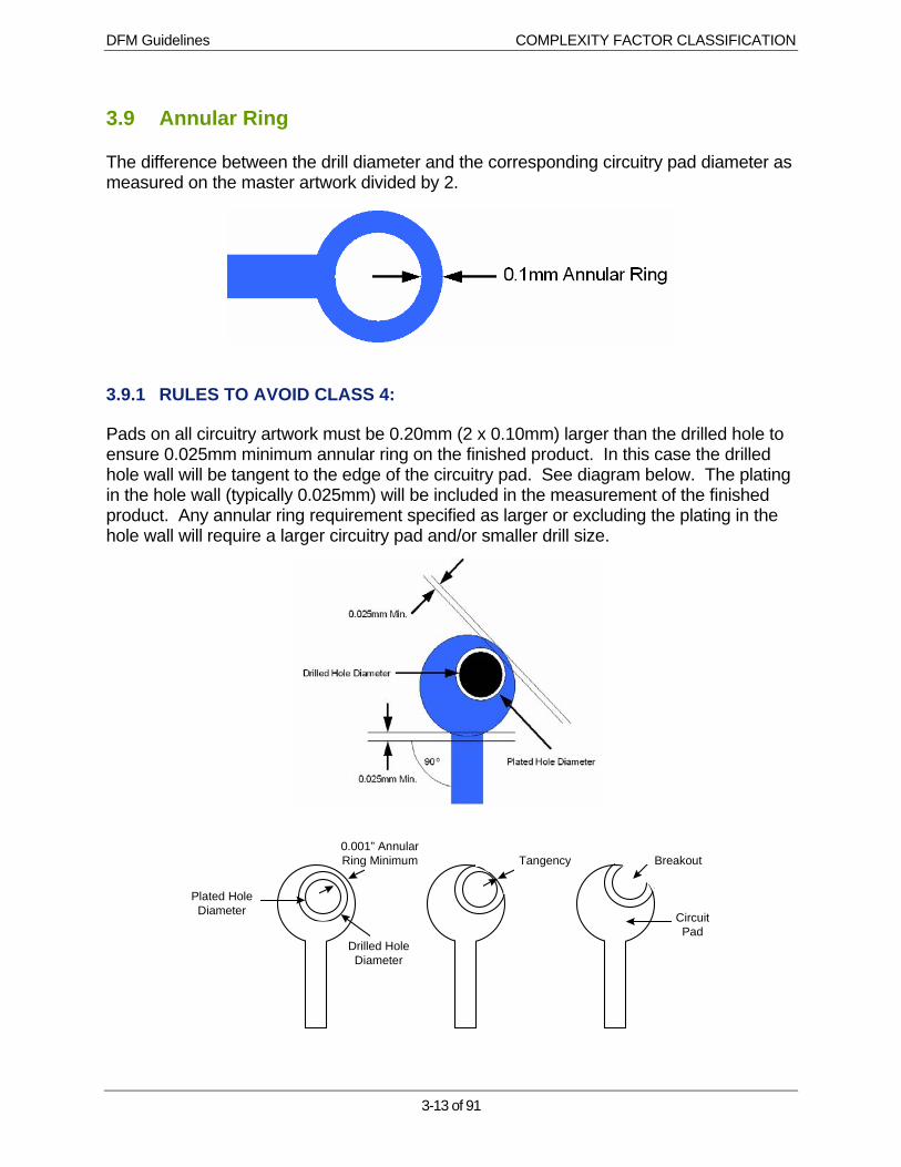
3.9 Annular Ring
The difference between the drill diameter and the corresponding circuitry pad diameter as measured on the master artwork divided by 2.
3.9.1 RULES TO AVOID CLASS 4:
Pads on all circuitry artwork must be 0.20mm (2 x 0.10mm) larger than the drilled hole to ensure 0.025mm minimum annular ring on the finished product. In this case the drilled hole wall will be tangent to the edge of the circuitry pad. See diagram below. The plating in the hole wall (typically 0.025mm) will be included in the measurement of the finished product. Any annular ring requirement specified as larger or excluding the plating in the hole wall will require a larger circuitry pad and/or smaller drill size.
0.001” Annular
Plated HoleDiameter
Drilled HoleDiameter
Ring Minimum Tangency
CircuitPad
Breakout

DFM Guidelines COMPLEXITY FACTOR CLASSIFICATION
3-14 of 91
Annular Ring / Tangency / Breakout 3.10 Tear Drop Pads
This process is designed to provide additional metal at the critical junction of a pad and a run. When an order is drilled and misregistration occurs, it has been theorized that a long-term reliability issue can arise if the misregistration occurs at the junction of the pad and the trace. Adding metal at this location helps ensure that an adequate connection is made and maintained.
The tear dropping process involves adding secondary pads at the junction of an existing (primary) pad and a circuit run. These secondary pads are sized 0.05mm smaller than the primary pads, and the center is placed 0.075mm away from the center of the primary pad.
This tooling process is conducted using IPC standards for tear dropping and has proven to be highly reliable and effective.
TEAR DROP ILLUSTRATIONS
Annular Ring Plated Hole
Teardrop
Trace
Old Teardrop Style New Teardrop Style
DFM Guidelines COMPLEXITY FACTOR CLASSIFICATION
3-15 of 91
Standard pad-to-trace teardrop 3.11 Clearance Pad
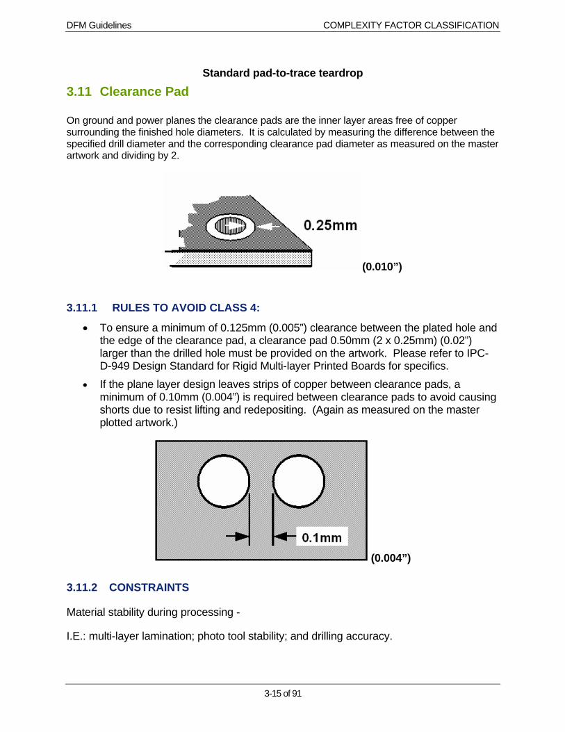
On ground and power planes the clearance pads are the inner layer areas free of copper surrounding the finished hole diameters. It is calculated by measuring the difference between the specified drill diameter and the corresponding clearance pad diameter as measured on the master artwork and dividing by 2.
(0.010”)
3.11.1 RULES TO AVOID CLASS 4:
• To ensure a minimum of 0.125mm (0.005”) clearance between the plated hole and the edge of the clearance pad, a clearance pad 0.50mm (2 x 0.25mm) (0.02”) larger than the drilled hole must be provided on the artwork. Please refer to IPC-D-949 Design Standard for Rigid Multi-layer Printed Boards for specifics.
• If the plane layer design leaves strips of copper between clearance pads, a minimum of 0.10mm (0.004”) is required between clearance pads to avoid causing shorts due to resist lifting and redepositing. (Again as measured on the master plotted artwork.)
(0.004”)
3.11.2 CONSTRAINTS
Material stability during processing -
I.E.: multi-layer lamination; photo tool stability; and drilling accuracy.
DFM Guidelines COMPLEXITY FACTOR CLASSIFICATION
3-16 of 91
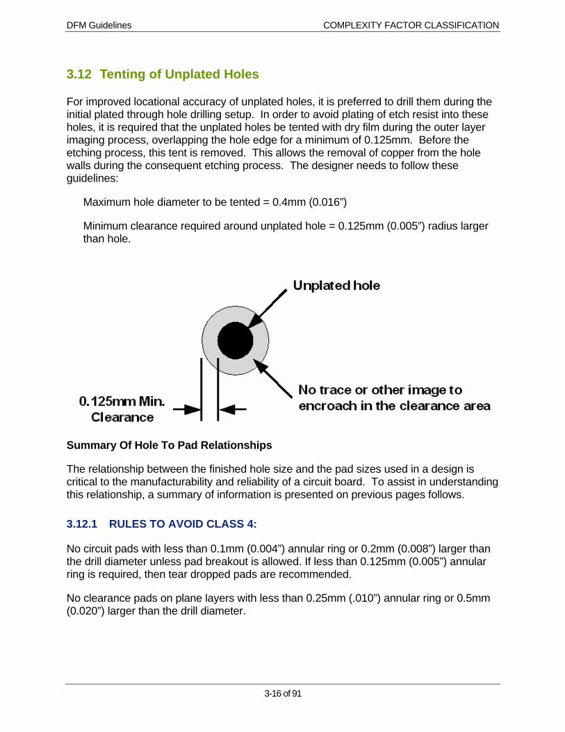
3.12 Tenting of Unplated Holes
For improved locational accuracy of unplated holes, it is preferred to drill them during the initial plated through hole drilling setup. In order to avoid plating of etch resist into these holes, it is required that the unplated holes be tented with dry film during the outer layer imaging process, overlapping the hole edge for a minimum of 0.125mm. Before the etching process, this tent is removed. This allows the removal of copper from the hole walls during the consequent etching process. The designer needs to follow these guidelines:
Maximum hole diameter to be tented = 0.4mm (0.016”)
Minimum clearance required around unplated hole = 0.125mm (0.005”) radius larger than hole.
Summary Of Hole To Pad Relationships
The relationship between the finished hole size and the pad sizes used in a design is critical to the manufacturability and reliability of a circuit board. To assist in understanding this relationship, a summary of information is presented on previous pages follows.
3.12.1 RULES TO AVOID CLASS 4:
No circuit pads with less than 0.1mm (0.004”) annular ring or 0.2mm (0.008”) larger than the drill diameter unless pad breakout is allowed. If less than 0.125mm (0.005”) annular ring is required, then tear dropped pads are recommended.
No clearance pads on plane layers with less than 0.25mm (.010”) annular ring or 0.5mm (0.020”) larger than the drill diameter.
DFM Guidelines COMPLEXITY FACTOR CLASSIFICATION
3-17 of 91
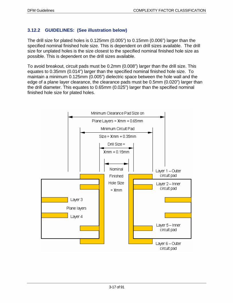
3.12.2 GUIDELINES: (See illustration below)
The drill size for plated holes is 0.125mm (0.005”) to 0.15mm (0.006”) larger than the specified nominal finished hole size. This is dependent on drill sizes available. The drill size for unplated holes is the size closest to the specified nominal finished hole size as possible. This is dependent on the drill sizes available.
To avoid breakout, circuit pads must be 0.2mm (0.008”) larger than the drill size. This equates to 0.35mm (0.014”) larger than the specified nominal finished hole size. To maintain a minimum 0.125mm (0.005”) dielectric space between the hole wall and the edge of a plane layer clearance, the clearance pads must be 0.5mm (0.020”) larger than the drill diameter. This equates to 0.65mm (0.025”) larger than the specified nominal finished hole size for plated holes.

DFM Guidelines COMPLEXITY FACTOR CLASSIFICATION
3-18 of 91
3.13 Finished Board Thickness
The maximum finished board thickness measured copper to copper. This measurement is critical to the fabricator as it affects aspect ratio, drilling and profiling stack heights, and fixed limitations of processing equipment. For additional information please refer to the Materials Section.
3.13.1 GUIDELINES:
• The overall board thickness including solder mask must be between 0.5mm (0.020”) and 6.85mm (0.270”).
3.13.2 CONSTRAINTS
Plating racks, Electroless baskets, U.L. Flammability rating, Outer Layers scrubbers, laminators. Boards less than 1.3mm (0.050”) require special handling and processing at the Hot-Air-Leveling operation, which negatively affects machine capacity and affects cost.
3.13.3 ASPECT RATIO
The maximum board thickness divided by the smallest selected drill diameter. The maximum board thickness is the calculated thickness over copper before plating. Additional thickness caused by plating, hot air solder leveling, or solder mask has no impact on aspect ratio.
Y
z

DFM Guidelines COMPLEXITY FACTOR CLASSIFICATION
3-19 of 91
3.14 Aspect Ratio Plating Capability
Drilled Board Thickness (mm)/Aspect Ratio
Hole Size mm (inch)
1.8 (0.070”)
2.35 (0.093”)
3.15 (0.125”)
6.75 (0.266”)
1.65 (0.065”) OK OK OK 4.1 : 1
1.15 (0.045”) OK OK OK 5.9 : 1
0.9 (0.035”) OK OK OK 7.6 : 1
0.65 (0.025”) 2.8 : 1 3.7 : 1 5.0 : 1 10.6 : 1
0.5 (0.020”) 3.5 : 1 4.65 : 1 6.25 : 1 13.3 : 1
0.45 (0.018”) 3.9 : 1 5.1 : 1 6.9 : 1 14.7 : 1
0.4 (0.016”) 4.4 : 1 5.8 : 1 7.8 : 1
0.35 (0.014”) 5.2 : 1 6.8 : 1 9.3 : 1
0.3 (0.012”) 5.6 : 1 7.4 : 1
0.25 (0.010”) 7 : 1 9.3 : 1
Note: This Aspect Ratio Matrix provides general guidelines for establishing aspect ratio capability. If board thickness and minimum drill size vary considerably from above data, please contact the PCB manufacturer.
DFM Guidelines COMPLEXITY FACTOR CLASSIFICATION
3-20 of 91
3.15 Overall Finished Profile Tolerance
The finished board profile dimensions and tolerances as specified on the drawing.
3.15.1 RULES TO AVOID CLASS 4:
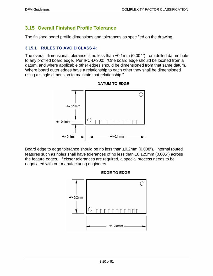
The overall dimensional tolerance is no less than ±0.1mm (0.004”) from drilled datum hole to any profiled board edge. Per IPC-D-300: "One board edge should be located from a datum, and where applicable other edges should be dimensioned from that same datum. Where board outer edges have a relationship to each other they shall be dimensioned using a single dimension to maintain that relationship."
DATUM TO EDGE
Board edge to edge tolerance should be no less than ±0.2mm (0.008”). Internal routed features such as holes shall have tolerances of no less than ±0.125mm (0.005”) across the feature edges. If closer tolerances are required, a special process needs to be negotiated with our manufacturing engineers.
EDGE TO EDGE

DFM Guidelines COMPLEXITY FACTOR CLASSIFICATION
3-21 of 91
3.15.2 X/Y AXIS PROFILING
Use the most generous tolerance that the product will allow to minimize board price. Additionally, use only one cutter size. The preferred cutter size for routing is 3.175mm (0.125 inch) or 2.36mm (0.093 inch) diameter. Avoid use of smaller cutters.
Avoid routing through metal features. The result requires excessive hand de-burring and can cause quality defects.
3.15.3 SPECIAL TIGHT TOLERANCE PROFILE PROCESS:
Double routing of internal features (holes or cutouts) can be applied in any axis. Tolerance shall be no less than ±0.1mm (0.004”) across routed edges of the feature.
Double routing of external features can be performed in one axis of the circuit board only due to material and tooling stability. Tolerance shall be no less than ±0.125mm (0.005”) from feature edge to feature edge in the double rout axis. The opposite axis defaults to ±0.2mm (0.008”) tolerance.
EDGE TO EDGE
(Double Route)
3.15.4 CONSTRAINTS The standard cutter sizes produce the following radii 1.57mm (0.062”), 1.194mm (0.047”), and 0.787mm (0.031”) = 1.57mm (0.062”) cutter. Conventional pin routing requires a minimum of two pins per board. Pin sizes to be greater than 1.57mm (0.062”) and less than 6.375mm (0.251”).

DFM Guidelines COMPLEXITY FACTOR CLASSIFICATION
3-22 of 91
3.16 Tab Routing
The preference is to set up parts for tab routing as a function of the tooling operation. To avoid unnecessary modifications to the mechanical drawing, it is preferred that customer provide only a note stating that the part needs to be shipped in panel form, delta notes indicating where tabs cannot be located. If the location of the parts in the panel is critical, the dimensions of the datums of the parts to the component assembly locating holes must be provided.
The following are the parameters used in setting up a tab routed panelized part:
• Locate tabs 9mm (0.35”) minimum from any board corners.
• Place tabs 9mm (0.35”) minimum from any board corners.
• Place tabs 9mm (0.35”) minimum from datum holes, or directly on center.
• A 3.175mm (0.125”) cutter will be utilized, unless design requires otherwise. All cut paths that are not between boards will be 3.175mm (0.125’) wide; preferred spacing between boards is 6.35mm (0.25”), 3.8mm (0.15”) minimum.
• Place tabs 75mm ±12mm (3.00” ±0.50”) apart from each other.
• Keep tabs in a straight line with X - Y axis if possible.
• Where there are component holes or traces close to the board edge, try to avoid tabbing in these areas to prevent the traces or hole walls from fracturing.
• Tab width is 3mm ±0.25mm (0.118” ±0.010”).
• Tab location dimension is ±0.5mm (±0.020”).
• Dimension tabs to the center of the tab on a 0.5mm (0.020”) grid.
• Place tabs ±6mm (±0.236”) minimum away from any radius on the outside board edge.
KEY REQUIREMENTS
Specification Preferred Available / Special Options:
Routing:
Edge-to-edge tolerance: +/- 0.25mm (0.010”) +/- 0.2mm (0.008”)
Edge-to-datum hole tolerance: +/- 0.125mm (0.005”) +/- 0.09mm (0.0035”)
Minimum internal radius: 0.8mm (0.031”) 0.4mm (0.0155”)
Minimum external radius: None None
Max. routed hole diameter and tol: 31.75mm (1.250” ±0.010”) 31.75mm (1.250” ±0.005”)
Min. routed hole diameter and tol: 6.35mm (0.250” ±0.005”) 6.35mm (0.250” ±0.003”)
Preferred router bits: 2.375mm (0.0935”) 1/32”, 1/8”, 0.040”, 0.050”
DFM Guidelines COMPLEXITY FACTOR CLASSIFICATION
3-23 of 91
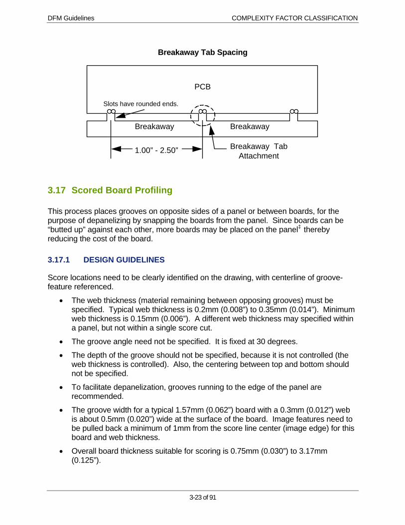
Breakaway Tab Spacing
1.00” - 2.50”
Breakaway Breakaway
PCB
Breakaway TabAttachment
Slots have rounded ends.
3.17 Scored Board Profiling
This process places grooves on opposite sides of a panel or between boards, for the purpose of depanelizing by snapping the boards from the panel. Since boards can be “butted up” against each other, more boards may be placed on the panel‡ thereby reducing the cost of the board.
3.17.1 DESIGN GUIDELINES
Score locations need to be clearly identified on the drawing, with centerline of groove-feature referenced.
• The web thickness (material remaining between opposing grooves) must be specified. Typical web thickness is 0.2mm (0.008”) to 0.35mm (0.014”). Minimum web thickness is 0.15mm (0.006”). A different web thickness may specified within a panel, but not within a single score cut.
• The groove angle need not be specified. It is fixed at 30 degrees.
• The depth of the groove should not be specified, because it is not controlled (the web thickness is controlled). Also, the centering between top and bottom should not be specified.
• To facilitate depanelization, grooves running to the edge of the panel are recommended.
• The groove width for a typical 1.57mm (0.062”) board with a 0.3mm (0.012”) web is about 0.5mm (0.020”) wide at the surface of the board. Image features need to be pulled back a minimum of 1mm from the score line center (image edge) for this board and web thickness.
• Overall board thickness suitable for scoring is 0.75mm (0.030”) to 3.17mm (0.125”).

DFM Guidelines COMPLEXITY FACTOR CLASSIFICATION
3-24 of 91
KEY REQUIREMENTS
Specification Preferred Available / Special Options:
Scoring:
Minimum web thickness: 0.1mm (0.004”)
Available scoring angles: 30° 20°, 45°, 60°
Spacing between V-sore to copper 0.635mm (0.025”) 0.50mm (0.020”)
Web thickness tolerance: 0.125mm (±0.005”) 0.075mm (0.003”)
Location tolerance: 0.125mm (±0.005”)
Jump score capability: Yes
Saw Slot Diagrams Achievable Tolerances:
Web Thickness..............................±0.05mm (0.002”)
Edge to Edge.................................±0.125mm (0.005”)
Datum to Edge ..............................±0.2mm (0.008”)
3.17.2 CONSTRAINTS
• Diagonal scores or curved scores are not possible. Scores must be parallel to edge of panel.
• The circular 100mm (4.00”) diameter saw blade causes an over-run at the ends of each cut. For a typical 1.57mm (0.062”) board with a 0.3mm (0.012”) web, this over-run amounts to approximately 7.5mm (0.30”). The distance between boards on a panel must compensate for this, if the boards are offset on the panel.
• Because of problems associated with stacked tolerances in conjunction with multiple set-ups, it is not recommended to have both scoring and profile routing on the same panel.
• With the exception of panel borders, scoring should not cut metal.

DFM Guidelines COMPLEXITY FACTOR CLASSIFICATION
3-25 of 91
3.18 Hand Finishing Operations
3.18.1 MANUAL EDGE MILL
Boards may require edge milling to reduce the circuit board thickness to a specified thickness and tolerance. Typically this is done to allow the board to fit into a card guide when assembled.
The milled edge is usually a "step" at the edge of the board. See diagram below. The depth of the step is variable from 0.25mm (0.635”) removed to 0.8mm (0.032”) remaining. The width of the step is variable from 0.5mm (0.020”) to 9.5mm (0.38”). Milling requirements should be limited to simple cuts i.e. two straight edges and simple corners. The path of the mill is limited to 90° turns and internal radii are controlled by cutter diameter. Minimum 3.2mm (0.125”) and common standard sizes. Geometries other than a step are possible but need to be evaluated on an individual basis as processing time is prohibitive. Double sided milling is strongly discouraged as edge thickness accuracy is reduced.
The finished thickness of the milled edge can be held to ±0.2mm (0.008”) inch for a single sided milled edge. For a double sided milled edge the finished thickness can be held to ±0.25mm (±0.010”). The width of the step can be held to ±0.25mm (±0.010”).
Internal tooling pins are required. These tooling holes must be internal to the finished board and should be located as close as possible (but not actually in) the portion of the board to be milled. The finish produced by the mill process is similar to that produced by NC edge profiling. No fractured glass fibers are produced.
DFM Guidelines COMPLEXITY FACTOR CLASSIFICATION
3-26 of 91
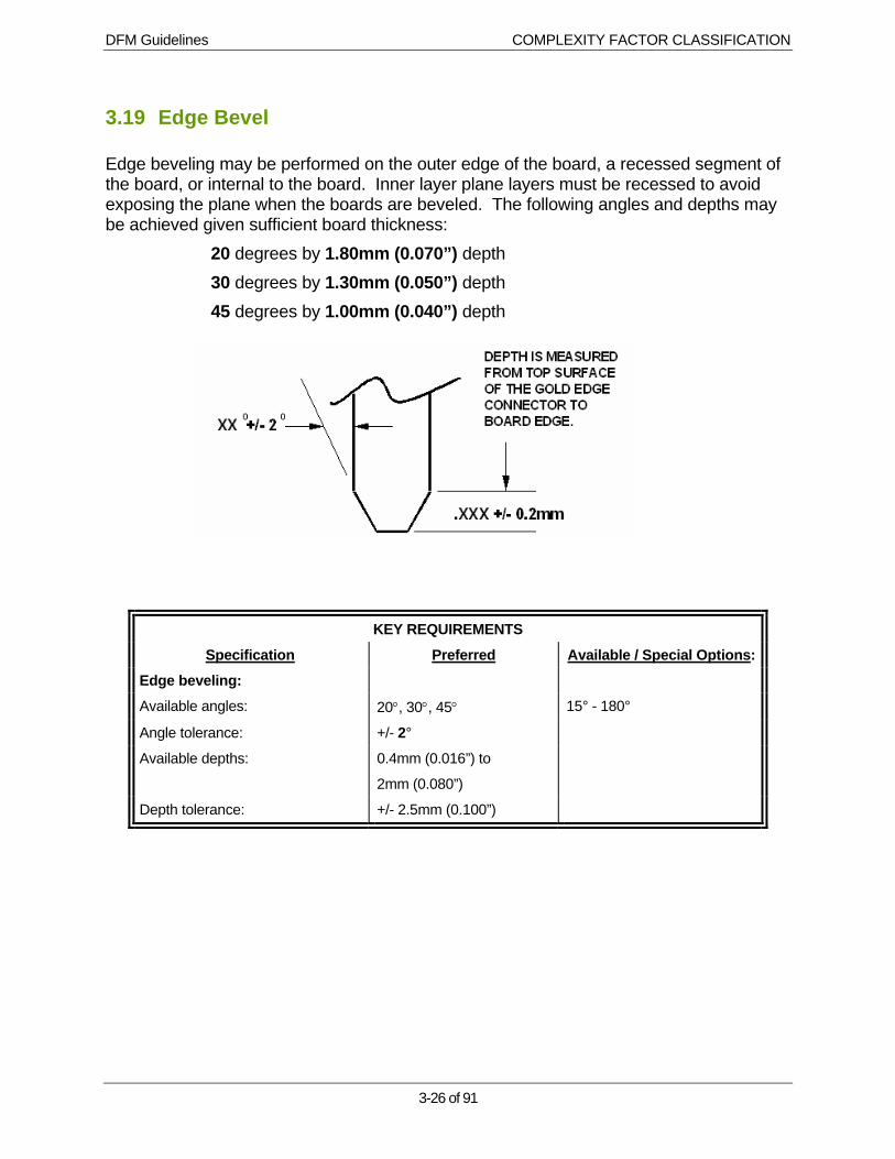
3.19 Edge Bevel
Edge beveling may be performed on the outer edge of the board, a recessed segment of the board, or internal to the board. Inner layer plane layers must be recessed to avoid exposing the plane when the boards are beveled. The following angles and depths may be achieved given sufficient board thickness: 20 degrees by 1.80mm (0.070”) depth 30 degrees by 1.30mm (0.050”) depth 45 degrees by 1.00mm (0.040”) depth
KEY REQUIREMENTS
Specification Preferred Available / Special Options:
Edge beveling:
Available angles: 20°, 30°, 45° 15° - 180°
Angle tolerance: +/- 2°
Available depths: 0.4mm (0.016”) to
2mm (0.080”)
Depth tolerance: +/- 2.5mm (0.100”)
DFM Guidelines PLATING OPTIONS
4-1 of 91
4 PLATING OPTIONS For plated-through-hole circuit boards, electroless copper, followed by electro-plated copper is deposited onto the hole wall to an average thickness of 0.025mm (0.001”). During the copper electro-plating process, external lines receive an average of .025mm (0.001”) copper plating, in addition to the original 0.5 or 1 oz copper foil already present.
All exposed circuitry, depending on specifications either before or after solder mask, needs to be protected by one of the finishes identified below.
Immersion Silver
• Typical coating thickness: 0.20 µm (0.00007”) to 0.50 µm (0.0002”) • Excellent solderability • Excellent surface coplanarity and hole size uniformity • Excellent for use in fine pitch component technology • Improved surface contrast - assembly vision capability • Board not subjected to thermal shock (as with HASL) • Best for “Lead Free” soldering
Nickel - Hard Gold • Typical thickness: 0.7 µm (0.00003”) to 1.3 µm (0.00005”) gold (99.7%) over 5.0
µm (0.0002”) nickel or 0.2 µm (0.000008”) to 0.3 µm (0.00001”) gold (99.7%) over 5.0 µm (0.0002”) nickel for a solderable surface
• Excellent corrosion resistance • 130 to 220 Knoop hardness • Excellent wear resistance, best for surface rotary switches, on-off contacts, and
edge connectors • Excellent shelf life
Nickel - Soft Gold • Typical thickness: 0.7 µm (0.00003”) to 1.3 µm (0.00005”) gold (99.9%) over 5.0
µm (0.0002”) nickel • Excellent corrosion resistance • Less than 90 Knoop hardness • Good for pressure contacts and aluminum or gold-wire bonding • Fair wear resistance • Excellent shelf life

DFM Guidelines PLATING OPTIONS
4-2 of 91
Electroless Nickel/Immersion Gold (99.9% Gold)
• Typical thickness: 0.08 µm (0.000003”) to 0.2 µm (0.000008”) gold over 0.5 µm (0.0002”) nickel
• Excellent corrosion resistance
• Good for aluminum wire bonding
• Excellent for fine-pitch technology
• Excellent solderability
• Excellent shelf life
HASL (Eutectic: 63% Tin - 37% Lead)
• Typical coating thickness: 0.8 µm (0.000003”) to 5 µm (0.0002”), design dependent.
• Excellent solderability
• 0.635mm (0.025”) SMT pitch or higher capability
• 0.75mm (0.030”) minimum board thickness capability
• Good shelf life
Organic Solderability Preservative (OSP) or Anti-tarnish‡
• Typical coating thickness: 0.2 µm (0.000008”) to 0.5 µm (0.0002”) • Excellent solderability
• Excellent surface coplanarity and hole size uniformity
• Excellent for use in fine-pitch technology
• Improved surface contrast - assembly vision capability
• Board not subjected to thermal shock (as with HASL)
• Good shelf life (12 months)
Nickel - Matte Tin
• Typical thickness: 7.6 µm (0.0003”) Tin over 12.7 (0.0005”) µm nickel • Solderable surface
• Good shelf life

DFM Guidelines PLATING OPTIONS
4-3 of 91
4.1 Gold Plating
4.1.1 OBJECTIVE
To communicate rules and guidelines for the design of gold contact areas on high density printed circuit boards. By understanding the processing constraints of the double image processes the circuit board designer can have a positive influence on the board price.
4.2 Selective or Double Image Plating
This process is reserved for parts that have requirements for gold areas internal to the board. It requires the extra labor and materials associated with double image plating.
4.2.1 DESIGN CONSTRAINTS
The tin image should include all the plated area excluding that called out to be gold plated (tin plating should not overlap into the gold plated area). The gold image should include all of the area designated to be gold plated on the drawing.
The gold image overlap into the tin area is between 1.25mm (0.050”) to 2.5mm (0.100”).
In the double image area, holes must be supported with pads on both sides having the same type of plating, either tin or gold. If it is necessary to plate both gold and tin in the same hole, then a breakout pad must be provided within the tin film on the opposite side of the standard pad. If a hole is required to be gold plated, then the minimum copper thickness requirement in this hole must be waived.
Internal finger contacts, when called out to be gold plated, should include the entire contact area.
The trace width in the overlap area must be 0.25mm (0.100”) minimum.
The spacing between parallel runs or pads within the overlap area should be greater than 0.4mm (0.016”). If the spacing is less than 0.4mm (0.016”), then the overlap must be staggered by 0.5mm (0.020”) minimum.
DFM Guidelines PLATING OPTIONS
4-4 of 91
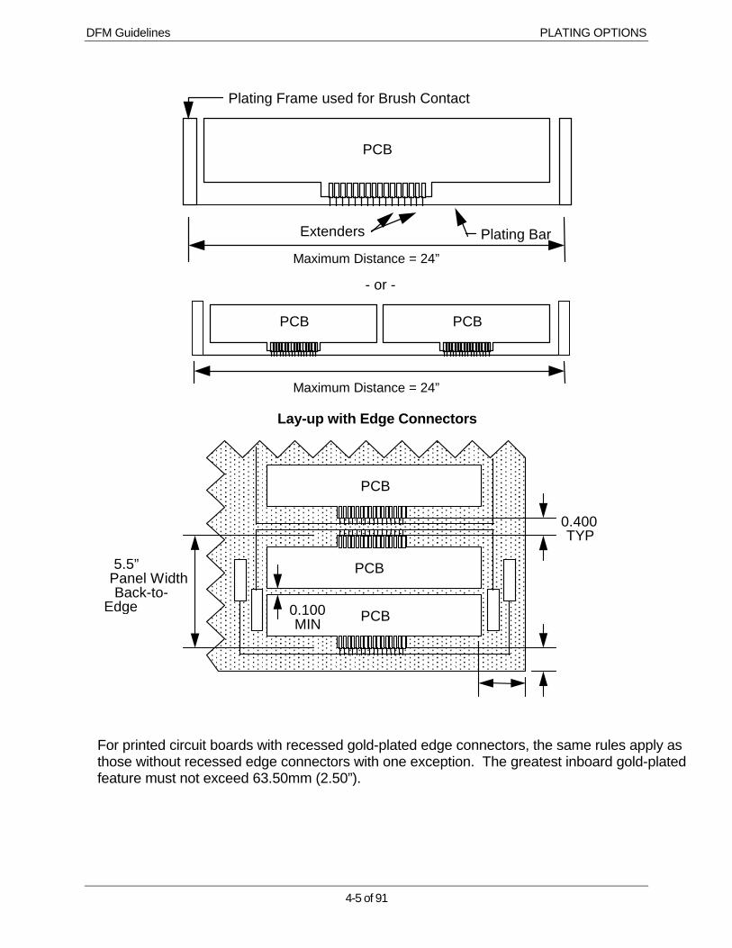
4.3 Edge Connector Plating
The preferred manufacturing process for gold plating of edge connectors is tab plating. This process does not require the extra labor and materials associated with double image plating.
4.3.1 DESIGN CONSTRAINTS
• The maximum length of the gold plated tab is plated 20mm (0.80”).
• The maximum plating depth is 63.5mm (2.50”) from the shear line (see diagram on next page).
• A minimum distance of 0.75mm (0.030”) between contact pads allows good plating tape adherence and a well defined line between the gold plated area and the solder coated area.
• The annular ring of a through hole must be a minimum of 0.75mm (0.030”) from the edge of the gold plated area to prevent “black holes”, resulting in solderability problems. It is best to keep holes as far away as possible from the gold edge connector area.
Note: The tab plate process is not set up for through hole plating. It is a surface plating process. Gold over nickel plating of the hole wall would be unreliable.
• Maximum distance between buss bar connections: 610mm (24.00”)
• Minimum PCB thickness: 0.8mm (0.032”)
• Maximum PCB thickness: 3.2mm (0.125”)
• Maximum edge connector recess: 63.5mm (2.50”) (min. allowable solution level)
DFM Guidelines PLATING OPTIONS
4-5 of 91
Extenders Plating Bar
Plating Frame used for Brush Contact
Maximum Distance = 24”
- or -
PCB
PCB PCB
Maximum Distance = 24”
Lay-up with Edge Connectors
PCB
PCB
PCB
0.400TYP
0.100MIN
5.5” Panel Width Back-to-
Edge
For printed circuit boards with recessed gold-plated edge connectors, the same rules apply as those without recessed edge connectors with one exception. The greatest inboard gold-plated feature must not exceed 63.50mm (2.50”).
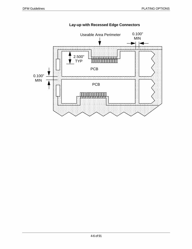
DFM Guidelines PLATING OPTIONS
4-6 of 91
Lay-up with Recessed Edge Connectors
PCB
0.100” MIN
2.500”TYP
Useable Area Perimeter
0.100” MIN
PCB

DFM Guidelines SOLDER MASK
5-1 of 91
5 SOLDER MASK
5.1 Objective
To communicate rules and guidelines for designing solder mask artwork based on mask type.
Solder Mask Availability
A variety of solder Masks have been selected to fill the needs of our customers. The following is a description of the solder Masks currently available. The need for closer tolerances has driven the implementation of photo-imageable solder masks.
Liquid Photo-Imageable (LPISM) Solder Masks
Enthone DSR 3241 ‡ is applied using the flood screen coating process, while PROBIMER 52M® is applied via the curtain coating process. Enthone DSR 3241 has a green semi matte finish. Enthone DSR 3241 solder mask has improved resolution capability, meaning that it can hold a finer feature, such as a “dam” between SMT pads. Liquid Photo-imageable solder masks are considered to be solder masks of choice for most circuit board product due to their high resolution, excellent electrical properties and compatibility with surface mount technology.
Hole “tenting” is available through the via-cap process in which PC401®, a thermally cured epoxy, is screened over the holes to be tented, after liquid photo-imageable solder Mask is applied. This is an advantage for vacuum applications after assembly.
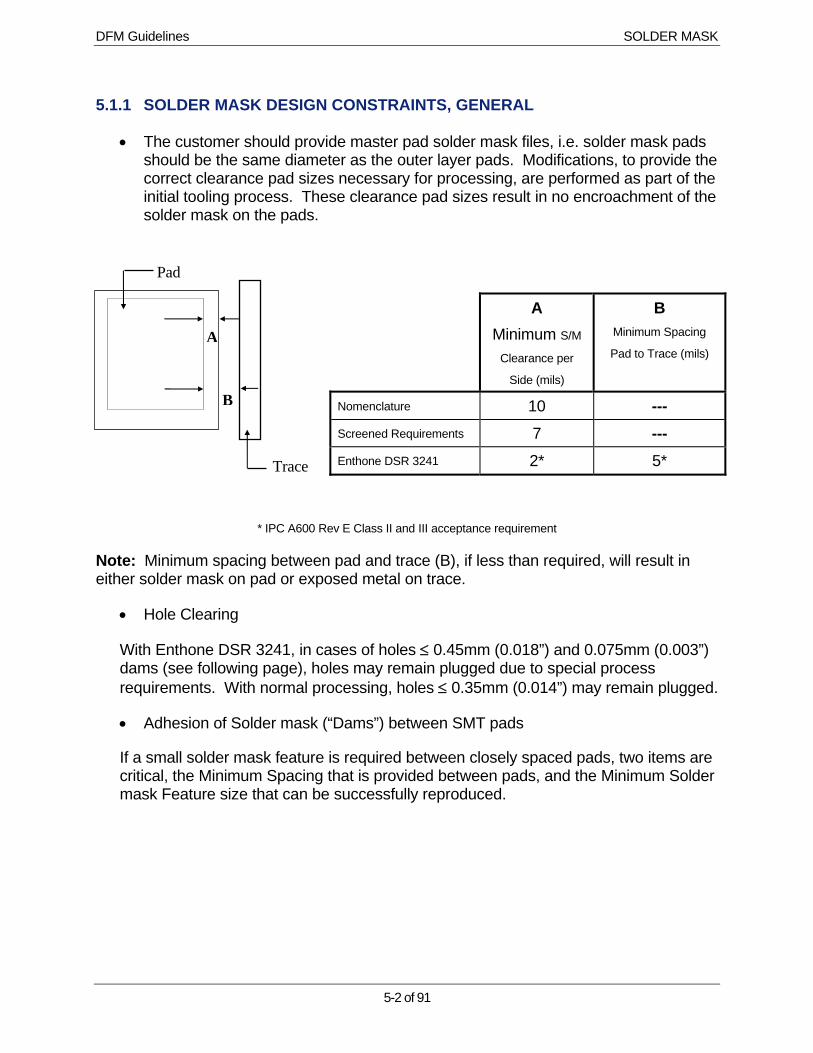
DFM Guidelines SOLDER MASK
5-2 of 91
5.1.1 SOLDER MASK DESIGN CONSTRAINTS, GENERAL
• The customer should provide master pad solder mask files, i.e. solder mask pads should be the same diameter as the outer layer pads. Modifications, to provide the correct clearance pad sizes necessary for processing, are performed as part of the initial tooling process. These clearance pad sizes result in no encroachment of the solder mask on the pads.
A
Minimum S/M
Clearance per
Side (mils)
B Minimum Spacing
Pad to Trace (mils)
Nomenclature 10 --- Screened Requirements 7 --- Enthone DSR 3241 2* 5*
* IPC A600 Rev E Class II and III acceptance requirement
Note: Minimum spacing between pad and trace (B), if less than required, will result in either solder mask on pad or exposed metal on trace.
• Hole Clearing
With Enthone DSR 3241, in cases of holes ≤ 0.45mm (0.018”) and 0.075mm (0.003”) dams (see following page), holes may remain plugged due to special process requirements. With normal processing, holes ≤ 0.35mm (0.014”) may remain plugged.
• Adhesion of Solder mask (“Dams”) between SMT pads
If a small solder mask feature is required between closely spaced pads, two items are critical, the Minimum Spacing that is provided between pads, and the Minimum Solder mask Feature size that can be successfully reproduced.
Trace
Pad
A
B

DFM Guidelines SOLDER MASK
5-3 of 91
To assure no solder mask on any pad in an SMD array, the minimum solder mask clearance for a surface mount pad is 0.05mm (0.002”) per side (not applicable for panel sizes over 18” x 24”). As space permits, a clearance of 0.06mm (0.0025”) per side is preferred.
Clear Soldermask( Individual Webs )
Green Soldermask( Individual Webs )
0.0035” S/M Web
0.0025” Clearance
0.003” S/M Web
0.0025”Clearance
Fine PitchSMD Pads
0.002”Clearance
Gang Relief ( Clear or Green Soldermask )
Note: If pads are closer than the minimum spacing described above, areas between pads should be free of solder mask, or the hold-down reliability will not be 100%.
The strength of solder mask adhesion over gold plating depends on the type of solder mask, type of gold, and the end-user processing conditions. It is recommended that the designer contact the PCB manufacturer before finalizing design.
• When using clear solder mask, mask features below 0.075mm (0.003”) are not allowed (as measured on the CAD data). Similarly, mask features below 0.09mm (0.0035”) are not allowed for green solder mask.
• Allow 0.75mm (0.030”) per-side solder mask clearance for score lines.
• To prevent solder mask from going into and/or plugging a hole, solder mask clearance should be 0.010” (0.005” per side) larger than the pad size on both sides of the board.
• The primary coating of LPI solder mask shall not be used to tent holes.

DFM Guidelines SOLDER MASK
5-4 of 91
5.2 Tenting of Via Holes with Solder Mask
5.2.1 VIA CAPPING WITH SCREENED RESIST
Hole capping is available through the Via Cap process. On boards coated with liquid photo-imageable mask, the vias can be screened with solder mask creating an epoxy cap. Artwork modifications necessary for processing are performed as part of the initial tooling. A separate design file must be provided by the customer, which includes only those vias which are to be capped. The customer needs to provide master pad solder mask and via files, i.e. solder mask and via pads that are the same size as the outer layer pads.
5.2.2 VIA CAPPING DESIGN CONSTRAINTS
• The maximum finished hole size for via capping is 0.50mm (0.020”) diameter. Preferred drill diameter 0.53mm (0.021”).
• Generally, the non-test vias are capped on the Top Side of the board, especially under BGA components. Via capping on both sides results in raised or broken caps. Therefore, it should be avoided.
• Via caps will have a raised surface of about 0.06mm ±0.05mm (0.0025” ±0.002”) above the outer layer copper pad. This measurement may include solder and/or permanent solder mask thickness.
• The PCB manufacturer will guarantee a minimum of 98% of holes plugged, with open holes randomly located.

DFM Guidelines SOLDER MASK
5-5 of 91
5.3 Peelable Solder Mask
Peelable solder mask (PSM) is a temporary solder mask which is selectively applied to a circuit board prior to the Hot Air Solder Leveling (HASL) process. Its purpose is to protect gold plated surfaces from being coated with solder. After the HASL process, the PSM is removed manually.
A 0.030
B 0.036
A = Minimum distance between a gold contact and a gold feature or unplated hole.B = Minimum distance between gold contact and a connected copper feature
Peelable Soldermask design requirement
Peelable soldermask
5.3.1 PEELABLE SOLDER MASK CONSTRAINTS
• If PSM terminates in the bare glass areas around pads (or other areas not covered with permanent mask), it will leave a blue residue in those areas.
• A maximum of 24 individual strips of PSM is allowed per panel. This is to minimize the time required to manually peel PSM strips from panel.
• The permanent solder mask file must provide a minimum coverage of the copper/gold interface (see drawing).
It is recommended that the designer discuss PSM requirements with Wind River Systems before finalizing design.
5.3.2 NOMENCLATURE
• Letter size: ≥ 0.15mm (0.006”) Line Width, ≥ 1.0mm (0.040”) Height.
• Color: White preferred; Yellow, Orange and Black also available.
• Nomenclature over Solder (HASL) will have poor adherence.
• Nomenclature placed over bare copper before HASL will have an apparent copper “halo” after the HASL

DFM Guidelines BLIND AND BURIED VIA (BBV) BOARDS
6-1 of 91
6 BLIND AND BURIED VIA (BBV) BOARDS
6.1 General description
Like through holes in a conventional multi-layer board, blind and/or buried vias are holes that make connections between layers. However, unlike in a conventional multi-layer board, blind and buried vias allow circuits of non-planar topography to be connected. This is important, as it conserves circuit board real-estate because it allows only necessary layers to be connected.
Wind River Systems uses the following terminology to define different types of drilled interconnection:
• A through hole via has access to both external layers.
• A blind via does not pass through the entire board, and has access to only one external layer.
• A buried via provides connection within inner layers, it has no access to the external layers.
Through Hole ViaBuried Via
Blind Vias
Example of 6 Layer BBV Board

DFM Guidelines BLIND AND BURIED VIA (BBV) BOARDS
6-2 of 91
6.1.1 Blind & Buried Via Design Constraints
• U.L. limitation of a maximum of three thermal press cycles. The above example requires two such cycles: First, to laminate layers 1/2 to 3/4; second, to laminate layers 1/2 and 3/4 to 5/6.
• Core thickness 0.075mm (0.003”) minimum.
Note: 0.5 ounce copper is required for BBV layers. Individual BBV layers will receive 18µm (0.0007”) electrolytic copper during the through-hole plating process, bringing the total copper thickness to 35µm (0.0014”).
• Minimum drill size 0.2mm (0.008”) with a maximum aspect ratio of 7:1 for blind/buried via substrates.
Note: All BBV holes will be plugged with epoxy during subsequent lamination cycles.
• The ability to register drilled holes to inner layers is impacted after each lamination cycle.
Minimum Annular Ring: Drilled before first press cycle - 0.1mm per side
Drilled after first press cycle - 0.1mm (0.004”) per side
Drilled after second press cycle - 0.15mm (0.006”) per side
Drilled after third press cycle - 0.23mm (0.009”) per side
• Multi-layer design recommendations as outlined in section 2.9 apply.
Required information on drawings:
• The hole chart must list plated through holes separately from the BBV holes.

DFM Guidelines CONTROLLED IMPEDANCE
7-1 of 91
7 CONTROLLED IMPEDANCE
7.1 Characteristic Impedance
The characteristic impedance of a transmission line is dependent on the relationship of the conductor width, conductor thickness, dielectric thickness between conductor and ground-power reference planes, and the dielectric constant of the dielectric medium.
It is recommended that the designer contact Wind River Systems to discuss impedance needs during the initial design phase. This will enable mutual understanding of requirements and impact of material characteristics, such as specific Dk’s and manufacturing processes, on needed impedance targets and tolerances.
The actual impedance may have to be tested via a small prototype build. This is often necessary when tight impedance tolerances are required, or in the case of small line widths and dielectric thicknesses, which are more sensitive to variations. A tolerance swing due to etching variations will be more significant for a 0.125mm (0.005”) line width than for a 0.25mm (0.100”) line, for example.
Line width and dielectric thicknesses should be documented as reference dimensions only. This will allow Wind River Systems to make small adjustments to both parameters in order to match impedance targets.
Note: If a line width modification is necessary, it will only be accomplished globally. That is, all of the lines of the same width will be modified on a given layer. No modification will be made without prior consent of the customer.
For impedance calculations, it is important to consider the Etch Factor, the effective reduction of the line width during the etching process. (See section 3.3). The exception to this is with boards with an Aspect Ratio GE 4.5:1 or with boards GE 2.3mm (0.093”) thick and an Aspect Ratio of GE 3:1. No Etch Factor needs to be considered in these cases.
The recommended impedance tolerance is ±10%. A lesser tolerance is often achievable, especially with fully embedded Microstrip and Stripline structures. This requirement must be discussed with Wind River Systems for appropriate focus.
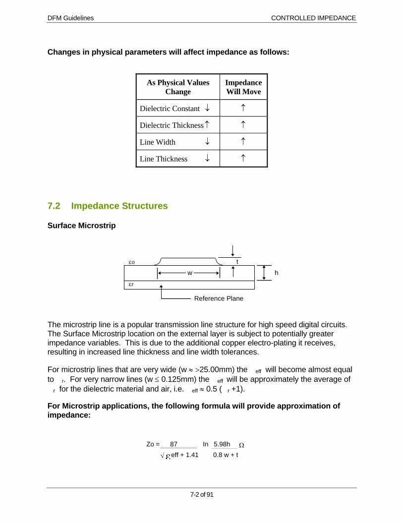
DFM Guidelines CONTROLLED IMPEDANCE
7-2 of 91
Changes in physical parameters will affect impedance as follows:
As Physical Values Change
Impedance Will Move
Dielectric Constant ↓ ↑
Dielectric Thickness ↑ ↑
Line Width ↓ ↑
Line Thickness ↓ ↑
7.2 Impedance Structures
Surface Microstrip
t
h
Reference Plane
w
εo
εr
The microstrip line is a popular transmission line structure for high speed digital circuits. The Surface Microstrip location on the external layer is subject to potentially greater impedance variables. This is due to the additional copper electro-plating it receives, resulting in increased line thickness and line width tolerances.
For microstrip lines that are very wide (w ≈ >25.00mm) the eff will become almost equal to r. For very narrow lines (w ≤ 0.125mm) the eff will be approximately the average of r for the dielectric material and air, i.e. eff ≈ 0.5 (r +1).
For Microstrip applications, the following formula will provide approximation of impedance:
Zo = 87 In 5.98h Ω √ εeff + 1.41 0.8 w + t
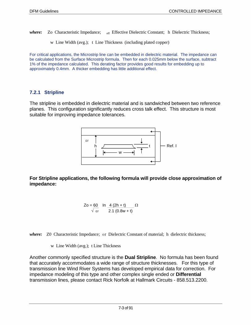
DFM Guidelines CONTROLLED IMPEDANCE
7-3 of 91
where: Zo Characteristic Impedance; eff Effective Dielectric Constant; h Dielectric Thickness;
w Line Width (avg.); t Line Thickness (including plated copper)
For critical applications, the Microstrip line can be embedded in dielectric material. The impedance can be calculated from the Surface Microstrip formula. Then for each 0.025mm below the surface, subtract 1% of the impedance calculated. This derating factor provides good results for embedding up to approximately 0.4mm. A thicker embedding has little additional effect.
7.2.1 Stripline
The stripline is embedded in dielectric material and is sandwiched between two reference planes. This configuration significantly reduces cross talk effect. This structure is most suitable for improving impedance tolerances.
Ref. Pεr
hw
t
For Stripline applications, the following formula will provide close approximation of impedance:
Zo = 60 In 4 (2h + t) Ω√ εr 2.1 (0.8w + t)
where: Z0 Characteristic Impedance; er Dielectric Constant of material; h dielectric thickness;
w Line Width (avg.); t Line Thickness
Another commonly specified structure is the Dual Stripline. No formula has been found that accurately accommodates a wide range of structure thicknesses. For this type of transmission line Wind River Systems has developed empirical data for correction. For impedance modeling of this type and other complex single ended or Differential transmission lines, please contact Rick Norfolk at Hallmark Circuits - 858.513.2200.
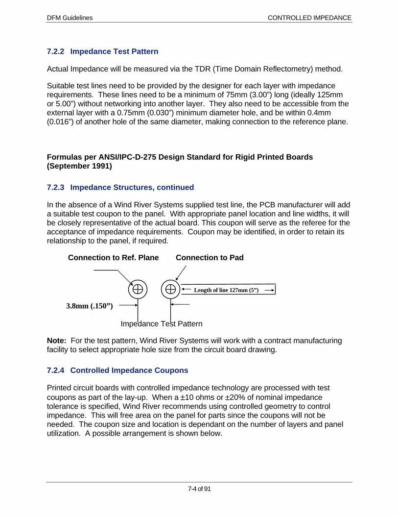
DFM Guidelines CONTROLLED IMPEDANCE
7-4 of 91
7.2.2 Impedance Test Pattern
Actual Impedance will be measured via the TDR (Time Domain Reflectometry) method.
Suitable test lines need to be provided by the designer for each layer with impedance requirements. These lines need to be a minimum of 75mm (3.00”) long (ideally 125mm or 5.00”) without networking into another layer. They also need to be accessible from the external layer with a 0.75mm (0.030”) minimum diameter hole, and be within 0.4mm (0.016”) of another hole of the same diameter, making connection to the reference plane.
Formulas per ANSI/IPC-D-275 Design Standard for Rigid Printed Boards (September 1991)
7.2.3 Impedance Structures, continued
In the absence of a Wind River Systems supplied test line, the PCB manufacturer will add a suitable test coupon to the panel. With appropriate panel location and line widths, it will be closely representative of the actual board. This coupon will serve as the referee for the acceptance of impedance requirements. Coupon may be identified, in order to retain its relationship to the panel, if required.
Connection to Ref. Plane Connection to Pad
Length of line 127mm (5”)
3.8mm (.150”) Impedance Test Pattern
Note: For the test pattern, Wind River Systems will work with a contract manufacturing facility to select appropriate hole size from the circuit board drawing.
7.2.4 Controlled Impedance Coupons
Printed circuit boards with controlled impedance technology are processed with test coupons as part of the lay-up. When a ±10 ohms or ±20% of nominal impedance tolerance is specified, Wind River recommends using controlled geometry to control impedance. This will free area on the panel for parts since the coupons will not be needed. The coupon size and location is dependant on the number of layers and panel utilization. A possible arrangement is shown below.
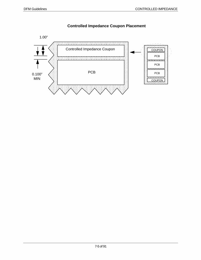
DFM Guidelines CONTROLLED IMPEDANCE
7-5 of 91
Controlled Impedance Coupon Placement
Controlled Impedance Coupon
PCB
1.00”
0.100” MIN
COUPON
COUPON
PCB
PCB
PCB

DFM Guidelines Testing
8-1 of 91
8 Testing
8.1 Testing
Three main test parameters are of interest to customers:
Test Voltage
The amount of power applied to the circuit for testing.
Continuity Resistance
The maximum resistance allowable for a circuit. Any higher resistance indicates a possible open circuit.
Isolation Resistance
The minimum resistance allowable between separate electrical entities. Any lower resistance indicates a possible short.
Testable settings for these parameters are system dependent. The following table identifies the three systems currently available for new designs, the ranges for the parameters on each system, and the maximum testable size for each system.
System Max. Test Voltage
Continuity Resistance
Isolation Resistance
Testable Size
TRACE 948 100v 10 - 600 ohms 1.67 - 100 Megohms 585mm 432mm
TRACE 948 Large Bed
100v 10 - 600 ohms + TSR
600 - 2.5 Megohms 560mm 406mm
TRACE 948 Small Bed
10v 10 - 600 ohms + TSR
600 - 2.5 Megohms 302mm 432mm
ATG TR-1000
10-200v 10 - 100 ohms + TSR
457mm 305mm
TG-4400 10-250v 5 - 1 ohms 100k - 100 Megohms 457mm 610mm
ATG A-1000 10-250v 10-100 ohms 100k - 10 Megohms 406mm 508mm

DFM Guidelines Testing
8-2 of 91
Note: TSR, Test System Resistance, ranges from 2.5 to 6.5 ohms. TSR must be added to stated continuity resistance values to obtain true testable ranges. For example, on TRACE 948, when TSR is 5.03 ohms, true continuity resistance testable range is 8.03 - 605.03 ohms.
Note: It is possible for a test to indicate both open and short between the same test points. When this happens, the board is treated as possibly defective and verified manually.
A Flying test probe is available for PC Boards with less than 72,000 test points total. This is the equivalent of 12 boards with 6000 test points each. One-time builds or once a year builds would be candidates for this fixture-less test. This test is subject to scheduling availability, since each test takes so long.
VOLTAGE RESISTANCE RANGE TESTABLE SIZE
10 - 500v 50 ohms to 100 Megohms 610mm & 685mm
DESIGN REQUIREMENTS FOR CONTINUITY TESTING OF FINE PITCH DEVICES:
To facilitate effective testing of fine pitch SMD devices, down to 0.4mm (0.016”) pitch, a few critical rules must be followed during the design of the board.
Minimum Pitch - The minimum center-to-center distance for SMD pads is currently set at 0.4mm (0.016”).
Minimum Pad Length - (Refer to figure 1.) The minimum pad length for all SMD pads is currently set at 1.5mm.
Grid Location Availability - (Refer to figure 2.) The number of test points, through-holes or SMD pads, in a given area of the board, are limited to the number of test machine grid locations in the same given area. That is, for every test point on a board, there must be a unique test grid location within 2mm (0.008”). When a unique grid location is not available, the test point cannot be tested. This is normally not a problem except when too many SMD pads are located within a very small area.

DFM Guidelines Testing
8-3 of 91
Pin Deflection
Board Test Points
Test MachineGrid Points
Figure 1
Figure 1 illustrates this problem by showing one side of a typical 0.5mm pitch device overlying a 2mm (0.080”) grid of test machine grid locations. For every 2mm (0.080”) down each side of the device, there are five SMD pads, test points. To test all the pads, a swath of five test machine grid locations must be reserved for each side of a 0.5mm pitch quad-pack. Then, pads for two 0.5mm (0.020”) pitch devices can be located no closer than 10mm, with absolutely no other test points, e.g. resistor or capacitor pads, in between. If the quad-packs are closer than 10mm, or if other test points are placed in between, then some test points cannot be tested. Similarly, a swath four locations wide is required for each side of a 0.635mm (0.025”) pitch device. Then, two 0.635mm (0.025”) devices can be located no closer than 8mm (0.32”), with no test points in between.
For 100% testing, there cannot be more test points in a particular area of a board than there are machine grid points in a particular area of a board.
Board-to-Fixture Registration - To facilitate good board-to-fixture registration there should be three unplated holes of sufficient size, 1.8mm (0.032”) to 4mm (0.157”) diameter, positioned such that lines connecting the holes form a triangle. The footprints for all fine pitch devices should fall within or on that triangle. The reasoning behind this is that board movement will be less near the centroid of the triangle.
To help with timely netlist generation, avoid large drawn areas in the Gerber data, especially on plane layers. Flashed SMD pads on outer layers need to be utilized.

DFM Guidelines Testing
8-4 of 91
8.2 Beep Test Coupon
The use of a beep test coupon for the purpose of electronically testing inner layer registration is occasionally employed. The following design rules must be adhered to:
• The clearance diameter must be sized in a manner that takes into consideration etching capability based on copper weight (ounce). The clearance diameter should be determined at the foot of the etched feature. The clearance must be a minimum of 0.025mm (0.001”) larger than the minimum annular ring diameter. This prevents beep test failure at tangency and provides allowance for etch tolerance. The optimum beep test clearance diameter should be no less than 0.33mm larger than the drill diameter used to drill the hole within the feature.
• Optimum drill diameter used to drill the clearance feature of the coupon should be between 0.75mm (0.030”) and 1.8mm (0.070”).
• Specify only one beep test coupon per corner of panel (4 total).
Drill Diameter
Optimum Clearance0.0065Clearance Ring
Beep Test Pattern
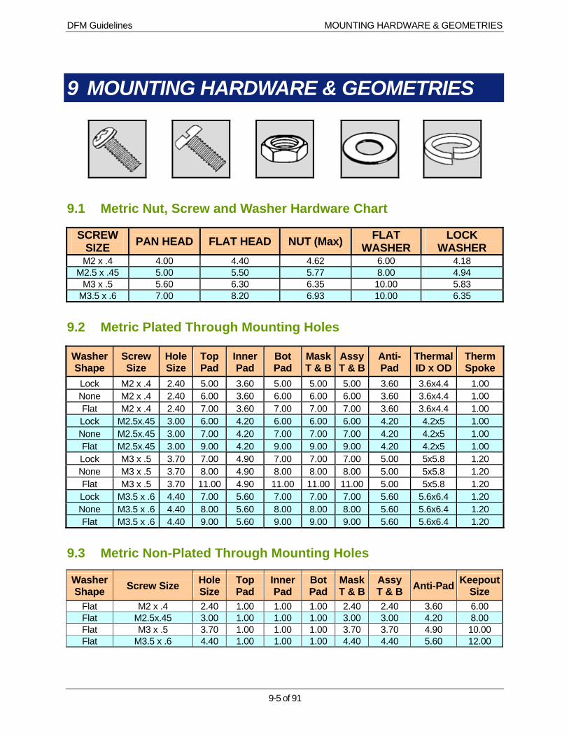
DFM Guidelines MOUNTING HARDWARE & GEOMETRIES
9-5 of 91
9 MOUNTING HARDWARE & GEOMETRIES
9.1 Metric Nut, Screw and Washer Hardware Chart
SCREW SIZE PAN HEAD FLAT HEAD NUT (Max) FLAT
WASHER LOCK
WASHER M2 x .4 4.00 4.40 4.62 6.00 4.18
M2.5 x .45 5.00 5.50 5.77 8.00 4.94 M3 x .5 5.60 6.30 6.35 10.00 5.83
M3.5 x .6 7.00 8.20 6.93 10.00 6.35
9.2 Metric Plated Through Mounting Holes
Washer Shape
Screw Size
Hole Size
Top Pad
Inner Pad
Bot Pad
Mask T & B
Assy T & B
Anti- Pad
Thermal ID x OD
Therm Spoke
Lock M2 x .4 2.40 5.00 3.60 5.00 5.00 5.00 3.60 3.6x4.4 1.00 None M2 x .4 2.40 6.00 3.60 6.00 6.00 6.00 3.60 3.6x4.4 1.00 Flat M2 x .4 2.40 7.00 3.60 7.00 7.00 7.00 3.60 3.6x4.4 1.00 Lock M2.5x.45 3.00 6.00 4.20 6.00 6.00 6.00 4.20 4.2x5 1.00 None M2.5x.45 3.00 7.00 4.20 7.00 7.00 7.00 4.20 4.2x5 1.00 Flat M2.5x.45 3.00 9.00 4.20 9.00 9.00 9.00 4.20 4.2x5 1.00 Lock M3 x .5 3.70 7.00 4.90 7.00 7.00 7.00 5.00 5x5.8 1.20 None M3 x .5 3.70 8.00 4.90 8.00 8.00 8.00 5.00 5x5.8 1.20 Flat M3 x .5 3.70 11.00 4.90 11.00 11.00 11.00 5.00 5x5.8 1.20 Lock M3.5 x .6 4.40 7.00 5.60 7.00 7.00 7.00 5.60 5.6x6.4 1.20 None M3.5 x .6 4.40 8.00 5.60 8.00 8.00 8.00 5.60 5.6x6.4 1.20 Flat M3.5 x .6 4.40 9.00 5.60 9.00 9.00 9.00 5.60 5.6x6.4 1.20
9.3 Metric Non-Plated Through Mounting Holes
Washer Shape Screw Size Hole
Size Top Pad
Inner Pad
Bot Pad
Mask T & B
Assy T & B Anti-Pad Keepout
Size Flat M2 x .4 2.40 1.00 1.00 1.00 2.40 2.40 3.60 6.00 Flat M2.5x.45 3.00 1.00 1.00 1.00 3.00 3.00 4.20 8.00 Flat M3 x .5 3.70 1.00 1.00 1.00 3.70 3.70 4.90 10.00 Flat M3.5 x .6 4.40 1.00 1.00 1.00 4.40 4.40 5.60 12.00

DFM Guidelines MOUNTING HARDWARE & GEOMETRIES
9-6 of 91
9.4 English Nut, Screw and Washer Hardware Chart
SCREW SIZE PAN HEAD FLAT HEAD NUT (Max) FLAT
WASHER LOCK
WASHER#2-48 4.24 4.36 5.51 6.35 4.36 #4-40 5.56 5.72 7.34 6.35 5.31 #6-32 6.85 7.08 9.17 8.13 6.35 #8-32 8.18 8.43 10.08 9.90 7.44
9.5 English Plated Through Mounting Holes
Washer Shape
Screw Size
Hole Size
Top Pad
Inner Pad
Bot Pad
Mask T & B
Assy T & B
Anti- Pad
Thermal ID x OD
Therm Spoke
Lock #2-48 2.80 5.00 4.00 5.00 5.00 5.00 4.00 4x4.8 1.00 None #2-48 2.80 6.00 4.00 6.00 6.00 6.00 4.00 4x4.8 1.00 Flat #2-48 2.80 7.00 4.00 7.00 7.00 7.00 4.00 4x4.8 1.00 Lock #4-40 3.20 5.00 4.40 5.00 5.00 5.00 4.40 4.4x5.2 1.00 None #4-40 3.20 6.00 4.40 6.00 6.00 6.00 4.40 4.4x5.2 1.00 Flat #4-40 3.20 7.00 4.40 7.00 7.00 7.00 4.40 4.4x5.2 1.00 Lock #6-32 4.00 6.00 5.20 6.00 6.00 6.00 5.20 5.2x6 1.20 None #6-32 4.00 7.00 5.20 7.00 7.00 7.00 5.20 5.2x6 1.20 Flat #6-32 4.00 9.00 5.20 9.00 9.00 9.00 5.20 5.2x6 1.20 Lock #8-32 4.70 9.00 5.90 9.00 9.00 9.00 6.00 6x7 1.40 None #8-32 4.70 10.00 5.90 10.00 10.00 10.00 6.00 6x7 1.40 Flat #8-32 4.70 11.00 5.90 11.00 11.00 11.00 6.00 6x7 1.40
9.6 English Non-Plated Through Mounting Holes
Washer Shape Screw Size Hole
Size Top Pad
Inner Pad
Bot Pad
Mask T & B
Assy T & B Anti-Pad Keepout
Size Flat #2-48 2.80 1.00 1.00 1.00 2.80 2.80 4.00 7.00 Flat #4-40 3.20 1.00 1.00 1.00 3.20 3.20 4.40 8.00 Flat #6-32 4.00 1.00 1.00 1.00 4.00 4.00 5.20 9.00 Flat #8-32 4.70 1.00 1.00 1.00 4.70 4.70 5.90 11.00

DFM Guidelines THROUGH-HOLE PADSTACKS
10-1 of 91
10 THROUGH-HOLE PADSTACKS
10.1 Plated Through-holes
Lead φ Finish Hole
Top Pad
Inner Pad
Bottom Pad
SolderMask Assy Plane
Anti-PadThermal ID x OD
Thermal Spoke
0.10 0.40 0.70 0.70 0.70 0.70 0.70 1.15 0.9x1.15 0.35 0.15 0.45 0.75 0.75 0.75 0.75 0.75 1.20 0.95x1.2 0.35 0.20 0.50 0.85 0.85 0.85 0.85 0.85 1.25 1x1.25 0.35 0.25 0.55 0.95 0.95 0.95 0.95 0.95 1.35 1.05x1.35 0.35 0.30 0.60 1.00 1.00 1.00 1.00 1.00 1.40 1.1x1.4 0.40 0.35 0.65 1.10 1.10 1.10 1.10 1.10 1.45 1.15x1.45 0.40 0.40 0.70 1.15 1.15 1.15 1.15 1.15 1.50 1.2x1.5 0.40 0.45 0.75 1.25 1.25 1.25 1.25 1.25 1.55 1.25x1.55 0.40 0.50 0.80 1.35 1.35 1.35 1.35 1.35 1.60 1.3x1.6 0.40 0.55 0.85 1.40 1.40 1.40 1.40 1.40 1.65 1.35x1.65 0.40 0.60 0.90 1.50 1.50 1.50 1.50 1.50 1.70 1.4x1.7 0.40 0.65 0.95 1.60 1.60 1.60 1.60 1.60 1.75 1.45x1.75 0.40 0.70 1.00 1.65 1.65 1.65 1.65 1.65 1.80 1.5x1.8 0.40 0.75 1.05 1.75 1.75 1.75 1.75 1.75 1.90 1.55x1.9 0.40 0.80 1.10 1.85 1.85 1.85 1.85 1.85 1.95 1.6x1.95 0.40 0.85 1.15 1.90 1.90 1.90 1.90 1.90 2.00 1.65x2 0.40 0.90 1.20 2.00 2.00 2.00 2.00 2.00 2.05 1.7x2.05 0.40 0.95 1.25 2.05 2.05 2.05 2.05 2.05 2.10 1.75x2.1 0.40 1.00 1.30 2.15 2.15 2.15 2.15 2.15 2.15 1.8x2.15 0.40 1.05 1.35 2.25 2.25 2.25 2.25 2.25 2.20 1.85x2.2 0.45 1.10 1.40 2.30 2.30 2.30 2.30 2.30 2.25 1.9x2.25 0.45 1.15 1.45 2.40 2.40 2.40 2.40 2.40 2.30 1.95x2.3 0.45 1.20 1.50 2.50 2.50 2.50 2.50 2.50 2.35 2x2.35 0.45 1.25 1.55 2.55 2.55 2.55 2.55 2.55 2.45 2.05x2.45 0.45 1.30 1.60 2.65 2.65 2.65 2.65 2.65 2.50 2.1x2.5 0.45 1.35 1.65 2.75 2.75 2.75 2.75 2.75 2.55 2.15x2.55 0.45 1.40 1.70 2.80 2.80 2.80 2.80 2.80 2.60 2.2x2.6 0.45 1.45 1.75 2.90 2.90 2.90 2.90 2.90 2.65 2.25x2.65 0.45 1.50 1.80 3.00 3.00 3.00 3.00 3.00 2.70 2.3x2.7 0.45 1.55 1.85 3.05 3.05 3.05 3.05 3.05 2.75 2.35x2.75 0.45 1.60 1.90 3.15 3.15 3.15 3.15 3.15 2.80 2.4x2.8 0.45 1.65 1.95 3.20 3.20 3.20 3.20 3.20 2.85 2.45x2.85 0.45 1.70 2.00 3.30 3.30 3.30 3.30 3.30 2.90 2.5x2.9 0.45
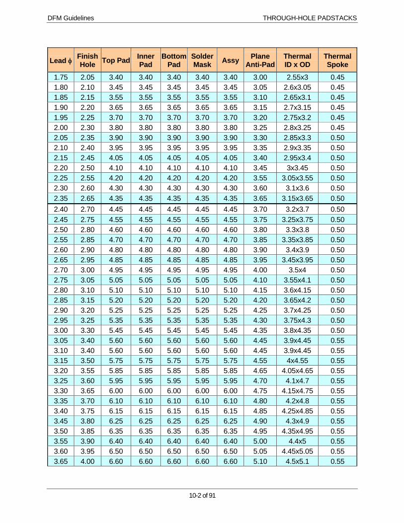
DFM Guidelines THROUGH-HOLE PADSTACKS
10-2 of 91
Lead φ Finish Hole Top Pad Inner
Pad Bottom
Pad SolderMask Assy Plane
Anti-PadThermal ID x OD
Thermal Spoke
1.75 2.05 3.40 3.40 3.40 3.40 3.40 3.00 2.55x3 0.45 1.80 2.10 3.45 3.45 3.45 3.45 3.45 3.05 2.6x3.05 0.45 1.85 2.15 3.55 3.55 3.55 3.55 3.55 3.10 2.65x3.1 0.45 1.90 2.20 3.65 3.65 3.65 3.65 3.65 3.15 2.7x3.15 0.45 1.95 2.25 3.70 3.70 3.70 3.70 3.70 3.20 2.75x3.2 0.45 2.00 2.30 3.80 3.80 3.80 3.80 3.80 3.25 2.8x3.25 0.45 2.05 2.35 3.90 3.90 3.90 3.90 3.90 3.30 2.85x3.3 0.50 2.10 2.40 3.95 3.95 3.95 3.95 3.95 3.35 2.9x3.35 0.50 2.15 2.45 4.05 4.05 4.05 4.05 4.05 3.40 2.95x3.4 0.50 2.20 2.50 4.10 4.10 4.10 4.10 4.10 3.45 3x3.45 0.50 2.25 2.55 4.20 4.20 4.20 4.20 4.20 3.55 3.05x3.55 0.50 2.30 2.60 4.30 4.30 4.30 4.30 4.30 3.60 3.1x3.6 0.50 2.35 2.65 4.35 4.35 4.35 4.35 4.35 3.65 3.15x3.65 0.50 2.40 2.70 4.45 4.45 4.45 4.45 4.45 3.70 3.2x3.7 0.50 2.45 2.75 4.55 4.55 4.55 4.55 4.55 3.75 3.25x3.75 0.50 2.50 2.80 4.60 4.60 4.60 4.60 4.60 3.80 3.3x3.8 0.50 2.55 2.85 4.70 4.70 4.70 4.70 4.70 3.85 3.35x3.85 0.50 2.60 2.90 4.80 4.80 4.80 4.80 4.80 3.90 3.4x3.9 0.50 2.65 2.95 4.85 4.85 4.85 4.85 4.85 3.95 3.45x3.95 0.50 2.70 3.00 4.95 4.95 4.95 4.95 4.95 4.00 3.5x4 0.50 2.75 3.05 5.05 5.05 5.05 5.05 5.05 4.10 3.55x4.1 0.50 2.80 3.10 5.10 5.10 5.10 5.10 5.10 4.15 3.6x4.15 0.50 2.85 3.15 5.20 5.20 5.20 5.20 5.20 4.20 3.65x4.2 0.50 2.90 3.20 5.25 5.25 5.25 5.25 5.25 4.25 3.7x4.25 0.50 2.95 3.25 5.35 5.35 5.35 5.35 5.35 4.30 3.75x4.3 0.50 3.00 3.30 5.45 5.45 5.45 5.45 5.45 4.35 3.8x4.35 0.50 3.05 3.40 5.60 5.60 5.60 5.60 5.60 4.45 3.9x4.45 0.55 3.10 3.40 5.60 5.60 5.60 5.60 5.60 4.45 3.9x4.45 0.55 3.15 3.50 5.75 5.75 5.75 5.75 5.75 4.55 4x4.55 0.55 3.20 3.55 5.85 5.85 5.85 5.85 5.85 4.65 4.05x4.65 0.55 3.25 3.60 5.95 5.95 5.95 5.95 5.95 4.70 4.1x4.7 0.55 3.30 3.65 6.00 6.00 6.00 6.00 6.00 4.75 4.15x4.75 0.55 3.35 3.70 6.10 6.10 6.10 6.10 6.10 4.80 4.2x4.8 0.55 3.40 3.75 6.15 6.15 6.15 6.15 6.15 4.85 4.25x4.85 0.55 3.45 3.80 6.25 6.25 6.25 6.25 6.25 4.90 4.3x4.9 0.55 3.50 3.85 6.35 6.35 6.35 6.35 6.35 4.95 4.35x4.95 0.55 3.55 3.90 6.40 6.40 6.40 6.40 6.40 5.00 4.4x5 0.55 3.60 3.95 6.50 6.50 6.50 6.50 6.50 5.05 4.45x5.05 0.55 3.65 4.00 6.60 6.60 6.60 6.60 6.60 5.10 4.5x5.1 0.55

DFM Guidelines THROUGH-HOLE PADSTACKS
10-3 of 91
Lead φ Finish Hole Top Pad Inner
Pad Bottom
Pad SolderMask Assy Plane
Anti-PadThermal ID x OD
Thermal Spoke
3.70 4.05 6.65 6.65 6.65 6.65 6.65 5.20 4.55x5.2 0.55 3.75 4.10 6.75 6.75 6.75 6.75 6.75 5.25 4.6x5.25 0.55 3.80 4.15 6.85 6.85 6.85 6.85 6.85 5.30 4.65x5.3 0.55 3.85 4.20 6.90 6.90 6.90 6.90 6.90 5.35 4.7x5.35 0.55 3.90 4.25 7.00 7.00 7.00 7.00 7.00 5.40 4.75x5.4 0.55 3.95 4.30 7.10 7.10 7.10 7.10 7.10 5.45 4.8x5.45 0.55 4.00 4.35 7.15 7.15 7.15 7.15 7.15 5.50 4.85x5.5 0.55 4.05 4.40 7.25 7.25 7.25 7.25 7.25 5.55 4.9x5.55 0.60 4.10 4.45 7.30 7.30 7.30 7.30 7.30 5.60 4.95x5.6 0.60 4.15 4.50 7.40 7.40 7.40 7.40 7.40 5.65 5x5.65 0.60 4.20 4.55 7.50 7.50 7.50 7.50 7.50 5.75 5.05x5.75 0.60 4.25 4.60 7.55 7.55 7.55 7.55 7.55 5.80 5.1x5.8 0.60 4.30 4.65 7.65 7.65 7.65 7.65 7.65 5.85 5.15x5.85 0.60 4.35 4.70 7.75 7.75 7.75 7.75 7.75 5.90 5.2x5.9 0.60 4.40 4.75 7.80 7.80 7.80 7.80 7.80 5.95 5.25x5.95 0.60 4.45 4.80 7.90 7.90 7.90 7.90 7.90 6.00 5.3x6 0.60 4.50 4.85 8.00 8.00 8.00 8.00 8.00 6.05 5.35x6.05 0.60 4.55 4.90 8.05 8.05 8.05 8.05 8.05 6.10 5.4x6.1 0.60 4.60 4.95 8.15 8.15 8.15 8.15 8.15 6.15 5.45x6.15 0.60 4.65 5.00 8.20 8.20 8.20 8.20 8.20 6.20 5.5x6.2 0.60
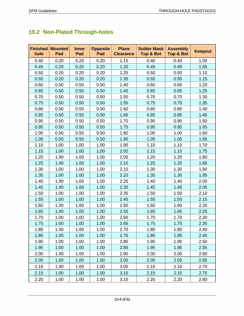
DFM Guidelines THROUGH-HOLE PADSTACKS
10-4 of 91
10.2 Non-Plated Through-holes
Finished hole
Mounted Pad
Inner Pad
Opposite Pad
Plane Clearance
Solder Mask Top & Bot
Assembly Top & Bot Keepout
0.40 0.20 0.20 0.20 1.15 0.40 0.40 1.00 0.45 0.20 0.20 0.20 1.20 0.45 0.45 1.05 0.50 0.20 0.20 0.20 1.25 0.50 0.50 1.10 0.55 0.20 0.20 0.20 1.35 0.55 0.55 1.15 0.60 0.50 0.50 0.50 1.40 0.60 0.60 1.20 0.65 0.50 0.50 0.50 1.45 0.65 0.65 1.25 0.70 0.50 0.50 0.50 1.50 0.70 0.70 1.30 0.75 0.50 0.50 0.50 1.55 0.75 0.75 1.35 0.80 0.50 0.50 0.50 1.60 0.80 0.80 1.40 0.85 0.50 0.50 0.50 1.65 0.85 0.85 1.45 0.90 0.50 0.50 0.50 1.70 0.90 0.90 1.50 0.95 0.50 0.50 0.50 1.75 0.95 0.95 1.55 1.00 0.50 0.50 0.50 1.80 1.00 1.00 1.60 1.05 0.50 0.50 0.50 1.90 1.05 1.05 1.65 1.10 1.00 1.00 1.00 1.95 1.10 1.10 1.70 1.15 1.00 1.00 1.00 2.00 1.15 1.15 1.75 1.20 1.00 1.00 1.00 2.05 1.20 1.20 1.80 1.25 1.00 1.00 1.00 2.10 1.25 1.25 1.85 1.30 1.00 1.00 1.00 2.15 1.30 1.30 1.90 1.35 1.00 1.00 1.00 2.20 1.35 1.35 1.95 1.40 1.00 1.00 1.00 2.25 1.40 1.40 2.00 1.45 1.00 1.00 1.00 2.30 1.45 1.45 2.05 1.50 1.00 1.00 1.00 2.35 1.50 1.50 2.10 1.55 1.00 1.00 1.00 2.45 1.55 1.55 2.15 1.60 1.00 1.00 1.00 2.50 1.60 1.60 2.20 1.65 1.00 1.00 1.00 2.55 1.65 1.65 2.25 1.70 1.00 1.00 1.00 2.60 1.70 1.70 2.30 1.75 1.00 1.00 1.00 2.65 1.75 1.75 2.35 1.80 1.00 1.00 1.00 2.70 1.80 1.80 2.40 1.85 1.00 1.00 1.00 2.75 1.85 1.85 2.45 1.90 1.00 1.00 1.00 2.80 1.90 1.90 2.50 1.95 1.00 1.00 1.00 2.85 1.95 1.95 2.55 2.00 1.00 1.00 1.00 2.90 2.00 2.00 2.60 2.05 1.00 1.00 1.00 3.00 2.05 2.05 2.65 2.10 1.00 1.00 1.00 3.05 2.10 2.10 2.70 2.15 1.00 1.00 1.00 3.10 2.15 2.15 2.75 2.20 1.00 1.00 1.00 3.15 2.20 2.20 2.80

DFM Guidelines THROUGH-HOLE PADSTACKS
10-5 of 91
Finished hole
Mounted Pad
Inner Pad
Opposite Pad
Plane Clearance
Solder Mask Top & Bot
Assembly Top & Bot Keepout
2.25 1.00 1.00 1.00 3.20 2.25 2.25 2.85 2.30 1.00 1.00 1.00 3.25 2.30 2.30 2.90 2.35 1.00 1.00 1.00 3.30 2.35 2.35 2.95 2.40 1.00 1.00 1.00 3.35 2.40 2.40 3.00 2.45 1.00 1.00 1.00 3.40 2.45 2.45 3.05 2.50 1.00 1.00 1.00 3.45 2.50 2.50 3.10 2.55 1.00 1.00 1.00 3.55 2.55 2.55 3.15 2.60 1.00 1.00 1.00 3.60 2.60 2.60 3.20 2.65 1.00 1.00 1.00 3.65 2.65 2.65 3.25 2.70 1.00 1.00 1.00 3.70 2.70 2.70 3.30 2.75 1.00 1.00 1.00 3.75 2.75 2.75 3.35 2.80 1.00 1.00 1.00 3.80 2.80 2.80 3.40 2.85 1.00 1.00 1.00 3.85 2.85 2.85 3.45 2.90 1.00 1.00 1.00 3.90 2.90 2.90 3.50 2.95 1.00 1.00 1.00 3.95 2.95 2.95 3.55 3.00 1.00 1.00 1.00 4.00 3.00 3.00 3.60 3.05 1.00 1.00 1.00 4.10 3.05 3.05 3.65 3.10 1.00 1.00 1.00 4.15 3.10 3.10 3.70 3.15 1.00 1.00 1.00 4.20 3.15 3.15 3.75 3.20 1.00 1.00 1.00 4.25 3.20 3.20 3.80 3.25 1.00 1.00 1.00 4.30 3.25 3.25 3.85 3.30 1.00 1.00 1.00 4.35 3.30 3.30 3.90 3.35 1.00 1.00 1.00 4.40 3.35 3.35 3.95 3.40 1.00 1.00 1.00 4.45 3.40 3.40 4.00 3.45 1.00 1.00 1.00 4.50 3.45 3.45 4.05 3.50 1.00 1.00 1.00 4.55 3.50 3.50 4.10 3.55 1.00 1.00 1.00 4.65 3.55 3.55 4.15 3.60 1.00 1.00 1.00 4.70 3.60 3.60 4.20 3.65 1.00 1.00 1.00 4.75 3.65 3.65 4.25 3.70 1.00 1.00 1.00 4.80 3.70 3.70 4.30 3.75 1.00 1.00 1.00 4.85 3.75 3.75 4.35 3.80 1.00 1.00 1.00 4.90 3.80 3.80 4.40 3.85 1.00 1.00 1.00 4.95 3.85 3.85 4.45 3.90 1.00 1.00 1.00 5.00 3.90 3.90 4.50 3.95 1.00 1.00 1.00 5.05 3.95 3.95 4.55 4.00 1.00 1.00 1.00 5.10 4.00 4.00 4.60 4.05 1.00 1.00 1.00 5.20 4.05 4.05 4.65 4.10 1.00 1.00 1.00 5.25 4.10 4.10 4.70 4.15 1.00 1.00 1.00 5.30 4.15 4.15 4.75 4.20 1.00 1.00 1.00 5.35 4.20 4.20 4.80 4.25 1.00 1.00 1.00 5.40 4.25 4.25 4.85 4.30 1.00 1.00 1.00 5.45 4.30 4.30 4.90

DFM Guidelines THROUGH-HOLE PADSTACKS
10-6 of 91
Finished hole
Mounted Pad
Inner Pad
Opposite Pad
Plane Clearance
Solder Mask Top & Bot
Assembly Top & Bot Keepout
4.35 1.00 1.00 1.00 5.50 4.35 4.35 4.95 4.40 1.00 1.00 1.00 5.55 4.40 4.40 5.00 4.45 1.00 1.00 1.00 5.60 4.45 4.45 5.05 4.50 1.00 1.00 1.00 5.65 4.50 4.50 5.10 4.55 1.00 1.00 1.00 5.75 4.55 4.55 5.15 4.60 1.00 1.00 1.00 5.80 4.60 4.60 5.20 4.65 1.00 1.00 1.00 5.85 4.65 4.65 5.25 4.70 1.00 1.00 1.00 5.90 4.70 4.70 5.30 4.75 1.00 1.00 1.00 5.95 4.75 4.75 5.35 4.80 1.00 1.00 1.00 6.00 4.80 4.80 5.40 4.85 1.00 1.00 1.00 6.05 4.85 4.85 5.45 4.90 1.00 1.00 1.00 6.10 4.90 4.90 5.50 4.95 1.00 1.00 1.00 6.15 4.95 4.95 5.55 5.00 1.00 1.00 1.00 6.20 5.00 5.00 5.60

DFM Guidelines VIA PADSTACKS
11-7 of 91
11 VIA PADSTACKS 11.1 Plated Through-Hole Vias
Material Condition Pad Hole Anti-Pad Solder
Mask Thermal
ID Thermal
OD Thermal Spoke
Minimum 0.40 0.20 0.65 0.00 0.50 0.65 0.20 Nominal 0.45 0.20 0.70 0.00 0.50 0.70 0.20
Maximum 0.50 0.20 0.75 0.00 0.50 0.75 0.20 Minimum 0.50 0.25 0.70 0.00 0.55 0.70 0.25 Nominal 0.55 0.25 0.75 0.00 0.55 0.75 0.25 Nominal 0.60 0.25 0.80 0.00 0.55 0.80 0.25
Maximum 0.65 0.25 0.85 0.00 0.55 0.85 0.30 Minimum 0.55 0.30 0.80 0.00 0.60 0.80 0.25 Nominal 0.60 0.30 0.85 0.00 0.65 0.85 0.25 Nominal 0.65 0.30 0.90 0.00 0.65 0.90 0.25
Maximum 0.70 0.30 0.95 0.00 0.70 0.95 0.30 Minimum 0.60 0.35 0.95 0.00 0.70 0.95 0.30 Nominal 0.65 0.35 1.00 0.00 0.75 1.00 0.30 Nominal 0.70 0.35 1.00 0.00 0.75 1.00 0.30
Maximum 0.75 0.35 1.05 0.00 0.80 1.05 0.35 Minimum 0.65 0.40 1.00 0.40 0.70 1.00 0.30 Nominal 0.70 0.40 1.05 0.40 0.75 1.05 0.30 Nominal 0.75 0.40 1.05 0.40 0.75 1.05 0.30
Maximum 0.80 0.40 1.10 0.40 0.80 1.10 0.35 Minimum 0.75 0.45 1.05 0.45 0.75 1.05 0.30 Nominal 0.80 0.45 1.15 0.45 0.85 1.15 0.35 Nominal 0.90 0.45 1.20 0.45 0.85 1.20 0.35
Maximum 0.95 0.45 1.25 0.45 0.95 1.25 0.35 Minimum 0.80 0.50 1.10 0.50 0.80 1.10 0.30 Nominal 0.85 0.50 1.20 0.50 0.90 1.20 0.35 Nominal 0.95 0.50 1.25 0.50 0.90 1.25 0.35
Maximum 1.00 0.50 1.30 0.50 1.00 1.30 0.40 Minimum 0.85 0.55 1.15 0.55 0.85 1.15 0.35 Nominal 0.90 0.55 1.20 0.55 0.95 1.20 0.35 Nominal 1.00 0.55 1.30 0.55 0.95 1.30 0.35
Maximum 1.05 0.55 1.35 0.55 1.05 1.35 0.40 Minimum 0.90 0.60 1.20 0.60 0.90 1.20 0.35 Nominal 0.95 0.60 1.25 0.60 1.00 1.25 0.35 Nominal 1.00 0.60 1.30 0.60 1.00 1.30 0.35
Maximum 1.10 0.60 1.40 0.60 1.10 1.40 0.40
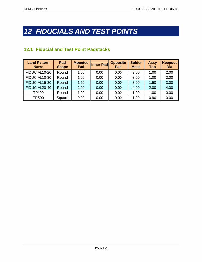
DFM Guidelines FIDUCIALS AND TEST POINTS
12-8 of 91
12 FIDUCIALS AND TEST POINTS
12.1 Fiducial and Test Point Padstacks
Land Pattern Name
Pad Shape
Mounted Pad Inner Pad Opposite
Pad Solder Mask
Assy Top
Keepout Dia
FIDUCIAL10-20 Round 1.00 0.00 0.00 2.00 1.00 2.00 FIDUCIAL10-30 Round 1.00 0.00 0.00 3.00 1.00 3.00 FIDUCIAL15-30 Round 1.50 0.00 0.00 3.00 1.50 3.00 FIDUCIAL20-40 Round 2.00 0.00 0.00 4.00 2.00 4.00
TP100 Round 1.00 0.00 0.00 1.00 1.00 0.00 TPS90 Square 0.90 0.00 0.00 1.00 0.90 0.00

DFM Guidelines UNDERWRITERS LABORATORIES INC. (UL) APPROVAL MARKING
13-9 of 91
13 UNDERWRITERS LABORATORIES INC. (UL) APPROVAL MARKING
13.1 Recognition and Flammability Ratings
UL recognition means that boards of specified base materials and design, and manufactured through identified processes, have been investigated by Underwriters Laboratories Inc. for thermal shock, bond strength and plating adhesion. Details of this investigation are in the UL 796, Standard for Printed Wiring Board s.
Flammability Classification
Flammability classification means that boards of specified base materials and design, manufactured through identified processes, have been investigated and classified by Underwriters Laboratories Inc., for flammability according to UL 94, Standard for Tests for Flammability for Parts in Devices and Appliances.
Design Guidelines
Each design should provide space on the outer layer for a UL recognized marking as described in the UL recognized Component Directory, UL Yellow Card, or UL report. It is the responsibility of the PCB manufacturer to mark the boards appropriately. The PCB designer must indicate the UL requirement either in their specifications and standards or on the drawing.

DFM Guidelines UNDERWRITERS LABORATORIES INC. (UL) APPROVAL MARKING
13-10 of 91
Lot Code Marking
If required by our customer, Wind River Systems may require that the PCB manufacturer provide a lot code. The Wind River Systems lot code is deciphered as follows:
5 06 10
0.65″
0.2″Mfg. Year
(1995)
Mfg. WeekCalendar Year
(Week 6)
Mfg. Day(Day 10)

DFM Guidelines RoHS COMPLIANCE
14-11 of 91
14 RoHS COMPLIANCE
14.1 Limitation Hazardous materials such as Lead and Mercury to be less than 0.1% of weight in the raw materials
14.2 Exemptions None
14.3 Solder Material SnAgCu (Tin, Silver and Copper)
14.4 Board Substrate Lead free presumed
14.5 Component Labeling Lead Presence [[Pb]]
Non presence [[G]]
14.6 Process parameters MST or MSL
14.7 Lead Free Symbol

DFM Guidelines GUIDELINES FOR TOOLING INTERFACE
15-12 of 91
15 GUIDELINES FOR TOOLING INTERFACE The successful transformation of printed circuit board design data into manufacturing tools depends on the quality of the data received and the quality of decisions made in its interpretation. This process is complicated by a wide variety of data communication styles and format.
We strongly recommend that system compatibility and data-set completeness be reviewed and tested before production tooling. Sending a complete “non-production” part design through the tooling process reduces the possibility that production will be delayed when time is critical.
Along with a description of the minimum requirements, more specific guidance is offered regarding data options and preferences in the form of tooling capability classes. Below is a brief explanation of the meaning of each of these classes.
15.1 Tooling Capability Classification
PREFERRED
Part data whose characteristics facilitate smoother, high quality tooling design processing. The part data sets that fall into this category minimize the risk of miscommunication because they require less human interpretation, allow greater process automation, have reduced data volumes, and use simpler communication protocols.
ACCEPTABLE
Part data whose characteristics are less than optimum, but are within our normal tooling design capability.
STRONGLY DISCOURAGED
Part data whose characteristics push the limits or fall outside the range of our normal tooling design capability. Because of the increased demand on our resources and the increased risk of communication failure, the tooling of these parts must be negotiated with the Project Manager.
Wind River Systems is a strong advocate of the ODB++ data format for exchanging circuit board design information. This standard format contains all image and NC data in a single integrated file. The highly defined structure of this data format streamlines design-to-manufacturing communication by eliminating the need for the coordination of multiple files and interpretation of vendor-specific data formats.

DFM Guidelines GUIDELINES FOR TOOLING INTERFACE
15-13 of 91
IMAGE DATA
The image data is a graphic description of the part used to create the photo-tools. The minimum requirements for tooling image data are:
1. A clear description of the function of each file in a “Readme.txt” file.
2. Image file merging, if required, must be clearly described.
3. If Gerber RS-274x format is used.
PREFERRED
• ODB++ format
• Gerber data in RS-274X format
• IPC-356 Netlist used for Gerber netlist to CAD data netlist comparison
• File function described in explanatory documentation
• Pads “flashed” with standard aperture shapes rather than “painted” with lines.
• Solder mask pads the same size as the outer layer pads allowing easy modification to manufacturing specifications.
• Direct transfer of the original CAD system aperture table file, allowing automated translation of aperture data.
• ASCII data code.
ACCEPTABLE
• “Painted” pads
• Image files not in alignment
• “Standard aperture” table to be used for all parts. Part specific deviations communicated via the job order.
• Aperture table with each order that is not machine readable
• File function described with naming convention or explanatory documentation
• EBCDIC data code

DFM Guidelines GUIDELINES FOR TOOLING INTERFACE
15-14 of 91
STRONGLY DISCOURAGED
• Missing or ambiguous data
• Multiple aperture tables
• Custom editing of conductive features
• Very large files, usually caused by inefficient “painting” of image fill areas
• Format other than Gerber or IPC-350
PROFILE DATA
The route profile program is created by interpreting the part’s fabrication drawing. This drawing must clearly and fully describe the part profile using standard dimensioning and tolerancing practices. It must also provide a dimensional reference to at least one drilled hole internal to the part.
PREFERRED
• Drawing files supplied in Adobe PDF format.
ACCEPTABLE • Drawing files supplied in Gerber, IGES or DXF (v.11 or earlier) format, fully
tested before use.
STRONGLY DISCOURAGED • Paper fabrication drawing
• Plotter compatibility not fully tested before use
• Incomplete dimensioning of the part
DRILL DATA
Wind River Systems uses the drill program provided as a master from which the production drill program is produced. The minimum requirements for tooling drill data are:
1. At least one file describing the location of all holes internal to the part.
2. A drill shop report must be provided that includes the following information for each hole size:
• Finished hole size
• Finished hole-size tolerance
• Hole count
• Hole plating status
DFM Guidelines GUIDELINES FOR TOOLING INTERFACE
15-15 of 91
A drawing of drilled hole locations should be provided which represents each drilled hole size with a unique symbol or letter to verify the correctness of the drill data.
PREFERRED • Drill data provided in Excellon format 2 or IPC-350 format
• The order of holes drill shop report matches the order in the drill data
• Drill data aligns with image data
• ASCII data code
ACCEPTABLE
• Drill data supplied in Gerber format
• EBCDIC or EIA code
STRONGLY DISCOURAGED
• Paper tape
• A plot for the drilled holes is not provided
MEDIA OPTIONS
PREFERRED
Part data supplied using one of the following media:
• CD-ROM
STRONGLY DISCOURAGED
Part data supplied using one of the following media:
• Paper tape
• Image data supplied with filmwork only
• Other media

DFM Guidelines GUIDELINES FOR TOOLING INTERFACE
15-16 of 91
DATA COMPRESSION OPTIONS
If data compression is used, a description of the compression technique used should be included in the data set.
PREFERRED
Part data supplied in one of the following data compression formats:
• pkzip (MS-DOS, SUN)
• tar (UNIX)
• cpio (UNIX) • compress (SUN)
• bar (SUN)
STRONGLY DISCOURAGED
• Part data supplied using other data compression formats

WRS01-00-XXX 17 of 91 v0.05 Confidential 21 Aug 2003