Embed Size (px)
Citation preview
7/27/2019 Design Library Master Training_cr
http://slidepdf.com/reader/full/design-library-master-trainingcr 1/89
7/27/2019 Design Library Master Training_cr
http://slidepdf.com/reader/full/design-library-master-trainingcr 2/89
The ZUKEN logo and CI mark are registered trademarks of Zuken, Inc.
CR-5000, System Designer, Board Designer, PWS, Package Synthesizer and Lightning are
trademarks or registered trademarks of Zuken, Inc.
The other company names and product names are trademarks or registered trademarks of each
company.
◆This manual was prepared as an educational text.
For details on specific product features, refer to “Online
Documentation”.
◆The contents of this manual are subject to change without notice.
◆Copying the contents of this manual without permission from Zuken
Inc. is prohibited by law.
© 2007 ZUKEN Incorporated.
7/27/2019 Design Library Master Training_cr
http://slidepdf.com/reader/full/design-library-master-trainingcr 3/89
Preface - 1
Preface Welcome to the world of thePCB Design Library
Preface
The Master Training <PCB Design Library> is designed to provide you knowledge
required and operation about registration and management for libraries except
component which use for PCB design. This is an essential training course tounderstand in depth the whole system of the CR-5000 system.
Beginner’s Training
Master Training
Users engaged only in library design and management should study up through
Library but we also recommend reading Board Design. Users only engaged in board
design are expected to mainly study Board Design but are recommended to previouslyread and try out Library.
Beginner’s Training
<PCB Design>
The aim is to attain a level where you
can help operators.
You will learn the flow of board design.
Simple operations for PCB design
The aim is to attain the knowledge
necessary to be an operator.
Library Board Design
Master Training<Component Library>
Registration and management of libraries
Master Training
<PCB Design Library>
Registration and management of PCBdesign libraries
Master Training<PCB Design>
Detailed operation for PCB design
Master Training
<CAM>
Operation for manufacturing paneldesign through CAM output
Master Training
<EngineeringChange/Operation>
Operation and knowledge related toengineering design change/operation
7/27/2019 Design Library Master Training_cr
http://slidepdf.com/reader/full/design-library-master-trainingcr 4/89
Contents
Preface Welcome to the world of the PCB Design Library
Chapter 1 Using PCB Design Library Tool For The First Time
1. Overview of the Lesson ................................................................................................1-1
Chapter 2 The PCB Design Library
1. The PCB Design Library ...............................................................................................2-1
2. Resource Files..............................................................................................................2-3
Resource files ................................................................................................................................2-3
Resource files for each tool............................................................................................................2-4
Managing the PCB library list file (library.rsc).................................................................................2-5
Editing the PCB library list file (library.rsc)......................................................................................2-7
Chapter 3 Technology Library
1. Registering a Technology Library..................................................................................3-1
Technology library ..........................................................................................................................3-1
Starting up the Technology Editor...................................................................................................3-4
* Resource file................................................................................................................................3-5
Registering technology...................................................................................................................3-6
* Edit Layer Mapping ....................................................................................................................3-17
* Items which can be set from menu bar ......................................................................................3-20
2. Operating the Technology Library ...............................................................................3-22
Specifications According to Destination........................................................................................3-22
Using a Single-Side Board ...........................................................................................................3-24
Determining Footprint Layer and PCB Layer................................................................................3-25

7/27/2019 Design Library Master Training_cr
http://slidepdf.com/reader/full/design-library-master-trainingcr 5/89
Chapter 4 Design Rule Library
1. Registering a Design Rule Library ................................................................................4-1
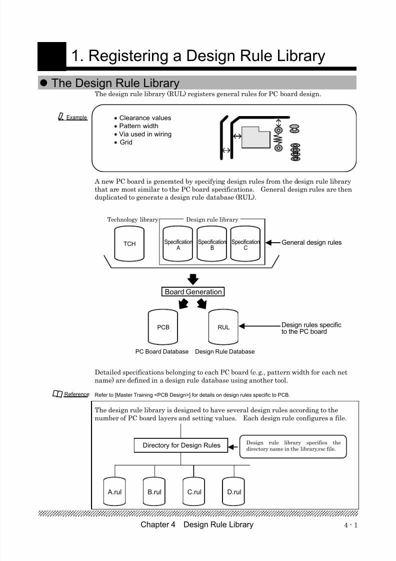
The Design Rule Library.................................................................................................................4-1
Starting up the Design Rule Library Edit Tool .................................................................................4-2* Resource files. .............................................................................................................................4-2
* Footprint specification name........................................................................................................4-5
* Loading existing design rules.......................................................................................................4-6
* Define search key ........................................................................................................................4-8
Defining Design Rules....................................................................................................................4-9
* The setting method for each item...............................................................................................4-24
Appendix1. Design Rule Unit Setting Value List ............................................................................. A-1
7/27/2019 Design Library Master Training_cr
http://slidepdf.com/reader/full/design-library-master-trainingcr 6/89
7/27/2019 Design Library Master Training_cr
http://slidepdf.com/reader/full/design-library-master-trainingcr 7/89
1 - 1
1. Overview of the Lesson
Chapter 1 Using PCB Design Library Tool For The First Time
The Master Training <PCB Design Library> introduces you to the operations for thefunctions and registering methods for libraries (Technology Library and Design RuleLibrary) that are necessary in board designing.
These files are in the part surrounded by a dotted line in the figure below.
This chapter explains the workflow todesign a PC board using the CR-5000 anddescribes required items and knowledgebefore starting the actual designing.
Refer to [Chapter 2 The PCB Design Library].
This chapter explains how to prepareconductive layers, symbol mark layers,user defined layers and other itemsrequired by a library for PC board design.
It also shows how to specify layers inwhich component shapes to be read to theboard are included.
Refer to [Chapter 3 Technology Library].
This chapter explains how to extractgeneral rules from design rulesnecessary for PC board design andprepare them as a library in advance.
Refer to [Chapter 4 Design Rule Library].
• Design flow
• Required items
• Resource files
Design RuleDatabase
PC BoardDatabase
• Clearance values
• Pattern width
• Via used in wiring
• Grid
Four-layerboard A
Two-layerboard
Four-layerboard B
RUL PCB
PRT PKG FTP
CDB
NDF RUF
Net Rule
System Designer TechnologyLibrary
Design RuleLibrary
ruleA ruleB
What is the PCB Desi n Librar ?
Re isterin in the Technolo Librar
Registering in the Design Rule Library
Reference
Reference
Reference
7/27/2019 Design Library Master Training_cr
http://slidepdf.com/reader/full/design-library-master-trainingcr 8/89
7/27/2019 Design Library Master Training_cr
http://slidepdf.com/reader/full/design-library-master-trainingcr 9/89
2 - 1Chapter 2 The PCB Design Library
1. The PCB Design Library
The following flowchart shows the workflow of PCB design using the CR-5000.
Registering a Component Library (CDB)
Registering a Design Rule Library
Refer to "Master Training (Component Library)."
These procedures are introduced in this manual.
Library registration
Generating a PC Board Database(Editing PC board-dedicated design rules) PC board design
Inputting PC Board Shape
Trial Placement of Components
Placement of Components
Wiring
Inputting Manufacturing Data
Check
Refer to "Master Training (PCB Design)."
Paneling
Outputting CAM
Refer to "Master Training (CAM)."
Registering a Technology Library
Reference
Reference
Reference
7/27/2019 Design Library Master Training_cr
http://slidepdf.com/reader/full/design-library-master-trainingcr 10/89
2 - 2 Chapter 2 The PCB Design Library
1. The PCB Design Library
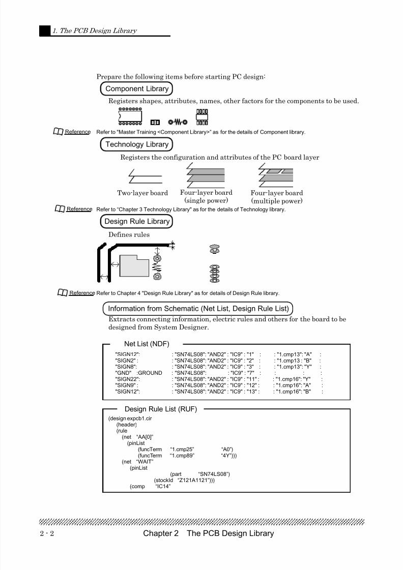
Prepare the following items before starting PC design:
Registers shapes, attributes, names, other factors for the components to be used.
Refer to "Master Training <Component Library>” as for the details of Component library.
Registers the configuration and attributes of the PC board layer
Refer to “Chapter 3 Technology Library" as for the details of Technology library.
Defines rules
Refer to Chapter 4 "Design Rule Library" as for details of Design Rule library.
Extracts connecting information, electric rules and others for the board to bedesigned from System Designer.
Component Library
Technology Library
Design Rule Library
Information from Schematic (Net List, Design Rule List)
Reference
Reference
Reference
"SIGN12": : "SN74LS08": "AND2" : "IC9" : "1" : : "1.cmp13": "A" :"SIGN2" : : "SN74LS08": "AND2" : "IC9" : "2" : : "1.cmp13 : "B" :"SIGN8": : "SN74LS08": "AND2" : "IC9" : "3" : : "1.cmp13": "Y" :"GND" :GROUND : "SN74LS08": : "IC9" : "7" : : : :"SIGN22": : "SN74LS08": "AND2" : "IC9" : "11" : : "1.cmp16": "Y" :"SIGN9" : : "SN74LS08": "AND2" : "IC9" : "12" : : "1.cmp16": "A" :"SIGN12": : "SN74LS08": "AND2" : "IC9" : "13" : : "1.cmp16": "B" :
Net List (NDF)
(design expcb1.cir(header)(rule
(net “AA[0]”(pinList
(funcTerm “1.cmp25” “A0”)(funcTerm “1.cmp89” “4Y”)))
(net “WAIT”(pinList
(part “SN74LS08”)(stockId “Z121A1121”)))
(comp “IC14”
Design Rule List (RUF)
Two-layer board Four-layer board
(single power)
Four-layer board
(multiple power)
7/27/2019 Design Library Master Training_cr
http://slidepdf.com/reader/full/design-library-master-trainingcr 11/89
2 - 3Chapter 2 The PCB Design Library
2. Resource Files
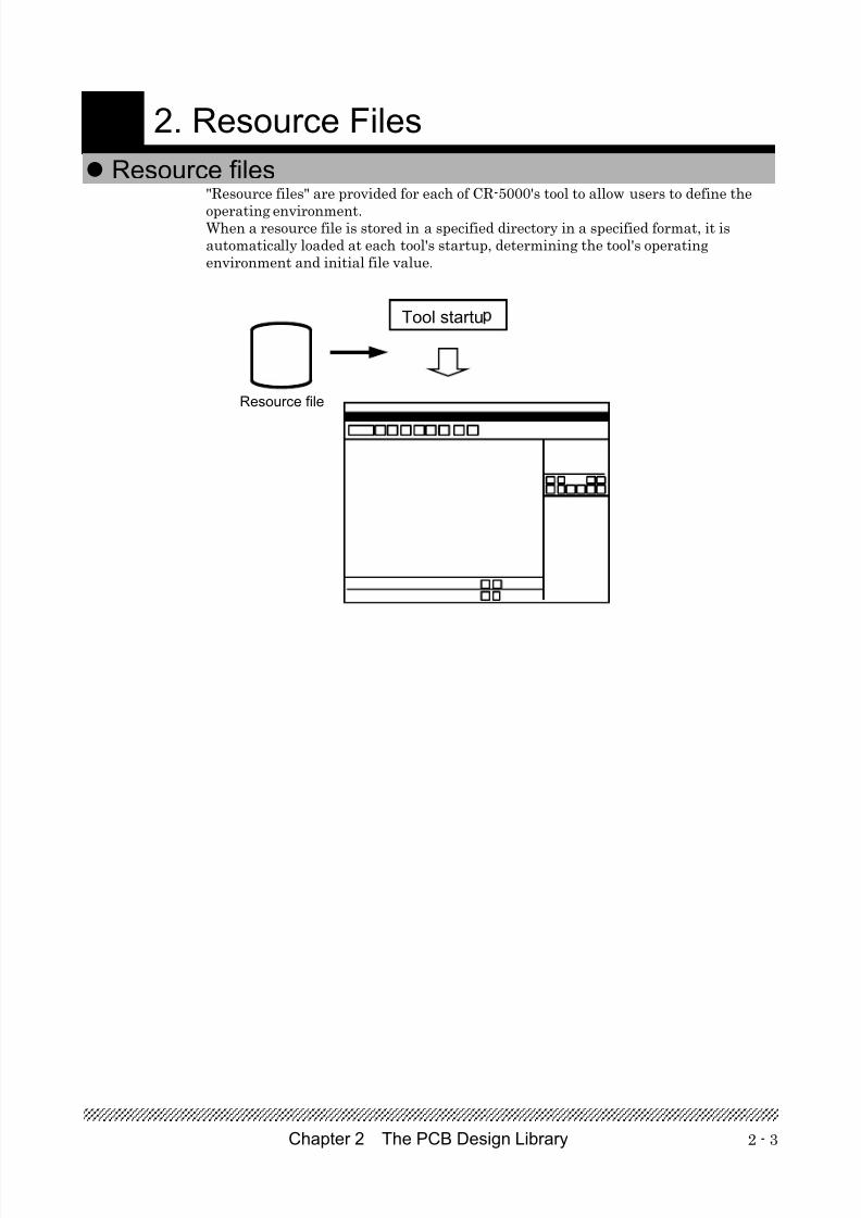
Resource files"Resource files" are provided for each of CR-5000's tool to allow users to define the
operating environment.When a resource file is stored in a specified directory in a specified format, it isautomatically loaded at each tool's startup, determining the tool's operatingenvironment and initial file value.
Tool startu
Resource file

7/27/2019 Design Library Master Training_cr
http://slidepdf.com/reader/full/design-library-master-trainingcr 12/89
2 - 4 Chapter 2 The PCB Design Library
2. Resource Files
The PCB library references the following resource files:
Library Resource
Priority 1 %HOME%\cr5000\ue\library.rsc (local resource)Priority 2 %CR5_PROJECT_ROOT%\zue\info\library.rsc (project resource)Priority 3 %ZUEROOT%\info\library.rsc (master resource)
Sets file names and storage directories for libraries required in designing, including the components library,technology library, design rule library, and manufacturing rule library.
Differences in roles and usage among the above libraries are shown below.
The environment variables shown above (e.g. %ZUEROOT%) are shown as they appear in Windows.In UNIX, they are represented in the form $ZUEROOT.(e.g. Parameter definition resource for PCB/PNL data generation: $ZUEROOT/info/parameter.rsc)
The followings are items in a library resource (library.rsc) referenced by a PCB designlibrary.
Only one library file name can be set for one type of library. Even if a file name for one library type is written intwo or more columns, all descriptions after the first are ignored.
Resource files for each tool
Caution
Caution
Componentlibraries
7/27/2019 Design Library Master Training_cr
http://slidepdf.com/reader/full/design-library-master-trainingcr 13/89
2 - 5Chapter 2 The PCB Design Library
2. Resource Files
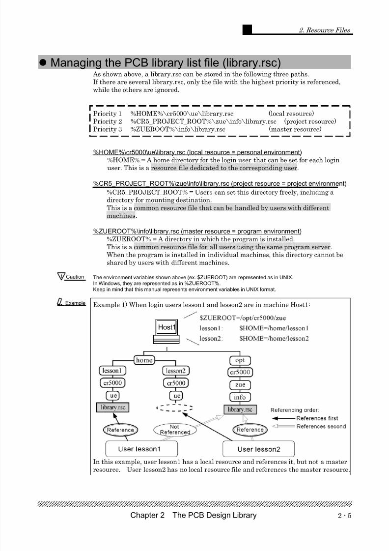
As shown above, a library.rsc can be stored in the following three paths.If there are several library.rsc, only the file with the highest priority is referenced,while the others are ignored.
Priority 1 %HOME%\cr5000\ue\library.rsc (local resource)Priority 2 %CR5_PROJECT_ROOT%\zue\info\library.rsc (project resource)Priority 3 %ZUEROOT%\info\library.rsc (master resource)
%HOME%\cr5000\ue\library.rsc (local resource = personal environment)%HOME% = A home directory for the login user that can be set for each loginuser. This is a resource file dedicated to the corresponding user.
%CR5_PROJECT_ROOT%\zue\info\library.rsc (project resource = project environment)
%CR5_PROJECT_ROOT% = Users can set this directory freely, including adirectory for mounting destination.This is a common resource file that can be handled by users with differentmachines.
%ZUEROOT%\info\library.rsc (master resource = program environment)%ZUEROOT% = A directory in which the program is installed.This is a common resource file for all users using the same program server.When the program is installed in individual machines, this directory cannot beshared by users with different machines.
The environment variables shown above (ex. $ZUEROOT) are represented as in UNIX.In Windows, they are represented as in %ZUEROOT%.
Keep in mind that this manual represents environment variables in UNIX format.
Example 1) When login users lesson1 and lesson2 are in machine Host1:
In this example, user lesson1 has a local resource and references it, but not a masterresource. User lesson2 has no local resource file and references the master resource.
Managing the PCB library list file (library.rsc)
Caution
Example
Host1
7/27/2019 Design Library Master Training_cr
http://slidepdf.com/reader/full/design-library-master-trainingcr 14/89
2 - 6 Chapter 2 The PCB Design Library
2. Resource Files
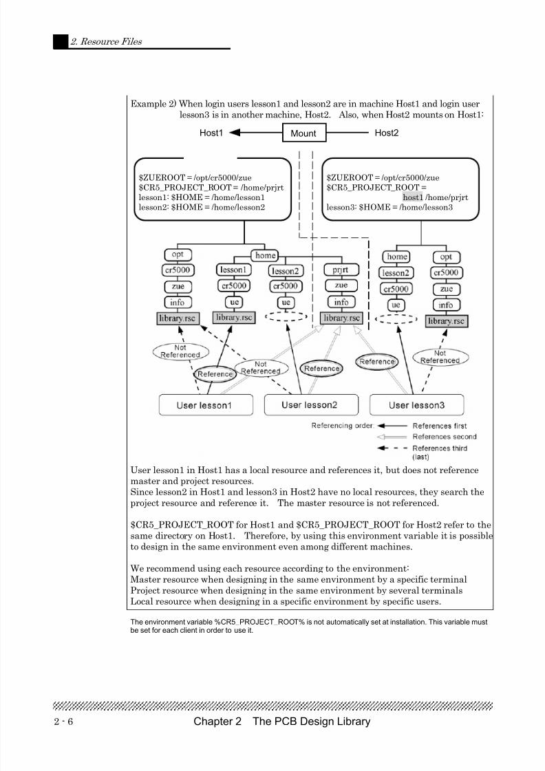
Example 2) When login users lesson1 and lesson2 are in machine Host1 and login userlesson3 is in another machine, Host2. Also, when Host2 mounts on Host1:
User lesson1 in Host1 has a local resource and references it, but does not referencemaster and project resources.Since lesson2 in Host1 and lesson3 in Host2 have no local resources, they search theproject resource and reference it. The master resource is not referenced.
$CR5_PROJECT_ROOT for Host1 and $CR5_PROJECT_ROOT for Host2 refer to the
same directory on Host1. Therefore, by using this environment variable it is possibleto design in the same environment even among different machines.
We recommend using each resource according to the environment:Master resource when designing in the same environment by a specific terminalProject resource when designing in the same environment by several terminalsLocal resource when designing in a specific environment by specific users.
The environment variable %CR5_PROJECT_ROOT% is not automatically set at installation. This variable mustbe set for each client in order to use it.
Host1 Host2Mount
$ZUEROOT = /opt/cr5000/zue$CR5_PROJECT_ROOT =
host1 /home/prjrtlesson3: $HOME = /home/lesson3
$ZUEROOT = /opt/cr5000/zue$CR5_PROJECT_ROOT = /home/prjrtlesson1: $HOME = /home/lesson1lesson2: $HOME = /home/lesson2
7/27/2019 Design Library Master Training_cr
http://slidepdf.com/reader/full/design-library-master-trainingcr 15/89
2 - 7Chapter 2 The PCB Design Library
2. Resource Files
The library.rsc file can be edited with the "PCB design library list file editor", as wellas by the UNIX vi editor and the Word Pad for Windows. This section shows how toedit the library.rsc using the PCB design library list file editor.
The PCB design library list file editor can edit all types of library.rsc for the masterresource (program environment), project resource (project environment) and localresource (personal environment).
Edit a personal environment library.rsc prepared for the lesson, according to the lessonenvironment.
Resource file to be edited%HOME%/cr5000/ue/library.rsc (local resource = personal environment)
(C:\home\lesson2)
Library to be referenced (library has already been prepared)• Part library C:\home\lesson2\cdb\cdb2.prt• Package library C:\home\lesson2\cdb\cdb2.pkg• Footprint library C:\home\lesson2\cdb\cdb2.ftp• Technology library C:\home\lesson2\tch\lay.tch• Design rule library C:\home\lesson2\rule.rul
Start up the PCB design library list file editor.
1. Start up the editor by clicking the start button on the task bar, then select Programs ⇒
CR-5000 Board Designer 10.0 ⇒ Utilities ⇒PCB Design Library List File Editor from the menu.
1. Start up the editor by clicking Utilities ⇒ PCB library list file editor on the menu.
Editing the PCB library list file (library.rsc)
Lesson
UNIX
Click
7/27/2019 Design Library Master Training_cr
http://slidepdf.com/reader/full/design-library-master-trainingcr 16/89
2 - 8 Chapter 2 The PCB Design Library
2. Resource Files
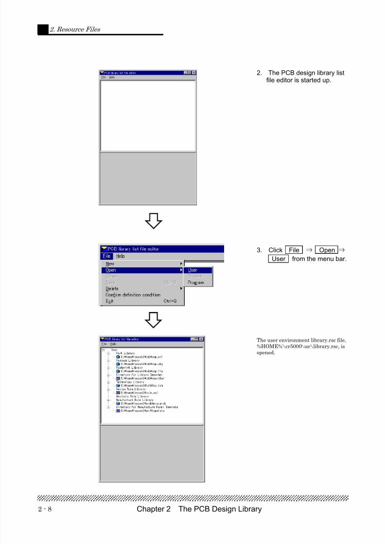
2. The PCB design library listfile editor is started up.
3. Click File ⇒ Open ⇒
User from the menu bar.
The user environment library.rsc file,%HOME%\cr5000\ue\library.rsc, isopened.
7/27/2019 Design Library Master Training_cr
http://slidepdf.com/reader/full/design-library-master-trainingcr 17/89
2 - 9Chapter 2 The PCB Design Library
2. Resource Files
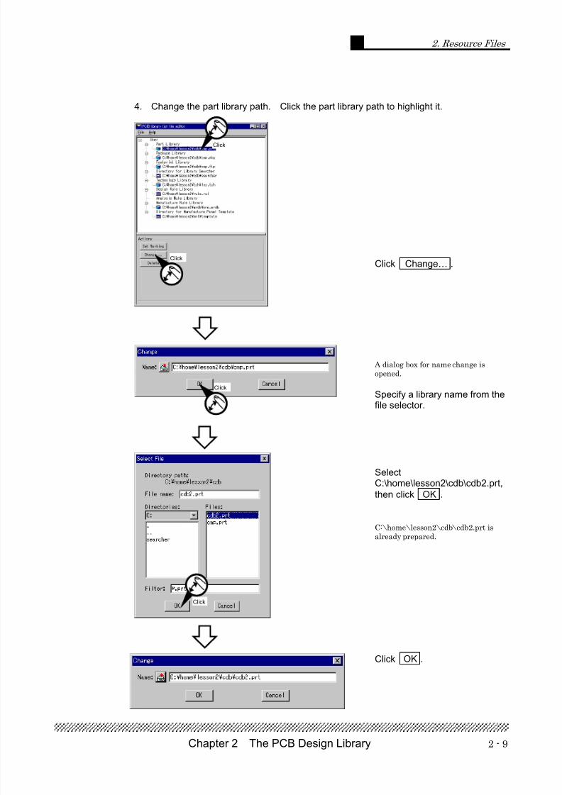
4. Change the part library path. Click the part library path to highlight it.
Click Change… .
A dialog box for name change isopened.
Specify a library name from thefile selector.
SelectC:\home\lesson2\cdb\cdb2.prt,then click OK .
C:\home\lesson2\cdb\cdb2.prt isalready prepared.
Click OK .
Click
Click
Click
Click
7/27/2019 Design Library Master Training_cr
http://slidepdf.com/reader/full/design-library-master-trainingcr 18/89
2 - 10 Chapter 2 The PCB Design Library
2. Resource Files
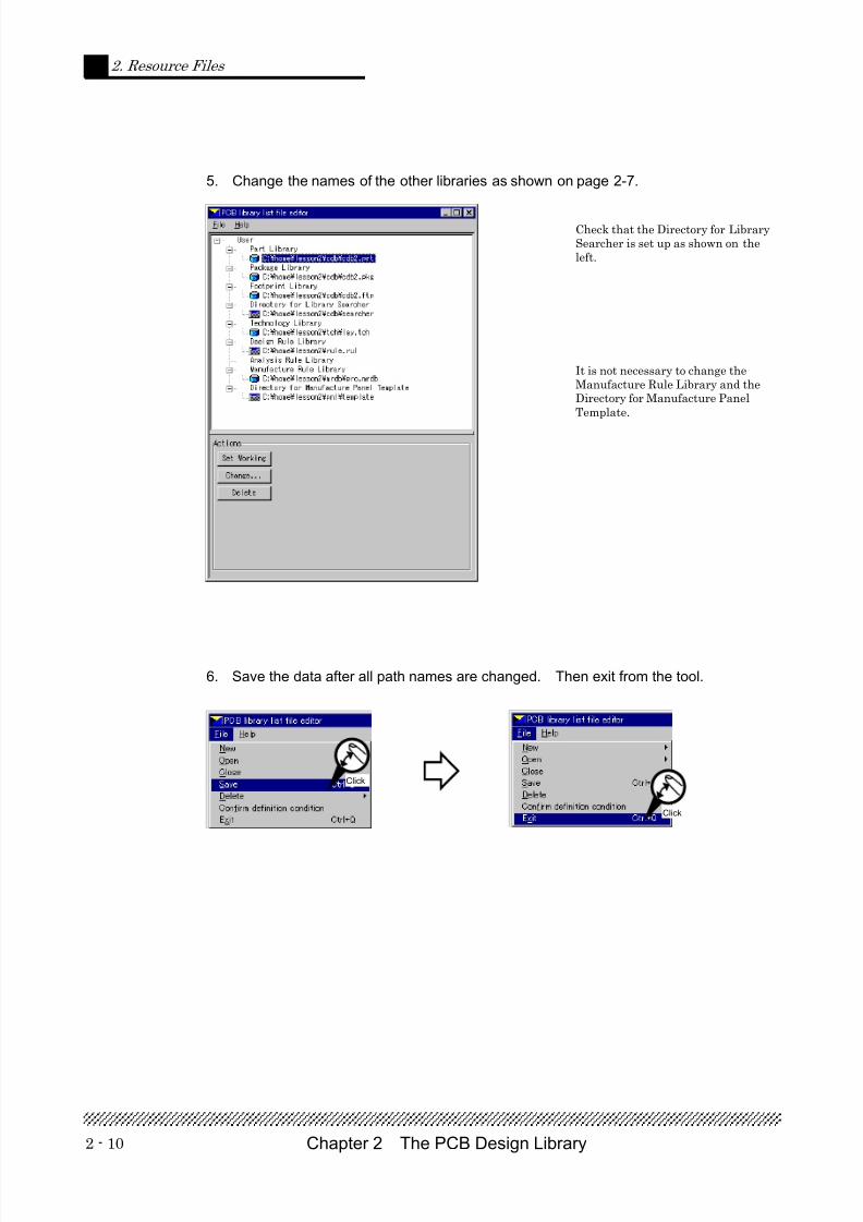
5. Change the names of the other libraries as shown on page 2-7.
Check that the Directory for LibrarySearcher is set up as shown on theleft.
It is not necessary to change theManufacture Rule Library and theDirectory for Manufacture PanelTemplate.
6. Save the data after all path names are changed. Then exit from the tool.
Click
Click
7/27/2019 Design Library Master Training_cr
http://slidepdf.com/reader/full/design-library-master-trainingcr 19/89
7/27/2019 Design Library Master Training_cr
http://slidepdf.com/reader/full/design-library-master-trainingcr 20/89
7/27/2019 Design Library Master Training_cr
http://slidepdf.com/reader/full/design-library-master-trainingcr 21/89
Chapter 3 Technology Library3 - 2
1. Registering a Technology Library
Now, please recall the footprint layer definition described in "Registering aComponent Library (CDB)". A layer for the component registration called "footprint layer" is also defined in the
CDB library, and the objects are input to each footprint layer.
Layers must be defined for this footprint layer so that it can be used for any board,regardless of the number of layers on the board to be designed.
Therefore, the footprint layer which is defined separately, must be assigned to thePCB layer to use the component in the PC board. The technology library assigns thefootprint layers to PCB layers, too.
Correspondence between the footprint and PCB layers is referred to as Layer
Mapping . As shown above, a footprint can correspond with any PCB layers, including 2-layerand 4-layer boards.
Example
A side conductive layer
B side conductive layer
Inner conductive layer
Resist layer
Symbol mark layer
Hole layer
Component side conductive layer
Solder side conductive layer
Inner conductive layer
Footprint Layer
Conductive layer1
Conductive layer2
2-Layer Board
Conductive layer1
Conductive layer2
Conductive layer3
Conductive layer4
4-Layer Board
Layer Mapping
7/27/2019 Design Library Master Training_cr
http://slidepdf.com/reader/full/design-library-master-trainingcr 22/89
3 - 3Chapter 3 Technology Library
1. Registering a Technology Library
When registering a footprint layer, component shapes are registered from a view of thecomponent side. When inputting components into the PC board, however, theobject's input layer varies depending on whether the placement side is Side A or B.
For this reason, the Technology Library makes it possible to change the input layer bydefining Side A mappings and Side B mappings. When a shape does not change even ifthe placement side changes, an object-input layer is switched automatically bychanging the mapping for each placement side, without having to create anotherfootprint. When placing on Side B, a footprint is mirror-inverted automatically todesign the PC board from the component side.
As a resist shape may be changed when a placement side changes, the resist shape canbe changed with the same footprint if the footprint-layer definition and mapping are
used well.
For detailed information on operation using mapping, “2. Operating the Technology Library” on page 3-22 will beexplained.
Conductive
Resist
Symbol mark
Layer1(A side)
Layer2(B side)
Resist(A side)
Resist(B side)
Symbol(A side)
Symbol(B side)
Footprint Layer
PCB Layer A-side placement
B-side placement
When placed on A-side
When placed on B-side
Footprint
Reference
7/27/2019 Design Library Master Training_cr
http://slidepdf.com/reader/full/design-library-master-trainingcr 23/89
Chapter 3 Technology Library3 - 4
1. Registering a Technology Library
The Technology Editor is used to register the technology library.This section explains what kind of information will be registered to the technology
library, through the lesson.
1. Before starting up the Technology Editor, be sure to check whether the names of thetechnology library files to be registered and component library file to be referenced aredefined correctly in the resource file. A local library resource is used in this lesson.
For detailed information on how to define and edit the resource file, refer to "Editing PCB design library list file(library.rsc)" on page 2-7.
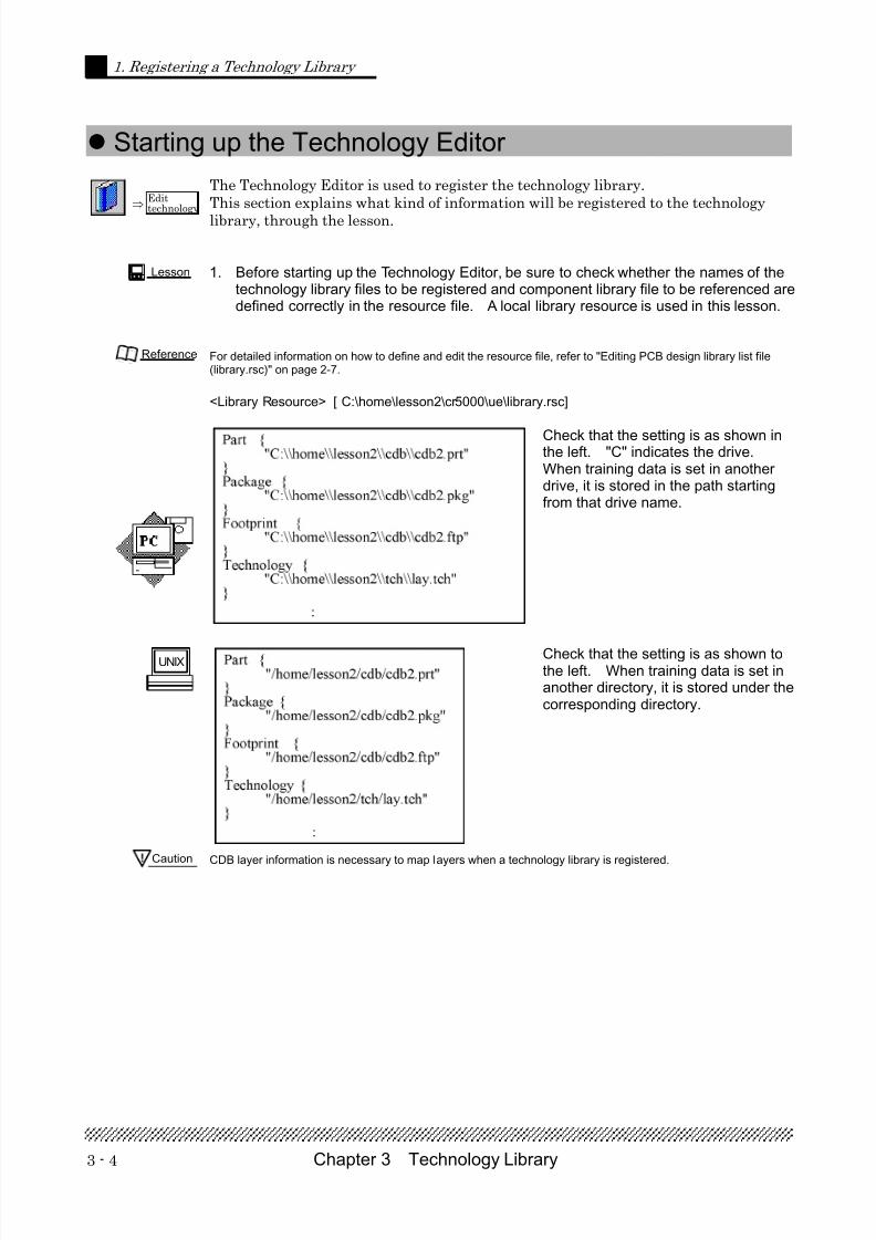
<Library Resource> [ C:\home\lesson2\cr5000\ue\library.rsc]
Check that the setting is as shown inthe left. "C" indicates the drive.When training data is set in anotherdrive, it is stored in the path startingfrom that drive name.
Check that the setting is as shown tothe left. When training data is set inanother directory, it is stored under thecorresponding directory.
CDB layer information is necessary to map layers when a technology library is registered.
Starting up the Technology Editor
Lesson
Reference
UNIX
Edittechnology⇒
Caution
7/27/2019 Design Library Master Training_cr
http://slidepdf.com/reader/full/design-library-master-trainingcr 24/89
3 - 5Chapter 3 Technology Library
1. Registering a Technology Library
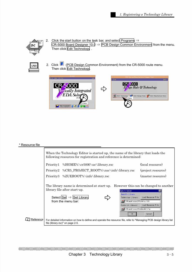
2. Click the start button on the task bar, and select Programs ⇒
CR-5000 Board Designer 10.0 ⇒ PCB Design Common Environment from the menu.
Then click Edit Technology .
2. Click (PCB Design Common Environment) from the CR-5000 route menu.
Then click Edit Technology.
* Resource file
When the Technology Editor is started up, the name of the library that loads thefollowing resources for registration and reference is determined:
Priority1 %HOME%\cr5000\ue\library.rsc (local resource)
Priority2 %CR5_PROJECT_ROOT%\zue\info\library.rsc (project resource)
Priority3 %ZUEROOT%\info\library.rsc (master resource)
The library name is determined at start-up. However this can be changed to another
library file after start-up.
Select Set ⇒ Set Library
from the menu bar:
For detailed information on how to define and operate the resource file, refer to "Managing PCB design library listfile (library.rsc)" on page 2-5.
Reference
Click
Click
UNIX
7/27/2019 Design Library Master Training_cr
http://slidepdf.com/reader/full/design-library-master-trainingcr 25/89
Chapter 3 Technology Library3 - 6
1. Registering a Technology Library
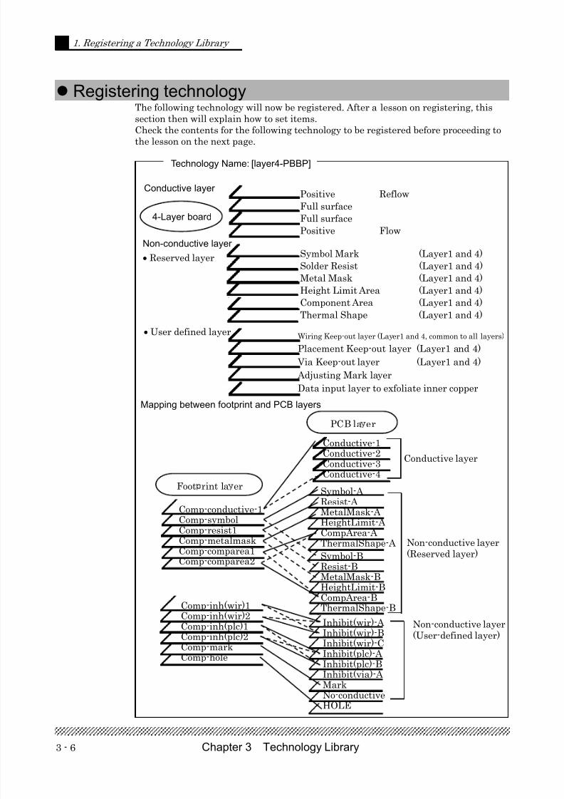
The following technology will now be registered. After a lesson on registering, thissection then will explain how to set items.Check the contents for the following technology to be registered before proceeding to
the lesson on the next page.
Registering technology
Technology Name: [layer4-PBBP]
Conductive layer
4-Layer board
Positive ReflowFull surfaceFull surfacePositive Flow
Non-conductive layer
• Reserved layer
• User defined layer
Symbol Mark (Layer1 and 4)Solder Resist (Layer1 and 4)
Metal Mask (Layer1 and 4)Height Limit Area (Layer1 and 4)Component Area (Layer1 and 4)Thermal Shape (Layer1 and 4)
Wiring Keep-out layer (Layer1 and 4, common to all layers)
Placement Keep-out layer (Layer1 and 4)
Via Keep-out layer (Layer1 and 4)
Adjusting Mark layer
Data input layer to exfoliate inner copper
Mapping between footprint and PCB layers
Foot rint la er
PCB la er
Comp-conductive-1Comp-symbolComp-resist1Comp-metalmaskComp-comparea1
Comp-comparea2
Comp-inh(wir)1Comp-inh(wir)2Comp-inh(plc)1Comp-inh(plc)2Comp-markComp-hole
Conductive-1Conductive-2Conductive-3Conductive-4
Symbol-AResist-AMetalMask-AHeightLimit-ACompArea-AThermalShape-A
Symbol-BResist-BMetalMask-BHeightLimit-BCompArea-BThermalShape-B
Inhibit(wir)-AInhibit(wir)-BInhibit(wir)-CInhibit(plc)-AInhibit(plc)-BInhibit(via)-AMark
No-conductiveHOLE
Conductive layer
Non-conductive layer(Reserved layer)
Non-conductive layer(User-defined layer)
7/27/2019 Design Library Master Training_cr
http://slidepdf.com/reader/full/design-library-master-trainingcr 26/89
3 - 7Chapter 3 Technology Library
1. Registering a Technology Library
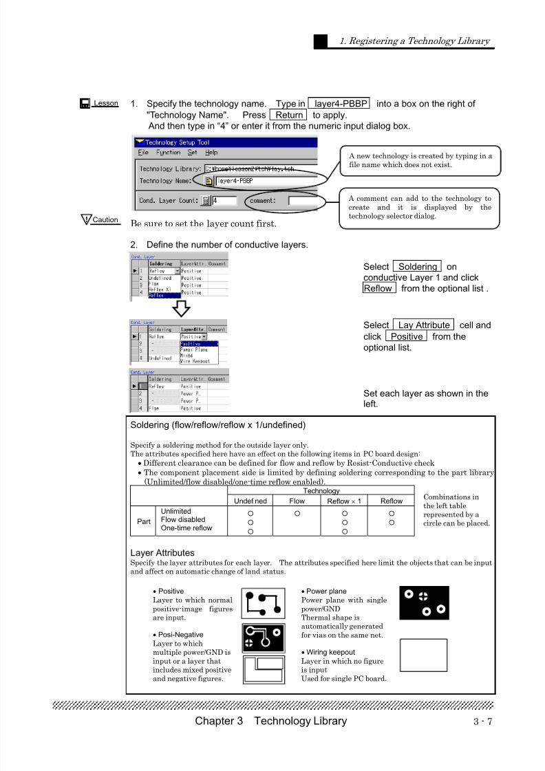
1. Specify the technology name. Type in layer4-PBBP into a box on the right of
"Technology Name". Press Return to apply.
And then type in “4” or enter it from the numeric input dialog box.
Be sure to set the layer count first.
2. Define the number of conductive layers.
Select Soldering onconductive Layer 1 and click
Reflow from the optional list .
Select Lay Attribute cell and
click Positive from the
optional list.
Set each layer as shown in the
left.
Soldering (flow/reflow/reflow x 1/undefined)
Specify a soldering method for the outside layer only.The attributes specified here have an effect on the following items in PC board design: • Different clearance can be defined for flow and reflow by Resist-Conductive check• The component placement side is limited by defining soldering corresponding to the part library
(Unlimited/flow disabled/one-time reflow enabled). Technology
Undefined Flow Reflow × 1 Reflow
Part
UnlimitedFlow disabledOne-time reflow
Layer AttributesSpecify the layer attributes for each layer. The attributes specified here limit the objects that can be inputand affect on automatic change of land status.
• Positive
Layer to which normalpositive-image figuresare input.
• Posi-Negative
Layer to whichmultiple power/GND isinput or a layer thatincludes mixed positive
and negative figures.
• Power plane
Power plane with singlepower/GNDThermal shape isautomatically generatedfor vias on the same net.
• Wiring keepout
Layer in which no figureis input
Used for single PC board.
Lesson
Combinations inthe left tablerepresented by acircle can be placed.
Caution
A new technology is created by typing in afile name which does not exist.
A comment can add to the technology tocreate and it is displayed by thetechnology selector dialog.
7/27/2019 Design Library Master Training_cr
http://slidepdf.com/reader/full/design-library-master-trainingcr 27/89
Chapter 3 Technology Library3 - 8
1. Registering a Technology Library
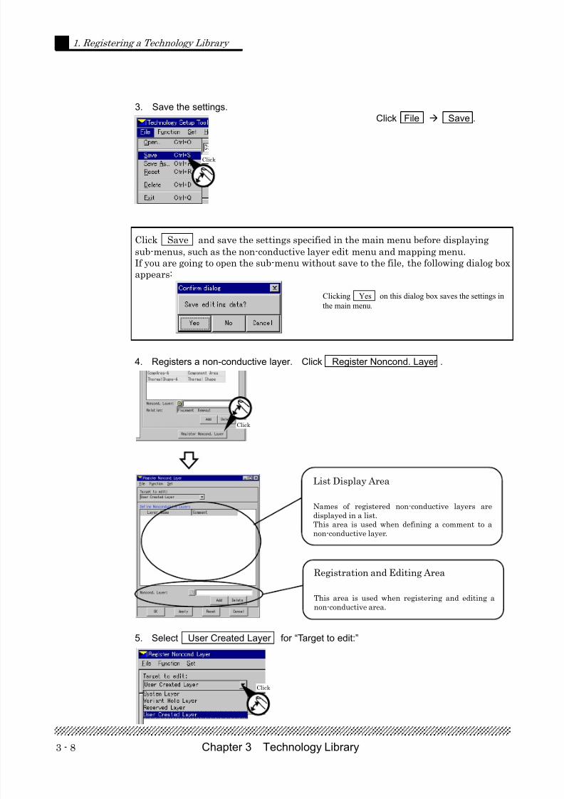
3. Save the settings.
Click File Save .
Click Save and save the settings specified in the main menu before displayingsub-menus, such as the non-conductive layer edit menu and mapping menu.If you are going to open the sub-menu without save to the file, the following dialog boxappears:
Clicking Yes on this dialog box saves the settings in
the main menu.
4. Registers a non-conductive layer. Click Register Noncond. Layer .
5. Select User Created Layer for “Target to edit:”
Click
Click
Registration and Editing Area
This area is used when registering and editing anon-conductive area.
List Display Area
Names of registered non-conductive layers aredisplayed in a list.This area is used when defining a comment to anon-conductive layer.
Click
7/27/2019 Design Library Master Training_cr
http://slidepdf.com/reader/full/design-library-master-trainingcr 28/89
3 - 9Chapter 3 Technology Library
1. Registering a Technology Library
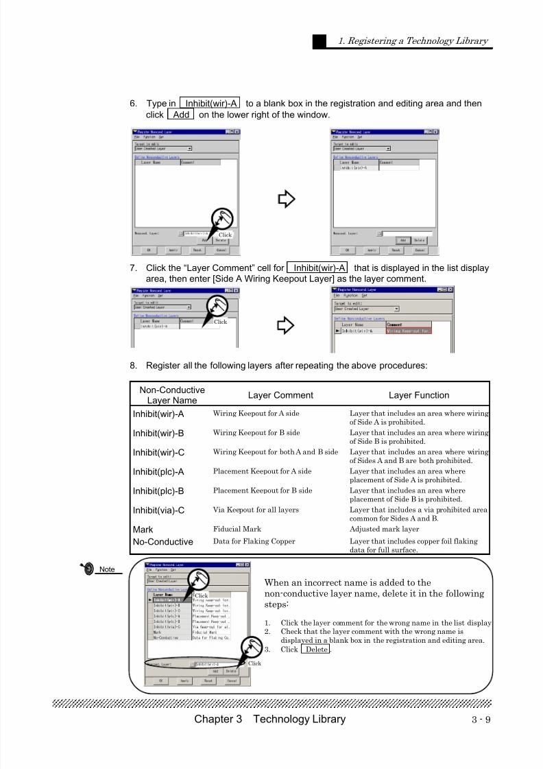
6. Type in Inhibit(wir)-A to a blank box in the registration and editing area and then
click Add on the lower right of the window.
7. Click the “Layer Comment” cell for Inhibit(wir)-A that is displayed in the list displayarea, then enter [Side A Wiring Keepout Layer] as the layer comment.
8. Register all the following layers after repeating the above procedures:
Non-Conductive
Layer Name
Layer Comment Layer Function
Inhibit(wir)-A Wiring Keepout for A side Layer that includes an area where wiringof Side A is prohibited.
Inhibit(wir)-B Wiring Keepout for B side Layer that includes an area where wiringof Side B is prohibited.
Inhibit(wir)-C Wiring Keepout for both A and B side Layer that includes an area where wiringof Sides A and B are both prohibited.
Inhibit(plc)-A Placement Keepout for A side Layer that includes an area whereplacement of Side A is prohibited.
Inhibit(plc)-B Placement Keepout for B side Layer that includes an area whereplacement of Side B is prohibited.
Inhibit(via)-C Via Keepout for all layers Layer that includes a via prohibited areacommon for Sides A and B.
Mark Fiducial Mark Adjusted mark layer
No-Conductive Data for Flaking Copper Layer that includes copper foil flakingdata for full surface.
When an incorrect name is added to thenon-conductive layer name, delete it in the followingsteps:
1. Click the layer comment for the wrong name in the list display2. Check that the layer comment with the wrong name is
displayed in a blank box in the registration and editing area.3. Click Delete .
Click
Note
Click
Click
Click
7/27/2019 Design Library Master Training_cr
http://slidepdf.com/reader/full/design-library-master-trainingcr 29/89
Chapter 3 Technology Library3 - 10
1. Registering a Technology Library
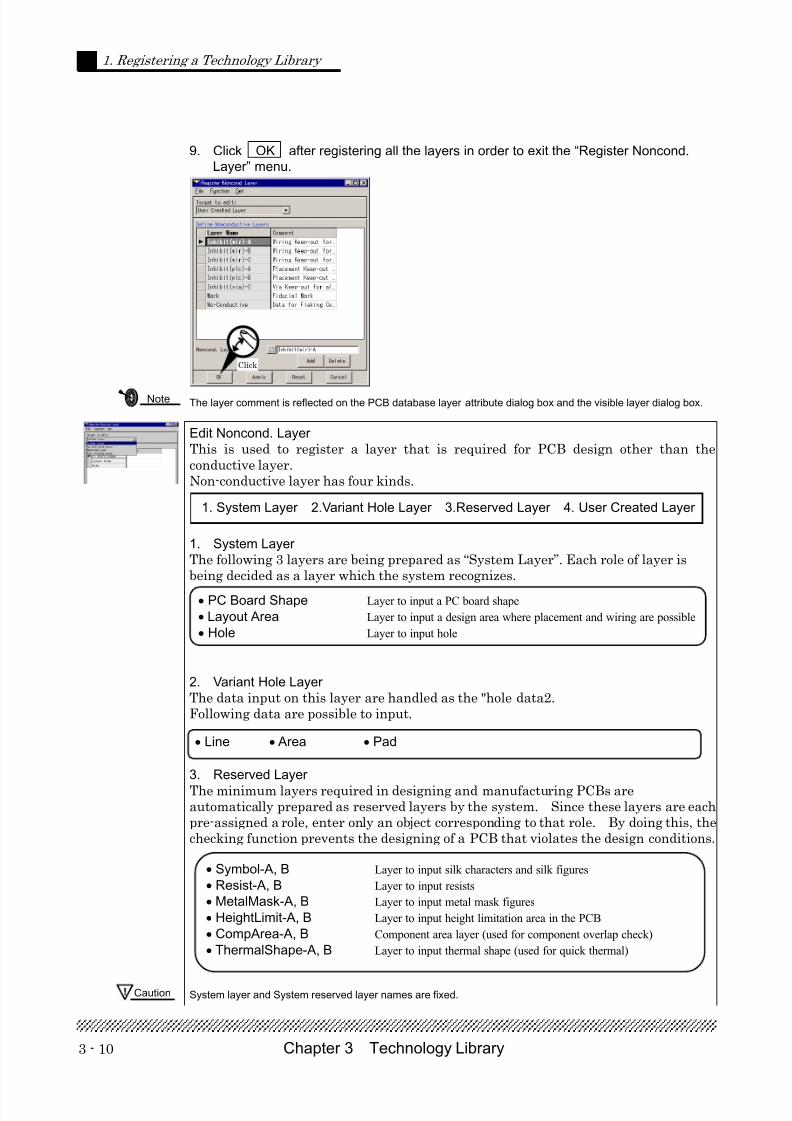
9. Click OK after registering all the layers in order to exit the “Register Noncond.
Layer” menu.
The layer comment is reflected on the PCB database layer attribute dialog box and the visible layer dialog box.
Edit Noncond. Layer
This is used to register a layer that is required for PCB design other than theconductive layer.Non-conductive layer has four kinds.
1. System Layer
The following 3 layers are being prepared as “System Layer”. Each role of layer isbeing decided as a layer which the system recognizes.
2. Variant Hole Layer
The data input on this layer are handled as the "hole data2.Following data are possible to input.
3. Reserved Layer
The minimum layers required in designing and manufacturing PCBs areautomatically prepared as reserved layers by the system. Since these layers are eachpre-assigned a role, enter only an object corresponding to that role. By doing this, thechecking function prevents the designing of a PCB that violates the design conditions.
System layer and System reserved layer names are fixed.
Note
Click
1. System Layer 2.Variant Hole Layer 3.Reserved Layer 4. User Created Layer
• Symbol-A, B Layer to input silk characters and silk figures
• Resist-A, B Layer to input resists
• MetalMask-A, B Layer to input metal mask figures
• HeightLimit-A, B Layer to input height limitation area in the PCB
• CompArea-A, B Component area layer (used for component overlap check)
• ThermalShape-A, B Layer to input thermal shape (used for quick thermal)
• PC Board Shape Layer to input a PC board shape
• Layout Area Layer to input a design area where placement and wiring are possible
• Hole Layer to input hole
• Line • Area • Pad
Caution
7/27/2019 Design Library Master Training_cr
http://slidepdf.com/reader/full/design-library-master-trainingcr 30/89
3 - 11Chapter 3 Technology Library
1. Registering a Technology Library
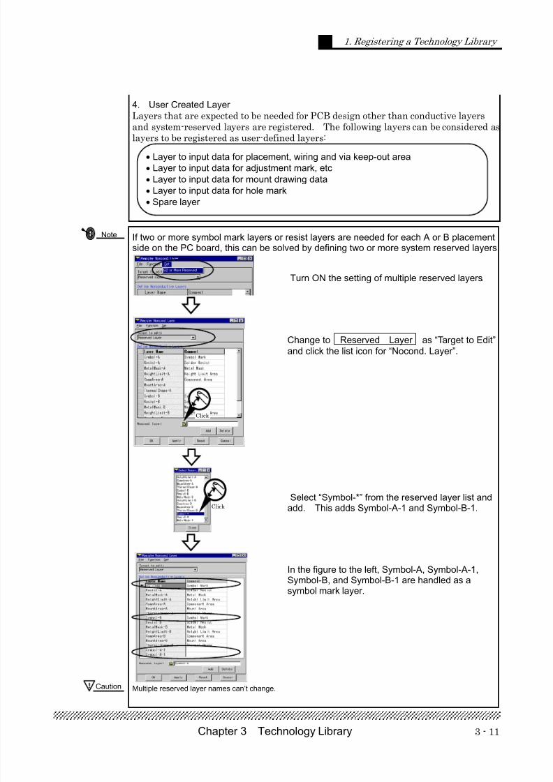
4. User Created Layer
Layers that are expected to be needed for PCB design other than conductive layersand system-reserved layers are registered. The following layers can be considered as
layers to be registered as user-defined layers:
If two or more symbol mark layers or resist layers are needed for each A or B placementside on the PC board, this can be solved by defining two or more system reserved layers.
Turn ON the setting of multiple reserved layers.
Change to Reserved Layer as “Target to Edit”
and click the list icon for “Nocond. Layer”.
Select “Symbol-*” from the reserved layer list andadd. This adds Symbol-A-1 and Symbol-B-1.
In the figure to the left, Symbol-A, Symbol-A-1,Symbol-B, and Symbol-B-1 are handled as asymbol mark layer.
Multiple reserved layer names can’t change.
Note
• Layer to input data for placement, wiring and via keep-out area
• Layer to input data for adjustment mark, etc
• Layer to input data for mount drawing data
• Layer to input data for hole mark
• Spare layer
Click
Caution
Click
7/27/2019 Design Library Master Training_cr
http://slidepdf.com/reader/full/design-library-master-trainingcr 31/89
Chapter 3 Technology Library3 - 12
1. Registering a Technology Library
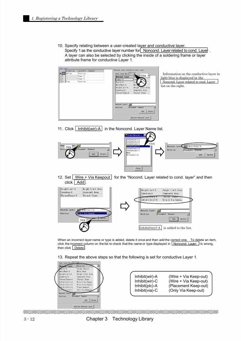
10. Specify relating between a user-created layer and conductive layer.
Specify 1 as the conductive layer number for Noncond. Layer related to cond. Layer .
A layer can also be selected by clicking the inside of a soldering frame or layer
attribute frame for conductive Layer 1.
Information on the conductive layer inlight blue is displayed in the
Noncond. Layer related to cond. Layerlist on the right.
11. Click Inhibit(wir)-A in the Noncond. Layer Name list.
12. Set Wire + Via Keepout for the “Nocond. Layer related to cond. layer” and thenclick Add .
When an incorrect layer name or type is added, delete it once and then add the correct one. To delete an item,click the incorrect column on the list to check that the name or type displayed in Noncond. Layer: is wrong,
then click Delete .
13. Repeat the above steps so that the following is set for conductive Layer 1.
Click
Inhibit(wir)-A is added to the list.
Click
Inhibit(wir)-A (Wire + Via Keep-out)Inhibit(wir)-C (Wire + Via Keep-out)Inhibit(plc)-A (Placement Keep-out)Inhibit(via)-C (Only Via Keep-out)
Click
Click
7/27/2019 Design Library Master Training_cr
http://slidepdf.com/reader/full/design-library-master-trainingcr 32/89
3 - 13Chapter 3 Technology Library
1. Registering a Technology Library
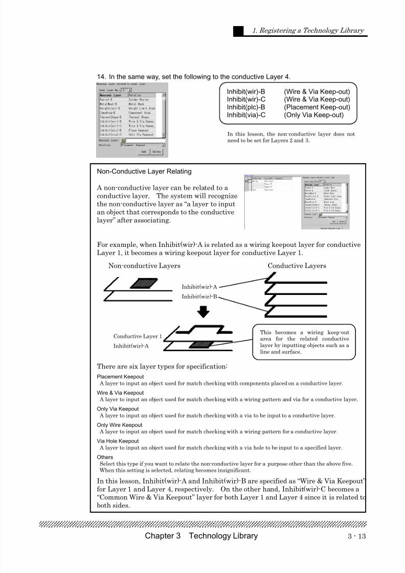
14. In the same way, set the following to the conductive Layer 4.
Non-Conductive Layer Relating
A non-conductive layer can be related to aconductive layer. The system will recognizethe non-conductive layer as “a layer to inputan object that corresponds to the conductivelayer” after associating.
For example, when Inhibit(wir)-A is related as a wiring keepout layer for conductiveLayer 1, it becomes a wiring keepout layer for conductive Layer 1.
There are six layer types for specification:
Placement Keepout
A layer to input an object used for match checking with components placed on a conductive layer.
Wire & Via Keepout
A layer to input an object used for match checking with a wiring pattern and via for a conductive layer.Only Via Keepout
A layer to input an object used for match checking with a via to be input to a conductive layer.
Only Wire Keepout
A layer to input an object used for match checking with a wiring pattern for a conductive layer.
Via Hole Keepout
A layer to input an object used for match checking with a via hole to be input to a specified layer.
Others
Select this type if you want to relate the non-conductive layer for a purpose other than the above five.When this setting is selected, relating becomes insignificant.
In this lesson, Inhibit(wir)-A and Inhibit(wir)-B are specified as “Wire & Via Keepout”for Layer 1 and Layer 4, respectively. On the other hand, Inhibit(wir)-C becomes a“Common Wire & Via Keepout” layer for both Layer 1 and Layer 4 since it is related toboth sides.
Inhibit(wir)-B (Wire & Via Keep-out)
Inhibit(wir)-C (Wire & Via Keep-out)Inhibit(plc)-B (Placement Keep-out)Inhibit(via)-C (Only Via Keep-out)
Non-conductive Layers Conductive Layers
Inhibit(wir)-A
Inhibit(wir)-B
Conductive Layer 1
Inhibit(wir)-A
This becomes a wiring keep-outarea for the related conductivelayer by inputting objects such as aline and surface.
In this lesson, the non-conductive layer does notneed to be set for Layers 2 and 3.
7/27/2019 Design Library Master Training_cr
http://slidepdf.com/reader/full/design-library-master-trainingcr 33/89
Chapter 3 Technology Library3 - 14
1. Registering a Technology Library
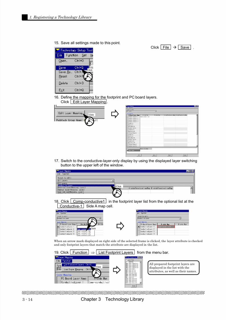
15. Save all settings made to this point.
Click File Save .
16. Define the mapping for the footprint and PC board layers.
Click Edit Layer Mapping .
17. Switch to the conductive-layer-only display by using the displayed layer switchingbutton to the upper left of the window.
18. Click Comp-conductive1 in the footprint layer list from the optional list at the
Conductive-1 Side A map cell.
When an arrow mark displayed on right side of the selected frame is clicked, the layer attribute is checkedand only footprint layers that match the attribute are displayed in the list.
19. Click Function ⇒ List Footprint Layers from the menu bar.
Click
Click
Click
Click
All prepared footprint layers aredisplayed in the list with theattributes, as well as their names.
Click
7/27/2019 Design Library Master Training_cr
http://slidepdf.com/reader/full/design-library-master-trainingcr 34/89
3 - 15Chapter 3 Technology Library
1. Registering a Technology Library
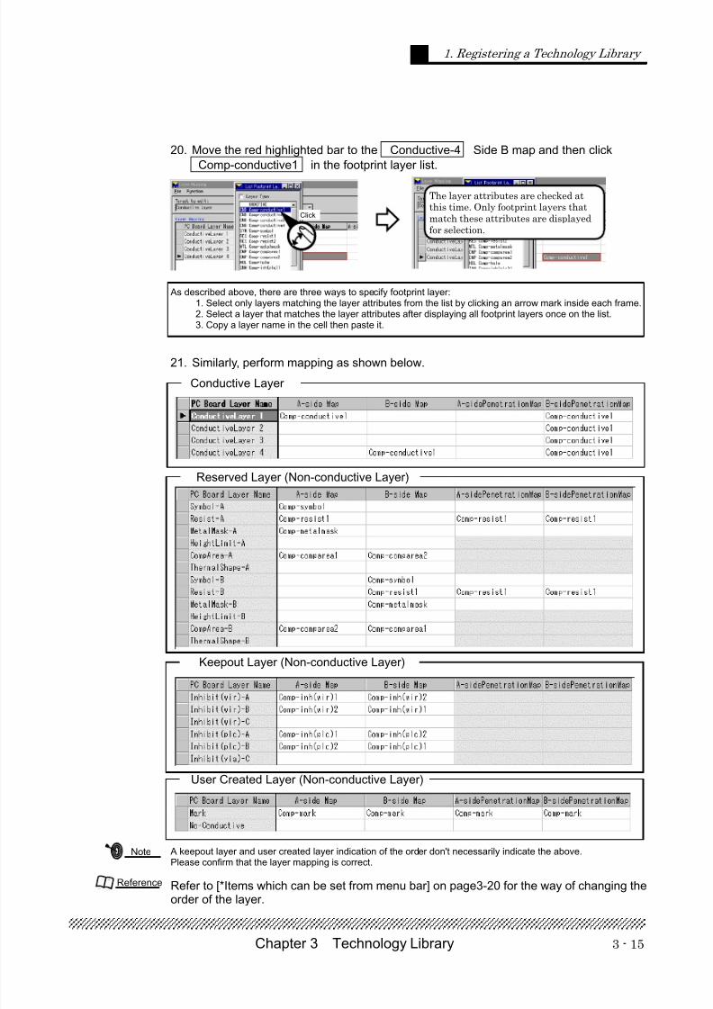
20. Move the red highlighted bar to the Conductive-4 Side B map and then click
Comp-conductive1 in the footprint layer list.
As described above, there are three ways to specify footprint layer:1. Select only layers matching the layer attributes from the list by clicking an arrow mark inside each frame.2. Select a layer that matches the layer attributes after displaying all footprint layers once on the list.3. Copy a layer name in the cell then paste it.
21. Similarly, perform mapping as shown below.
A keepout layer and user created layer indication of the order don't necessarily indicate the above.Please confirm that the layer mapping is correct.
Refer to [*Items which can be set from menu bar] on page3-20 for the way of changing theorder of the layer.
The layer attributes are checked atthis time. Only footprint layers thatmatch these attributes are displayedfor selection.
Click
Reserved Layer (Non-conductive Layer)
Conductive Layer
Keepout Layer (Non-conductive Layer)
User Created Layer (Non-conductive Layer)
Reference
Note
7/27/2019 Design Library Master Training_cr
http://slidepdf.com/reader/full/design-library-master-trainingcr 35/89
Chapter 3 Technology Library3 - 16
1. Registering a Technology Library
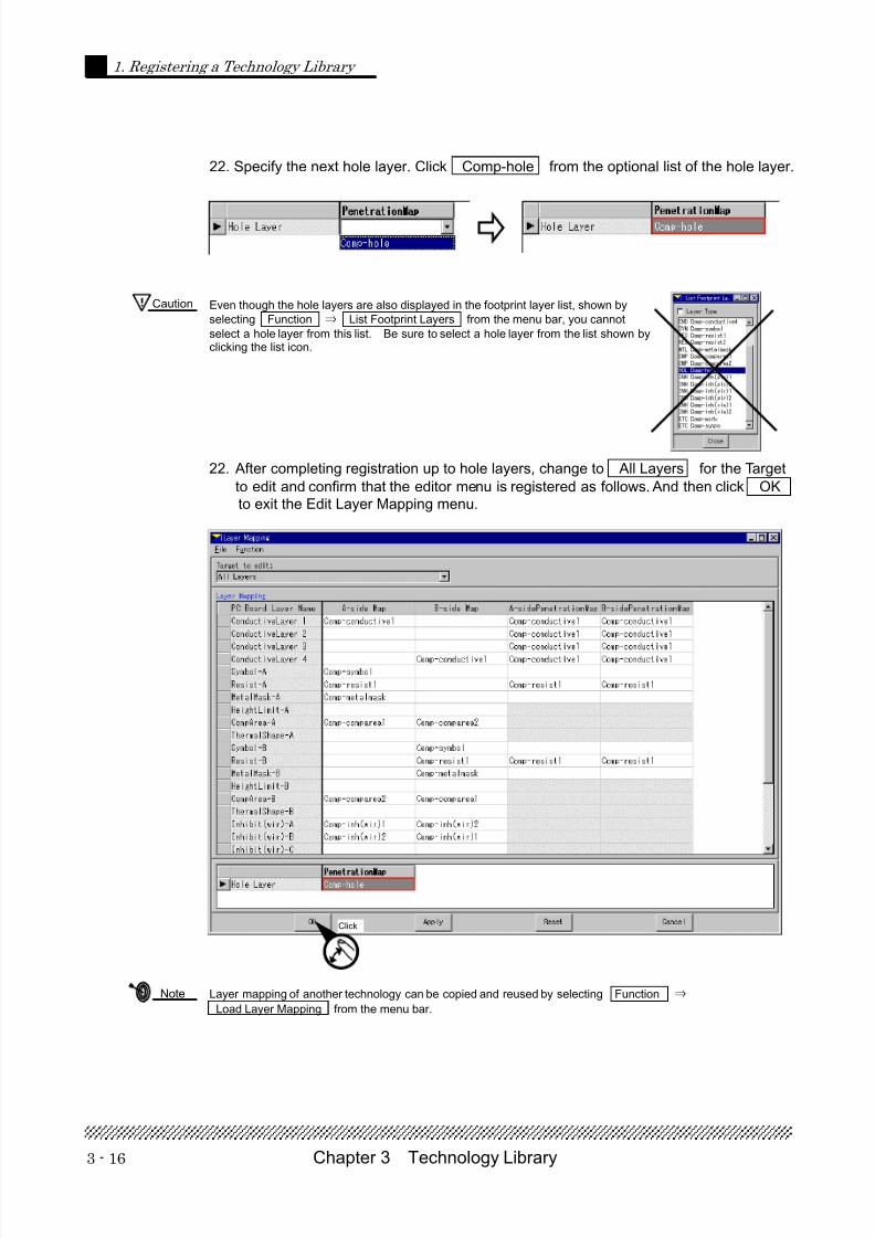
22. Specify the next hole layer. Click Comp-hole from the optional list of the hole layer.
Even though the hole layers are also displayed in the footprint layer list, shown by
selecting Function ⇒ List Footprint Layers from the menu bar, you cannot
select a hole layer from this list. Be sure to select a hole layer from the list shown byclicking the list icon.
22. After completing registration up to hole layers, change to All Layers for the Target
to edit and confirm that the editor menu is registered as follows. And then click OK
to exit the Edit Layer Mapping menu.
Layer mapping of another technology can be copied and reused by selecting Function ⇒
Load Layer Mapping from the menu bar.
Note
Caution
Click
7/27/2019 Design Library Master Training_cr
http://slidepdf.com/reader/full/design-library-master-trainingcr 36/89
3 - 17Chapter 3 Technology Library
1. Registering a Technology Library
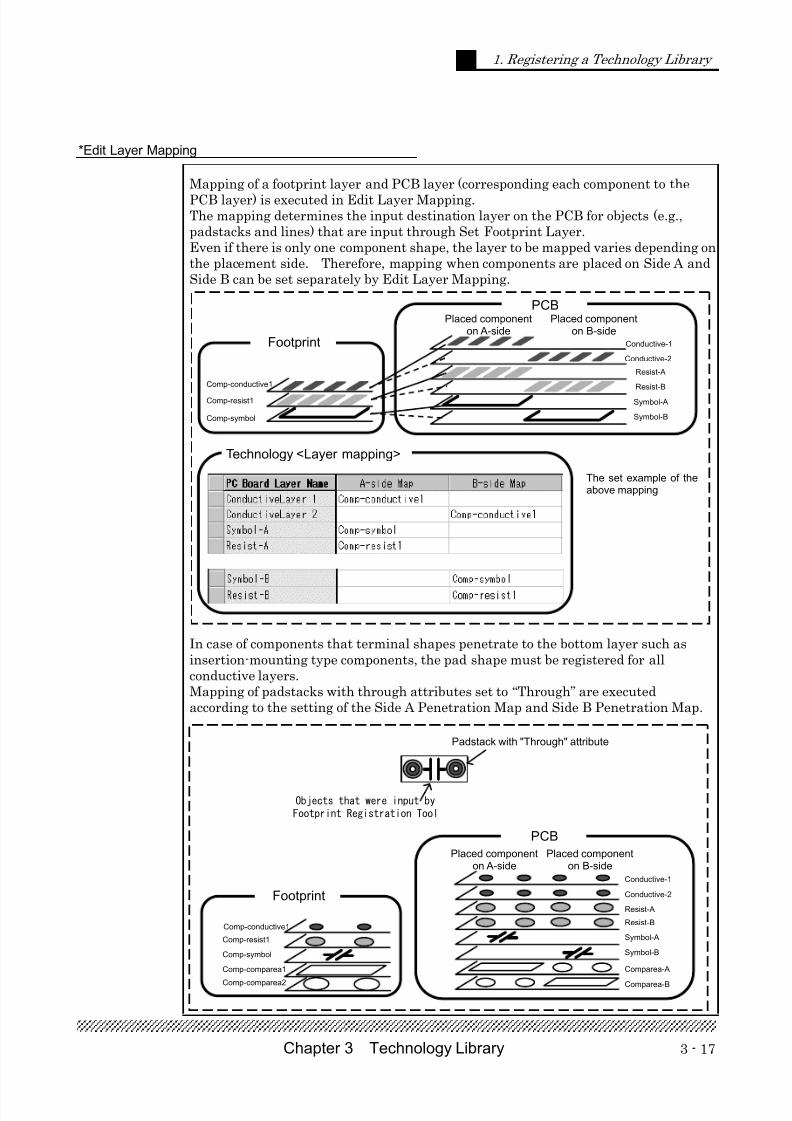
*Edit Layer Mapping
Mapping of a footprint layer and PCB layer (corresponding each component to the
PCB layer) is executed in Edit Layer Mapping.The mapping determines the input destination layer on the PCB for objects (e.g.,padstacks and lines) that are input through Set Footprint Layer.Even if there is only one component shape, the layer to be mapped varies depending onthe placement side. Therefore, mapping when components are placed on Side A andSide B can be set separately by Edit Layer Mapping.
Comp-conductive1
Comp-resist1
Comp-symbol
Conductive-1
Conductive-2
Resist-A
Resist-B
Symbol-A
Symbol-B
In case of components that terminal shapes penetrate to the bottom layer such asinsertion-mounting type components, the pad shape must be registered for allconductive layers.Mapping of padstacks with through attributes set to “Through” are executedaccording to the setting of the Side A Penetration Map and Side B Penetration Map.
Padstack with "Through" attribute
Objects that were input by
Footprint Registration Tool
Comp-conductive1
Comp-resist1
Comp-symbol
Comp-comparea1
Comp-comparea2
Conductive-1
Conductive-2
Resist-A
Resist-B
Symbol-A
Symbol-B
Comparea-A
Comparea-B
The set example of theabove mapping
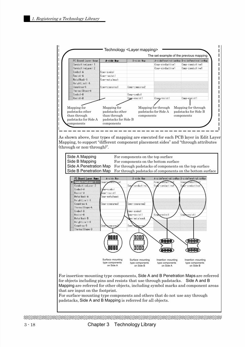
Technology <Layer mapping>
Footprint
PCBPlaced component
on A-sidePlaced component
on B-side
PCB
Placed componenton A-side
Placed componenton B-side
Footprint
7/27/2019 Design Library Master Training_cr
http://slidepdf.com/reader/full/design-library-master-trainingcr 37/89
Chapter 3 Technology Library3 - 18
1. Registering a Technology Library
As shown above, four types of mapping are executed for each PCB layer in Edit LayerMapping, to support “different component placement sides” and “through attributes(through or non-through)”.
Side A Mapping For components on the top surface Side B Mapping For components on the bottom surface Side A Penetration Map For through padstacks of components on the top surface Side B Penetration Map For through padstacks of components on the bottom surface
For insertion-mounting type components, Side A and B Penetration Maps are referredfor objects including pins and resists that use through padstacks. Side A and B
Mapping are referred for other objects, including symbol marks and component areasthat are input on the footprint.For surface-mounting type components and others that do not use any throughpadstacks, Side A and B Mapping is referred for all objects.
Mapping forpadstacks otherthan throughpadstacks for Side Acomponents
Mapping forpadstacks otherthan throughpadstacks for Side Bcomponents
Mapping for throughpadstacks for Side Acomponents
Mapping for throughpadstacks for Side Bcomponents
Technology <Layer mapping>
The set example of the previous mapping
type componentson Side A
type componentson Side B
type componentson Side A
type componentson Side B
Surface - mounting Surface - mounting Insertion - mounting Insertion - mounting
7/27/2019 Design Library Master Training_cr
http://slidepdf.com/reader/full/design-library-master-trainingcr 38/89
3 - 19Chapter 3 Technology Library
1. Registering a Technology Library
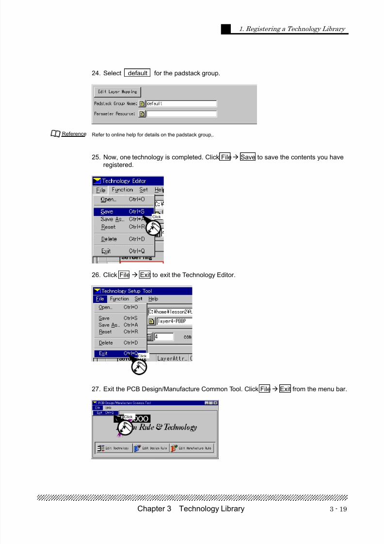
24. Select default for the padstack group.
Refer to online help for details on the padstack group,.
25. Now, one technology is completed. Click File Save to save the contents you have
registered.
26. Click File Exit to exit the Technology Editor.
27. Exit the PCB Design/Manufacture Common Tool. Click File Exit from the menu bar.
Click
Reference
Click
Click
7/27/2019 Design Library Master Training_cr
http://slidepdf.com/reader/full/design-library-master-trainingcr 39/89
Chapter 3 Technology Library3 - 20
1. Registering a Technology Library
* Items which can be set from menu bar
It describes items which can be set by the Set of the menu bar in Technology Editor.
1. Specifying the display order of layer name.
Set Change Order of Layer Name…
The display order of the layer name is changedon dialog where it started.
2. Using the RulesbyArea Layer.
Set RulesByArea
The RulesByArea can specify special rule (e.g. Design Rule Stack name, WiringWidth Stack name for an area and Default Padstack name) and the area is input bythe specified rule. When the RulesByArea is set to "ON" in the Technology editor andthen the Board Generation tool is performed, the layer that name is [RulesByArea] isadded to the PCB data and the area which specified special rules can be created onthe PCB.
If you want to set the RulesByArea layer to an existing PCB data, you need to update the technology specifiedby the PCB Technology Update tool to reflect it to the PCB data after “RulesByArea” was specified.
For details of the operations which RulesByArea are used for, refer to [Master Training <EngineeringChange/Operation].
1. The display order of layers can be specified.
2. The special rule for area can be specified.3. The sub-layer for connecting between conductive
data can be specified.4. This item is used by HIC design. HIC is an optional
module.
The line which selected is changed toup or down and then the display orderis changed.
Caution
Reference
PCB databaseDesign Rule A
Design Rule BRulesByAre
7/27/2019 Design Library Master Training_cr
http://slidepdf.com/reader/full/design-library-master-trainingcr 40/89
3 - 21Chapter 3 Technology Library
1. Registering a Technology Library
3. Using Sub-conductive layers.
Set
Sub Cond. Layers
The Sub-conductive layer is the layer which the data to connect a different net such astie point are input to. Some different nets in the schematic are connected on the tiepoint but their nets are handled as same net on PCB design. Board Designer can'tconnect between different nets. So the Sub-conductive layer is used. When the datawas input to the Sub-conductive layer, they can be output as same net by the PatternConnection Pinlist Output program (bdnetout).When the Sub Cond. Layers is set to "ON" in the Technology editor and then the BoardGeneration tool is performed, layers names are [Subconductive-1] and
[Subconductive-2] etc are added with specified conductive count to the PCB.
If you want to set the Sub-conductive layer to a existing PCB data, you need to update the technology specifiedby the PCB Technology Update tool to reflect it to the PCB data after Sub Cond. Layers” was specified.
Refer to online help [Batch Program Help] for details of “Pattern Connection Pinlist Output”.
4. Using Sub Dielectric layers.
Set Set Dielectric Area…
The dielectric area layer is used when a cross glass of the “Embedded ComponentDesign Module (HIC)” is generated.The “Embedded Component Design Module” is optional module.
Specify the count of dielectric layers on the dialogwhere it started.
Refer to the online help for details of “Embedded Component Design Module”.
Conductive-1(Conductive Layer)
SubConductive-1(Sub Layer – Non-conductive Layer)
Conductive-2(Conductive Layer)
SubConductive-2(Sub Layer – Non-conductive Layer)
Reference
Caution
Click
Reference
7/27/2019 Design Library Master Training_cr
http://slidepdf.com/reader/full/design-library-master-trainingcr 41/89
3 - 22
2. Operating the Technology Library
Chapter 3 Technology Library
This section explains the setting items for the Technology Library that you have upuntil now only seen. In order to deepen your knowledge, this section offers
instructions on how to actually operate the Technology Library.
Specifications According to Destination A component shape may change according to the destination.But in case of that the destination component can be used properly with one footprintby layer mapping.
When a silk shape changes according to the destination:
Company A
Company B
When a component shape changes depending on the board density:
Low-density
High-density
As shown above, even when mounting the same components, the shape may requiredelicate changes.
If you try to support such changes by separately registering each on a footprint, thenumber of components becomes too large and the configuration of the CDB librarycannot be utilized fully.
Therefore, it is best to group the same components and manage them in one footprint,and to handle the differences in component shape depending on destination by using atechnology library.
The following introduces “Change in Specifications by Mapping” as a handlingmethod.
7/27/2019 Design Library Master Training_cr
http://slidepdf.com/reader/full/design-library-master-trainingcr 42/89
3 - 23Chapter 3 Technology Library
2. Operating the Technology Library
Change of Specification by Mapping
Specifications can be changed to support most destinations by mapping the footprint
layer and the PCB layer.
For example, when a silk shape is different between Companies A and B;
Conductive layer
for A-side
Conductive layer
for B-side
Symbol mark layer
for Company A
Conductive layer
for A-side
Conductive
(Terminal)
Symbol mark for Company A
Symbol mark for Company B
Technology for Company A
Technology for Company B
Conductive layer
for B-side
Symbol mark layer
for Company B
Prepare “Symbol mark layer for Company A” and “Symbol mark layer for Company B”in the footprint layer in advance, and input each symbol mark into the correspondinglayer. Then, create a technology mapping for Company A and one for Company B by
using the technology library.
This method can support differences in high or low board density.
Conductive for High-density(Terminal)
Conductive for Low-density(Terminal)
Symbol mark
Technology for High-density
Technology for Low-density
Conductive layer
for A-side
Conductive layer for B-side
Symbol mark layer
Conductive layer
for A-side
Conductive layer for B-side
Symbol mark layer
Caution must be taken, however, since the number of footprint layers to be preparedwill increase and the mapping operation may become complex when you use mappingto solve all such support.
7/27/2019 Design Library Master Training_cr
http://slidepdf.com/reader/full/design-library-master-trainingcr 43/89
Chapter 3 Technology Library3 - 24
2. Operating the Technology Library
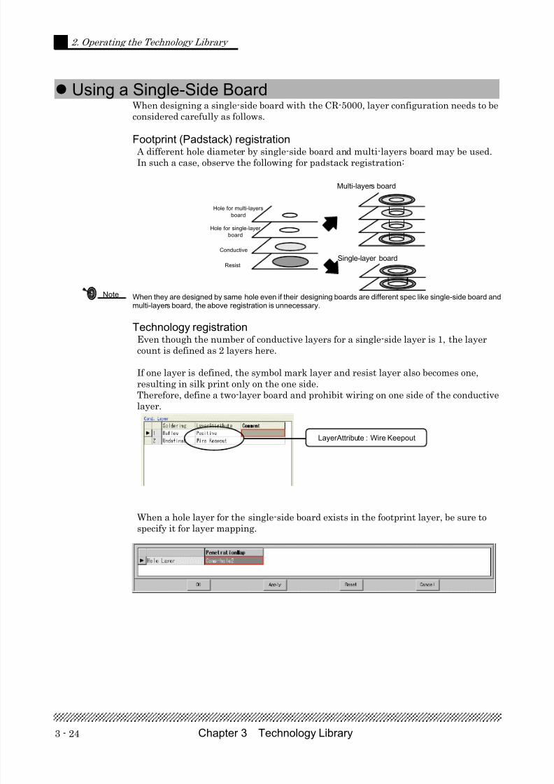
When designing a single-side board with the CR-5000, layer configuration needs to beconsidered carefully as follows.
Footprint (Padstack) registration A different hole diameter by single-side board and multi-layers board may be used.In such a case, observe the following for padstack registration:
Hole for multi-layers
board
Hole for single-layer
board
Conductive
Resist
Multi-layers board
Single-layer board
When they are designed by same hole even if their designing boards are different spec like single-side board andmulti-layers board, the above registration is unnecessary.
Technology registrationEven though the number of conductive layers for a single-side layer is 1, the layercount is defined as 2 layers here.
If one layer is defined, the symbol mark layer and resist layer also becomes one,resulting in silk print only on the one side.Therefore, define a two-layer board and prohibit wiring on one side of the conductivelayer.
When a hole layer for the single-side board exists in the footprint layer, be sure tospecify it for layer mapping.
Using a Single-Side Board
Note
LayerAttribute : Wire Keepout
7/27/2019 Design Library Master Training_cr
http://slidepdf.com/reader/full/design-library-master-trainingcr 44/89
3 - 25Chapter 3 Technology Library
2. Operating the Technology Library
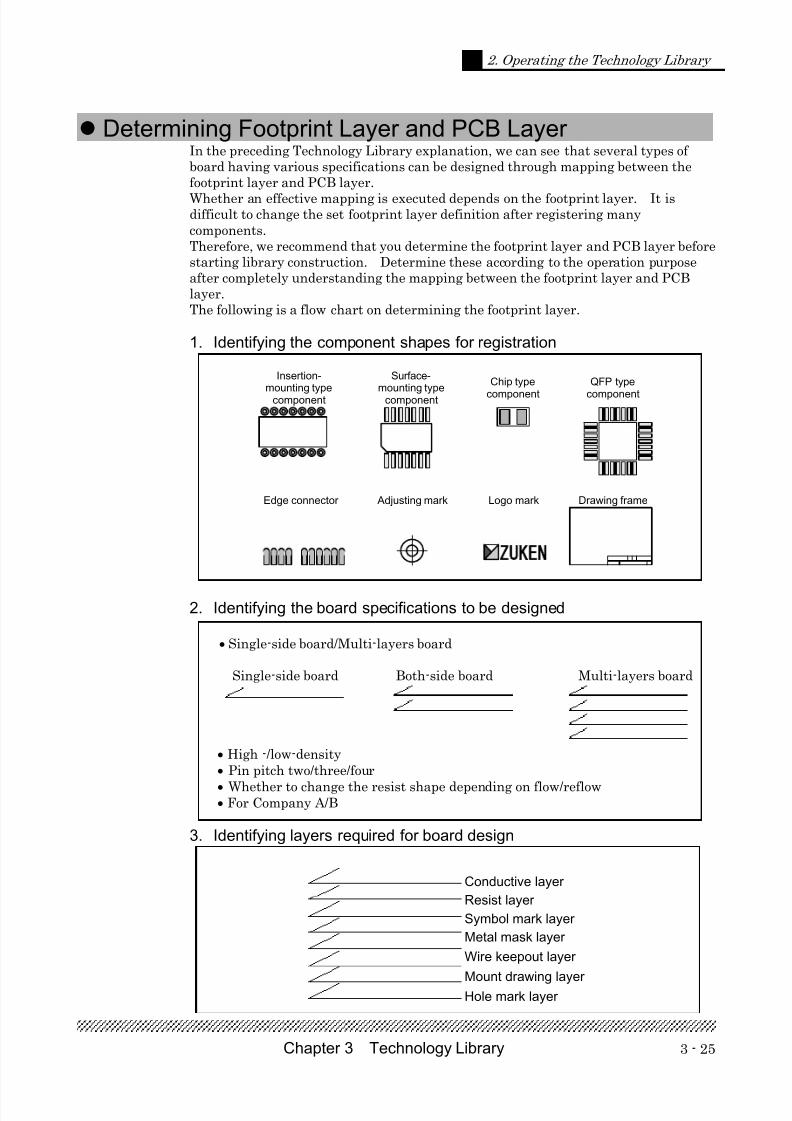
In the preceding Technology Library explanation, we can see that several types ofboard having various specifications can be designed through mapping between thefootprint layer and PCB layer.
Whether an effective mapping is executed depends on the footprint layer. It isdifficult to change the set footprint layer definition after registering manycomponents.Therefore, we recommend that you determine the footprint layer and PCB layer beforestarting library construction. Determine these according to the operation purposeafter completely understanding the mapping between the footprint layer and PCBlayer.The following is a flow chart on determining the footprint layer.
1. Identifying the component shapes for registration
Insertion-
mounting typecomponent
Surface-
mounting typecomponent
Chip type
component
QFP type
component
Edge connector Adjusting mark Logo mark Drawing frame
ZU N
2. Identifying the board specifications to be designed
• Single-side board/Multi-layers board
Single-side board Both-side board Multi-layers board
• High -/low-density• Pin pitch two/three/four
• Whether to change the resist shape depending on flow/reflow• For Company A/B
3. Identifying layers required for board design
Determining Footprint Layer and PCB Layer
Conductive layer
Resist layer
Symbol mark layer
Metal mask layer
Wire keepout layer
Mount drawing layerHole mark layer
7/27/2019 Design Library Master Training_cr
http://slidepdf.com/reader/full/design-library-master-trainingcr 45/89
Chapter 3 Technology Library3 - 26
2. Operating the Technology Library
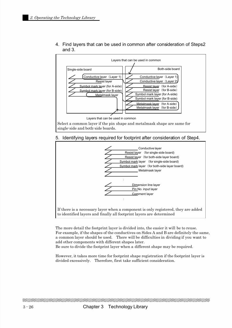
4. Find layers that can be used in common after consideration of Steps2and 3.
Conductive layer (Layer 1)
Resist layer
Metalmask layer
Symbol mark layer (for A-side) Resist layer (for A-side)
Metalmask layer (for A-side)
Single-side board Both-side board
Layers that can be used in common
Conductive layer (Layer 1)
Conductive layer (Layer 2)
Resist layer (for B-side)Symbol mark layer (for B-side)Symbol mark layer (for A-side)
Symbol mark layer (for B-side)
Metalmask layer (for B-side)
Layers that can be used in common Select a common layer if the pin shape and metalmask shape are same forsingle-side and both-side boards.
5. Identifying layers required for footprint after consideration of Step4.
Conductive layer
Resist layer (for single-side board)
Metalmask layer
Resist layer (for both-side layer board)
:
Symbol mark layer (for single-side board)
Symbol mark layer (for both-side layer board)
Dimension line layer
Comment layer
Pin No. input layer
:
If there is a necessary layer when a component is only registered, they are addedto identified layers and finally all footprint layers are determined
The more detail the footprint layer is divided into, the easier it will be to reuse.For example, if the shapes of the conductives on Sides A and B are definitely the same,a common layer should be used. There will be difficulties in dividing if you want toadd other components with different shapes later.Be sure to divide the footprint layer when a different shape may be required.
However, it takes more time for footprint shape registration if the footprint layer isdivided excessively. Therefore, first take sufficient consideration.
7/27/2019 Design Library Master Training_cr
http://slidepdf.com/reader/full/design-library-master-trainingcr 46/89
7/27/2019 Design Library Master Training_cr
http://slidepdf.com/reader/full/design-library-master-trainingcr 47/89
4 - 1
1. Registering a Design Rule Library
Chapter 4 Design Rule Library
The Design Rule LibraryThe design rule library (RUL) registers general rules for PC board design.
• Clearance values
• Pattern width
• Via used in wiring
• Grid
A new PC board is generated by specifying design rules from the design rule librarythat are most similar to the PC board specifications. General design rules are then
duplicated to generate a design rule database (RUL).
Detailed specifications belonging to each PC board (e.g., pattern width for each netname) are defined in a design rule database using another tool.
Refer to [Master Training <PCB Design>] for details on design rules specific to PCB.
The design rule library is designed to have several design rules according to thenumber of PC board layers and setting values. Each design rule configures a file.
TCH SpecificationA
Technology library
PC Board Database Design Rule Database
Board Generation
PCB RUL
Design rule library
General design rules
Design rules specificto the PC board
SpecificationB
SpecificationC
Example
Reference
Directory for Design Rules
A.rul B.rul C.rul D.rul
Design rule library specifies thedirectory name in the library.rsc file.
7/27/2019 Design Library Master Training_cr
http://slidepdf.com/reader/full/design-library-master-trainingcr 48/89
Chapter 4 Design Rule Library4 - 2
1. Registering a Design Rule Library
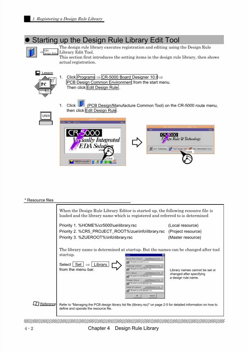
The design rule library executes registration and editing using the Design RuleLibrary Edit Tool.This section first introduces the setting items in the design rule library, then shows
actual registration.
1. Click Programs ⇒ CR-5000 Board Designer 10.0 ⇒
PCB Design Common Environment from the start menu.
Then click Edit Design Rule .
1. Click (PCB Design/Manufacture Common Tool) on the CR-5000 route menu,
then click Edit Design Rule.
* Resource files
When the Design Rule Library Editor is started up, the following resource file isloaded and the library name which is registered and referred to is determined
Priority 1. %HOME%\cr5000\ue\library.rsc (Local resource)
Priority 2. %CR5_PROJECT_ROOT%\zue\info\library.rsc (Project resource)
Priority 3. %ZUEROOT%\info\library.rsc (Master resource)
The library name is determined at startup. But the names can be changed after toolstartup.
Select Set ⇒ Library
from the menu bar.
Refer to "Managing the PCB design library list file (library.rsc)" on page 2-5 for detailed information on how to
define and operate the resource file.
Starting up the Design Rule Library Edit Tool
EditDesign Rules
⇒
Library names cannot be set or changed after specifyinga design rule name.
Reference
UNIX
Click
Click
Lesson
7/27/2019 Design Library Master Training_cr
http://slidepdf.com/reader/full/design-library-master-trainingcr 49/89
4 - 3Chapter 4 Design Rule Library
1. Registering a Design Rule Library
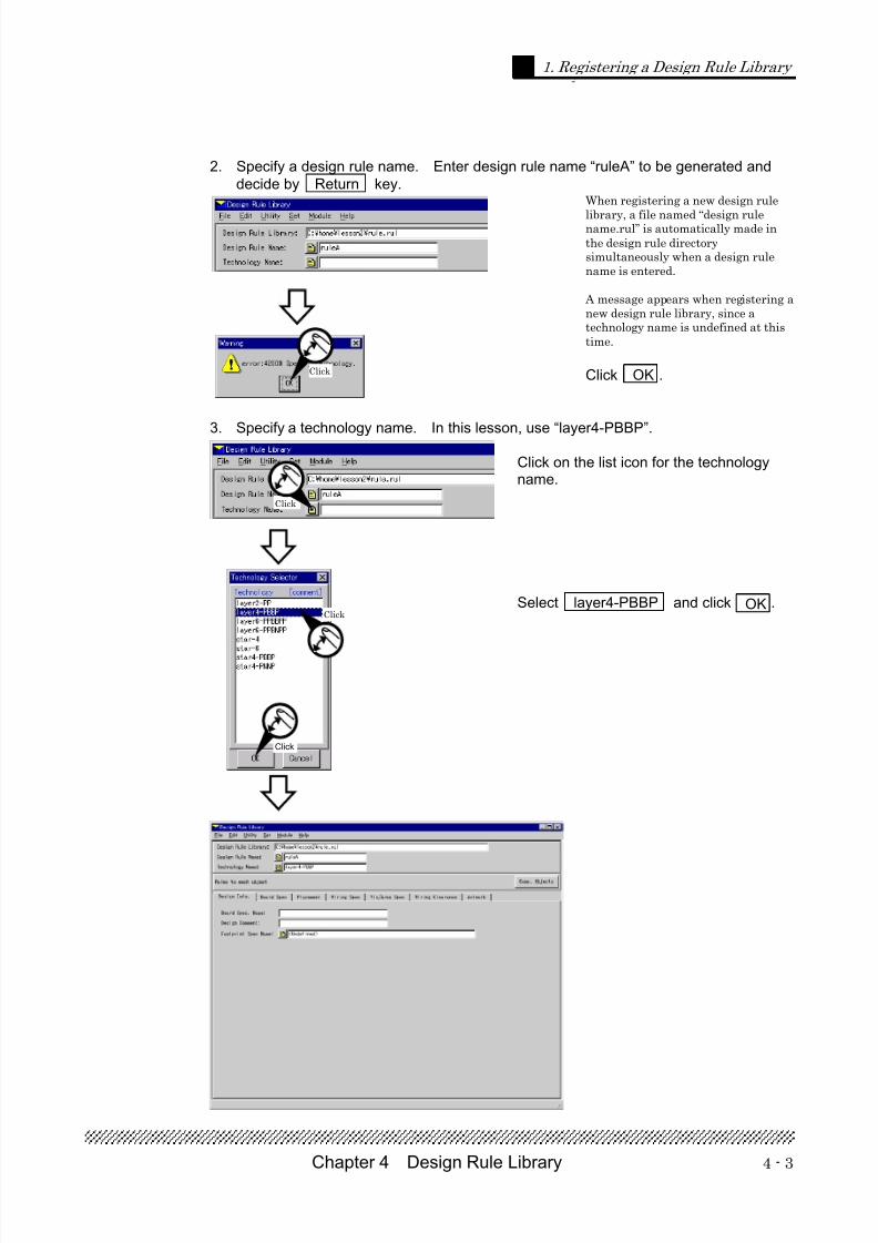
2. Specify a design rule name. Enter design rule name “ruleA” to be generated and
decide by Return key.When registering a new design rule
library, a file named “design rulename.rul” is automatically made inthe design rule directorysimultaneously when a design rulename is entered.
A message appears when registering anew design rule library, since atechnology name is undefined at thistime.
Click OK .
3. Specify a technology name. In this lesson, use “layer4-PBBP”.
Click on the list icon for the technologyname.
Select layer4-PBBP and click OK .
Click
Click
Click
Click
7/27/2019 Design Library Master Training_cr
http://slidepdf.com/reader/full/design-library-master-trainingcr 50/89
Chapter 4 Design Rule Library4 - 4
1. Registering a Design Rule Library
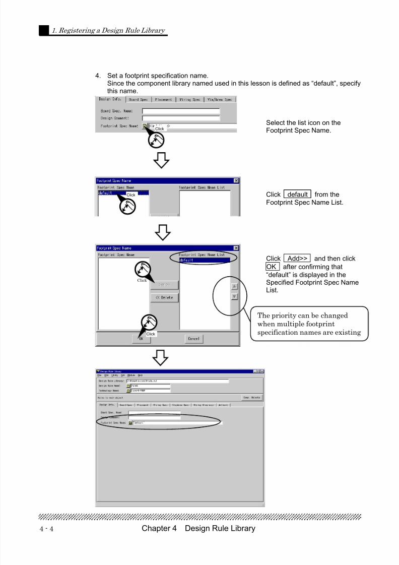
4. Set a footprint specification name.Since the component library named used in this lesson is defined as “default”, specifythis name.
Select the list icon on theFootprint Spec Name.
Click default from theFootprint Spec Name List.
Click Add>> and then click
OK after confirming that
“default” is displayed in theSpecified Footprint Spec NameList.
Click
Click
The priority can be changedwhen multiple footprintspecification names are existing
Click
Click
7/27/2019 Design Library Master Training_cr
http://slidepdf.com/reader/full/design-library-master-trainingcr 51/89
4 - 5Chapter 4 Design Rule Library
1. Registering a Design Rule Library
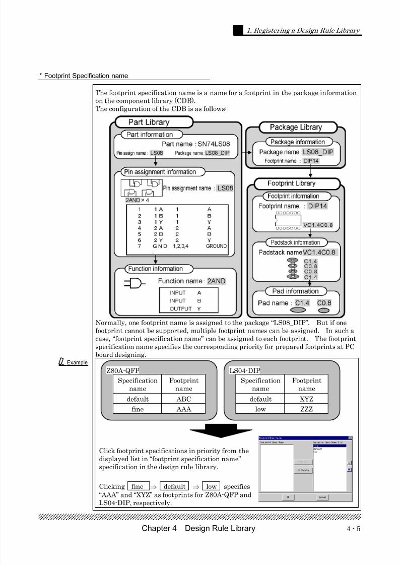
* Footprint Specification name
The footprint specification name is a name for a footprint in the package information
on the component library (CDB).The configuration of the CDB is as follows:
Normally, one footprint name is assigned to the package “LS08_DIP”. But if onefootprint cannot be supported, multiple footprint names can be assigned. In such acase, “footprint specification name” can be assigned to each footprint. The footprintspecification name specifies the corresponding priority for prepared footprints at PCboard designing.
Click footprint specifications in priority from thedisplayed list in “footprint specification name”specification in the design rule library.
Clicking fine ⇒ default ⇒ low specifies
“AAA” and “XYZ” as footprints for Z80A-QFP andLS04-DIP, respectively.
Z80A-QFP
Specificationname
Footprintname
default ABC
fine AAA
LS04-DIP
Specificationname
Footprintname
default XYZ
low ZZZ
Example
7/27/2019 Design Library Master Training_cr
http://slidepdf.com/reader/full/design-library-master-trainingcr 52/89
Chapter 4 Design Rule Library4 - 6
1. Registering a Design Rule Library
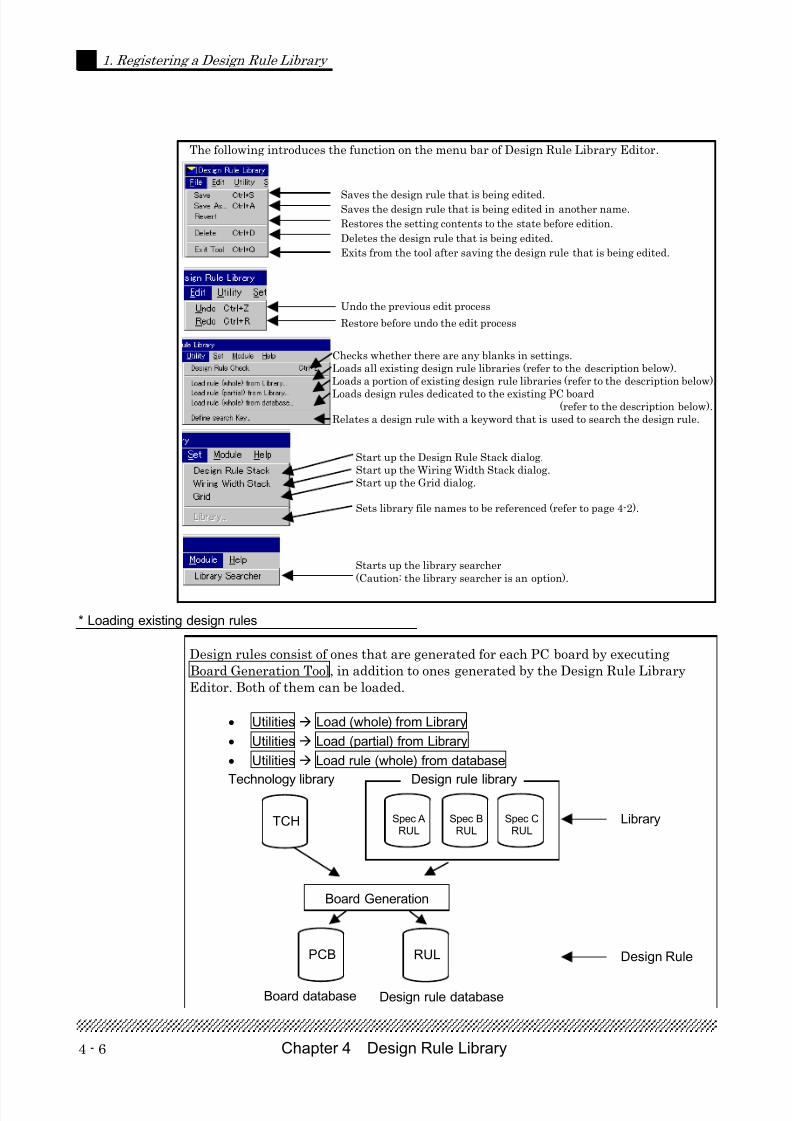
The following introduces the function on the menu bar of Design Rule Library Editor.
Saves the design rule that is being edited.Saves the design rule that is being edited in another name.
Restores the setting contents to the state before edition.
Deletes the design rule that is being edited.
Exits from the tool after saving the design rule that is being edited.
Undo the previous edit process
Restore before undo the edit process
Checks whether there are any blanks in settings.Loads all existing design rule libraries (refer to the description below).Loads a portion of existing design rule libraries (refer to the description below).
Loads design rules dedicated to the existing PC board(refer to the description below).
Relates a design rule with a keyword that is used to search the design rule.
Start up the Design Rule Stack dialog.Start up the Wiring Width Stack dialog.Start up the Grid dialog.
Sets library file names to be referenced (refer to page 4-2).
Starts up the library searcher(Caution: the library searcher is an option).
* Loading existing design rules
Design rules consist of ones that are generated for each PC board by executingBoard Generation Tool, in addition to ones generated by the Design Rule LibraryEditor. Both of them can be loaded.
• Utilities Load (whole) from Library
• Utilities Load (partial) from Library
• Utilities Load rule (whole) from database Technology library Design rule library
TCH Spec ARUL
Spec BRUL
Spec CRUL
Library
Board Generation
PCB RUL Design Rule
Board database Design rule database
7/27/2019 Design Library Master Training_cr
http://slidepdf.com/reader/full/design-library-master-trainingcr 53/89
4 - 7Chapter 4 Design Rule Library
1. Registering a Design Rule Library
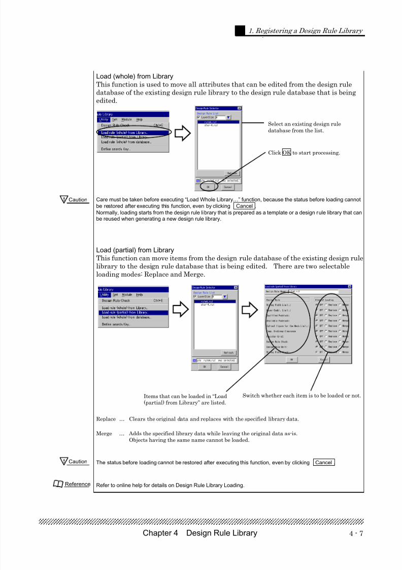
Load (whole) from Library
This function is used to move all attributes that can be edited from the design ruledatabase of the existing design rule library to the design rule database that is being
edited.
Select an existing design ruledatabase from the list.
Click OK to start processing.
Care must be taken before executing “Load Whole Library…” function, because the status before loading cannotbe restored after executing this function, even by clicking Cancel .
Normally, loading starts from the design rule library that is prepared as a template or a design rule library that canbe reused when generating a new design rule library.
Load (partial) from Library
This function can move items from the design rule database of the existing design rulelibrary to the design rule database that is being edited. There are two selectableloading modes: Replace and Merge.
Replace … Clears the original data and replaces with the specified library data.
Merge … Adds the specified library data while leaving the original data as-is.Objects having the same name cannot be loaded.
The status before loading cannot be restored after executing this function, even by clicking Cancel .
Refer to online help for details on Design Rule Library Loading.
Caution
Caution
Reference
Items that can be loaded in “Load(partial) from Library” are listed.
Switch whether each item is to be loaded or not.
7/27/2019 Design Library Master Training_cr
http://slidepdf.com/reader/full/design-library-master-trainingcr 54/89
Chapter 4 Design Rule Library4 - 8
1. Registering a Design Rule Library
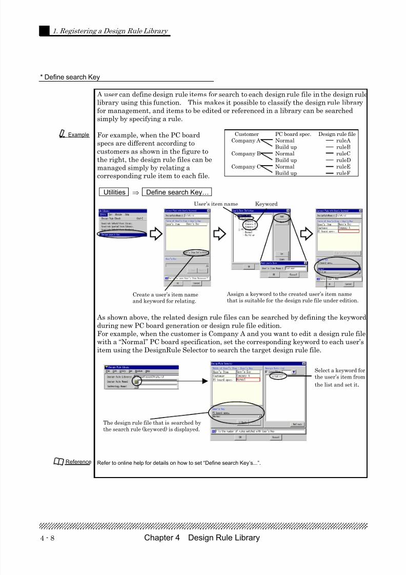
* Define search Key
A user can define design rule items for search to each design rule file in the design rule
library using this function. This makes it possible to classify the design rule libraryfor management, and items to be edited or referenced in a library can be searchedsimply by specifying a rule.
For example, when the PC boardspecs are different according tocustomers as shown in the figure tothe right, the design rule files can bemanaged simply by relating acorresponding rule item to each file.
Utilities ⇒ Define search Key…
User’s item name Keyword
As shown above, the related design rule files can be searched by defining the keywordduring new PC board generation or design rule file edition.For example, when the customer is Company A and you want to edit a design rule filewith a “Normal” PC board specification, set the corresponding keyword to each user’sitem using the DesignRule Selector to search the target design rule file.
Refer to online help for details on how to set “Define search Key’s...”.
Customer PC board spec. Design rule fileCompany A Normal ruleA
Build up ruleBCompany B Normal ruleC
Build up ruleDCompany C Normal ruleE
Build up ruleF
Example
Reference
Create a user’s item name
and keyword for relating.
Assign a keyword to the created user’s item name
that is suitable for the design rule file under edition.
Select a keyword forthe user’s item from
the list and set it.
The design rule file that is searched bythe search rule (keyword) is displayed.
7/27/2019 Design Library Master Training_cr
http://slidepdf.com/reader/full/design-library-master-trainingcr 55/89
4 - 9Chapter 4 Design Rule Library
1. Registering a Design Rule Library
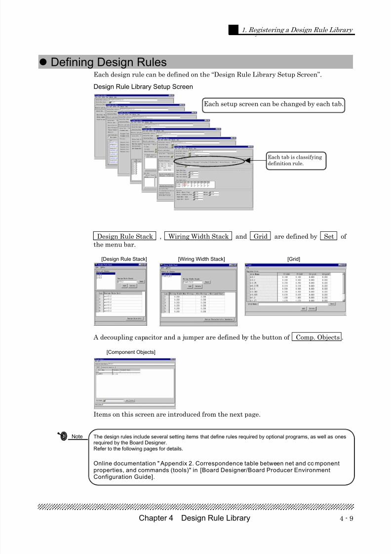
Each design rule can be defined on the “Design Rule Library Setup Screen”.
Design Rule Library Setup Screen
Design Rule Stack , Wiring Width Stack and Grid are defined by Set ofthe menu bar.
[Design Rule Stack] [Wiring Width Stack] [Grid]
A decoupling capacitor and a jumper are defined by the button of Comp. Objects .
[Component Objects]
Items on this screen are introduced from the next page.
The design rules include several setting items that define rules required by optional programs, as well as onesrequired by the Board Designer.Refer to the following pages for details.
Online documentation " Appendix 2. Correspondence table between net and componentproperties, and commands (tools)" in [Board Designer/Board Producer EnvironmentConfiguration Guide].
Defining Design Rules
Note
Each setup screen can be changed by each tab.
Each tab is classifyingdefinition rule.
7/27/2019 Design Library Master Training_cr
http://slidepdf.com/reader/full/design-library-master-trainingcr 56/89
Chapter 4 Design Rule Library4 - 10
1. Registering a Design Rule Library
Enter a name thatrepresents the PC board
material. (Can be omitted)
Specify the PC board thickness.Specify the thermal conductivitytransmitted in the PC board.
Size of square including thePC board.This setting is referenced toestimate and determine thescreen display area in thebeginning of the layout design.Be sure to enter this setting,even a rough value is allowed.This value is also referencedby the auto router.
Specify whether thereis a core layer.
Define the attribute for eachconductive/insulate layer.
Layer thickness/Material/Dielectric constant
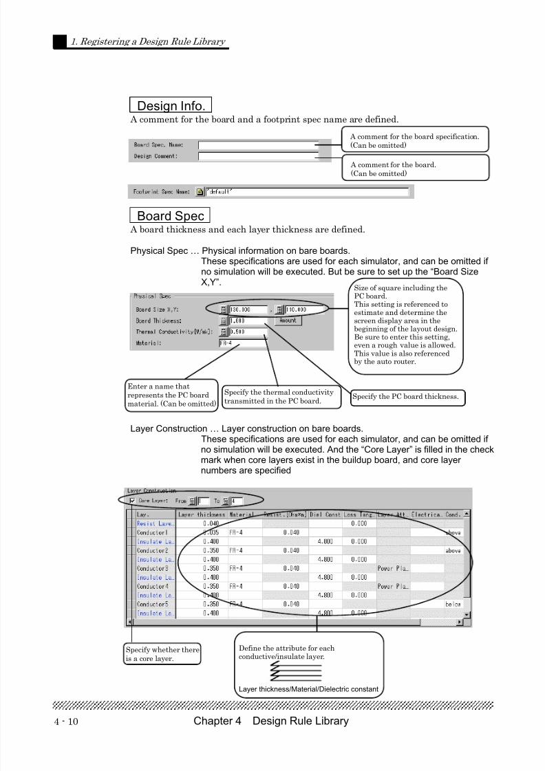
Design Info. A comment for the board and a footprint spec name are defined.
Board Spec A board thickness and each layer thickness are defined.
Physical Spec … Physical information on bare boards.These specifications are used for each simulator, and can be omitted if
no simulation will be executed. But be sure to set up the “Board SizeX,Y”.
Layer Construction … Layer construction on bare boards.These specifications are used for each simulator, and can be omitted ifno simulation will be executed. And the “Core Layer” is filled in the checkmark when core layers exist in the buildup board, and core layernumbers are specified
A comment for the board specification.(Can be omitted)
A comment for the board.(Can be omitted)
7/27/2019 Design Library Master Training_cr
http://slidepdf.com/reader/full/design-library-master-trainingcr 57/89
4 - 11Chapter 4 Design Rule Library
1. Registering a Design Rule Library
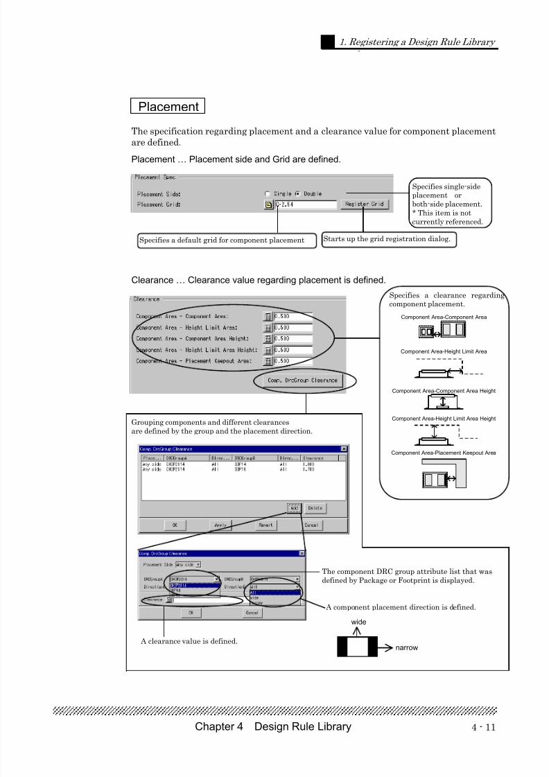
Placement
The specification regarding placement and a clearance value for component placementare defined.
Placement … Placement side and Grid are defined.
Clearance … Clearance value regarding placement is defined.
Grouping components and different clearancesare defined by the group and the placement direction.
Specifies a default grid for component placement
Specifies single-sideplacement orboth-side placement.* This item is notcurrently referenced.
Starts up the grid registration dialog.
Component Area-Component Area
Component Area-Component Area Height
Component Area-Height Limit Area Height
Component Area-Placement Keepout Area
Component Area-Height Limit Area
Specifies a clearance regardingcomponent placement.
A clearance value is defined.
The component DRC group attribute list that wasdefined by Package or Footprint is displayed.
A component placement direction is defined.
wide
narrow
7/27/2019 Design Library Master Training_cr
http://slidepdf.com/reader/full/design-library-master-trainingcr 58/89
Chapter 4 Design Rule Library4 - 12
1. Registering a Design Rule Library
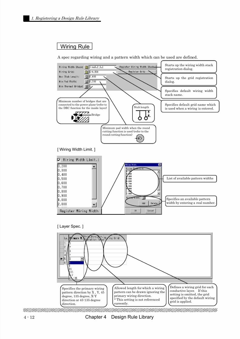
Wiring Rule
A spec regarding wiring and a pattern width which can be used are defined.
[ Wiring Width Limit. ]
[ Layer Spec. ]
Minimum number of bridges that areconnected to the power plane (refer tothe DRC function for the inside layer)
Bridge
Minimum pad width when the roundcutting function is used (refer to theround cutting function)
Stub length
Starts up the wiring width stackregistration dialog.
Starts up the grid registrationdialog.
Specifies default wiring widthstack name.
Specifies default grid name whichis used when a wiring is entered.
List of available pattern widths
Specifies an available patternwidth by entering a real number.
Defines a wiring grid for eachconductive layer. If thissetting is omitted, the grid
specified by the default wiringgrid is applied.
Specifies the primary wiringpattern direction by X , Y, 45
degree, 135 degree, X-Ydirection or 45-135 degreedirection.
Allowed length for which a wiringpattern can be drawn ignoring the
primary wiring direction.* This setting is not referencedcurrently.
7/27/2019 Design Library Master Training_cr
http://slidepdf.com/reader/full/design-library-master-trainingcr 59/89
4 - 13Chapter 4 Design Rule Library
1. Registering a Design Rule Library
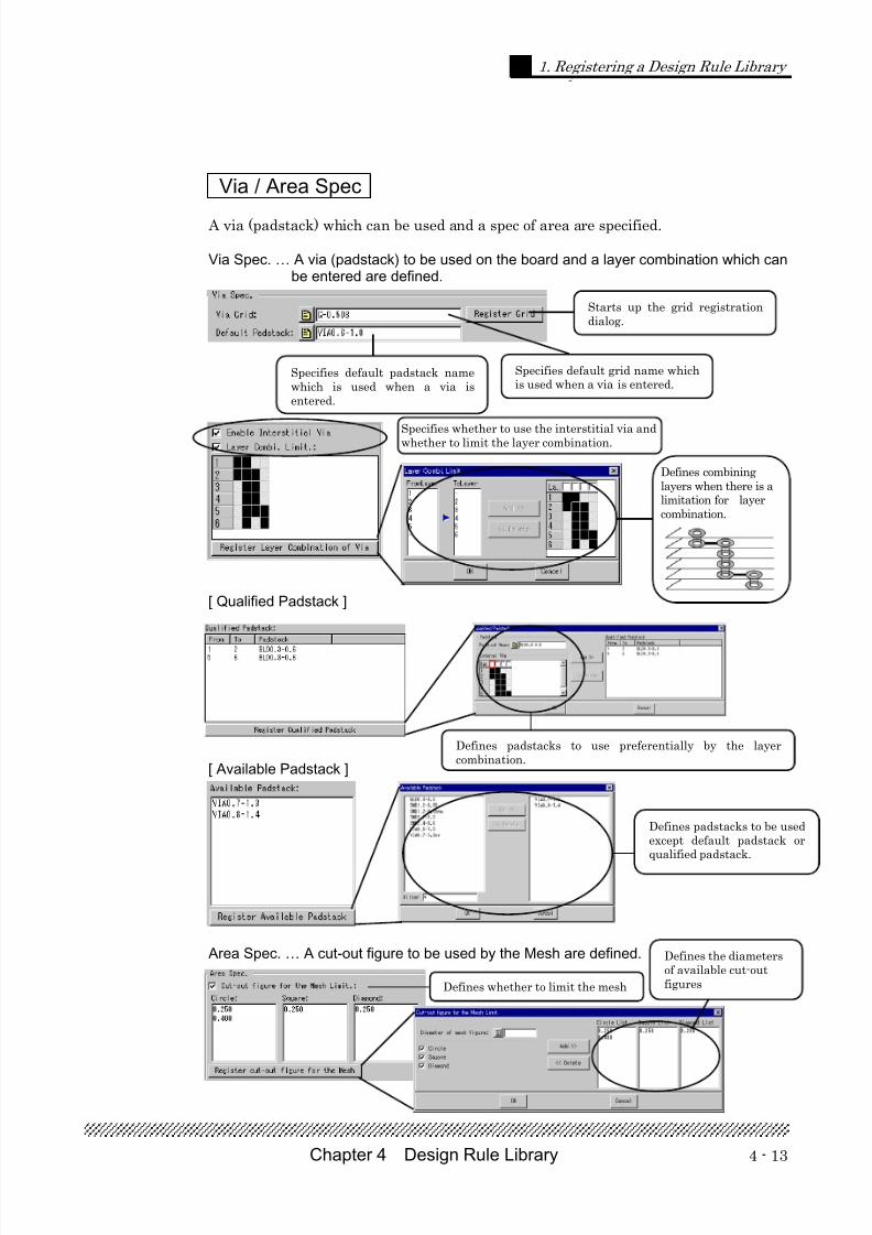
Via / Area Spec
A via (padstack) which can be used and a spec of area are specified.
Via Spec. … A via (padstack) to be used on the board and a layer combination which canbe entered are defined.
[ Qualified Padstack ]
[ Available Padstack ]
Area Spec. … A cut-out figure to be used by the Mesh are defined.
Starts up the grid registrationdialog.
Specifies default grid name whichis used when a via is entered.
Specifies default padstack namewhich is used when a via isentered.
Defines combininglayers when there is alimitation for layercombination.
Specifies whether to use the interstitial via andwhether to limit the layer combination.
Defines padstacks to use preferentially by the layercombination.
Defines padstacks to be usedexcept default padstack orqualified padstack.
Defines whether to limit the mesh
Defines the diametersof available cut-outfigures
7/27/2019 Design Library Master Training_cr
http://slidepdf.com/reader/full/design-library-master-trainingcr 60/89
Chapter 4 Design Rule Library4 - 14
1. Registering a Design Rule Library
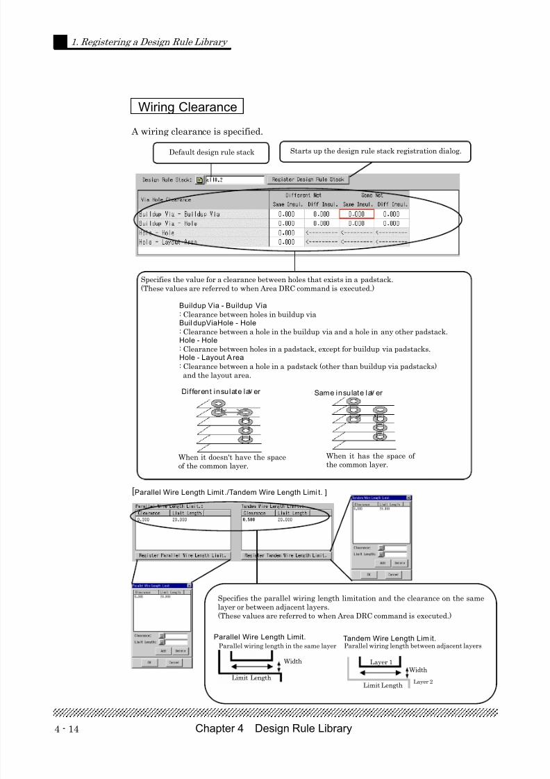
Wiring Clearance
A wiring clearance is specified.
[Parallel Wire Length Limit ./Tandem Wire Length Limi t. ]
Parallel wiring length in the same layer
Width
Limit Length
Parallel wiring length between adjacent layers
Layer 1Width
Limit Length Layer 2
Parallel Wire Length Limit. Tandem Wire Length Lim it.
Specifies the parallel wiring length limitation and the clearance on the samelayer or between adjacent layers.(These values are referred to when Area DRC command is executed.)
Default design rule stack Starts up the design rule stack registration dialog.
Specifies the value for a clearance between holes that exists in a padstack.(These values are referred to when Area DRC command is executed.)
Buildup Via - Buildup Via
: Clearance between holes in buildup viaBuildupViaHole - Hole
: Clearance between a hole in the buildup via and a hole in any other padstack.Hole - Hole
: Clearance between holes in a padstack, except for buildup via padstacks.Hole - Layout Area
: Clearance between a hole in a padstack (other than buildup via padstacks)and the layout area.
Dif ferent insulate la er Same insulate la er
When it doesn't have the spaceof the common layer.
When it has the space ofthe common layer.
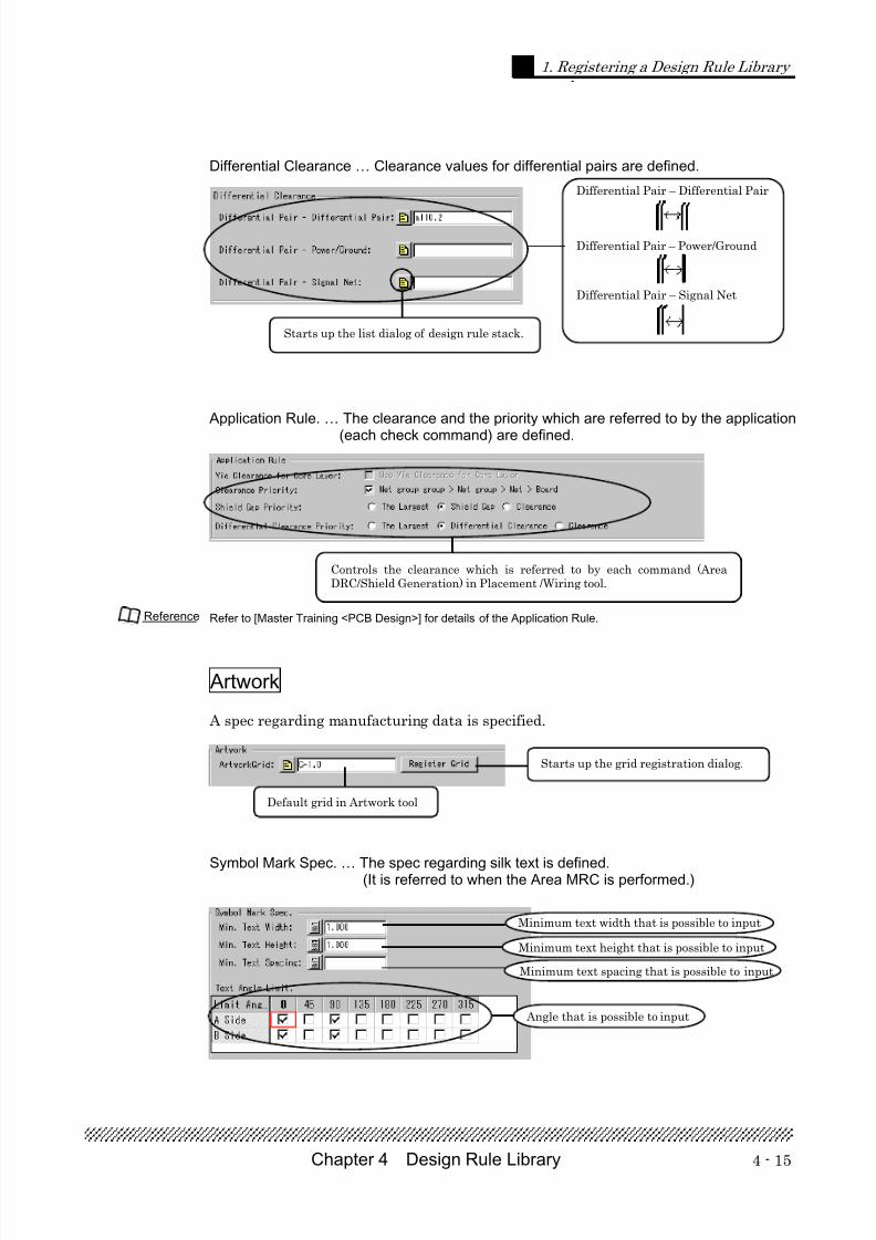
7/27/2019 Design Library Master Training_cr
http://slidepdf.com/reader/full/design-library-master-trainingcr 61/89
4 - 15Chapter 4 Design Rule Library
1. Registering a Design Rule Library
Starts up the list dialog of design rule stack.
Differential Clearance … Clearance values for differential pairs are defined.
Application Rule. … The clearance and the priority which are referred to by the application
(each check command) are defined.
Refer to [Master Training <PCB Design>] for details of the Application Rule.
Artwork
A spec regarding manufacturing data is specified.
Symbol Mark Spec. … The spec regarding silk text is defined.(It is referred to when the Area MRC is performed.)
Reference
Starts up the grid registration dialog.
Default grid in Artwork tool
Minimum text width that is possible to input
Minimum text height that is possible to input
Minimum text spacing that is possible to input
Angle that is possible to input
Controls the clearance which is referred to by each command (AreaDRC/Shield Generation) in Placement /Wiring tool.
Differential Pair – Differential Pair
Differential Pair – Power/Ground
Differential Pair – Signal Net
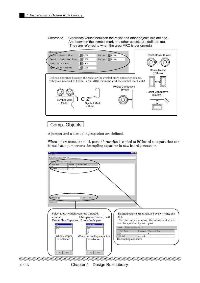
7/27/2019 Design Library Master Training_cr
http://slidepdf.com/reader/full/design-library-master-trainingcr 62/89
Chapter 4 Design Rule Library4 - 16
1. Registering a Design Rule Library
Clearance … Clearance values between the resist and other objects are defined. And between the symbol mark and other objects are defined, too.(They are referred to when the area MRC is performed.)
Comp. Objects
A jumper and a decoupling capacitor are defined.
When a part name is added, part information is copied to PC board as a part that canbe used as a jumper or a decoupling capacitor in new board generation.
Resist-Conductive(Reflow)
Defines clearance between the resist or the symbol mark and other objects.(They are referred to by the area MRC command and the symbol mark cut.)
Symbol Mark- Resist Symbol Mark
- Hole
Resist-Conductive (Flow)
Resist-Resist (Flow)
Resist-Resist(Reflow)
Select a part which registers and add. Defined objects are displayed by switching thetab.The placement side and the placement anglecan be specified by each part.
Jumper : Jumper attribute (Part)Decoupling Capacitor : 2-terminals part
Decoupling capacitorWhen Jumper
is selected When decoupling capacitor
is selected
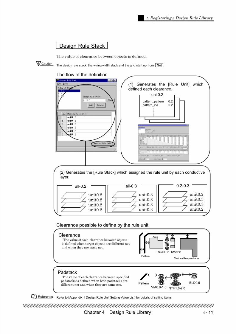
7/27/2019 Design Library Master Training_cr
http://slidepdf.com/reader/full/design-library-master-trainingcr 63/89
4 - 17Chapter 4 Design Rule Library
1. Registering a Design Rule Library
Design Rule Stack
The value of clearance between objects is defined.
The design rule stack, the wiring width stack and the grid start up from Set .
The flow of the definition
Clearance possible to define by the rule unit
Refer to [Appendix 1 Design Rule Unit Setting Value List] for details of setting items.
Caution
(1) Generates the [Rule Unit] whichdefined each clearance.
unit0.2
pattern_pattern 0.2pattern_via 0.2
(2) Generates the [Rule Stack] which assigned the rule unit by each conductive
layer.
unit0.2unit0.2unit0.2unit0.2
all-0.2
unit0.3unit0.3unit0.3unit0.3
all-0.3
unit0.2unit0.3unit0.3unit0.2
0.2-0.3
ClearanceThe value of each clearance between objects
is defined when target objects are different netand when they are same net.
Pattern
Though Pin SMD Pin
Various Keep-out area
Area
PadstackThe value of each clearance between specified
padstacks is defined when both padstacks aredifferent net and when they are same net.
VIA0.8-1.5 NTH1.0-2.0
BLD0.5Pattern
Reference
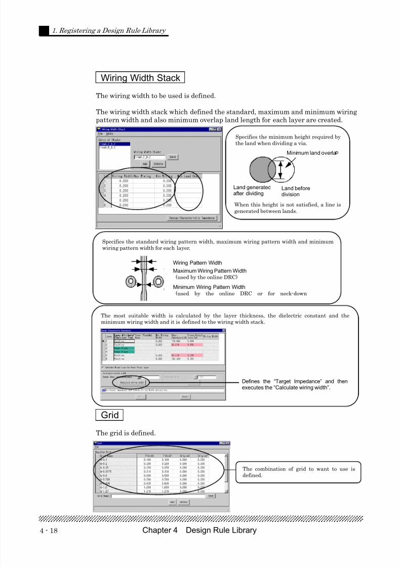
7/27/2019 Design Library Master Training_cr
http://slidepdf.com/reader/full/design-library-master-trainingcr 64/89
Chapter 4 Design Rule Library4 - 18
1. Registering a Design Rule Library
Wiring Width Stack
The wiring width to be used is defined.
The wiring width stack which defined the standard, maximum and minimum wiringpattern width and also minimum overlap land length for each layer are created.
Grid
The grid is defined.
The most suitable width is calculated by the layer thickness, the dielectric constant and theminimum wiring width and it is defined to the wiring width stack.
Specifies the minimum height required bythe land when dividing a via.
Minimum land overla
Land generatedafter dividing
Land beforedivision
When this height is not satisfied, a line isgenerated between lands.
Specifies the standard wiring pattern width, maximum wiring pattern width and minimumwiring pattern width for each layer.
Wiring Pattern Width
Maximum Wiring Pattern Width(used by the online DRC)
Minimum Wiring Pattern Width
(used by the online DRC or for neck-down
Defines the “Target Impedance” and thenexecutes the “Calculate wiring width”.
The combination of grid to want to use isdefined.
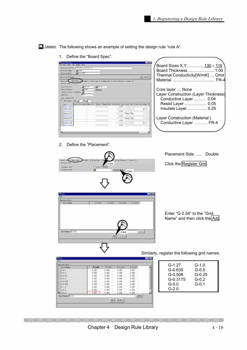
7/27/2019 Design Library Master Training_cr
http://slidepdf.com/reader/full/design-library-master-trainingcr 65/89
4 - 19Chapter 4 Design Rule Library
1. Registering a Design Rule Library
The following shows an example of setting the design rule “rule A”.
1. Define the “Board Spec”.
2. Define the “Placement”.
Placement Side ….. Double
Click the Register Grid.
Enter “G-2.54” to the “Grid
Name” and then click the Add.
Similarly, register the following grid names.
Lesson
Board Sizes X,Y………… 130 × 110Board Thickness …………….... 1.00Thermal Conductivity[W/mK] … OmitMaterial ……………………….… FR-4 Core layer … NoneLayer Construction (Layer Thickness) Conductive Layer ……… 0.04
Resist Layer ……………. 0.05Insulate Layer ………….. 0.25
Layer Construction (Material )
Conductive Layer ………. FR-4
G-1.27 G-1.0G-0.635 G-0.5G-0.508 G-0.25G-0.3175 G-0.2G-5.0 G-0.1G-2.0
Click
Click
Click
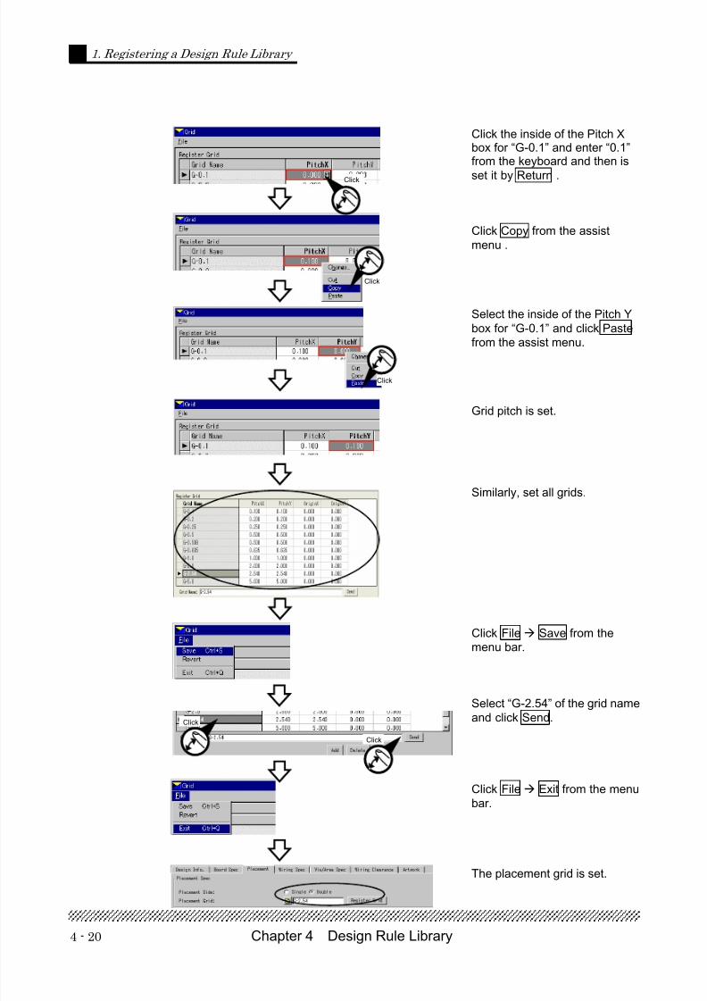
7/27/2019 Design Library Master Training_cr
http://slidepdf.com/reader/full/design-library-master-trainingcr 66/89
Chapter 4 Design Rule Library4 - 20
1. Registering a Design Rule Library
Click the inside of the Pitch Xbox for “G-0.1” and enter “0.1”from the keyboard and then is
set it by Return .
Click Copy from the assist
menu .
Select the inside of the Pitch Y
box for “G-0.1” and click Paste
from the assist menu.
Grid pitch is set.
Similarly, set all grids.
Click File Save from the
menu bar.
Select “G-2.54” of the grid nameand click Send.
Click File Exit from the menu
bar.
The placement grid is set.
Click
Click
Click
Click
Click
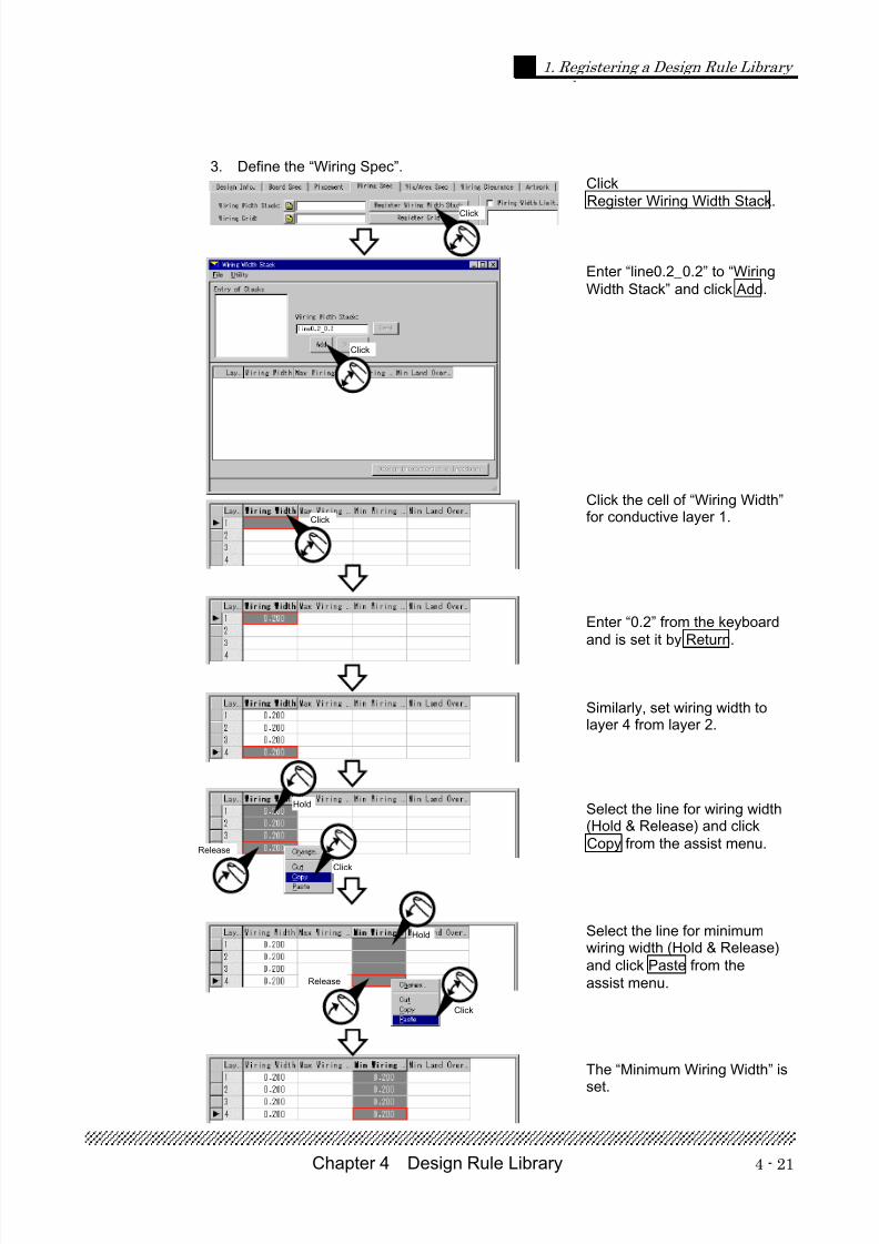
7/27/2019 Design Library Master Training_cr
http://slidepdf.com/reader/full/design-library-master-trainingcr 67/89
4 - 21Chapter 4 Design Rule Library
1. Registering a Design Rule Library
3. Define the “Wiring Spec”.Click
Register Wiring Width Stack.
Enter “line0.2_0.2” to “Wiring
Width Stack” and click Add.
Click the cell of “Wiring Width”for conductive layer 1.
Enter “0.2” from the keyboard
and is set it by Return.
Similarly, set wiring width tolayer 4 from layer 2.
Select the line for wiring width(Hold & Release) and click
Copy from the assist menu.
Select the line for minimumwiring width (Hold & Release)
and click Paste from the
assist menu.
The “Minimum Wiring Width” is
set.
Click
Click
Click
Release
Click
Release
Hold
Hold
Click
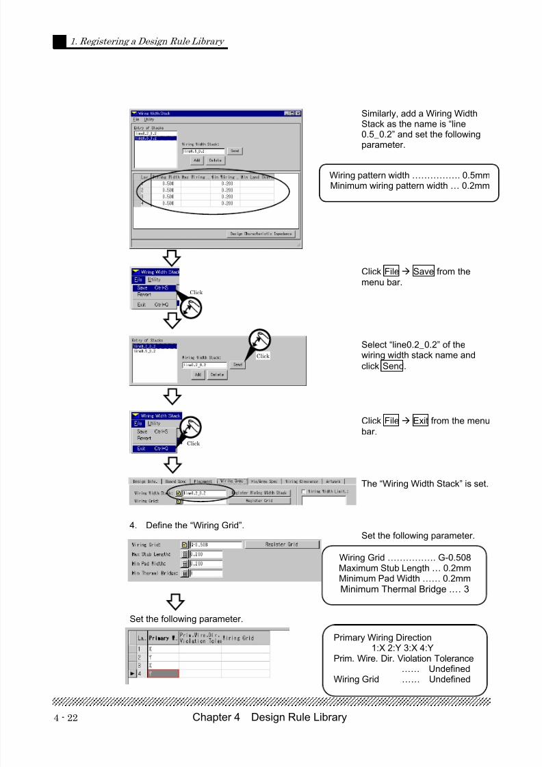
7/27/2019 Design Library Master Training_cr
http://slidepdf.com/reader/full/design-library-master-trainingcr 68/89
Chapter 4 Design Rule Library4 - 22
1. Registering a Design Rule Library
Similarly, add a Wiring WidthStack as the name is “line
0.5_0.2” and set the followingparameter.
Click File Save from themenu bar.
Select “line0.2_0.2” of thewiring width stack name and
click Send.
Click File Exit from the menu
bar.
The “Wiring Width Stack” is set.
4. Define the “Wiring Grid”.
Set the following parameter.
Set the following parameter.
Wiring pattern width ……………. 0.5mmMinimum wiring pattern width … 0.2mm
Wiring Grid ……………. G-0.508Maximum Stub Length … 0.2mmMinimum Pad Width …… 0.2mm
Minimum Thermal Bridge .… 3
Primary Wiring Direction1:X 2:Y 3:X 4:Y
Prim. Wire. Dir. Violation Tolerance
…… UndefinedWiring Grid …… Undefined
Click
Click
Click
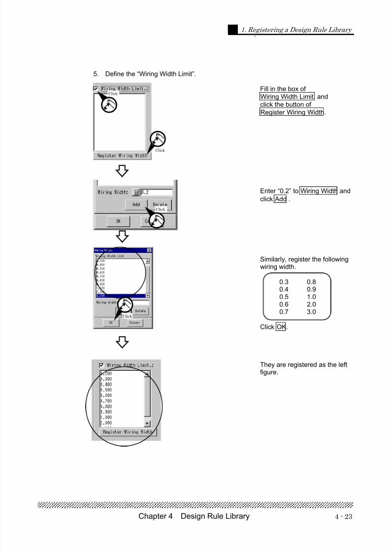
7/27/2019 Design Library Master Training_cr
http://slidepdf.com/reader/full/design-library-master-trainingcr 69/89
4 - 23Chapter 4 Design Rule Library
1. Registering a Design Rule Library
5. Define the “Wiring Width Limit”.
Fill in the box of
Wiring Width Limit. andclick the button of
Register Wiring Width.
Enter “0.2” to Wiring Width andclick Add .
Similarly, register the followingwiring width.
Click OK.
They are registered as the leftfigure.
0.3 0.8
0.4 0.90.5 1.00.6 2.00.7 3.0
Click
Click
Click
Click
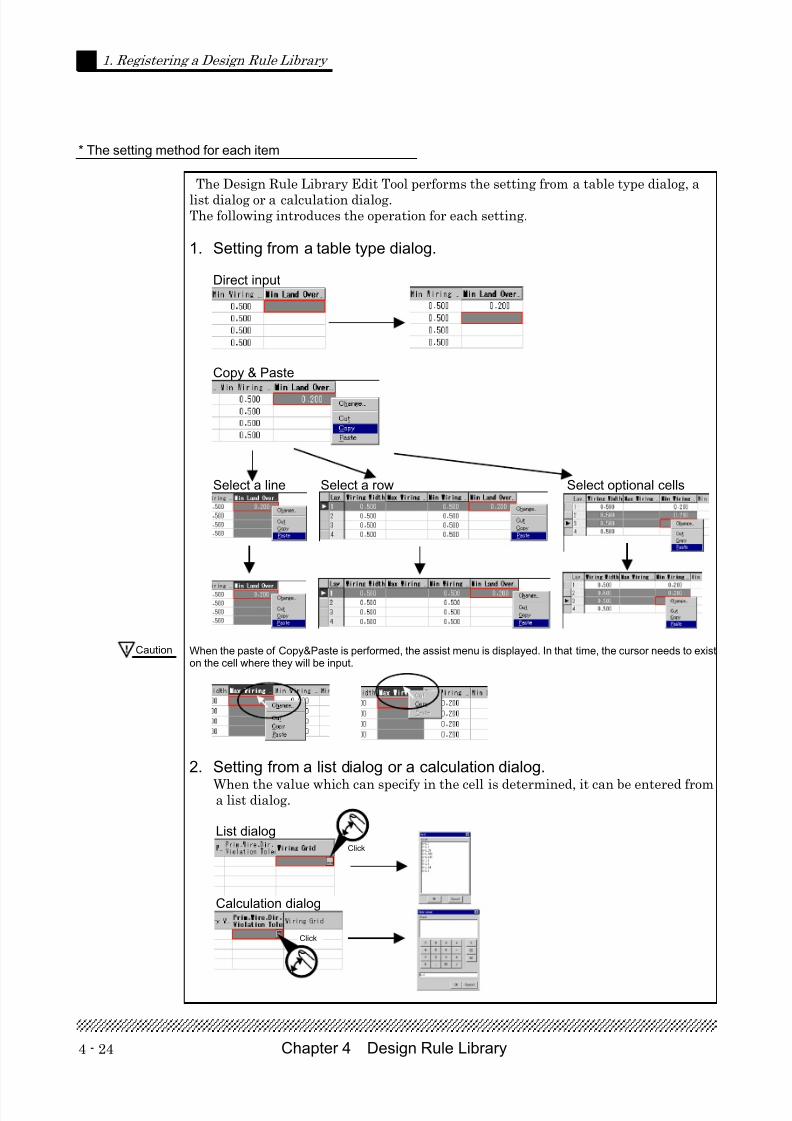
7/27/2019 Design Library Master Training_cr
http://slidepdf.com/reader/full/design-library-master-trainingcr 70/89
Chapter 4 Design Rule Library4 - 24
1. Registering a Design Rule Library
* The setting method for each item
The Design Rule Library Edit Tool performs the setting from a table type dialog, a
list dialog or a calculation dialog.The following introduces the operation for each setting.
1. Setting from a table type dialog.
Direct input
Copy & Paste
Select a line Select a row Select optional cells
When the paste of Copy&Paste is performed, the assist menu is displayed. In that time, the cursor needs to existon the cell where they will be input.
2. Setting from a list dialog or a calculation dialog.
When the value which can specify in the cell is determined, it can be entered froma list dialog.
List dialog
Calculation dialog
Caution
Click
Click
7/27/2019 Design Library Master Training_cr
http://slidepdf.com/reader/full/design-library-master-trainingcr 71/89
4 - 25Chapter 4 Design Rule Library
1. Registering a Design Rule Library
6. Define the “Via/Area Spec”.Click the list icon for via grid.
Select “G-0.508” from the list
and click OK .
Click the list icon for defaultpadstack.
Select “V0.6-1.0” from the list
and click OK.
The via spec. is set as the leftfigure.
7. Define the “Available Padstack”.Click
Register Available Padstack.
Select “VIA0.7-1.3" and
“VIA0.8-1.4” pressing Ctrl key,
and click Add.
Ctrl key, and click Add .
Click
Click
Click
Click
Click
Click
Click
Click
Click

7/27/2019 Design Library Master Training_cr
http://slidepdf.com/reader/full/design-library-master-trainingcr 72/89
Chapter 4 Design Rule Library4 - 26
1. Registering a Design Rule Library
Click OK.
The available padstack is set asthe left figure.
Other Via/Area spec. isundefined.
8. Define the “Wiring Clearance”.Click
Register Design Rule Stack.
Click Design Rule Unit from
the started up dialog.
Enter “unit0.2” to “design Rule
Stack” and click Add.
Click
Click
Click
Click
7/27/2019 Design Library Master Training_cr
http://slidepdf.com/reader/full/design-library-master-trainingcr 73/89
4 - 27Chapter 4 Design Rule Library
1. Registering a Design Rule Library
Click Utilities
Fill all clearance… from the
menu bar.
Enter “0.2” and click OK.
"0.2" is set as the left figure toall the cells.
Refer to [*The setting method for each item] on page 4-24, for other input method.
The clearance for Padstack isundefined.
Similarly, add a rule unit as thename is “unit0.3” and set thefollowing clearance.
Click
Reference
Clearance … 0.3mm for allPadstack …. Undefined
Click
7/27/2019 Design Library Master Training_cr
http://slidepdf.com/reader/full/design-library-master-trainingcr 74/89
Chapter 4 Design Rule Library4 - 28
1. Registering a Design Rule Library
Click File Exit from the menu
bar.
Click Yes from the confirmation
dialog.
Register a Design Rule Unit and register a design rule stack.Enter “all-0.2” to the “Design
Rule Stack” and click Add.
Select the cell of “Design RuleUnit” for conductive layer1 andclick the action button.
Select “unit0.2” and click OK.
Click
Click
Click
Click
Click
Click
7/27/2019 Design Library Master Training_cr
http://slidepdf.com/reader/full/design-library-master-trainingcr 75/89
4 - 29Chapter 4 Design Rule Library
1. Registering a Design Rule Library
Select the cell of the “DesignRule Unit” for layer 1 and click
Copy from the assist menu.
Select the line of the “DesignRule Unit” (Hold & Release) and
click Paste.
It is set as the left figure.
Similarly, add a design rulestack as the name is “all-0.3”and set the following parameter.
Click
Hold
Release
Click
Design Rule Unit … “unit0.3” for all
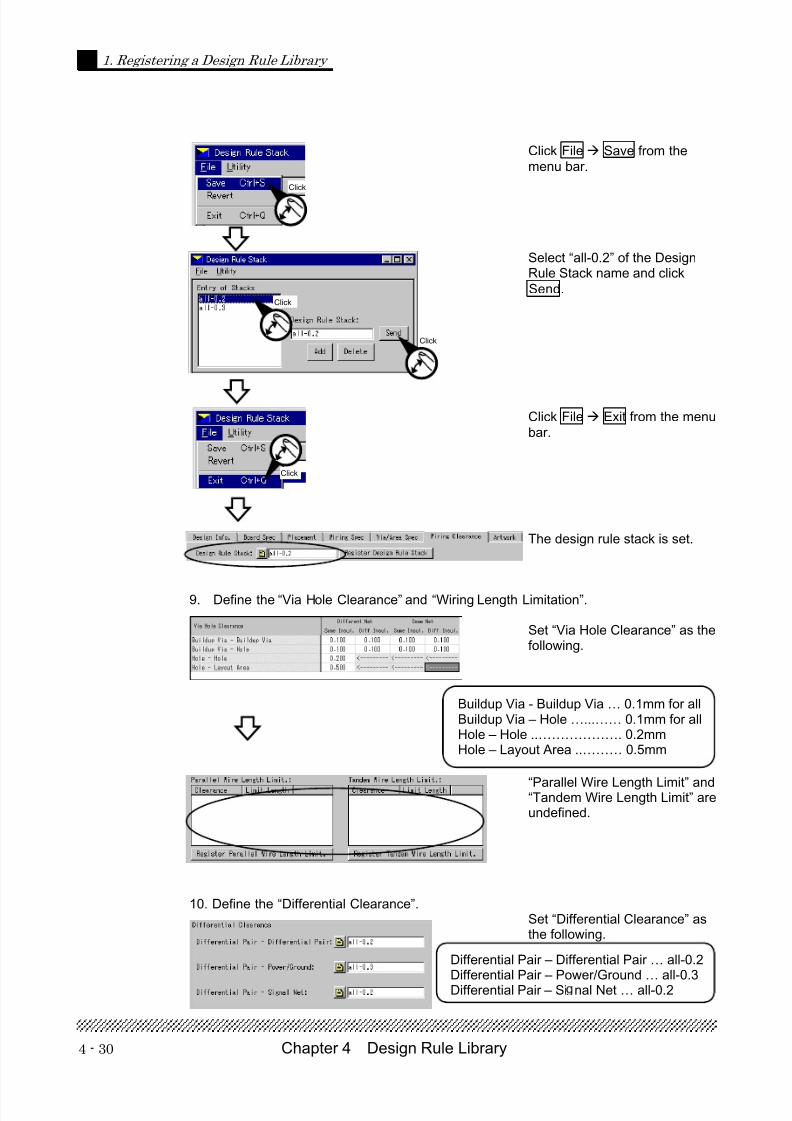
7/27/2019 Design Library Master Training_cr
http://slidepdf.com/reader/full/design-library-master-trainingcr 76/89
Chapter 4 Design Rule Library4 - 30
1. Registering a Design Rule Library
Click File Save from the
menu bar.
Select “all-0.2” of the DesignRule Stack name and click
Send.
Click File Exit from the menu
bar.
The design rule stack is set.
9. Define the “Via Hole Clearance” and “Wiring Length Limitation”.
Set “Via Hole Clearance” as thefollowing.
“Parallel Wire Length Limit” and“Tandem Wire Length Limit” areundefined.
10. Define the “Differential Clearance”.Set “Differential Clearance” asthe following.
Buildup Via - Buildup Via … 0.1mm for allBuildup Via – Hole …...…… 0.1mm for allHole – Hole ..………………. 0.2mmHole – Layout Area ..……… 0.5mm
Click
Click
Click
Click
Differential Pair – Differential Pair … all-0.2Differential Pair – Power/Ground … all-0.3Differential Pair – Si nal Net … all-0.2
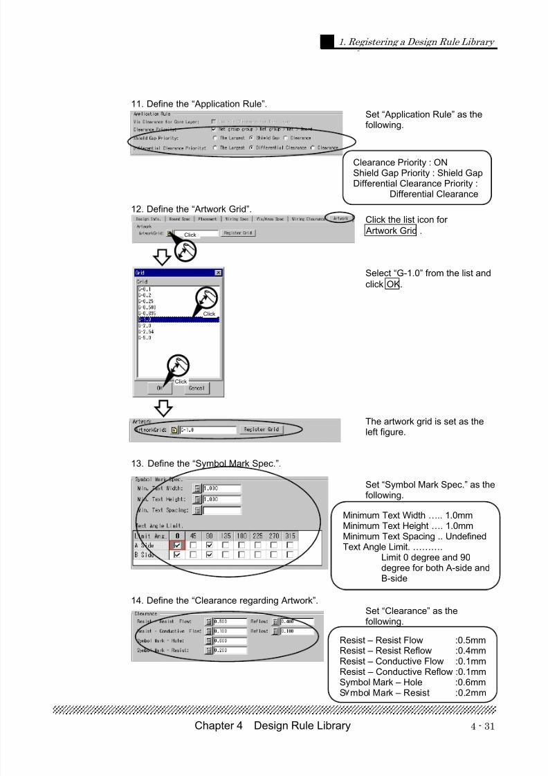
7/27/2019 Design Library Master Training_cr
http://slidepdf.com/reader/full/design-library-master-trainingcr 77/89
4 - 31Chapter 4 Design Rule Library
1. Registering a Design Rule Library
11. Define the “Application Rule”.Set “Application Rule” as thefollowing.
12. Define the “Artwork Grid”.Click the list icon for
Artwork Grid .
Select “G-1.0” from the list andclick OK.
The artwork grid is set as theleft figure.
13. Define the “Symbol Mark Spec.”.
Set “Symbol Mark Spec.” as thefollowing.
14. Define the “Clearance regarding Artwork”.Set “Clearance” as thefollowing.
Clearance Priority : ONShield Gap Priority : Shield GapDifferential Clearance Priority : Differential Clearance
Click
Click
Click
Minimum Text Width ….. 1.0mmMinimum Text Height …. 1.0mmMinimum Text Spacing .. Undefined
Text Angle Limit. ……….Limit 0 degree and 90degree for both A-side andB-side
Resist – Resist Flow :0.5mmResist – Resist Reflow :0.4mmResist – Conductive Flow :0.1mmResist – Conductive Reflow :0.1mm
Symbol Mark – Hole :0.6mmS mbol Mark – Resist :0.2mm
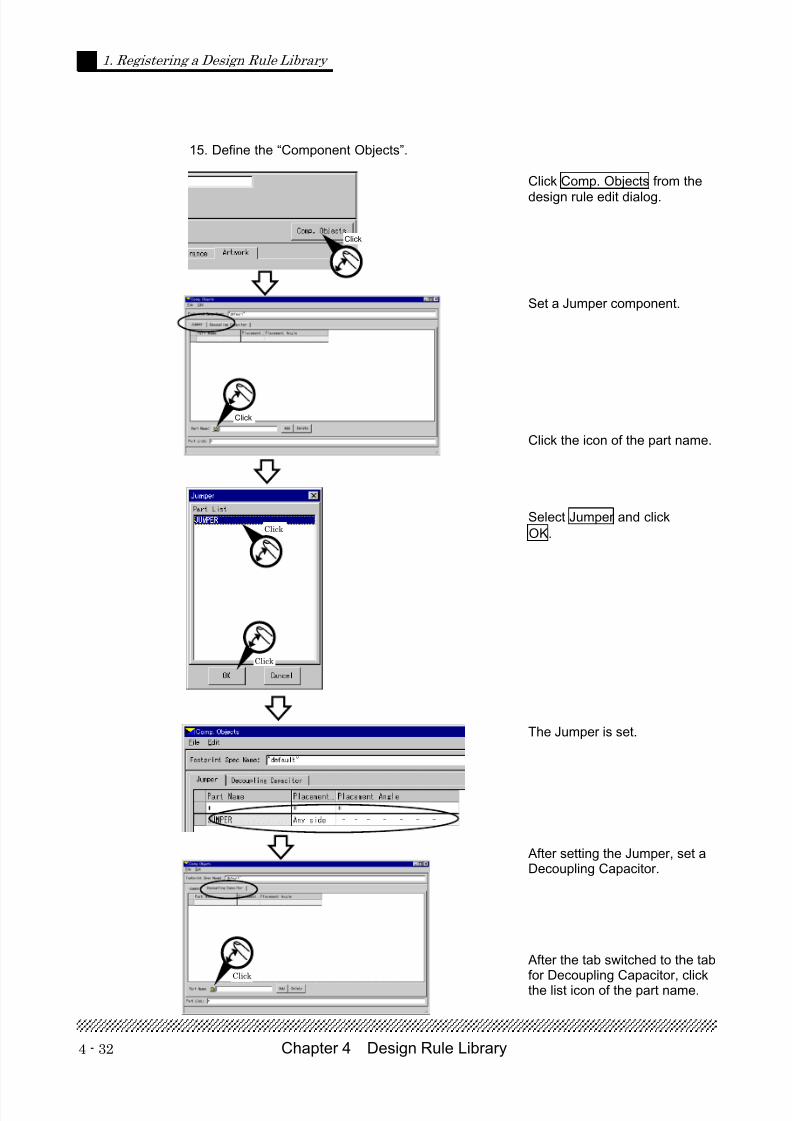
7/27/2019 Design Library Master Training_cr
http://slidepdf.com/reader/full/design-library-master-trainingcr 78/89
Chapter 4 Design Rule Library4 - 32
1. Registering a Design Rule Library
15. Define the “Component Objects”.
Click Comp. Objects from the
design rule edit dialog.
Set a Jumper component.
Click the icon of the part name.
Select Jumper and click
OK.
The Jumper is set.
After setting the Jumper, set aDecoupling Capacitor.
After the tab switched to the tab
for Decoupling Capacitor, clickthe list icon of the part name.
Click
Click
Click
Click
Click
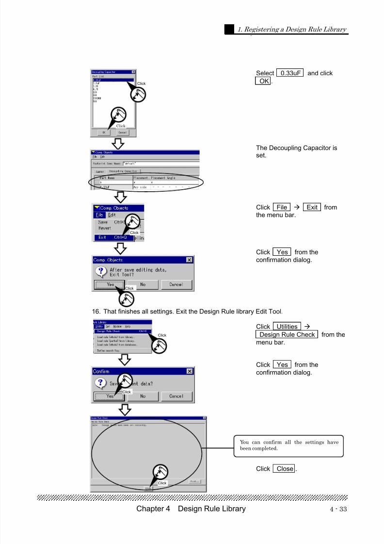
7/27/2019 Design Library Master Training_cr
http://slidepdf.com/reader/full/design-library-master-trainingcr 79/89
4 - 33Chapter 4 Design Rule Library
1. Registering a Design Rule Library
Select 0.33uF and click
OK .
The Decoupling Capacitor isset.
Click File Exit from
the menu bar.
Click Yes from the
confirmation dialog.
16. That finishes all settings. Exit the Design Rule library Edit Tool.
Click Utilities
Design Rule Check from the
menu bar.
Click Yes from the
confirmation dialog.
Click Close .
Click
Click
Click
Click
Click
You can confirm all the settings havebeen completed.
Click
Click
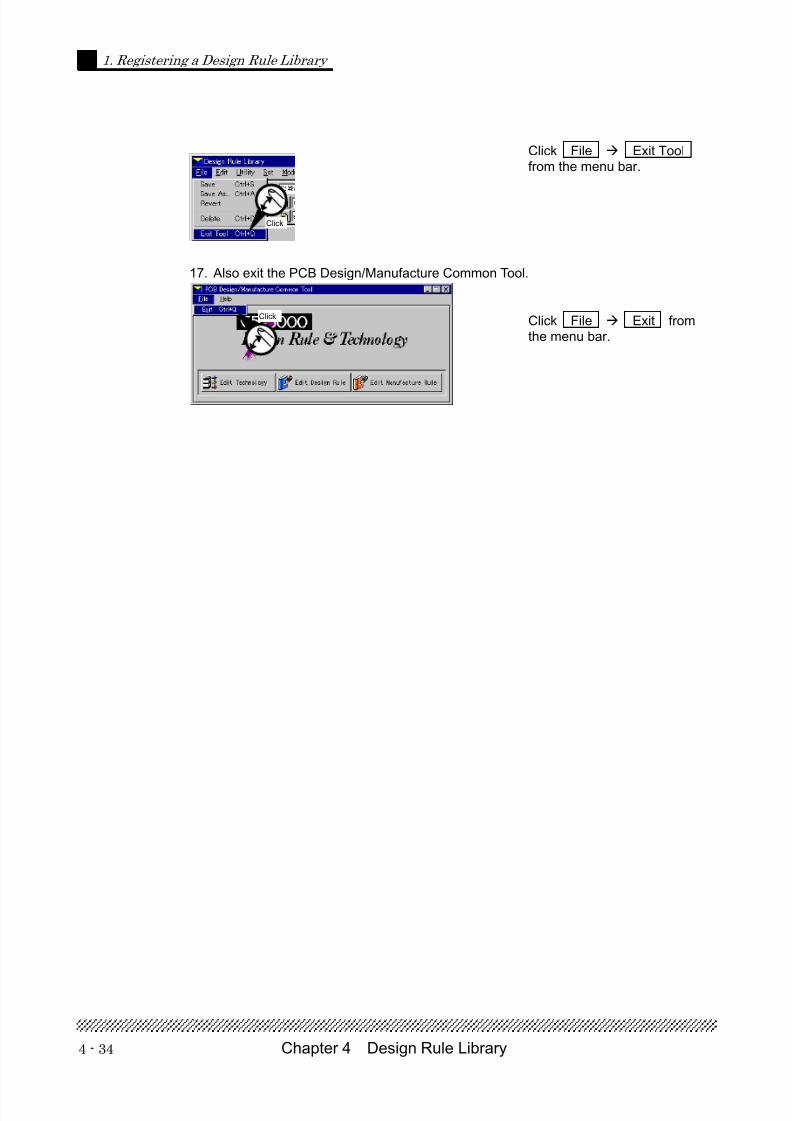
7/27/2019 Design Library Master Training_cr
http://slidepdf.com/reader/full/design-library-master-trainingcr 80/89
Chapter 4 Design Rule Library4 - 34
1. Registering a Design Rule Library
Click File Exit Tool
from the menu bar.
17. Also exit the PCB Design/Manufacture Common Tool.
Click File Exit from
the menu bar.
Click
Click
7/27/2019 Design Library Master Training_cr
http://slidepdf.com/reader/full/design-library-master-trainingcr 81/89
7/27/2019 Design Library Master Training_cr
http://slidepdf.com/reader/full/design-library-master-trainingcr 82/89
A - 1
1. Design Rule Unit Setting Value List
Appendix
Clearance value possible to set by the Design Rule UnitClearance value between the various objects are set by the Design Rule Unit.
Those details are introduced in the following.
ClearanceClearance value between the objects is defined at every combination of objects.(The following clearance value can be set by same net or different net.)
“ Clearance for Wiring (except Area)”Targert1 Target2
Wire (Except Area) A1
Area (Wire) A2
Through Pin A3
SMD Pin A4
Through Via A5
Internal Via A6
Landless Through Via A7
Landless Internal Via A8
Buildup Via A9
Skip/Stack A10
Landless Skip/Stack A11
Through Via in core layer A12
Internal Via in core layer A13
Landless Through Viain core layer
A14
Wire(Except Area)
Landless Internal Viain core layer
A15
Through Via in core layer/Internal Via in core layer/Landless Through Via in core layer/ Landless Internal Via in
core layer can be defined when Via Clearance for Core Layer in Wiring Clearance - Application Rule is
filled in.
“ Clearance for Area (Wiring)”Targert1 Target2
Area (Wire) B1
Through Pin B2
SMD Pin B3
Through Via B4
Internal Via B5
Landless Through ViaB6
Landless Internal Via B7
Buildup Via B8
Skip/Stack B9
Landless Skip/Stack B10
Through Via in core layer B11
Internal Via in core layer B12
Landless Through Viain core layer
B13
Area(Wire)
Landless Internal Viain core layer
B14
Note
B3
B1
B2
B5B4
Through Via Internal Via
B6 B7
Landless
Through ViaLandless
Internal Via
B8
Buildup Via Skip/Stack
B10
Landless
Skip/Stack
B13
B14
Landless
Internal Via
in core layer
Landless
Through Via
in core layer
Through Via
in core layer
Internal Via
in core layer
B11
B12
A1
A4
A2
A3
A8
Landless
Through ViaLandless
Internal Via
A7
A10
Skip/Stack
A9 A11
Landless
Skip/Stack
A12
Internal Via
in core layer
A13 A15
A14
Landless
Internal Via
in core layer
Landless
Through Via
in core layer
Buildup Via
Through Via
in core layer
A6 A5
Through Via Internal Via
7/27/2019 Design Library Master Training_cr
http://slidepdf.com/reader/full/design-library-master-trainingcr 83/89
Appendix A - 2
1.Design Rule Unit Setting Value List
“ Clearance for Through Pin” Targert1 Target2
Through Pin C1
SMD Pin C2
Through Via C3
Internal Via C4
Landless Through Via C5
Landless Internal Via C6
Buildup Via C7
Skip/Stack C8
Landless Skip/Stack C9
Through Via in core layer C10
Internal Via in core layer C11
Landless Through Viain core layer
C12
ThroughPin
Landless Internal Via
in core layer C13
“ Clearance for SMD Pin” Targert1 Target2
SMD Pin D1
Through Via D2
Internal Via D3
Landless Through Via D4
Landless Internal Via D5
Buildup Via D6
Skip/Stack D7
Landless Skip/Stack D8
Through Via in core layer D9
Internal Via in core layer D10
Landless Through Viain core layer
D11
SMD
Pin
Landless Internal Viain core layer
D12
“ Clearance for Through Via” Targert1 Target2
Through Via E1
Internal Via E2Landless Through Via E3
Landless Internal Via E4
Buildup Via E5
Skip/Stack E6
Landless Skip/Stack E7
Through Via in core layer E8
Internal Via in core layer E9
Landless Through Viain core layer
E10
ThroughVia
Landless Internal Viain core layer
E11
Through Viain core layer
C6
Landless
Through Via
Landless
Inaternal Via
C5C4C3
Through Via Internal Via
C8
Skip/Stack
C7
C10
Internal Viain core layer
C11 C13C12
Landless
Internal Via
in core layer
Landless
Through Via
in core layer
C1C2
C9
Landless
Skip/StackBuildup Via
D1
D
3D2
D6 D7 D8
D11
D12
D9
D10
D4 D5
Through Via Internal ViaLandless
Through Via
Landless
Inaternal Via
Skip/StackBuildup ViaLandless
Skip/Stack
Through Via
in core layer
Internal Via
in core layer
Landless
Internal Via
in core layer
Landless
Through Via
in core layer
C6C5C4C3
C10 C11 C13C12
C9C8C7
Through Via
in core layer
Internal Via
in core layer
Landless
Internal Via
in core layer
Landless
Through Via
in core layer
Skip/StackLandless
Skip/StackBuildup Via
LandlessThrough Via
LandlessInaternal Via
Through Via Internal Via
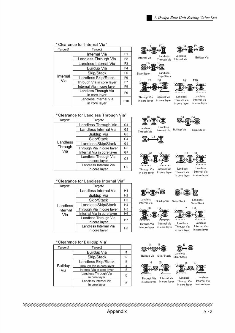
7/27/2019 Design Library Master Training_cr
http://slidepdf.com/reader/full/design-library-master-trainingcr 84/89
A - 3 Appendix
1. Design Rule Unit Setting Value List
“ Clearance for Internal Via”
“ Clearance for Landless Through Via”
“ Clearance for Landless Internal Via”
“ Clearance for Buildup Via”
Targert1 Target2
Internal Via F1
Landless Through Via F2
Landless Internal Via F3
Buildup Via F4
Skip/Stack F5
Landless Skip/Stack F6
Through Via in core layer F7
Internal Via in core layer F8
Landless Through Viain core layer
F9
InternalVia
Landless Internal Viain core layer
F10
Targert1 Target2
Landless Through Via G1
Landless Internal Via G2
Buildup Via G3
Skip/Stack G4
Landless Skip/Stack G5
Through Via in core layer G6
Internal Via in core layer G7
Landless Through Viain core layer
G8
LandlessThrough
Via
Landless Internal Viain core layer
G9
Targert1 Target2
Landless Internal Via H1
Buildup Via H2
Skip/Stack H3
Landless Skip/Stack H4
Through Via in core layer H5
Internal Via in core layer H6
Landless Through Viain core layer
H7
LandlessInternal
Via
Landless Internal Viain core layer
H8
Targert1 Target2
Buildup Via I1
Skip/Stack I2
Landless Skip/Stack I3
Through Via in core layer I4
Internal Via in core layer I5
Landless Through Viain core layer
I6
BuildupVia
Landless Internal Viain core layer
I7
F4F3F2F1
F7 F8 F10F9
F6F5
Landless
Through Via
Landless
Internal Via
Skip/Stack Landless
Skip/Stack
Internal Via
in core layer
Landless
Internal Via
in core layer
Landless
Through Via
in core layer
Buildup Via
Through Via
in core layer
Internal Via
G4G3G2G1
G6 G7 G9G8
G5
Landless
Through Via
Landless
Internal Via Buildup Via Skip/Stack
Internal Via
in core layer
Landless
Internal Via
in core layer
Landless
Through Via
in core layer
Through Via
in core layer
H4H3H2H1
H5 H6 H8H7
Internal Via
in core layer
Landless
Internal Via
in core layer
Landless
Through Via
in core layer
Through Via
in core layer
Skip/StackLandless
Skip/Stack
Landless
Internal ViaBuildup Via
I3I2I1
I4 I5 I7I6
Internal Via
in core layer
Landless
Internal Via
in core layer
Landless
Through Via
in core layer
Through Via
in core layer
Skip/StackBuildup ViaLandless
Skip/Stack
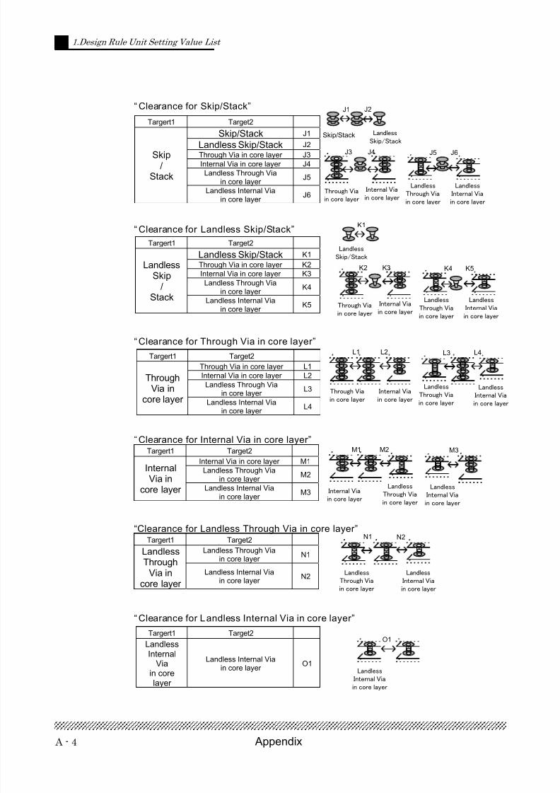
7/27/2019 Design Library Master Training_cr
http://slidepdf.com/reader/full/design-library-master-trainingcr 85/89
Appendix A - 4
1.Design Rule Unit Setting Value List
“ Clearance for Skip/Stack”
“ Clearance for Landless Skip/Stack”
“ Clearance for Through Via in core layer”
“ Clearance for Internal Via in core layer”
“Clearance for Landless Through Via in core layer”
“ Clearance for Landless Internal Via in core layer”
Targert1 Target2
Skip/Stack J1
Landless Skip/Stack J2
Through Via in core layer J3
Internal Via in core layer J4
Landless Through Viain core layer
J5
Skip/
Stack
Landless Internal Viain core layer
J6
Targert1 Target2
Landless Skip/Stack K1
Through Via in core layer K2
Internal Via in core layer K3
Landless Through Viain core layer
K4
Landless
Skip/
Stack Landless Internal Viain core layer
K5
Targert1 Target2
Through Via in core layer L1
Internal Via in core layer L2
Landless Through Viain core layer
L3
ThroughVia in
core layer Landless Internal Viain core layer
L4
Targert1 Target2
Internal Via in core layer M1
Landless Through Viain core layer
M2InternalVia in
core layer Landless Internal Viain core layer
M3
Targert1 Target2
Landless Through Viain core layer N1LandlessThrough
Via incore layer
Landless Internal Viain core layer
N2
Targert1 Target2
LandlessInternal
Viain corelayer
Landless Internal Viain core layer
O1
Through Via
in core layer
J2J1
J3
Internal Via
in core layer
J4 J6J5
Landless
Internal Via
in core layer
Landless
Through Via
in core layer
Landless
Skip/StackSkip/Stack
K1
K2 K3 K5K4
Through Via
in core layer
Internal Via
in core layer
Landless
Internal Via
in core layer
Landless
Through Via
in core layer
Landless
Skip/Stack
L1 L2 L4L3
Through Via
in core layer
Internal Via
in core layer
Landless
Internal Via
in core layer
Landless
Through Via
in core layer
M1 M2 M3
Internal Via
in core layer
Landless
Internal Via
in core layer
Landless
Through Via
in core layer
N1 N2
Landless
Internal Via
in core layer
Landless
Through Via
in core layer
O1
Landless
Internal Via
in core layer
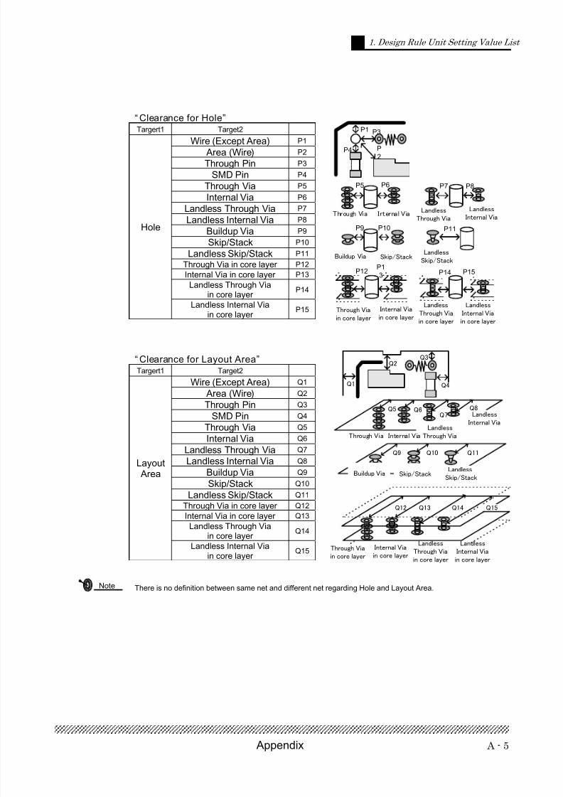
7/27/2019 Design Library Master Training_cr
http://slidepdf.com/reader/full/design-library-master-trainingcr 86/89
A - 5 Appendix
1. Design Rule Unit Setting Value List
“ Clearance for Hole”Targert1 Target2
Wire (Except Area) P1
Area (Wire) P2
Through Pin P3
SMD Pin P4
Through Via P5
Internal Via P6
Landless Through Via P7
Landless Internal Via P8
Buildup Via P9
Skip/Stack P10
Landless Skip/Stack P11
Through Via in core layer P12
Internal Via in core layer P13
Landless Through Viain core layer
P14
Hole
Landless Internal Viain core layer
P15
“ Clearance for Layout Area”Targert1 Target2
Wire (Except Area) Q1
Area (Wire) Q2
Through Pin Q3
SMD Pin Q4Through Via Q5
Internal Via Q6
Landless Through Via Q7
Landless Internal Via Q8
Buildup Via Q9
Skip/Stack Q10
Landless Skip/Stack Q11
Through Via in core layer Q12
Internal Via in core layer Q13
Landless Through Viain core layer
Q14
Layout Area
Landless Internal Via
in core layer
Q15
There is no definition between same net and different net regarding Hole and Layout Area.
P3
P
2
P1
P8P7P6P5
P12P1
3P15P14
P11P10P9
P4
Landless
Through Via
Landless
Internal ViaThrough Via Internal Via
Skip/StackLandless
Skip/StackBuildup Via
Internal Via
in core layer
Landless
Internal Via
in core layer
Landless
Through Via
in core layer
Through Via
in core layer
Q3
Q4Q1
Q8Q7
Q6Q5
Q2
Q11Q10Q9
Q12 Q13 Q14 Q15
Landless
Through Via
Landless
Internal Via
Through Via Internal Via
Skip/StackLandless
Skip/StackBuildup Via
Internal Via
in core layer
Landless
Internal Via
in core layer
Landless
Through Via
in core layer
Through Via
in core layer
Note
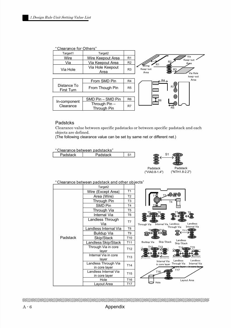
7/27/2019 Design Library Master Training_cr
http://slidepdf.com/reader/full/design-library-master-trainingcr 87/89
Appendix A - 6
1.Design Rule Unit Setting Value List
“ Clearance for Others”Targert1 Target2
Wire Wire Keepout Area R1
Via Via Keepout Area R2
Via HoleVia Hole Keepout
AreaR3
From SMD Pin R4
Distance ToFirst Turn
From Though Pin R5
SMD Pin – SMD Pin R6In-component
ClearanceThrough Pin –Through Pin
R7
PadstcksClearance value between specific padstacks or between specific padstack and eachobjects are defined.(The following clearance value can be set by same net or different net.)
“ Clearance between padstacks”
Padstack Padstack S1
“ Clearance between padstack and other ob jects”Target2
Wire (Except Area) T1
Area (Wire) T2
Through Pin T3
SMD Pin T4
Through Via T5
Internal Via T6
Landless ThroughVia
T7
Landless Internal Via T8Buildup Via T9
Skip/Stack T10
Landless Skip/Stack T11
Through Via in corelayer
T12
Internal Via in corelayer
T13
Landless Through Viain core layer
T14
Landless Internal Viain core layer
T15
Hole T16
Padstack
Layout Area T17
Wiring
Keep-out
Area
ViaKeep-out
Area
Via Hole
keep-out
Area
R1R2
R3
R5
R7
R4
R6
Padstack
("NTH1.8-2.2")
Padstack
("VIA0.8-1.4")
S1
T8
Landless Through Via
Landless Internal Via
T7 T6 T5
Through Via Internal Via
T12
Internal Via in core layer
T13 T15 T14
Landless Internal Via in core layer
Landless Through Via in core layer
T11
Landless Skip/Stack
T10
Buildup Via Skip/Stack
T9
T17 T16
T3 T1
T2
Hole Layout Area
T4

7/27/2019 Design Library Master Training_cr
http://slidepdf.com/reader/full/design-library-master-trainingcr 88/89
Zuken Inc.
Master Training <PCB Design Library> Serial ID C2B1001E

7/27/2019 Design Library Master Training_cr
http://slidepdf.com/reader/full/design-library-master-trainingcr 89/89


![Master Thesis - Benjamin Speckmann [PDF Library]](https://img.pdfslide.net/doc/110x75/5477ddad5806b506198b4680/master-thesis-benjamin-speckmann-pdf-library.jpg)