Embed Size (px)
Citation preview

DESIGN OF RF POWER AMPLIFIER WITH DIFFERENT BIASING BASED ON
GREEN DESIGN TECHNIQUE
MUHAMMAD ASHRAF BIN SABRI
This report is submitted in partial of requirements for the award of
Bachelor Degree of Electronics Engineering (Electronic Telecommunication) With
Honours.
Faculty of Electronics and Computer Engineering
UNIVERSITI TEKNIKAL MALAYSIA MELAKA
JUNE 2016

UNIVERSTI TEKNIKAL MALA YSlA MELAKA FAKULTI KEJURUTERAAN ELEKTRONIK DAN KEJURUTERAAN KOMPUTER
BORA 'G PENGESAHAN STATUS LAPORAN
PROJEK SARJANA MUDA II
Tajuk Projek DESIGN OF RF POWER AMPLIFIER WITH DIFFERENT BIASING BASED ON GREEN DESIGN TECHNIQUE
Sesi Pengajian 5 I 6
Saya MUHAMMAD ASHRAF BIN SABRJ mengaku membenarkan Laporan Projek Sarjana Muda ini disimpan di Perpustakaan dengan syarat-syarat kegunaan seperti berikut:
I. Laporan adalah hakmilik Universiti Teknikal Malaysia Melaka.
2. Perpustakaan dibenarkan membuat salinan untuk tujuan pengajian sahaja.
3. Perpustakaan dibenarkan membuat salinan laporan ini sebagai bahan pertukaran antara institusi
pengajian tinggi .
4. Sila tandakan ( ..J ) :
D SULIT*
D TERHAD**
EJ TIDAK TERHAD
(T ANDA T ANGAN PENULIS)
Tarikh :2. / r, / I 6
*(Mengandungi maklumat yang berdarjah keselamatan atau kepentingan Malaysia seperti yang termaktub di dalam AKT A RAHSIA RASMI 1972)
**(Mengandungi maklumat terhad yang telah ditentukan oleh organisasilbadan di mana penyelidikan dijalankan)

lll
"I hereby declare that the work in this project is my own except for summaries and quotations which have been duly acknowledge."
Signature
Author
Date
•• ~ HO
: MUHAMMAD ASHRAF BIN SABRI
,_ 0 /~· /t I,

IV
"I acknowledge that I have read this report and in my opinion this report is sufficient in term of scope and quality for the award of B elor of Electronic Engineering
(Electronic Telecommunic with Honours."
Signature
Supervisor' s Name
Date : ... ... .. . :~ .q 0./t.~ ................. .

v
To my beloved mother, father and family

VI
ACKNOWLEDGEMENT
Assalamualaikum W.B.T
Alhamdulillah. Firstly, I want to praise, to Allah S.W.T because give me strength
to finish this report successfully. On this occasion, I want to thank to our project
supervisor Mr. Azahari Bin Salleh for his cooperation and encouragement in preparing
this report, either directly or otherwise. Without him, I cannot finish up the project and
report successfully and he also supported me to solve any problem during fmished this
project and report.
Secondly, I also want to thank all lectures of Universiti Teknikal Malaysia
Melaka especially to lecturer in Faculty Electronic and Computer Engineering (FKEKK)
for their ideas, knowledge, guidance and encouragement that help I fmished this report
completely. Besides that, I also want to thank my friends and also to my beloved family
that help to provide facilities , information, produced brilliant ideas and give support for
me to complete this report for this final semester.
Finally, my grateful thank goes to all of them who help me a lot. A big
contribution from those involved during report preparing. During the final year project,
the lecturers and technicians introduced and deliver all the basic knowledge about
engineering and electronics. Good appreciation to instructors and technicians in assisting
us for final year project.
Thank you.

VII
ABSTRACT
Nowadays, the development of low-cost, low-power radio frequency (RF) for a
base station application grows rapidly. The high power consumption of a base station is
caused by poor efficiency in RF power amplifier design. The project is based on RF
power amplifiers and green design technique that have been used in a variety of
applications for example are the wireless communication. Green design technique is
used to improve the performance of power amplifier and thus lower the power
consumption. The main purpose of an RF power amplifier is to boost radio signal to a
sufficient power level for transmission through the air interface from transmitter to
receiver. The most important parameter is the gain, return loss, efficiency, output power
and power consumption of the amplifier. This parameter is to ensure the design
amplifier can work at the desired frequency. The aim of this project is to design and
compare a power amplifier for base station application at 5.8 GHz operating frequency
that using two different biasing network, with a power amplifier gain above I 0 dB and
required to achieve low power consumption. Advance Design System (ADS) software is
used in power amplifier design simulation. At the end of the project, it shows that
between two biasing, the passive biasing is better compared to active biasing since it
produce gain of 10.857 dB and low power consumption which is 0.986 W. The output
power and return loss achieved are 20.858 dBm and -44.099 dB while the Power Added
Efficiency (PAE) is 24.54 %.

VIII
ABSTRAK
Pada masa kini , pembangunan peranti frekuensi radio (RF) untuk aplikasi stesen
pangkalan berkos rendah dan berkuasa rendah berkembang pesat. Penggunaan kuasa
yang tinggi oleh stesen pangkalan adalah disebabkan oleh kecekapan penguat kuasa
(RF) yang kurang. Projek ini adalah berdasarkan kepada penguat kuasa RF dan teknik
reka bentuk teknologi hijau yang telah digunakan dalam pelbagai aplikasi contohnya
ialah komunikasi tanpa wayar. Teknik reka bentuk teknologi hijau digunakan untuk
meningkatkan prestasi penguat kuasa dan sekaligus mengurangkan penggunaan kuasa.
Tujuan utama penguat kuasa RF adalah untuk meningkatkan isyarat radio ke tahap kuasa
yang mencukupi untuk penghantaran isyarat melalui udara dari penghantar kepada
penerima. Parameter yang paling penting adalah gandaan, kehilangan pulangan,
kecekapan, kuasa keluaran dan penggunaan kuasa. Parameter ini adalah untuk
memastikan reka bentuk penguat boleh bekerja pada frekuensi yang dikehendaki. Tujuan
projek ini adalah untuk mereka bentuk dan membandingkan penguat kuasa bagi aplikasi
stesen pangkalan pada frekuensi 5.8 GHz yang menggunakan dua rangkaian pincangan
yang berbeza, dengan gandaan penguat kuasa melebihi 1 0 dB dan diperlukan untuk
mencapai penggunaan tenaga yang rendah. Perisisan Advance Design System (A DS)
digunakan dalam simulasi reka bentuk penguat kuasa. Pada akhir projek ini , ia
menunjukkan bahawa antara dua pincangan, pincangan pasif adalah lebih baik
berbanding pincangan aktif kerana ia menghasilkan gandaan sebanyak 10.857 dB dan
penggunaan kuasa yang rendah iaitu 0.986 W. Kuasa keluaran dan kehilangan pulangan
dicapai adalah 20.858 dBm dan -44.099 dB manakala PAE adalah 24.54%.

IX
TABLE OF CONTENT
CHAPTER CONTENT PAGE
PROJECT TOPIC
BORANG PENGESAHAN STATUS LAPORAN ii
DECLARATION iii
DEDICATION v
ACKNOWLEDGEMENT vi
ABSTRACT vii
ABSTRAK viii
TABLE OF CONTENT ix
LIST OF TABLES xii
LIST OF FIGURES xiii
LIST OF ABBREVIATIONS XV
LIST OF SYMBOLS xvi
LIST OF APPENDICES xviii
1 INTRODUCTION
1.1 Background
1.2 Problem Statement 3
1.3 Objective of Project 5
1.4 Scope of Project 5
1.5 Thesis Outline 6
2 LITERATURE REVIEW

X
2.1 Introduction 8
2.2 Reviews of Power Amplifier 10
2.3 Power Amplifier Parameter 12
2.3.1 Stability 12
2.3.2 Linearity 13
2.3 .3 Efficiency 14
2.3.4 Output Power 15
2.3.5 1-dB Compression Point (P 1-dB) 17
2.3.6 Gain 17
2.3.7 lntermodulation Distortion (IMD) 18
2.4 Bias Network 18
2.4.1 Passive Bias 19
2.4.2 Voltage Divider Bias 20
2.4.3 Active Bias 22
2.4.4 Current Mirror Bias 23
2.5 Review of Previous Paper 24
2.5.1 Overall Summary of Previous Paper 28
3 METHODOLOGY
3.1 Flowchart of Project Methodology 30
3.2 Design Methodology 33
3.2.1 Power Amplifier Design 33
3.2.2 Specification of Power Amplifier 34
3.2.3 Advanced Design System 35
3.2.4 Selection of Transistor 36
3.2.4.1 Transistor Analysis and Theory 37
3.2.5 Stability 38
3.2.6 Biasing 40
3.2.7 Input and Output Matching Network 43
3.2.8 Optimization 44

XI
4 RESULT AND DISCUSSIONS
4.1 Basic Power Amplifier Design 45
4.1.1 Biasing Point Simulation 46
4.1.2 Transistor Parameter Simulation 47
4.1.2.1 Stability and S -Parameter 47
4.1.3 Two Port Network 50
4.1.4 Maximum Gain (Conjugate Matching) 51
4.1.5 Power Added Efficiency 53
4.2 Matching Network Design 54
4.2.1 Microstrip Line Implementation 55
4.3 Biasing Network Simulation 58
4.3.1 Passive Biasing 58
4.3.2 Active Biasing 60
4.4 Single Stage Amplifier Design 62
4.4.1 Single Stage Power Amplifier with Passive Biasing 63
4.4.1.1 S -Parameter Analysis 64
4.4.1 .2 One Tone Simulation Analysis 65
4.4.2 Single Stage Power Amplifier with Active Biasing 67
4.4.2.1 S -Parameter Analysis 68
4.4.2.2 One Tone Simulation Analysis 69
4.5 Analysis Summary for Biasing Comparison 71
5 CONCLUSION AND FUTURE WORK
5.1 Conclusion 73
5.2 Future Work 75
REFERENCES 76
APPENDICES 79

XII
LISTS OF TABLE
TABLE NO. CONTENT PAGE
2.1 Overall Summarized Parameter for Reviewed Paper 2
3.1 The specifications of the power amplifier design 2
4.1 The S-parameter value of the transistor 3
4.2 Input and Output Matching 3
4.3 Summarized results for the comparison of biasing networks 6

X III
LISTS OF FIGURES
CHAPTER CONTENT PAGE
2.1 Schematic diagram of a class A amplifier 11
2.2 Passive bias circuits for MESFET 20
2.3 Voltage Divider Bias configuration 21
2.4 Active Bias configuration 22
2.5 Current Mirror Bias configuration 23
2.6 Schematic diagram of RF amplifier module 27
3.1 Flowchart of project design 31
3.2 Basic Amplifier Circuit 34
3.3 Flowchart for simulation process 36
3.4 S- Parameter simulation circuit 39
3.5 Circuit for DC bias point by using FET curve tracer 40
4.1 Transistor IV curve 47
4.2 Stability Factor, K 49
4.3 Noise Figure 50
4.4 Smith Chart of Source and load reflection Coefficient 53
4.5 Power Added Efficiency 54
4.6 Schematic for Input and Output Matching for Single Stub 58
4.7 Passive biasing design 60
4.8 Active biasing design 62
4.9 Single Stage Amplifier with Passive Biasing 63
4.10 S-Parameter Power Amplifier with Passive Biasing 65
4.11 Output Power Simulation Passive Biasing 66

XIV
4.12 PAE Simulation Passive Biasing 67
4.13 Single Stage Amplifier with Active Biasing 68
4.14 S-Parameter Power Amplifier with Active Biasing 69
4.15 Output Power Simulation Activeive Biasing 70
4.16 PAE Simulation Active Biasing 71
AC
ADS
BJT
BW
DC
EDA
EM
GA
GaAsFET
Gmax
GP
GT
IEEE
IMD
MAG
MMDS
MOS
PA
PAE
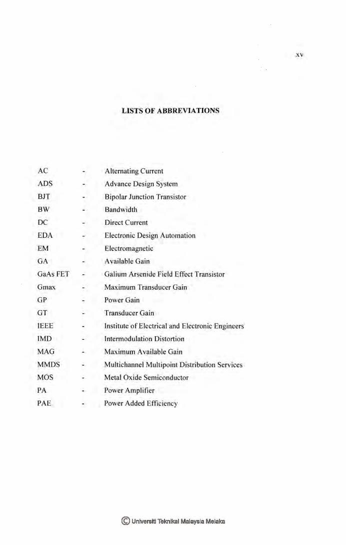
LISTS OF ABBREVIATIONS
Alternating Current
Advance Design System
Bipolar Junction Transistor
Bandwidth
Direct Current
Electronic Design Automation
Electromagnetic
Available Gain
Galium Arsenide Field Effect Transistor
Maximum Transducer Gain
Power Gain
Transducer Gain
Institute of Electrical and Electronic Engineers
Interrnodulation Distortion
Maximum Available Gain
Multichannel Multipoint Distribution Services
Metal Oxide Semiconductor
Power Amplifier
Power Added Efficiency
X V

XVI
LISTS OF SYMBOLS
c Capacitor
d Thickness
dB Decibel
dBm MiliDecibels
GHz Gigahertz
K Rollet's Stability Factor
rnA Miliampere
Mbit/s - Megabit per second
Mm Milimeter
mW MiliWatt
MW MegaWatt
p Power
R Resistance
s Scattering
511 Input Return Loss
522 Output Return Loss
521 Gain
512 Insertion Loss
v Voltage
z Impedance
0 Degree
Er Dielectric constant
I} Efficiency
n Ohm

n r 'A
Pi
Reflection Coefficient
Wavelength
XV II

XV III
LISTS OF APPENDICES
APPENDIX TITLE PAGE
A Transistor Datasheet (Agilent ATF 54143) 79

CHAPTER 1
INTRODUCTION
In this chapter, an introduction with motivations and objectives of this project are
present. Thus, this chapter focuses on the project background, problem statements,
project objectives, scope of work and thesis outline.
1.1 Project Background
The green technology definition, in simple words, it means the technology,
which is environmentally friendly, developed and used in such a way so that it doesn ' t
disturb our environment and conserves natural resources . We may also hear green

2
technology being referred to as environmental technology and clean technology. In the
stages of its development, the future only promises to bring bigger and better things in
this field. It will in fact be a necessity of the future . A radio frequency power
amplifier (RF power amplifier) is a type of electronic amplifier that converts a low
power radio-frequency signal into a higher power signal. Typically, RF power amplifiers
drive the antenna of a transmitter. Biasing in electronics is the method of establishing
predetermined voltages or currents at various points of an electronic circuit for the
purpose of establishing proper operating conditions in electronic components.
Radio Frequency (RF) power amplifiers are commonly used in wireless
communication devices such as cellular phone, radios and wireless modem amplify and
transmit (RF) signals. Radio frequency transmission of an electrical signal requires
corresponding power amplification for the intended transmission range. RF signals
typically have a broad frequency spectrum from several Megahertz (MHz) to tens of
Gigahertz (GHz) and higher. A power amplifier amplifies a radio frequency signal at the
output of a transmitter prior to transmission in a small-size communication device. A
typical radio transmitter uses an (RF) power amplifier to amplify outbound signals for
transmission by an antenna. RF power amplifiers are generally designated to provide
maximum efficiency at the maximal output power. Within the amplifier assemblies are
typically the plural printed circuit boards on which components that process the RF
signals are mounted . Typically, an RF power amplifier consists of an integrated circuit
chip having the transistors and other circuitry associated with the amplifier and a number
of off-chip components that filter the signal or provide impedance matching at a
particular operating frequency. RF signals are transmitted between the various
processing components.
The main purpose of this pr:oject is to design and compare different types of
biasing network for RF power amplifier for base station application which operating at
5.8 GHz. In this project a 5.8 GHz frequency will be used . Important parameters for RF

3
power amplifier are Power Added Efficiency (PAE), gain, output power, return loss and
DC power consumption.
1.2 Problem statement
In the recent years, wireless devices and mobile communication systems have
increasingly become very popular. Currently, 3% of the world-wide energy is consumed
by the (Information and Communication Technology) JCT infrastructure, which causes
about 2% of the world-wide C02 emissions. Today, more than four billion people in the
world have access to the mobile phones. The overall energy consumption of mobile
devices seems to be more than those of base-stations. Good environmental control and
less energy consumption will contribute to slow down the abnormal temperature
variation. Recently, green technologies that can reduce energy consumption and carbon
dioxide emission and reuse the resources have been attracting many people. Especially,
green Information Communication Technology (ICT) has been studied widely to
achieve high Energy Efficiency (EE), and to resolve the conflict between high demands
of Quality-of-Service (QoS) and energy saving [1].
Base stations represent the main contributor to the energy consumption of a
mobile cellular network. Since the traffic load on mobile networks significantly varies
during a working or weekend day, it is important to quantify the influence of these
variations on the base station power consumption. To reduce the energy consumption of
cellular networks, precise knowledge about base station energy consumption and the
influence of the traffic load on the instantaneous base station power consumption can be
of great importance. Generally, it is assumed that the traffic load variations have a small
influence on the power consumption of the base station [2).

4
Inside a base station, there is an RF power amplifier. The level of performance of
RF power amplifier is determined from the bias points of an RF power amplifier. Based
on the bias points of power amplifier approaches, it can evaluate value for output power,
efficiency, linearity, and other parameters of power amplifier.
Without a power amplifier in a system, the receiver of a system cannot receive
the full information from the transmit signal. The information signals that transmit by,
the transmitter will attenuate itself and the information which is not having the full info
that transmitted to the receiver also known as a loss signal. The signal can attenuate
itself because of its natural consequence of signal transmission over long distances.
Thus, the power amplifier can be concluded that it acts as a booster for a signal before
being transmitted to ensure the receiver to receive all the signal information without any
loss.
The design of RF power amplifier might have two major problems. The first
problem is the lower breakdown voltage due to scaling down in technology that restricts
the maximum output power and second problem is the reduced transconductance of
transistors, leading to inferior power gain and poorer efficiency that leads to high power
consumption.In order to solve this problem, there are many methods and technique
being established and one of them is green design technique. For the green design
technique, there are many method uses to achieve low power consumption. Therefore
the purpose of this project is to design an RF power amplifier based on green design
technique in order solve the high power consumption problem of RF power amplifier
design by using different biasing network. In this project; the biasing network will be
manipulated in order to achieve high efficiency [I].

5
1.3 Project Objective
The objective of the project is to design a 5.8 GHz green RF power amplifier
with different type of biasing network. The simulation power amplifier is done by
comparing between two types of biasing network by using the Advance Design System
(ADS) software.
1.4 Scope of Work
The scope of works for this project is to design an RF power amplifier for a base
station application which operate at the frequency of 5.8 GHz by using two different
types of biasing networks.
In order to achieve the objective of this project, below are the following scopes
that will be covered:
a) To study the concept of power amplifier and green technique
b) All parts of the design are operating at 5.8 GHz
c) The power amplifier will be simulated by using the Advance Design
System (ADS).
d) Selecting the suitable transistor to be used for the design
e) The analysis of the power amplifier will be made based on parameter
such as stability, PAE, DC power consumption, return loss, gain, and
output power.
f) Compare the performance of power amplifier with different biasing
network.

6
g) Compare the calculated value and simulation value of the parameter state
above.
1.5 Thesis Outline
This thesis is a document that delivers the ideas generated and the concept
applied . In chapter one briefly introduces the overall of the project. The introduction
consists of the project background, objective, problem statement, scopes and thesis
outline.
Meanwhile, chapter two contains the literature review of the power amplifier and
green technique. It discusses the researches done upon the related project, and data
obtained through journals, books, magazine, and internet.
Chapter three briefing more about power amplifier that includes the type of
matching networks, a type of transistor, types of biasing network and more details on the
power amplifier design.
Chapter four describes the methodology of the project, which includes the
project flow and its functional block diagram. It also discusses the methods used for the
project such as software applied, hardware and the reasons behind it.


![RF Module Design - [Chapter 6] Power Amplifier](https://img.pdfslide.net/doc/110x75/55cf0487bb61eb052d8b4596/rf-module-design-chapter-6-power-amplifier.jpg)