Embed Size (px)
Citation preview
DesignCon 2015
IBIS-AMI Modeling and Simulation
of 56G PAM4 Link Systems
Hongtao Zhang, Xilinx Inc.
Fangyi Rao, Keysight Technologies
Xiaoqing Dong, Huawei Technologies
Geoff Zhang, Xilinx Inc.
Abstract
PAM4 signaling has been proposed and discussed at various standard bodies for several years.
With limited or even no experience with high speed link systems using PAM4, system engineers
need to rely on end-to-end system level simulations. On the other hand, the IBIS-AMI standard
provides interoperability, SerDes IP protection, excellent accuracy, and high throughput for link
simulations. Unfortunately, today IBIS-AMI only supports NRZ signaling. Modifications are
necessary in order to support PAM4.
In this paper an extension of IBIS-AMI for PAM4 signaling is discussed. Details of required
and/or suggested changes for both TX and RX are presented. The feasibility of the proposed
approach is demonstrated by providing case studies of a simulation flow. Simulation results of a
56G PAM4 LR link using an IBIS-AMI model on a commercial EDA tool are presented. It is
hoped that formal specifications will soon be adopted for IBIS-AMI for modeling PAM4
signaling.
Authors Biography
Hongtao Zhang received his Ph.D. degree in Electrical and Computer Engineering from
University of California, San Diego in 2006. He joined Xilinx in 2013 as a staff SerDes architect,
developing SerDes architectures for both NRZ and PAM4 signaling. From 2010 to 2013, he was
with SerDes design team at Oracle Corporation, where he worked on circuit design and
architecture modeling. Prior to that, he worked on SerDes characterization at Texas Instruments,
Dallas. His current interests are SerDes architecture development and simulation, analog and
digital circuit implementation and optimization, and system level modeling.
Fangyi Rao received his Ph.D. degree in theoretical physics from Northwestern University in
1997. He joined Agilent/Keysight EEsof in 2006 and works on Analog/RF and SI simulation
technologies in ADS. From 2003 to 2006 he was with Cadence Design Systems, where he
developed SpectreRF Harmonic Balance technology and perturbation analysis of nonlinear
circuits. Prior to 2003 he worked in the areas of EM simulation, nonlinear device modeling, and
medical imaging.
Xiaoqing Dong joined Huawei Technologies in 2006 as a signal integrity research engineer. She
has been working on high speed link SI simulation and measurement. She received her bachelor
and master degrees in Communications and Information System from Harbin Institute of
Technology, China, for research in Information and Communication Engineering.
Geoff Zhang received his Ph.D. in 1997 in Microwave Engineering and Signal Processing from
Iowa State University. He joined Xilinx SerDes Technology Group in 2013 to lead the SerDes
architecture and modeling group. Since 1997 Geoff has worked at Xilinx, Huawei, LSI, Agere
Systems, Lucent, and Texas Instruments. His current work involves SerDes architecture
modeling and high speed system level analysis.
1. Introduction
This paper introduces Input/Output Buffer Information Specification Algorithmic Model
Interface (IBIS-AMI) modeling and simulation of PAM4 (4 level Pulse Amplitude Modulation)
signaling for high speed serial link systems. As data rate goes beyond 40Gbps, PAM4 signaling
is gaining traction, especially for backplane applications. While System engineers have been
designing systems using NRZ for more than a decade, not many have experience with PAM4.
This makes system simulation indispensable in PAM4 link design, budgeting and optimization.
To accurately simulate a serial link, it is critical to model the link channel and SerDes (or other
active component, such as repeaters) accurately, besides setting up system parameters like jitter
and noise. Inside the SerDes we need to model the behavior of feed-forward-equalization (FFE),
continuous-time-linear-equalization (CTLE), decision-feedback-equalization (DFE) and clock-
data-recovery (CDR), both hardware and adaptations. Impairments and design trade-offs will
also have to be represented inside the model. However, such information is typically proprietary
for SerDes vendors, thus unavailable to system engineers. This poses a challenge to the system
simulation.
Another challenge is model interoperability. As a third-party SerDes IP is usually required in
many application scenarios, there is a need to establish a common interface standard for
interoperability simulation. Still another challenge is simulation speed. As most design specs are
defined at bit-error-ratio (BER) of 1e-12 or lower, designers need to run millions of bits in order
to predict a link performance at very low BER levels.
Above challenges are addressed by the IBIS-AMI standard. By defining a common SerDes
model interface, the standard allows SerDes vendors to encapsulate SerDes behaviors in model
executables without exposing their IP. The models can be used by system designers to perform
end-to-end link simulations. Furthermore, in AMI simulations analog channels are assumed to be
linear-time-invariant (LTI) and can be represented by impulse responses. The highly efficient
convolution method can be applied to calculating signal waveforms at channel outputs. As a
result, millions of bits can be simulated in minutes, allowing accurate predictions of link
performance at low BER with good confidence.
This paper introduces a case study running the PAM4 56G AMI model in a commercial
Electronic Design Automation (EDA) simulator. The current AMI standard only supports NRZ
signaling as it assumes that the transmitter (TX) input signal has two levels and the receiver (RX)
slicer reference is at 0V. To support PAM4, both assumptions must be modified. In particular,
RX may adjust slicer references for different signal levels on the fly, and such adjustments need
to be reflected in eye and BER calculations.
In this paper we propose an extension to AMI for PAM4 modeling and simulation. For TX, the
PAM4 input signal has four levels for any coding schemes. For RX, besides the output waveform
and clock ticks in NRZ, the AMI_GetWave function also returns instantaneous slicer reference
values (both error and data slicers are applicable). They are used by the simulator to align the RX
output signal when calculating eye diagram and BER. We demonstrate feasibility and
interoperability of the proposed approach by presenting details of modification, the simulation
flow, and case study results of running a 56G PAM4 AMI model on a commercial EDA tool.
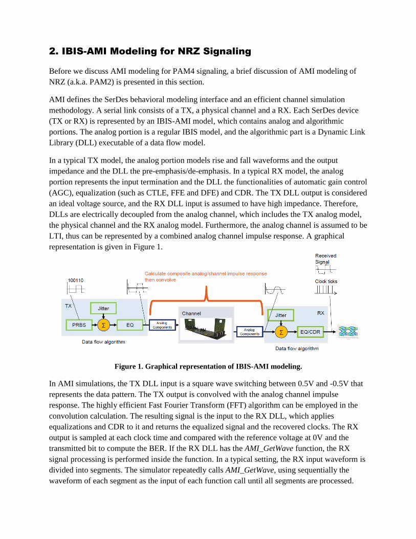
2. IBIS-AMI Modeling for NRZ Signaling
Before we discuss AMI modeling for PAM4 signaling, a brief discussion of AMI modeling of
NRZ (a.k.a. PAM2) is presented in this section.
AMI defines the SerDes behavioral modeling interface and an efficient channel simulation
methodology. A serial link consists of a TX, a physical channel and a RX. Each SerDes device
(TX or RX) is represented by an IBIS-AMI model, which contains analog and algorithmic
portions. The analog portion is a regular IBIS model, and the algorithmic part is a Dynamic Link
Library (DLL) executable of a data flow model.
In a typical TX model, the analog portion models rise and fall waveforms and the output
impedance and the DLL the pre-emphasis/de-emphasis. In a typical RX model, the analog
portion represents the input termination and the DLL the functionalities of automatic gain control
(AGC), equalization (such as CTLE, FFE and DFE) and CDR. The TX DLL output is considered
an ideal voltage source, and the RX DLL input is assumed to have high impedance. Therefore,
DLLs are electrically decoupled from the analog channel, which includes the TX analog model,
the physical channel and the RX analog model. Furthermore, the analog channel is assumed to be
LTI, thus can be represented by a combined analog channel impulse response. A graphical
representation is given in Figure 1.
Figure 1. Graphical representation of IBIS-AMI modeling.
In AMI simulations, the TX DLL input is a square wave switching between 0.5V and -0.5V that
represents the data pattern. The TX output is convolved with the analog channel impulse
response. The highly efficient Fast Fourier Transform (FFT) algorithm can be employed in the
convolution calculation. The resulting signal is the input to the RX DLL, which applies
equalizations and CDR to it and returns the equalized signal and the recovered clocks. The RX
output is sampled at each clock time and compared with the reference voltage at 0V and the
transmitted bit to compute the BER. If the RX DLL has the AMI_GetWave function, the RX
signal processing is performed inside the function. In a typical setting, the RX input waveform is
divided into segments. The simulator repeatedly calls AMI_GetWave, using sequentially the
waveform of each segment as the input of each function call until all segments are processed.
3. Brief Introduction to PAM4 Signaling
400G links will be the answer to the requirement of next generation networking
bandwidth. Single lane data rate will reach 50G+. Both OIF CEI-56G study group and IEEE
400G study group are currently working on 56G specifications. Based on straw polls at OIF it
seems PAM4 signaling is an enabling technology to implement 400G, at least for medium reach
(MR) and long reach (LR) applications.
Unlike NRZ, PAM4 signaling is still new to most engineers working on high speed serial link
systems. In this section we provide a brief introduction to PAM4 signaling so that basic ideas
and concepts are established. Details of PAM4 SerDes architecture and design are beyond the
scope of this paper.
3.1 What is PAM4?
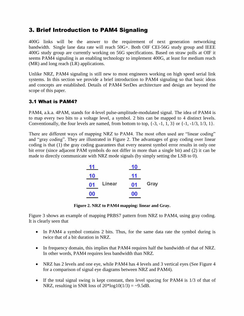
PAM4, a.k.a. 4PAM, stands for 4-level pulse-amplitude-modulated signal. The idea of PAM4 is
to map every two bits to a voltage level, a symbol. 2 bits can be mapped to 4 distinct levels.
Conventionally, the four levels are named, from bottom to top, {-3, -1, 1, 3} or {-1, -1/3, 1/3, 1}.
There are different ways of mapping NRZ to PAM4. The most often used are “linear coding”
and “gray coding”. They are illustrated in Figure 2. The advantages of gray coding over linear
coding is that (1) the gray coding guarantees that every nearest symbol error results in only one
bit error (since adjacent PAM symbols do not differ in more than a single bit) and (2) it can be
made to directly communicate with NRZ mode signals (by simply setting the LSB to 0).
Figure 2. NRZ to PAM4 mapping: linear and Gray.
Figure 3 shows an example of mapping PRBS7 pattern from NRZ to PAM4, using gray coding.
It is clearly seen that
In PAM4 a symbol contains 2 bits. Thus, for the same data rate the symbol during is
twice that of a bit duration in NRZ.
In frequency domain, this implies that PAM4 requires half the bandwidth of that of NRZ.
In other words, PAM4 requires less bandwidth than NRZ.
NRZ has 2 levels and one eye, while PAM4 has 4 levels and 3 vertical eyes (See Figure 4
for a comparison of signal eye diagrams between NRZ and PAM4).
If the total signal swing is kept constant, then level spacing for PAM4 is 1/3 of that of
NRZ, resulting in SNR loss of 20*log10(1/3) = ~9.5dB.
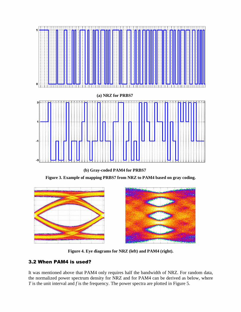
(a) NRZ for PRBS7
(b) Gray-coded PAM4 for PRBS7
Figure 3. Example of mapping PRBS7 from NRZ to PAM4 based on gray coding.
Figure 4. Eye diagrams for NRZ (left) and PAM4 (right).
3.2 When PAM4 is used?
It was mentioned above that PAM4 only requires half the bandwidth of NRZ. For random data,
the normalized power spectrum density for NRZ and for PAM4 can be derived as below, where
T is the unit interval and f is the frequency. The power spectra are plotted in Figure 5.
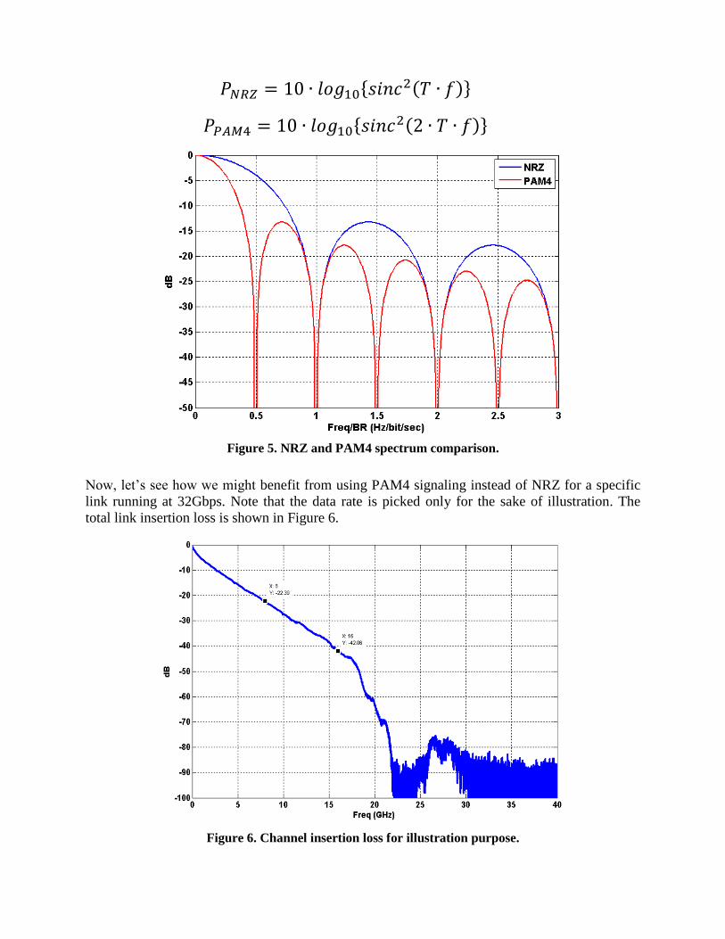
𝑃𝑁𝑅𝑍 = 10 ∙ 𝑙𝑜𝑔10{𝑠𝑖𝑛𝑐2(𝑇 ∙ 𝑓)}
𝑃𝑃𝐴𝑀4 = 10 ∙ 𝑙𝑜𝑔10{𝑠𝑖𝑛𝑐2(2 ∙ 𝑇 ∙ 𝑓)}
Figure 5. NRZ and PAM4 spectrum comparison.
Now, let’s see how we might benefit from using PAM4 signaling instead of NRZ for a specific
link running at 32Gbps. Note that the data rate is picked only for the sake of illustration. The
total link insertion loss is shown in Figure 6.
Figure 6. Channel insertion loss for illustration purpose.
The Nyquist frequency for NRZ is 16GHz, while for PAM4 it is 8GHz. The insertion losses at
the two frequencies are 42.1dB and 22.4dB, respectively. The net difference is therefore 42.1-
22.4 = 19.7dB, enough to compensate for the 9.5dB loss in SNR due to reduced signal amplitude
in PAM4 signaling. Consequently, PAM4 signaling could be a better choice in this regard.
On the other hand, 42dB loss at the Nyquist frequency is a little too excessive for a NRZ link
without resorting to FEC for BER<1e-15. As a result, it could be justified that for this link to run
at 32Gbps, PAM4 is most likely a better candidate than NRZ. Note that implementation cost and
compatibility could favor NRZ; this topic is outside the scope of this paper.
3.3 How is PAM4 signal detected?
To reduce channel loss induced ISI and to ensure signal is sampled at the center of the eye, a
PAM4 SerDes employs equalization (transmitter de-emphasis, receiver equalization, such as
CTLE, FFE, and DFE), and timing recovery.
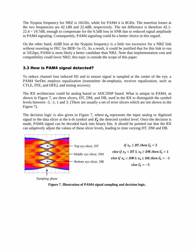
The RX architecture could be analog based or ADC/DSP based. What is unique in PAM4, as
shown in Figure 7, are three slicers, DT, DM, and DB, used in the RX to distinguish the symbol
levels between -3, -1, 1 and 3. (There are usually a set of error slicers which are not shown in the
Figure 7).
The decision logic is also given in Figure 7, where 𝒙𝒌 represents the input analog or digitized
signal to the data slicer at the k-th symbol and 𝒙�̂� the detected symbol level. Once the decision is
made, PAM4 signal can be decoded back into binary bits. It should be pointed out that the RX
can adaptively adjust the values of these slicer levels, leading to time varying DT, DM and DB.
Figure 7. Illustration of PAM4 signal sampling and decision logic.
4. IBIS-AMI Modeling for PAM4 Signaling
4.1 TX Input Stimulus Levels
Certain aspects of the IBIS-AMI standard need to be extended to accommodate PAM4 signaling.
The foremost one is the TX DLL input stimulus levels. For NRZ stimulus, the current standard
specifies that logic high is at 0.5V and logic low at -0.5V. For PAM4, obviously, four stimulus
levels are required. We propose using 0.5V, 0.5/3V, -0.5/3V and -0.5V to represent levels 3, 1, -
1 and -3, respectively. The simulator is responsible for converting a given NRZ bit pattern into a
PAM4 pattern using either the linear or the Gray mapping, generating a stimulus square wave
according to the above mapping scheme, applying transmit jitter to transition edges, and passing
the formulated stimulus to the TX DLL. The TX DLL interface remains unchanged for PAM4.
4.2 RX Slicer Levels
Another proposed modification to the AMI standard for PAM4 is to add RX slicer levels such as
DT, DM and DB to the reserved parameter list with Usage Out. As mentioned previously, unlike
in NRZ, where the decision level is fixed at 0V for a differential signal, the three slicer levels
used by a PAM4 RX can be adaptive, thus time varying.
PAM4 logic decision must be made against the instantaneous slicer levels on a symbol-by-
symbol basis. This requires the RX model to return DT, DM and DB values in each call to the
AMI_GetWave function. Although in theory slicer levels could differ from symbol to symbol, in
practice they change slowly, particularly after the adaptation converges. Thus, it can be justified
to return only one set of data slicers (DT, DM and DB) for each AMI_GetWave call.
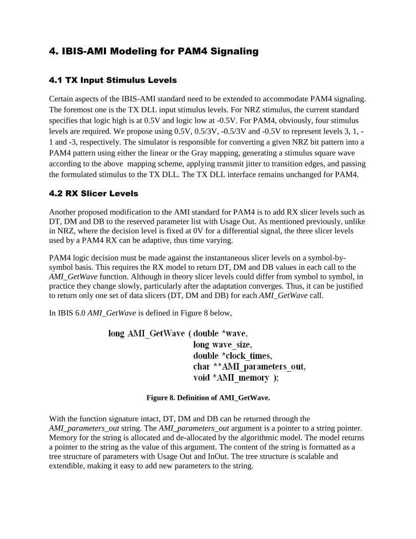
In IBIS 6.0 AMI_GetWave is defined in Figure 8 below,
Figure 8. Definition of AMI_GetWave.
With the function signature intact, DT, DM and DB can be returned through the
AMI_parameters_out string. The AMI_parameters_out argument is a pointer to a string pointer.
Memory for the string is allocated and de-allocated by the algorithmic model. The model returns
a pointer to the string as the value of this argument. The content of the string is formatted as a
tree structure of parameters with Usage Out and InOut. The tree structure is scalable and
extendible, making it easy to add new parameters to the string.
In each AMI_GetWave, the RX model will write name-value pairs of DT, DM and DB into the
AMI_parameters_out string and pass it back to the simulator, which will parse the string to
extract slicer levels. The values are used to decide PAM4 logic on symbols processed in this
AMI_GetWave call for SER or BER calculations.
It should be pointed out that in ADC-based receiver architecture the signal is sampled only once
per symbol and that the analog waveform does not exist in the physical device. However, for
AMI modeling the RX model can generate a hypothetically analog waveform by over-sampling
the signal.
4.3 Summary of Proposed Modification
In this section the following minimum modifications are proposed in order for the current AMI
model to handle PAM4 signal simulations:
It is proposed that {0.5V, 0.5/3V, -0.5/3V, -0.5V} are used to represent the 4 levels in PAM4,
{3, 1, -1 and -3}.
The simulator is responsible for converting a given NRZ bit pattern into a PAM4
pattern using a given mapping scheme.
The TX DLL interface remains unchanged for PAM4, thus no extra work the AMI
model developer.
It is proposed to add RX slicer levels to the reserved parameter list in AMI_GetWave with
Usage Out.
With the function signature intact, slicer levels can be returned through the
AMI_parameters_out string.
The simulator is responsible for all the post-processing work, such as generating eye
diagrams, calculating bathtub curves, and predicting system SER or BER.
It is proposed (details are in the next section) that a merged NRZ-equivalent eye can be
formulated through post processing in a simulator.
5. PAM4 Signal Measurement
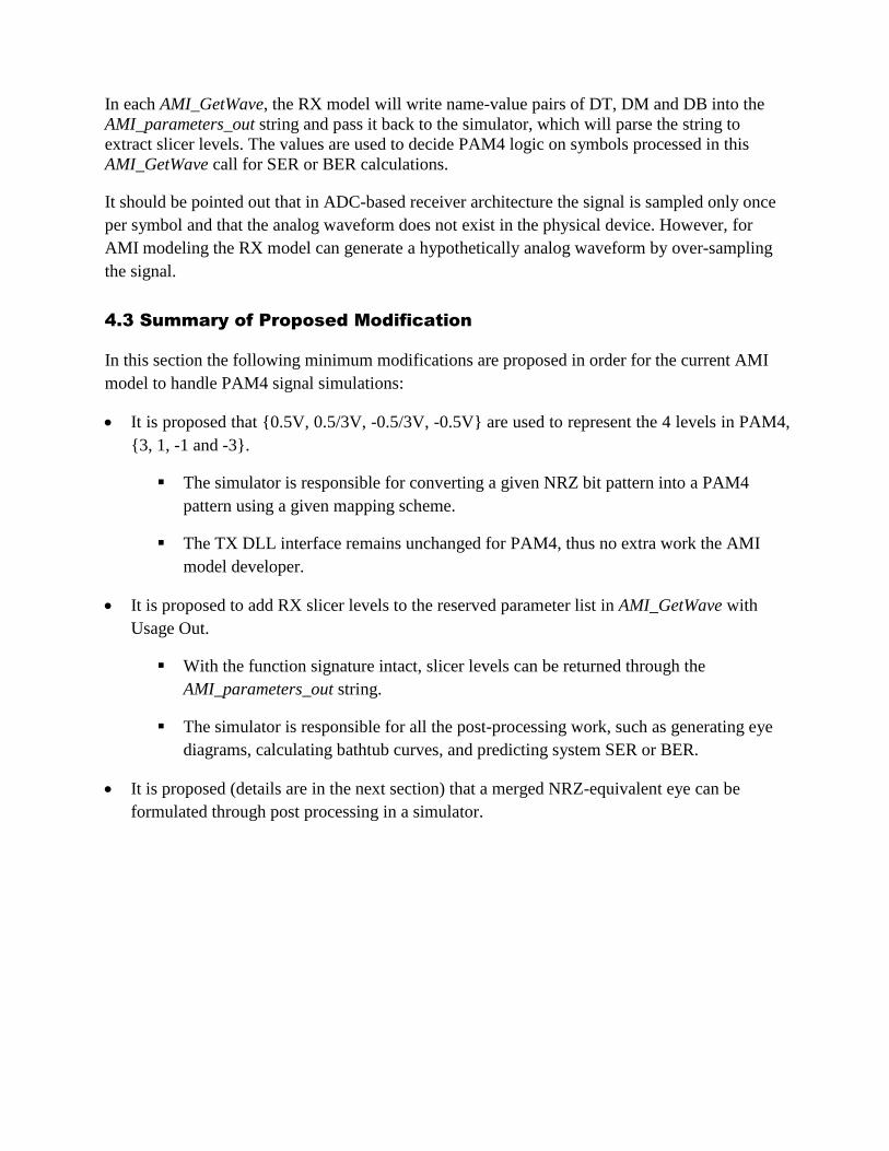
5.1 Eye Diagram
The conventional eye diagram can be constructed for PAM4; there are three vertically stacked
eyes in the diagram, corresponding to three decision levels. The eye diagram generation process
for PAM4 is identical to that for NRZ. An example of NRZ and PAM4 eyes is given in Figure 9.
Figure 9. Eye diagrams for NRZ and PAM4.
5.2 Bathtub Curve
For NRZ signal, timing and voltage bathtub curves are used to measure link performance. For
PAM4 signal, one set of bathtub curves can be plotted at each slicer level, giving three sets
bathtubs in total.
For RX, to track slicer level fluctuations, difference between the RX output signal and the
instantaneous level is used when constructing the RX bathtubs. For DT bathtubs, the logic high
branch consists of 𝑣3(𝑡) − 𝐷𝑇(𝑡) traces, where 𝑣3(𝑡) is the waveform of expected level 3
symbols and 𝐷𝑇(𝑡) the waveform of DT. The logic low branch contains 𝑣1(𝑡) − 𝐷𝑇(𝑡),
𝑣−1(𝑡) − 𝐷𝑇(𝑡) and 𝑣−3(𝑡) − 𝐷𝑇(𝑡) traces, where 𝑣1(𝑡), 𝑣−1(𝑡) and 𝑣−3(𝑡) are waveforms of
symbols with expected levels at 1, -1 and -3, respectively. For DM bathtubs, the logic high
branch is formed with 𝑣3(𝑡) − 𝐷𝑀(𝑡) and 𝑣1(𝑡) − 𝐷𝑀(𝑡) traces, and the logic low branch
𝑣−1(𝑡) − 𝐷𝑀(𝑡) and 𝑣−3(𝑡) − 𝐷𝑀(𝑡) traces, where 𝐷𝑀(𝑡) is the waveform of DM. For DB
bathtubs, the logic high branch is composed of 𝑣3(𝑡) − 𝐷𝐵(𝑡), 𝑣1(𝑡) − 𝐷𝐵(𝑡) and 𝑣−1(𝑡) −𝐷𝐵(𝑡) traces, and the logic low branch 𝑣−3(𝑡) − 𝐷𝐵(𝑡) traces, where 𝐷𝐵(𝑡) is the waveform of
DB. The procedure is shown in Table 1. Note that since the signal is adjusted with respect to
slicer levels in BER calculations, if levels vary with time, some discrepancy between bathtubs
and the conventional eye is expected.
Slicer level Logic high traces Logic low traces
DT 𝑣3(𝑡) − 𝐷𝑇(𝑡) 𝑣1(𝑡) − 𝐷𝑇(𝑡)
𝑣−1(𝑡) − 𝐷𝑇(𝑡)
𝑣−3(𝑡) − 𝐷𝑇(𝑡)
DM 𝑣3(𝑡) − 𝐷𝑀(𝑡)
𝑣1(𝑡) − 𝐷𝑀(𝑡)
𝑣−1(𝑡) − 𝐷𝑀(𝑡)
𝑣−3(𝑡) − 𝐷𝑀(𝑡)
DB 𝑣3(𝑡) − 𝐷𝐵(𝑡)
𝑣1(𝑡) − 𝐷𝐵(𝑡)
𝑣−1(𝑡) − 𝐷𝐵(𝑡)
𝑣−3(𝑡) − 𝐷𝐵(𝑡)
Table 1. Procedure of bathtub curve construction at each slicer level.
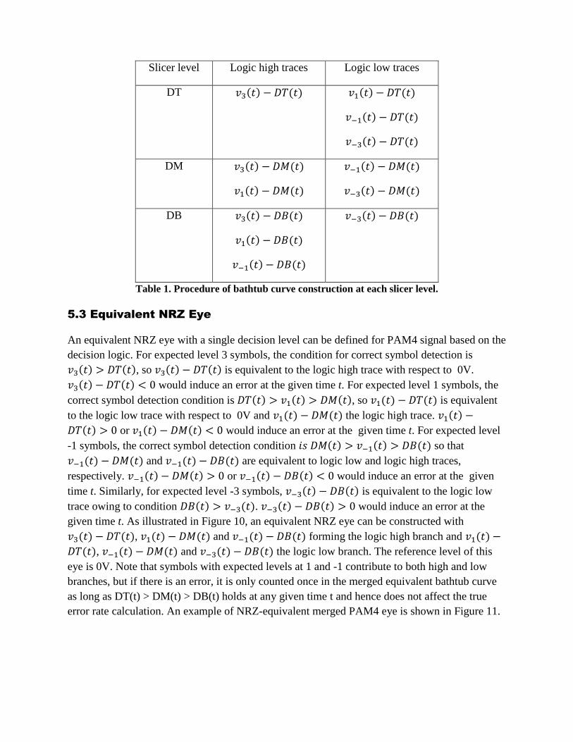
5.3 Equivalent NRZ Eye
An equivalent NRZ eye with a single decision level can be defined for PAM4 signal based on the
decision logic. For expected level 3 symbols, the condition for correct symbol detection is
𝑣3(𝑡) > 𝐷𝑇(𝑡), so 𝑣3(𝑡) − 𝐷𝑇(𝑡) is equivalent to the logic high trace with respect to 0V.
𝑣3(𝑡) − 𝐷𝑇(𝑡) < 0 would induce an error at the given time t. For expected level 1 symbols, the
correct symbol detection condition is 𝐷𝑇(𝑡) > 𝑣1(𝑡) > 𝐷𝑀(𝑡), so 𝑣1(𝑡) − 𝐷𝑇(𝑡) is equivalent
to the logic low trace with respect to 0V and 𝑣1(𝑡) − 𝐷𝑀(𝑡) the logic high trace. 𝑣1(𝑡) −
𝐷𝑇(𝑡) > 0 or 𝑣1(𝑡) − 𝐷𝑀(𝑡) < 0 would induce an error at the given time t. For expected level
-1 symbols, the correct symbol detection condition 𝑖𝑠 𝐷𝑀(𝑡) > 𝑣−1(𝑡) > 𝐷𝐵(𝑡) so that
𝑣−1(𝑡) − 𝐷𝑀(𝑡) and 𝑣−1(𝑡) − 𝐷𝐵(𝑡) are equivalent to logic low and logic high traces,
respectively. 𝑣−1(𝑡) − 𝐷𝑀(𝑡) > 0 or 𝑣−1(𝑡) − 𝐷𝐵(𝑡) < 0 would induce an error at the given
time t. Similarly, for expected level -3 symbols, 𝑣−3(𝑡) − 𝐷𝐵(𝑡) is equivalent to the logic low
trace owing to condition 𝐷𝐵(𝑡) > 𝑣−3(𝑡). 𝑣−3(𝑡) − 𝐷𝐵(𝑡) > 0 would induce an error at the
given time t. As illustrated in Figure 10, an equivalent NRZ eye can be constructed with
𝑣3(𝑡) − 𝐷𝑇(𝑡), 𝑣1(𝑡) − 𝐷𝑀(𝑡) and 𝑣−1(𝑡) − 𝐷𝐵(𝑡) forming the logic high branch and 𝑣1(𝑡) −
𝐷𝑇(𝑡), 𝑣−1(𝑡) − 𝐷𝑀(𝑡) and 𝑣−3(𝑡) − 𝐷𝐵(𝑡) the logic low branch. The reference level of this
eye is 0V. Note that symbols with expected levels at 1 and -1 contribute to both high and low
branches, but if there is an error, it is only counted once in the merged equivalent bathtub curve
as long as DT(t) > DM(t) > DB(t) holds at any given time t and hence does not affect the true
error rate calculation. An example of NRZ-equivalent merged PAM4 eye is shown in Figure 11.
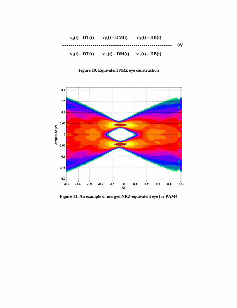
Figure 10. Equivalent NRZ eye construction
Figure 11. An example of merged NRZ-equivalent eye for PAM4
0V
v3(t) – DT(t) v1(t) – DM(t) v-1(t) – DB(t)
v1(t) – DT(t) v-1(t) – DM(t) v-3(t) – DB(t)
6. Example of Using AMI Model for PAM4 Simulations
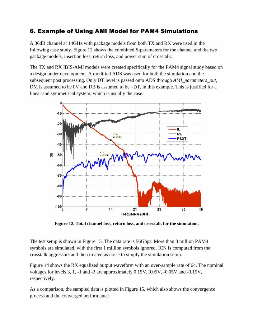
A 36dB channel at 14GHz with package models from both TX and RX were used in the
following case study. Figure 12 shows the combined S-parameters for the channel and the two
package models, insertion loss, return loss, and power sum of crosstalk.
The TX and RX IBIS-AMI models were created specifically for the PAM4 signal study based on
a design under development. A modified ADS was used for both the simulation and the
subsequent post processing. Only DT level is passed onto ADS through AMI_parameters_out,
DM is assumed to be 0V and DB is assumed to be –DT, in this example. This is justified for a
linear and symmetrical system, which is usually the case.
Figure 12. Total channel loss, return loss, and crosstalk for the simulation.
The test setup is shown in Figure 13. The data rate is 56Gbps. More than 3 million PAM4
symbols are simulated, with the first 1 million symbols ignored. ICN is computed from the
crosstalk aggressors and then treated as noise to simply the simulation setup.
Figure 14 shows the RX equalized output waveform with an over-sample rate of 64. The nominal
voltages for levels 3, 1, -1 and -3 are approximately 0.15V, 0.05V, -0.05V and -0.15V,
respectively.
As a comparison, the sampled data is plotted in Figure 15, which also shows the convergence
process and the converged performance.
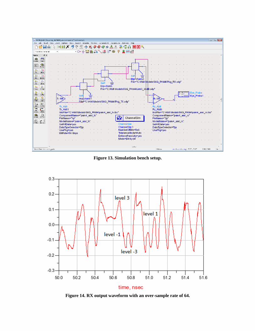
Figure 13. Simulation bench setup.
Figure 14. RX output waveform with an over-sample rate of 64.
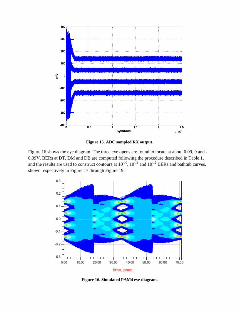
Figure 15. ADC sampled RX output.
Figure 16 shows the eye diagram. The three eye opens are found to locate at about 0.09, 0 and -
0.09V. BERs at DT, DM and DB are computed following the procedure described in Table 1,
and the results are used to construct contours at 10-10
, 10-11
and 10-12
BERs and bathtub curves,
shown respectively in Figure 17 through Figure 19.
Figure 16. Simulated PAM4 eye diagram.
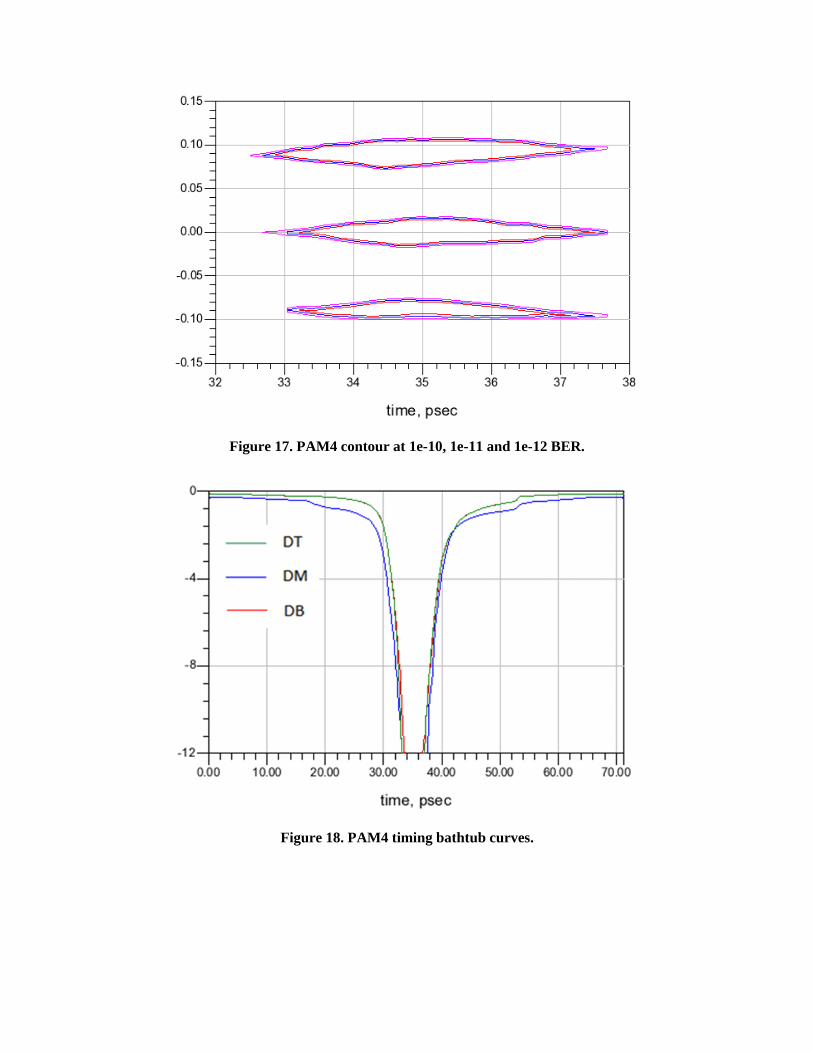
Figure 17. PAM4 contour at 1e-10, 1e-11 and 1e-12 BER.
Figure 18. PAM4 timing bathtub curves.
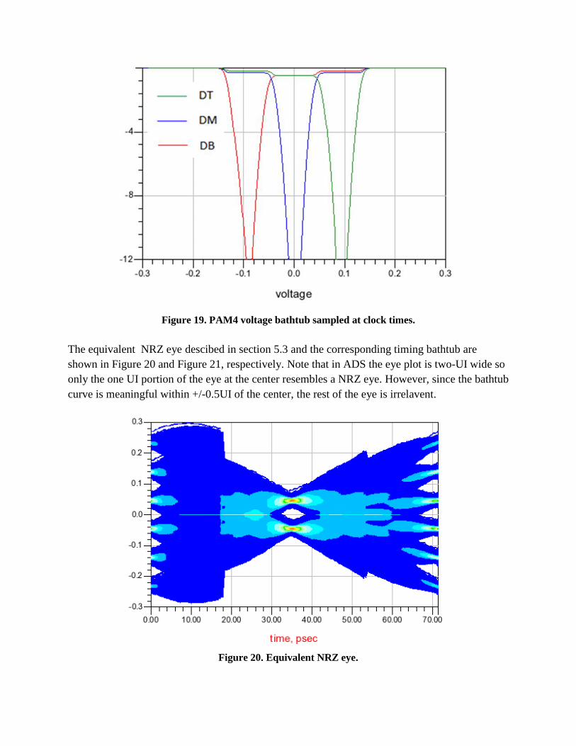
Figure 19. PAM4 voltage bathtub sampled at clock times.
The equivalent NRZ eye descibed in section 5.3 and the corresponding timing bathtub are
shown in Figure 20 and Figure 21, respectively. Note that in ADS the eye plot is two-UI wide so
only the one UI portion of the eye at the center resembles a NRZ eye. However, since the bathtub
curve is meaningful within +/-0.5UI of the center, the rest of the eye is irrelavent.
Figure 20. Equivalent NRZ eye.
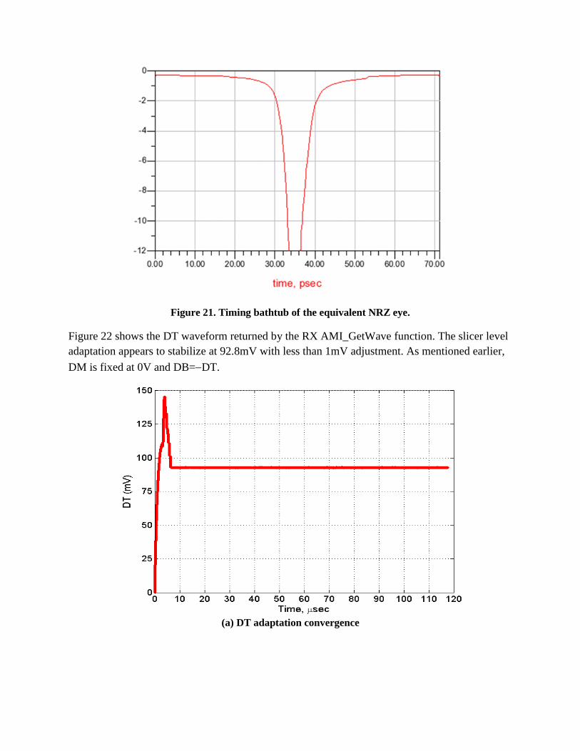
Figure 21. Timing bathtub of the equivalent NRZ eye.
Figure 22 shows the DT waveform returned by the RX AMI_GetWave function. The slicer level
adaptation appears to stabilize at 92.8mV with less than 1mV adjustment. As mentioned earlier,
DM is fixed at 0V and DB=DT.
(a) DT adaptation convergence
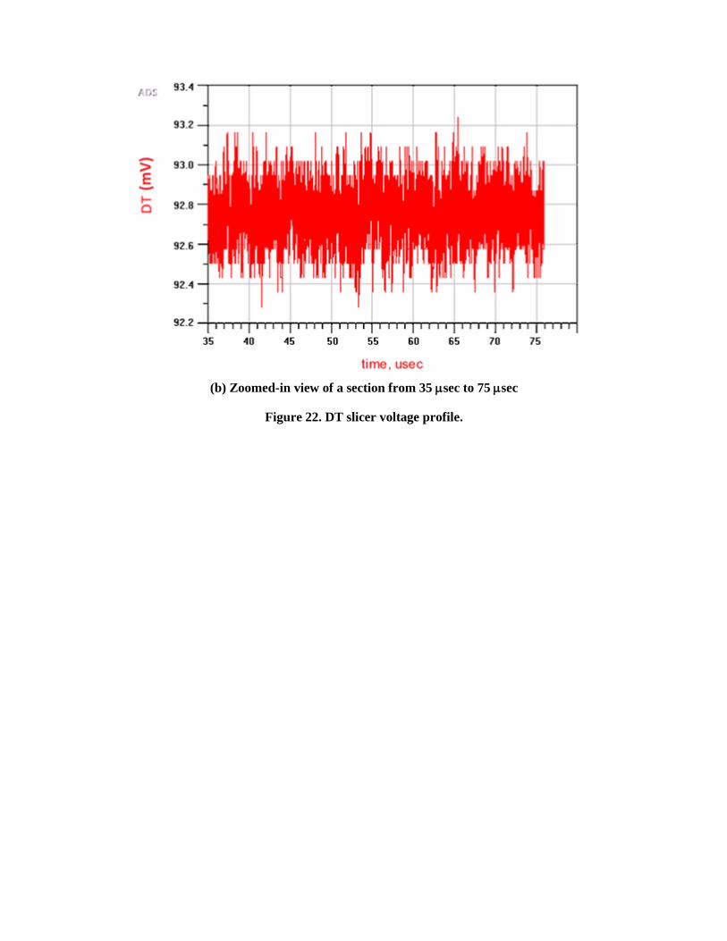
(b) Zoomed-in view of a section from 35 sec to 75 sec
Figure 22. DT slicer voltage profile.
7. Conclusions and Future Work
In this paper, we proposed a method to extend IBIS AMI standard for PAM4 signaling.
Specifically, TX needs to send 4 different levels while RX needs to pass on adapted slicer levels
to the EDA tool using AMI_parameters_out through AMI_GetWave function calls. We verified
this proposal through simulations in the modified ADS. Three vertical bathtub curves, three
horizontal bathtub curves or three BER contours are needed to fully evaluate the performance
margin of the link system using PAM4. We also proposed a procedure to construct the equivalent
NRZ eye with a single reference level at 0V.
We have decided that only one reference level is needed for PAM4 as all the slicing levels are
symmetrical and linearly related. However, if multiple reference levels are needed to account for
strong nonlinearity or asymmetrical behavior of the real circuits, we need to pass on three slicing
levels to the EDA from the model output for post processing. In addition, we only used one
reference level for the entire AMI_GetWave block. This is justified as a stable and settled
reference adaptation loop is not expected to deviate much from bit to bit. If an unstable reference
adaptation loop is expected or if the detailed reference adaptation settling behavior is to be
observed, the AMI model would need to pass on the entire adaptation sequence to the EDA tool,
which cannot be supported using the existing IBIS-AMI standard.
Some IBIS parameters such as ramp rate may need to be separately defined between each signal
level to accurately describe the analog behavior of the circuits. This is not within the scope of
this paper and can be further explored in the future.
To support both PAM4 and NRZ signaling scheme, an EDA tool should be able to switch
between the two modes and preferably can automatically pass on the information to the IBIS-
AMI model. This remains to be further investigated and standardized.
To calculate true BER, received signal is often correlated with the transmitted signal. If TX
model contains a coding scheme , for example, Gray coding, for BER improvement while the
RX model (from a different vendor) does not have, then an EDA tool is desired to have an option
added to do the decoding work. All this remains to be further discussed.
References
[1] IEEE P802.3bj™/D3.2, “Draft Standard for Ethernet Amendment 2: Physical Layer
Specifications and Management Parameters for 100 Gb/s Operation Over Backplanes and
Copper Cables
[2] J. L. Zerbe et aI., "Equalization and clock recovery for a 2.5-1 O-Gb/s 2-PAM/4-PAM
backplane transceiver cell," IEEE 1. Solid-State Circuits, vol. 38, no. 12, pp. 2121-2130, Dec.
2003.
[3] J. T. Stonick, G. Y. Wei, 1. L. Sonntag, and D. K. Weinlader, "Anadaptive PAM-4 5-Gb/s
backplane transceiver in 0.25 um CMOS, IEEE 1. Solid-State Circuits, vol. 38, no. 3, pp.
436-443, Mar. 2003.
[4] Kian Haur (Alfred) Chong, Venkatesh Avula, Liu Liang, Srikanth Pam, Makram Mansour,
and Fangyi Rao, “IBIS AMI Modeling of Retimer and Performance Analysis of Retimer
based Active Serial Links”, DesignCon 2014.
[5] “NOTES ON ALGORITHMIC MODELING INTERFACE AND PROGRAMMING
GUIDE”, https://www.google.com/webhp?sourceid=chrome-
instant&rlz=1C1KMZB_enUS596US596&ion=1&espv=2&ie=UTF-
8#q=IBIS_Section_10_rc01.docx
[6] Sam Palermo, “Lecture 9: Modulation Schemes ECEN689: Special Topics in High-Speed
Links Circuits and Systems”, Spring 2010.
[7] http://publications.lib.chalmers.se/records/fulltext/170236/local_170236.pdf


![DesignCon 2020...1 DesignCon 2020 DfA (Design for AMI) – A New Integrated Workflow for Modeling 56G PAM4 SerDes Systems Jonggab Kil, Intel [jonggab.kil@intel.com] Vijay Kasturi,](https://img.pdfslide.net/doc/110x75/5f84974871df87322928d571/designcon-2020-1-designcon-2020-dfa-design-for-ami-a-a-new-integrated-workflow.jpg)