Embed Size (px)
Citation preview
DETERMINATION AND CHARACTERIZATION OF LEAD FREE SOLDER ALLOYS
A Thesis Submitted in Partial Fulfillment of the Requirements for the
Degree of
Master of Technology
In
Metallurgical and Materials Engineering
SUBMITTED BY
PRERNA MISHRA
DEPARTMENT OF METALLURGICAL AND MATERIALS ENGINEERING
NATIONAL INSTITUTE OF TECHNOLOGY, ROURKELA
2014
DETERMINATION AND CHARACTERIZATION
OF LEAD FREE SOLDER ALLOYS
A thesis
Submitted by
Prerna Mishra
(212MM1451)
In partial fulfillment of the requirements
for the award of the degree of
Master of Technology
In
Metallurgical and Materials Engineering
(Metallurgical and Materials Engineering)
Under The Guidance of
Dr. S.N Alam
Department of Metallurgical and Materials Engineering
National Institute of Technology Rourkela
Orissa -769008, India
May 2014
NATIONAL INSTITUTE OF TECHNOLOGY ROURKELA, ORISSA -769008, INDIA
This is to certify that the thesis entitled, “DETERMINATION AND CHARACTERIZATION
OF LEAD FREE SOLDER ALLOYS” submitted by Prerna Mishra in partial fulfillment of
the requirement for the award of Master of Technology degree in Metallurgical and Materials
Engineering with specialization in Metallurgical and Materials Engineering at the National
Institute of Technology Rourkela is an authentic work carried out by her under our supervision
and guidance. To the best of our knowledge, the matter embodied in the thesis has not been
submitted to any other University/Institute for the award of any degree or diploma.
Research Guide
Place: Rourkela Dr. S.N ALAM
Assistant Professor
National Institute Of Technology
Date:

i
ACKNOWLEDGEMENTS
First and foremost, praise and thanks goes to my God for the blessing that has bestowed upon me
in all my endeavors.
I am deeply indebted to Dr. S.N Alam, Assistant Professor of Metallurgical and Materials
Engineering Division, my advisor and guide, for the motivation, guidance, tutelage and patience
throughout the research work. I appreciate his broad range of expertise and attention to detail, as
well as the constant encouragement he has given me over the years. There is no need to mention
that a big part of this thesis is the result of joint work with him, without which the completion of
the work would have been impossible.
I am grateful to Prof. B.C Ray, Head of the Department of Metallurgical and Materials
Engineering for providing me necessary facility for my work. I express my sincere thanks to Prof
A. K Mondal, the M.Tech Project coordinators of Metallurgical & Materials Engineering
department.
Special thanks to my family members always encouraging me for higher studies, all department
members specially Mr. Rajesh, Mr.U.K Sahoo, Mr.Hembram, Mr.A.Pal and Mr.K.Tanty and all
my friends of department of Metallurgical and Materials Engineering for being so supportive and
helpful in every possible way.
I am grateful for friendly atmosphere of the Metallurgical and Materials Engineering Division
and all kind and helpful professors that I have met during my course.
Prerna Mishra
ii
ABSTRACT
In recent years the development of lead free solders has emerged as one of the key issues in the
electronic industries .So far eutectic or near eutectic Sn – Pb alloys have been widely used due to
their low melting temperature and good wettability. Sn – Zn solder alloys have been considered
as one of the most attractive lead free system that can replace toxic Sn – Pb solder without
increasing the soldering temperature. However there are some drawbacks in Sn – Zn lead free
system such as poor oxidation resistance, wettability and embrittlement behavior. In order to
overcome these drawbacks and to further enhance the properties of Sn- Zn solder a small
amount of alloying elements like Bi (Bismuth), Ag (Silver), Al (Aluminium), Cu (Copper), In
(Indium), Chromium (Cr), Antimony (Sb), Nickel (Ni), Ge (Germanium) were added.
This work aims to investigate the effect of Bi (Bismuth) addition on the microstructure, thermal
and mechanical properties of Sn – Zn lead free system. The microstructure of all the solder
alloys was investigated using a Scanning electron microscope (SEM). The composition of the
solder alloys was determined using Energy dispersive X- ray spectroscopy (EDX). Differential
scanning calorimetry (DSC) was done to find out the melting temperature of the alloys. Phase
analysis for the alloys was done using X- ray diffraction. Tensile test was performed to find out
the mechanical properties of the alloys.
iii
TABLE OF CONTENTS
Title Page No
ACKNOWLEDGEMENT i
ABSTRACT ii
TABLES OF CONTENT iii
LIST OF FIGURE vi
LIST OF TABLE viii
ABBREVIATIONS ix
CHAPTER 1 INTRODUCTION
1.1INTRODUCTION 1
1.2OBJECTIVE OF THE WORK 4
CHAPTER 2 LITERATURE REVIEW
2.1 ELECTRONIC PACKAGING 5
2.2. THE APPLICATIONS 6
2.3 SOLDERING AND ITS REVIEW 6
2.4 SOLDERING MATERIALS 7
2.5 SOLDERING METHODS 7
2.5.1 REFLOW SOLDERING 7
2.5.2 WAVE SOLDERING 8
2.6 GENERAL CRITERIA TO SELECT A SOLDER ALLOY 8
2.7 USEFUL PROPERTIES OF Sn-Pb 9
2.8 ROLE OF Pb IN Sn-Pb SOLDERS 9
2.9 ROLE OF Sn 10
2.9.1 CRYSTALLOGRAPHIC PROPERTIES 10
2.9.2 MECHANICAL PROPERTIES 10
2.9.3 CHEMICAL PROPERTIES 11
iv
2.10 SOURCE OF EXPOSURE 11
2.11 Pb BASED MATERIALS - THE ISSUES 12
2.11.1 LEAD POISIONING 12
2.11.2 ADVERSE EFFECTS OF Pb ON HUMAN LIFE 12
2.11.3 ADVERSE EFFECTS OF Pb IN ENVIRONMENT AND OTHER SPECIES 13
2.12 Pb BASED MATERIALS – THE LEGISLATIONS 14
2.13 Pb FREE MATERIALS – THE PROBLEMS 15
2.14 Pb FREE INTERCONNECT MATERIALS FOR ELECTRONIC PACKAGE 16
2.15 Pb FREE MARETIALS – THE REAL DEFINITIONS 16
2.16 ALLOYS AS GREEN SOLDERS 17
2.17 IMPORTANT LEAD FREE SOLDERS 18
2.18 SOLDERABILITY AND WETTABILITY 22
2.19 FORMATION OF INTERMETALLICS 22
CHAPTER 3 EXPERIMENTAL SETUP AND METHODOLOGY
3.1. MATERIALS 24
3.2 FLOW-CHART OF THE EXPERIMENTAL PROCEDURE 25
3.3 METALLOGRAPHY 26
3.4 EXPERIMENTAL INSTRUMENTS 26
3.4.1 TUBULAR FURNACE 26
3.4.2 SCANNING ELECTRON MICROSCOPE 27
3.4.3 ENERGY DISPERSIVE X- RAY SPECTROSCOPY 28
3.4.4 DIFFERENTIAL SCANNING CALORIMETRY 29
3.4.5 X-RAY DIFFRACTION 30
3.4.6 UNIVERSAL TESTING MACHINE 30
CHAPTER 4 EXPERIMENTAL RESULTS
4.1. Sn-Zn EUTECTIC PHASE DIAGRAM 31
4.2 Sn-8Zn 31
4.2.1 MICROSTRUCTURAL AND ELEMENTAL ANALYSIS OF Sn-8Zn 31
4.2.2 THERMAL ANALYSIS OF Sn-8Zn 34
4.2.3 WETTING ANALYSIS OF Sn-8Zn 34
4.3 Sn-8Zn-3Bi 35
v
4.3.1 MICROSTRUCTURAL AND ELEMENTAL ANALYSIS OF Sn-8Zn-3Bi 35
4.3.2 PHASE DIAGRAM OF Sn-Bi and Zn-Bi 36
4.3.3 THERMAL ANALYSIS OF Sn-8Zn-3Bi 37
4.3.4 WETTING ANALYSIS OF Sn-8Zn-3Bi 38
4.4 Sn-8Zn-6Bi 38
4.4.1 MICROSTRUCTURAL AND ELEMENTAL ANALYSIS OF Sn-8Zn-6Bi 38
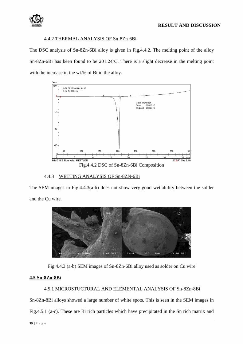
4.4.2 THERMAL ANALYSIS OF Sn-8Zn-6Bi 40
4.4.3 WETTING ANALYSIS OF Sn-8Zn-6Bi 40
4.5 Sn-8Zn-8Bi 40
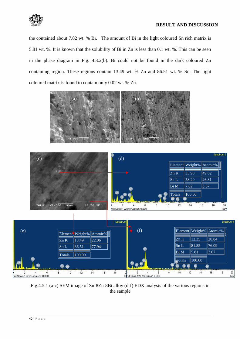
4.5.1 MICROSTRUCTURAL AND ELEMENTAL ANALYSIS OF Sn-8Zn-8Bi 40
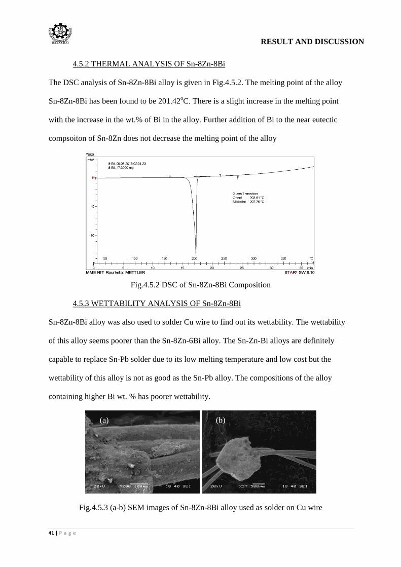
4.5.2 THERMAL ANALYSIS OF Sn-8Zn-8Bi 42
4.5.3 WETTING ANALYSIS OF Sn-8Zn-8Bi 42
4.6 Sn-8Zn-10Bi 43
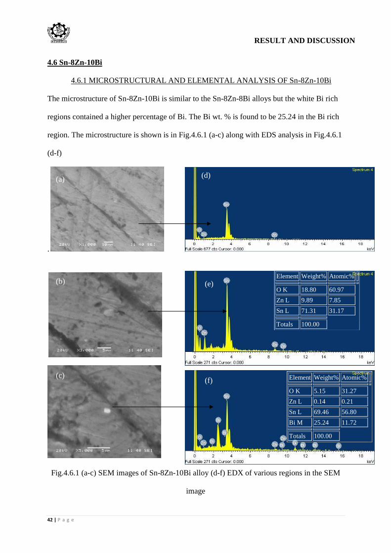
4.6.1 MICROSTRUCTURAL AND ELEMENTAL ANALYSIS of Sn-8Zn-10Bi 43
4.6.2 THERMAL ANALYSIS OF Sn-8Zn-10Bi 44
4.7 X – RAY DIFFRACTION ANALYSIS 44
4.8 FORMATION OF INTERMETALLICS 45
4.9 VARIATION OF MELTING POINT WITH ADDITION OF Bi 46
4.10 VARIATION OF MECHANICAL PROPERTIES 47
4.11 FRACTOGRAPHY 48
4.12 Sn-Zn-Ag 49
4.12.1 MICROSTRUCTURAL AND ELEMENTAL
ANALYSIS OF Sn-Zn-Ag SOLDERS 50
4.12.2 THERMAL ANALYSIS OF Sn-Zn-Ag SOLDERS 51
4.12.3 X-RAY DIFFRACTION ANALYSIS OF Sn-Zn-Ag SOLDERS 53
4.12.4 VARIATION OF MELTING TEMPERATURE OF Sn-Zn-Ag SOLDERS 54
CHAPTER 5
5.1. CONCLUSION 55
5.2. SCOPE FOR FUTURE WORK 56
REFERENCES 57
vi
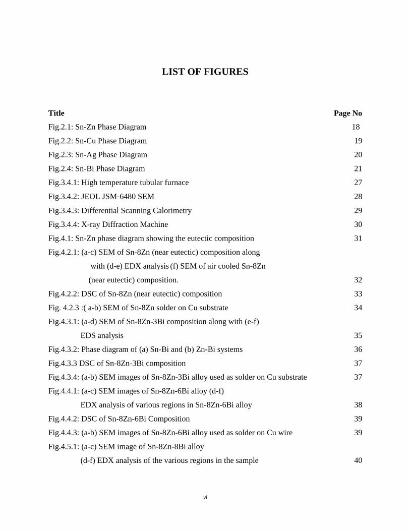
LIST OF FIGURES
Title Page No
Fig.2.1: Sn-Zn Phase Diagram 18
Fig.2.2: Sn-Cu Phase Diagram 19
Fig.2.3: Sn-Ag Phase Diagram 20
Fig.2.4: Sn-Bi Phase Diagram 21
Fig.3.4.1: High temperature tubular furnace 27
Fig.3.4.2: JEOL JSM‐6480 SEM 28
Fig.3.4.3: Differential Scanning Calorimetry 29
Fig.3.4.4: X-ray Diffraction Machine 30
Fig.4.1: Sn-Zn phase diagram showing the eutectic composition 31
Fig.4.2.1: (a-c) SEM of Sn-8Zn (near eutectic) composition along
with (d-e) EDX analysis (f) SEM of air cooled Sn-8Zn
(near eutectic) composition. 32
Fig.4.2.2: DSC of Sn-8Zn (near eutectic) composition 33
Fig. 4.2.3 :( a-b) SEM of Sn-8Zn solder on Cu substrate 34
Fig.4.3.1: (a-d) SEM of Sn-8Zn-3Bi composition along with (e-f)
EDS analysis 35
Fig.4.3.2: Phase diagram of (a) Sn-Bi and (b) Zn-Bi systems 36
Fig.4.3.3 DSC of Sn-8Zn-3Bi composition 37
Fig.4.3.4: (a-b) SEM images of Sn-8Zn-3Bi alloy used as solder on Cu substrate 37
Fig.4.4.1: (a-c) SEM images of Sn-8Zn-6Bi alloy (d-f)
EDX analysis of various regions in Sn-8Zn-6Bi alloy 38
Fig.4.4.2: DSC of Sn-8Zn-6Bi Composition 39
Fig.4.4.3: (a-b) SEM images of Sn-8Zn-6Bi alloy used as solder on Cu wire 39
Fig.4.5.1: (a-c) SEM image of Sn-8Zn-8Bi alloy
(d-f) EDX analysis of the various regions in the sample 40
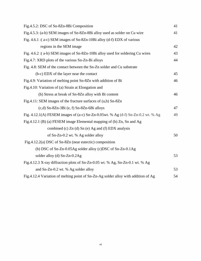
vii
Fig.4.5.2: DSC of Sn-8Zn-8Bi Composition 41
Fig.4.5.3: (a-b) SEM images of Sn-8Zn-8Bi alloy used as solder on Cu wire 41
Fig. 4.6.1 :( a-c) SEM images of Sn-8Zn-10Bi alloy (d-f) EDX of various
regions in the SEM image 42
Fig. 4.6.2 :( a-b) SEM images of Sn-8Zn-10Bi alloy used for soldering Cu wires 43
Fig.4.7: XRD plots of the various Sn-Zn-Bi alloys 44
Fig. 4.8: SEM of the contact between the Sn-Zn solder and Cu substrate
(b-c) EDX of the layer near the contact 45
Fig.4.9: Variation of melting point Sn-8Zn with addition of Bi 46
Fig.4.10: Variation of (a) Strain at Elongation and
(b) Stress at break of Sn-8Zn alloy with Bi content 46
Fig.4.11: SEM images of the fracture surfaces of (a,b) Sn-8Zn
(c,d) Sn-8Zn-3Bi (e, f) Sn-8Zn-6Bi alloys 47
Fig. 4.12.1(A) FESEM images of (a-c) Sn-Zn-0.05wt. % Ag (d-f) Sn-Zn-0.2 wt. % Ag 49
Fig.4.12.1 (B) (a) FESEM image Elemental mapping of (b) Zn, Sn and Ag
combined (c) Zn (d) Sn (e) Ag and (f) EDX analysis
of Sn-Zn-0.2 wt. % Ag solder alloy 50
Fig.4.12.2(a) DSC of Sn-8Zn (near eutectic) composition
(b) DSC of Sn-Zn-0.05Ag solder alloy (c)DSC of Sn-Zn-0.1Ag
solder alloy (d) Sn-Zn-0.2Ag 53
Fig.4.12.3 X-ray diffraction plots of Sn-Zn-0.05 wt. % Ag, Sn-Zn-0.1 wt. % Ag
and Sn-Zn-0.2 wt. % Ag solder alloy 53
Fig.4.12.4 Variation of melting point of Sn-Zn-Ag solder alloy with addition of Ag 54
viii
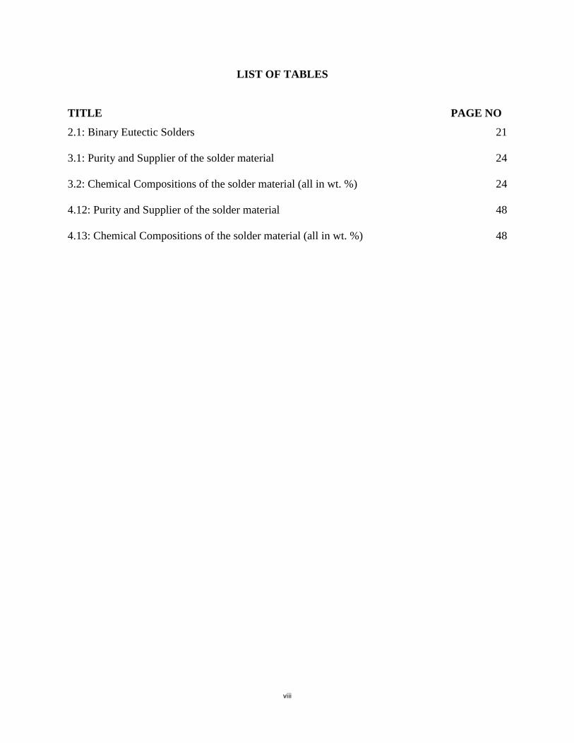
LIST OF TABLES
TITLE PAGE NO
2.1: Binary Eutectic Solders 21
3.1: Purity and Supplier of the solder material 24
3.2: Chemical Compositions of the solder material (all in wt. %) 24
4.12: Purity and Supplier of the solder material 48
4.13: Chemical Compositions of the solder material (all in wt. %) 48
ix
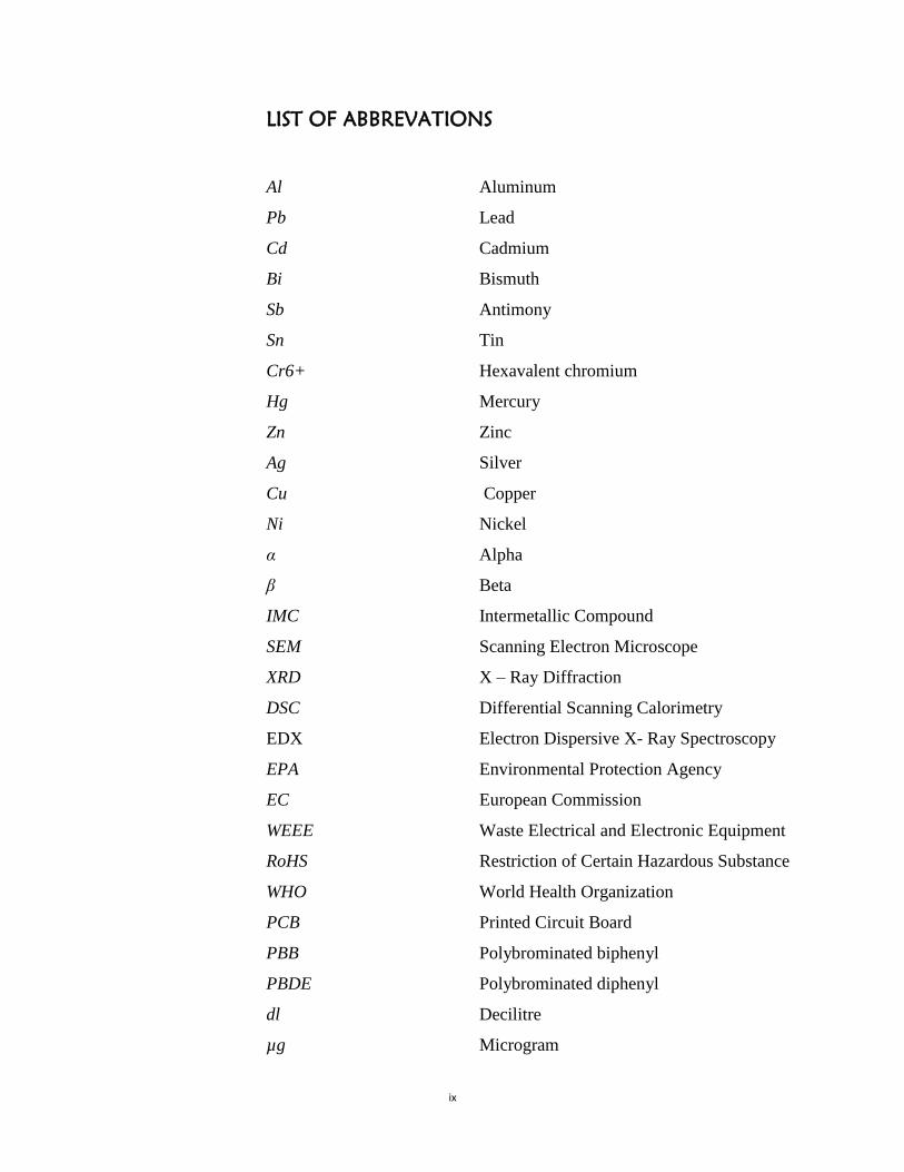
LIST OF ABBREVATIONS
Al Aluminum
Pb Lead
Cd Cadmium
Bi Bismuth
Sb Antimony
Sn Tin
Cr6+ Hexavalent chromium
Hg Mercury
Zn Zinc
Ag Silver
Cu Copper
Ni Nickel
α Alpha
β Beta
IMC Intermetallic Compound
SEM Scanning Electron Microscope
XRD X – Ray Diffraction
DSC Differential Scanning Calorimetry
EDX Electron Dispersive X- Ray Spectroscopy
EPA Environmental Protection Agency
EC European Commission
WEEE Waste Electrical and Electronic Equipment
RoHS Restriction of Certain Hazardous Substance
WHO World Health Organization
PCB Printed Circuit Board
PBB Polybrominated biphenyl
PBDE Polybrominated diphenyl
dl Decilitre
µg Microgram
x
mg Milligram
l Litre
wt.% Weight percentage
TV Television
CD Compact Disk
NC Numeric Control
LAN Local Area Network
ECG Electro Cardiogram
PbCO3 Lead Carbonate
ZnO Zinc Oxide
kN Kilo Newton

CHAPTER 1
INTRODUCTION
INTRODUCTION
1 | P a g e
1. INTRODUTION
Solder alloys have been widely used as the interconnecting material in electronic packaging and
assemblies because they provide both electrical interconnection as well as mechanical support.
Sn-Pb solders were first used about 2000 years ago for metal inter connections. Pb containing
solders especially the eutectic or near eutectic Sn-Pb alloys has long been the predominant
choice of the electronics industry due to its low melting temperature (around 183oC),better
wetting behavior and mechanical properties [1] [2] [3]. Despite of all these advantages the
toxicity of heavy metallic element Pb has led in recent decades to increasing efforts to restrict its
use. Following the banning of Pb in paints, fuels and plumbing application throughout the
majority of the world, otherwise it could be demonstrated to present a direct risk to human health
and environment [4].
Science and engineering of soldering has taken a major change in direction ever since the
legislation that mandates restriction of certain hazardous substances (RoHS) [5] and the waste
electrical and electronic equipment (WEEE) [6] had been introduced by many countries. The
first administrative region of the world to actively legislate against Pb use in electronics has been
the European Union, which has introduced RoHS and WEEE directives. These directives target
the electrical and electronic equipment and are designed respectively to outlaw many harmful
substances from use and make the producers of electrical and electronic goods responsible for
their safe disposal or recycling at the end of their lives.
As cited by Environmental Protection Agency (EPA) of US, Pb and Pb containing compounds is
one of the top 17 chemicals causing greatest threat to human life and environment.1st July 2006
has been officially designated by European Union as the date when the “Directive on the
Restriction of Hazardous substances in Electrical and Electronic equipment will require “the use
INTRODUCTION
2 | P a g e
of lead (Pb), mercury (Hg), cadmium (Cd), hexavalent chromium (Cr6+) and halogenated flame
retardants” be phased out. This led to the development of lead free solders which has emerged as
one of the key issues in electronic packaging and industries [7] [8] [9].
For developing a new solder one need to think of various properties such as melting temperature,
mechanical properties, microstructure, wettability, and pasty range, solder ability, reliability and
cost of solder joints [10] [11]. One major limiting factor in the selection of a Pb free alloy is that
the entire electronics manufacturing industry is accustomed to the low melting point of the
eutectic Sn- Pb alloy (183oC) and components are designed to withstand soldering temperature
associated with this. Any rise in the processing temperature of printed circuit boards (PCBs) will
have adverse effects on component reliability. This narrow window of melting points restricts
research to a handful of alternative alloys based on Sn with other elements added. Alongside the
temperature requirements, there are number of metallurgical and mechanical properties of Sn-Pb
which an alternative alloy has to rival in order for it to be a successful replacement.
Researchers have developed a large number of binary Pb free solder alloys such as Sn-Zn, Sn-
Cu, Sn-Ag, Sn-Bi, Sn-Sb and Sn-In. Among these binary systems Sn-Zn solder alloys possess
several fascinating features such as Sn-9Zn eutectic alloy has melting temperature (198oC) very
close to that of Sn-Pb eutectic alloy (183oC) and also offers better mechanical properties as
compared to conventional Sn-Pb solders. In addition to this it has low cost as well as low reflow
temperature of 222oC also nontoxic to human health and environment [12] [13] [14]. Sn-Zn
solders are quite capable in terms of mechanical integrity but have poor oxidation and corrosion
resistance [15] [16] [17] [18]. The wettability of Sn-Zn solder has been an important issue
because during soldering the highly active Zn atoms get oxidized forming voids at the interface.
Zinc oxide formed by the oxidation of Zn floats on the liquid surface and prevents the solder
INTRODUCTION
3 | P a g e
from wetting the substrate [19] [20]. Therefore the Sn-Zn eutectic solder is difficult to handle
due to its poor wettability, reliability, strength, easy oxidation and microvoid formation. In order
to overcome these drawbacks and to further enhance the properties of Sn-Zn lead free system
small amount of alloying elements such as Bi, Cu, In, Ag, Al, Ga, Sb, Cr, Ni, Ge were added to
develop ternary and even quaternary Pb free systems as suggested by many researchers [21] [22]
[23] [24].
It has been found that the addition of Bi to the eutectic composition of Sn-Zn lead free system
has improved various soldering properties. Addition of Bi decreases the melting point of the
system and improves the wettability of Sn-Zn solder on Cu substrate. The wetting area increases
by 2 -10 wt% approximately on addition of Bi content. On addition of Bi the surface tension of
the solder has been decreased which has enhanced its wettability. Similarly the mechanical
properties of the Sn-Zn solder have been improved on Bi addition but up to a certain extent [25]
[26].
INTRODUCTION
4 | P a g e
1.1OBJECTIVE
Objective of this work is to prepare the different types of lead free solder alloys and to
investigate the effects of Bi addition on the microstructure, melting behavior, mechanical
properties, wettability and X- ray diffraction pattern of solidified Sn – Zn solder alloy. Objective
of this work are –
1. Determination of microstructure and compositional analysis of lead free solder alloys by
Scanning electron microscope (SEM) and Energy Dispersive X – ray spectroscopy (EDS
or EDX).
2. Phase Analysis by X – ray diffraction technique (XRD).
3. Determination of Melting point of the alloys by Differential Scanning Calorimetry
(DSC).
4. Determination of Ultimate Tensile Strength by Universal Testing Machine (UTM).

CHAPTER 2
LITERATURE
REVIEW
LITERATURE REVIEW
5 | P a g e
2.1 ELECTRONIC PACKAGING
Electronic packaging refers to the method of enclosing, protecting and providing physical
structure to electronic devices, components and assemblies. In recent years, electronic devices
require more resistors, transistors or diodes on a single semiconductor chip. All these discrete
circuit components are embedded in or on the chip and are connected to the printed circuit board
(PCB). Through various technologies establishment of interconnections for all these tiny
components can be achieved. Large amount of heat is generated when the device is in operation
and this heat has to be removed so that the device can perform its functions properly.
Semiconductor chips are fragile and require ‘armour’ coating to protect them from chemical,
mechanical and environmental damage. Hence, the concept of “electronic packaging” has been
introduced to describe manufacturing process or the hardware that provide the electrical
connections, the removal of excessive heat and the protection from environmental damage [27]
[28].
2.2 THE APPLICATIONS
The electronic packaging assemblies are used in following areas: [29]
Computers and Business Equipment: Calculators, printers, desktop computers,
photocopiers, workstations, personal digital assistants, high performance computers etc.
Communications: Cellular phones, handsets, line cards, LAN cards and switches, modems,
fax machines, routers, pagers, main switches etc.
Automotive Electronics: Engine control and management systems, transmission
controllers, braking controllers, traction controllers, suspension, wipers, lighting, air
conditioning and heating, safety, electronic dashboard, convenience and entertainment
systems etc.
LITERATURE REVIEW
6 | P a g e
Consumer Electronics: VCR, CD players, watches, compact audio systems, portable audio
players, smart cards, microwave, ovens, TV sets, game systems and cartridges etc.
Industrial and medical systems: Test and measuring devices and instruments, process
control systems, motor controls, calibrators, uninterruptible power systems, NC controls,
robotics, ECGs, implants medical imaging systems etc.
Military Electronics: Mobile Communications, missiles, avionics radar, satellite links land
– based radar and communication systems.
2.3 SOLDERING AND ITS REVIEW
Soldering is a process in which two or more metals are joined together by melting and flowing a
filler metal (solder) into the joints with a melting temperature well below those of the substrates
and typically less than 450o
C.The term “solder” refers to a group of metal alloys which melt at
relatively low temperatures and whose purpose is to form a joint between two others, possibly
dissimilar materials.The distinction between soldering and brazing is only the temperature at
which the joining operation takes place; around 450oC in the case of soldering.Both these
techniques involve a filler metal which in the molten state adheres to the two substrates by
capillary action to be joined, then freezes to form a permanent joint, as opposed to welding
where the substrates themselves are melted to fuse together. The most common alloy system in
soldering is that of Sn and Pb. Their relative proportions in a binary alloy can be varied to give
melting points up to that of pure Pb (327.5oC) but the most important ratio is 63 Sn/37Pb (wt.%),
which is the eutectic point.This eutectic mixture melts sharply at 183oC and is used universally to
join wires and components in electronic circuits and assemblies, manually or by automated
processes [30].
LITERATURE REVIEW
7 | P a g e
2.4 SOLDERING MATERIALS
There are a range of solder alloys that are used for soldering interconnections. These solders are
basically alloys of tin (Sn) and one or more of the following elements: Lead(Pb), Silver(Ag),
Bismuth(Bi), Indium(In), Antimony(Sb), Cadmium(Cd), Zinc(Zn), Copper(Cu), Nickel(Ni) etc.
If a solder alloys solidus and liquidus temperatures are identical it is called eutectic solder alloy,
otherwise it is a non-eutectic solder alloy. Solder alloys available commercially are in solid
form, paste form or powder form [31].
2.5 SOLDERING METHODS
2.5.1 REFLOW SOLDERING
Reflow soldering is the joining of mating surfaces that have solder between them, placing them
together, heating them until the solder fuses, and allowing them to cool in the joined position.
Reflow soldering requires a few steps. The first step is placement of the flux and the solder alloy
on the surfaces to be soldered.
The second step is placement of components on the placed solder. The third step is heating and
then the cooling of the assembly. During the heating stage, the solder melts and spreads over the
surfaces. During cooling, molten solder solidifies and solder joints form. The last step is cleaning
the residues of the flux. If solder pastes are used, instead of solder bars etc., the soldering steps
become different. Solder pastes can be placed directly on the metallization on the circuit boards
using stencil printing method. After that, the components are placed on the printed solder paste
pattern and the assembled boards are then passed through the reflow oven to form solder joints.
In the reflow soldering process, there are different heating methods that can be used and these
include conduction, infrared, vapour phase, hot gas convection induction, laser, focused infrared,
white beam and vertical reflow methods [32].

LITERATURE REVIEW
8 | P a g e
2.5.2 WAVE SOLDERING
Wave soldering is completely different from reflow soldering. In this method, printed circuit
board (PCB) assembly passes over a continuous wave of solders. The crest of the liquid solder
wave touches and wet the exposed metallization of the assembly and solder joints form upon
cooling.
The steps of wave soldering are as follows
1. Automatic insertion of leads of through hole components into the holes in the printed circuit
board (PCB).
2. Dispensing of adhesives at locations of surface mount components to be placed throughout
the PCB.
3. Placements of surface mount components over the dispensed adhesive.
4. Curing of adhesive to make a temporary bond so that components can be hung beneath the
circuit board. The success and the reliability of the wave soldered joint depend on the
wettability of the solder, the type of flux, the solder bath temperature and the dwell time of
soldering [33].
2.6 GENERAL CRITERIA TO SELECT A SOLDER ALLOY
To select a solder alloy, the following criterion should be checked out [34]
It should have a melting range that is suitable for service temperature range.
It should have mechanical properties that are compatible with service conditions.
It should be metallurgically compatible with surrounding metallization.
It should have a reasonably low rate of intermetallic compounds (IMCs) formation at the
service temperature.
It should have an acceptable wettability on surrounding metallization.
LITERATURE REVIEW
9 | P a g e
It should be stable in the ambient environment.
2.7 USEFUL PROPERTIES OF Sn-Pb
One of the primary qualities of Sn-Pb is its low melting temperature, which allows soldering to
be carried out with minimum operating risks and without expensive equipment. Perhaps even
more importantly, this low melting point allows small and sensitive electronic components to be
joined together by the soldering process without heat damage. Apart from this fundamental
quality is the ductility of Sn-Pb, which displays an elongation commonly reaching 100% and in
some cases super plasticity after deformation at high temperatures [35]. This ductility allows Sn-
Pb solder joints to accommodate thermal and mechanical strains; especially important when
joining fragile and brittle electronic components.
2.8 ROLE OF Pb IN Sn-Pb SOLDER
Pb contributes outstanding properties and reliability in Sn-Pb solder and is stated as following:
[1] Pb reduces surface tension of pure Sn which enhances the wetting ability.
[2] Pb provides ductility to Sn-Pb solders.
[3] Pb enables Sn and Cu to form intermetallic compounds by diffusion.
[4] Addition of Pb prevents transformation of β – Sn to α- Sn and if this transformation
occurs there is volume increase and loss of structural integrity hence loss of reliability.
Transformation of β – Sn to α – Sn is called “Sn – pest” or “Sn – disease”.
[5] Sn – Pb solders have low melting temperature of 183oC for eutectic solder, which allows
use of low reflow temperature in packaging process thus ensures reliability of the
packages.
[6] Apart from all these benefits of Pb, cost of Pb is low and is very abundant [36] [37].
LITERATURE REVIEW
10 | P a g e
2.9. ROLE OF SN
2.9.1. CRYSTALLOGRAPHIC PROPERTIES
Sn comprises the matrix of all of the Pb-free alloys. Sn has two allotropes, referred to as ‘white
tin’ (beta (β) phase, metallic) and ‘grey tin’ (alpha (α) phase, semiconductor). The
overwhelmingly common form of Sn is the beta phase, which is stable at temperatures from 13
ºC to 231.9 ºC liquidus. Below 13 ºC the alpha phase is the one which is thermodynamically
stable but it is rarely encountered in real life. Transformation temperature between the two
phases is 13oC and in this transformation, a metal (white Sn) changes to (gray Sn) which has
unique electrical and optical properties. The structure of β-Sn is body centered tetragonal with
lattice parameters a= b= 0.5820 nm and c = 0.3175 nm [38]. The c/a ratio of 0.546 gives rise to
highly anisotropic behavior in Sn.
Sn easily wets the substrate and spreads on it. This makes Sn a major component in most of the
solder alloys. Whisker growth in Sn takes place at about 51oC but these whiskers are nothing but
tetragonal white Sn that grows due to internal stresses and strains. Longer whisker may cause
short circuits in printed circuit assemblies which get suppressed with addition of Pb [39] [40].
2.9.2. MECHANICAL PROPERTIES
Pure Sn also has very poor mechanical properties at room temperature for example a tensile
strength of only 11 MPa [41] and a hardness of 3.9 HB [42] but this is largely due to its low
melting point as compared to other common engineering metals. Ductility is the exception, with
tensile elongations of 53 % possible at room temperature [43]. The creep, hardness and tensile
properties of Sn are very sensitive to alloying additions.
LITERATURE REVIEW
11 | P a g e
2.9.3. CHEMICAL PROPERTIES
Chemically, Sn is a relatively inert metal which does not react with air, water, nitrogen,
hydrogen or weak electrolytes [41]. A stable oxide layer (Sn02) is slowly formed during ageing
in air but this compound (known as ‘dross’ in the soldering industry) forms as a skin on Sn-based
solders when molten. Chemical fluxes are used to counteract this and ensure good wetting of
surfaces. Tin form intermetallic compounds rather than solid solutions. Neighboring elements to
Sn in the periodic table such as In, Sb and Bi have appreciable solid solubility in [44], and form
eutectic mixtures with it.
2.10 SOURCE OF EXPOSURE
There are many sources of Pb in environment. The most common ones are as follows:
a) DRINKING WATER: In drinking water the main source of Pb is: lead containing pipes,
faucets and Pb containing solder which is used during repairing of pipes. Dissolution of
Pb in water depends upon the acidic nature of water, amount of minerals in the water,
temperature and time duration of water stay in the pipes. Around 14 – 20 % of Pb
poisoning in USA occurs due to drinking water [45].
b) LEAD PAINT: Lead paint is the another common source of Pb .In order to improve
durability, speed drying and to protect the surface from corrosion lead carbonate
[PbCO3/Pb(OH)2] is added to the paint. Pb dust is collected due to peeling, chipping, and
cracking thus children are mostly affected by lead paint [46].
c) LEAD AT WORK: Adults who work in the lead containing industry such as battery
manufacturing, electronic components, pipe fitting, glass production and smelting
operations are sources of lead and should take proper precautions to prevent
contamination [47].

LITERATURE REVIEW
12 | P a g e
d) CONTAMINATED SOIL: Leaded gasoline and industrial operation like smelters are
possible sources of contaminated soil.
Another common source of Pb is engine oil, jewelry, lunch boxes, dish washer.
2.11 Pb BASED MATERIALS - THE ISSUES
2.11.1 LEAD POISIONING
According to Environmental Protection Agency (EPA) lead and its compounds are one of the top
17 chemicals posing greatest threat to human life and environment. Pb forms bond when it
comes in contact with proteins in human body and retards their normal functions. Lead poisoning
occurs when the level of lead in blood cells exceeds more than normal concentration. Lead is a
material with no biological advantages and it also interferes with metabolism of Calcium (Ca)
and vitamin D [48-50]. Pb poisoning may also be termed as Plumbism. Pb paint is also harmful
and therefore children are at a greater risk as compared to adults. World Health Organization
(WHO) and the US centers for disease control and prevention stated that if the content of lead in
blood is more than 10 µg/dl, it may retard tissue development [51-53].
2.11.2 ADVERSE EFFECTS OF Pb ON HUMAN LIFE
Lead toxicity affects variety of body functions and many organs. When a person is contaminated
with Pb, it may cause the following effects: [54] [55]
IMMEDIATE EFFECTS
Vomiting, diarrhea, convulsions etc.
Appetite loss, abdominal pain, Constipation etc.
Sleeplessness, irritability, and headache etc.
ULTIMATE EFFECTS
Continuous exposure to Pb environment can damage the kidney, liver, brain

LITERATURE REVIEW
13 | P a g e
Pb causes the osteoporosis (a disease that makes bone brittle)
Excessive exposure to Pb can cause seizures, mental retardation, behavioral disorders,
anemia, high blood pressure etc.
In pregnancy Pb can cause the placenta and can affect the unborn child.
Female workers who are in contact with high level Pb can suffer from miscarriages and
stillbirths.
A small amount of Pb can harm the intellectual development, behavior, size and hearing of
infants.
2.11.3 ADVERSE EFFECTS OF Pb IN ENVIRONMENT AND OTHER SPECIES
The waste disposal which is disposed from electronic and electrical assemblies contain Pb and its
compounds which are considered hazardous to the environment and these components are
disposed in solid waste landfills and they come in contact with ground water. For the removal of
Pb the normal purification method we use to purify water is not suitable. It is difficult to explain
how lead forms bond with water [56]. Japan and USA are two major suppliers and the users of
printed circuit board assemblies and in next 10 years this market will be doubled. Therefore
proper disposal of Pb is not a small issue. Solution to the above problem is recycling of Pb but it
has some limitations. It has been reported that the recycled Pb emits higher α – particle than pure
Pb and it affects the performance of electronic circuits [57-59].
Due to the rapid industrialization Pb in our environment is increasing day by day. In India it has
been found that water bodies have been contaminated with high level of Pb. Water containing Pb
having content of 0.003 mg/l is said to be normal and non-hazardous to our ecosystem [60]. Lead
is also present in soil in the form of soluble and insoluble organic salts and easily form bond with
colloidal organic molecules. In plants Pb toxicity is mainly due to absorption, transport and
LITERATURE REVIEW
14 | P a g e
intracellular localization. When Pb reacts with group of enzymes it retards their normal operation
[61] [62]. Animals are also affected by Pb poisoning and symptoms are same as that of human
like abdominal pain, peripheral neuropathy and behavioral changes. For hunting wild animals
hunters generally use Pb bullets and if these hunted animals are eaten by predators they are at a
risk. Therefore Pb shots have been banned in countries like USA and Canada [63] [64].
ACCIDENTAL CASES:
On October 5, 2010 around 400 children died in Nigeria due to Pb poisoning (Zamafara state Pb
poisoning epidemic).In China more than 1000 children from 10 different villages were found to
have excess Pb content in blood near Yuguang gold and Pb smelter plant. 15000 people shifted
from that area after this incident and the Government stopped production of Pb from 32 plants
[65] [66].
2.12 Pb BASED MATERIALS – THE LEGISLATIONS
European Commission (EC) concerning about the long term effects of poisonous elements used
in electronic products has set up a directive regarding Restriction of Certain Hazardous
Substances (RoHS) which has been implemented in all the 25 European Union member states
since 1st July 2006. The hazardous substances include Lead (Pb), Cadmium (Cd), Mercury (Hg),
Hexavalent Chromium (Cr6+), polybrominated biphenyl (PBB) and polybrominated biphenyl
ether (PBDE) flame retardants [67]. For Pb, Hg, Cr6+
,PBB or PBDE maximum concentration
value in materials should be less than 0.1 wt.% and for Cd it should be less than 0.01 wt.%. A
broad range of electronic products are under RoHS directive but there are exemptions for certain
products such as fluorescent lamps and tubes, cathode ray tubes, equipment’s for switching,
signaling, transmission and telecommunication. The RoHS directive has affected the entire world
because of the globalization of the electronics manufacturing industry. In Japan, the use of Pb
LITERATURE REVIEW
15 | P a g e
has not been banned yet but there are laws which prohibit Pb from being sent to the landfills and
other waste disposal yards [68]. Similarly in India there is no such law which prohibits using Pb
and its components. Despite of adverse effects caused by Pb, it is still widely used in consumer
products. Due to harmful effects of Pb we may have only two options (a) 100% recycling of Pb
(b) use of Pb free equipment. 100% recycling of Pb is very costly so therefore, it is a great
challenge for the electronic industries to find suitable alternatives to Pb containing solders.
2.13 Pb FREE MATERIALS – THE PROBLEMS
Transition from Pb containing solder to Pb free solder may cause problems regarding (1)
manufacturing, (2) cost and (3) reliability issues [69] [70]. Problems are as follows
INCREASE IN PRODUCTION COSTS: The maximum content of Pb in Pb free solder is
0.1wt. % and is very difficult to control Pb contamination during manufacturing of Pb free
materials. Alloy bath can be easily contaminated by the air, handling production floor or by
the equipment. Therefore the production of Pb free materials requires special enclosed
system which increases the production cost of Pb free materials.
INCREASE IN PROCESS TEMPERATURE: Melting points of Sn – Pb are 231oC and
327oC respectively. The elements that can replace Pb are Ag, Al, Cu, Zn and all of them
possess high melting temperature (961oC for Ag, 660
oC for Al, 1083
oC for Cu, 420
oC for
Zn) than that of Pb. Since Pb free solder alloys have higher melting points and this means
that the furnace temperature has to be increased. Therefore assembly process of an
electronic package with a PCB when a Pb free alloy is used is performed at relatively
higher temperature. Improvements of all the components and the devices used in the
assembly process are necessary to make them compatible with the increased processing
temperature.
LITERATURE REVIEW
16 | P a g e
DEGRADATION OF JOINT RELIABILITY: Other than processing temperature, wetting
difficulties, higher consumption of metallization and formation of thick intermetallic layer
are the well-known problems for Pb free materials. When a Pb free alloy consumes all the
metallization, there is formation of intermetallic layer and thus packaging interconnection
fails. Due to these reasons the use of Pb free solders where high interconnection reliability
is required is questionable.
Adhesives are also Pb free green materials and have been proved to be successful as
interconnecting materials in electronic packaging. The process temperature of adhesives is
far lower than Pb free alloys and even lower than the Pb based alloys. However, adhesives
absorb moisture and properties are very sensitive to temperature changes. Therefore the use
of adhesives is restricted and their performance can be erratic when exposed to high
temperature and humidity.
2.14 Pb FREE INTERCONNECT MATERIALS FOR ELECTRONIC PACKAGE
Pb based materials have been used as interconnect materials from many decades to provide
electrical path to the PCB in electronic packages. Electronic industries have to search for
alternatives of Pb based materials due to the implementation of the RoHS directive. The
interconnect materials that do not contain the hazardous “Pb” are generally referred to as Pb free
material.
2.15 Pb FREE MARETIALS – THE REAL DEFINITIONS
Basically Pb free material means a material without Pb, but a material with a trace of Pb can also
be considered as a Pb free material. According to RoHS directive if an interconnecting material
contains less than 0.1 wt. % Pb it can be treated as “Green” or “Pb free”. Furthermore, ISO 9453

LITERATURE REVIEW
17 | P a g e
standard allows less than 0.05-0.10 wt.% Pb but ASTM B32-96 standard accepts less than 0.1
wt.% Pb generally and 0.2 wt.% Pb for special case to define the material as Pb free [69].
2.16 ALLOYS AS GREEN SOLDERS
There are numerous choices of lead free solders in the market. At present the most widely used
lead free solders are Sn-Zn, Sn-Cu and Sn-Zn-Bi, Sn-Ag-Cu alloys. The Sn-Zn alloy has a
melting temperature of 198oC which is close to that of the Sn-Pb solder. While there are benefits
of using this solder as a lead free alternative because of its low melting point, there are also some
serious problems with this solder. The most important shortcoming of this solder is that the Zn in
the alloy causes excessive oxidation and this causes severe drossing in soldering pots. Moreover
wettability of this solder is very inferior compared to the Sn-Pb solder and other lead free
solders. Bi is often added to the Sn-Zn solder to reduce the liquidus temperature, to improve the
wetting and corrosion behaviors.
Sn-Cu and Sn-Ag-Cu are very promising and commonly used lead free solders with melting
temperatures 227oC and 218
oC respectively. Lower cost is the most significant advantage of the
Sn-Cu solder over the Sn-Ag-Cu solder and some other solders. Also, this solder consumes less
copper in the coating process and produces comparatively stable IMC layer along the bond line
and shows almost similar reliability performances to the Sn-Pb solders. However, the high
melting temperature of this solder prevents it from being used in some soldering processes .
Addition Ag into the Sn-Cu solder results in a decrease of about 5-10oC in the melting
temperature and an increase in the cost by about 2.18 times compared to the Sn-Cu solder.
Although the solderability of Sn-Ag-Cu solder is better than Sn-Cu solder, it is still not as good
as the Sn-Pb solder [71][72].
LITERATURE REVIEW
18 | P a g e
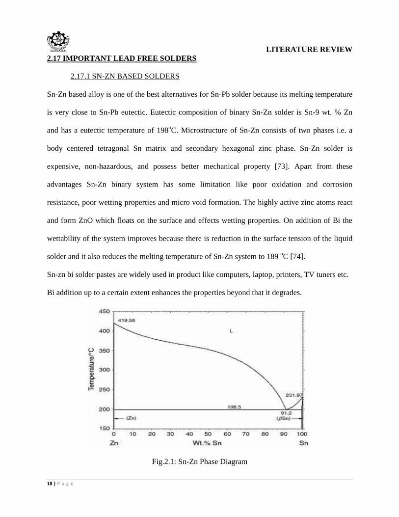
2.17 IMPORTANT LEAD FREE SOLDERS
2.17.1 SN-ZN BASED SOLDERS
Sn-Zn based alloy is one of the best alternatives for Sn-Pb solder because its melting temperature
is very close to Sn-Pb eutectic. Eutectic composition of binary Sn-Zn solder is Sn-9 wt. % Zn
and has a eutectic temperature of 198oC. Microstructure of Sn-Zn consists of two phases i.e. a
body centered tetragonal Sn matrix and secondary hexagonal zinc phase. Sn-Zn solder is
expensive, non-hazardous, and possess better mechanical property [73]. Apart from these
advantages Sn-Zn binary system has some limitation like poor oxidation and corrosion
resistance, poor wetting properties and micro void formation. The highly active zinc atoms react
and form ZnO which floats on the surface and effects wetting properties. On addition of Bi the
wettability of the system improves because there is reduction in the surface tension of the liquid
solder and it also reduces the melting temperature of Sn-Zn system to 189 oC [74].
Sn-zn bi solder pastes are widely used in product like computers, laptop, printers, TV tuners etc.
Bi addition up to a certain extent enhances the properties beyond that it degrades.
Fig.2.1: Sn-Zn Phase Diagram
LITERATURE REVIEW
19 | P a g e
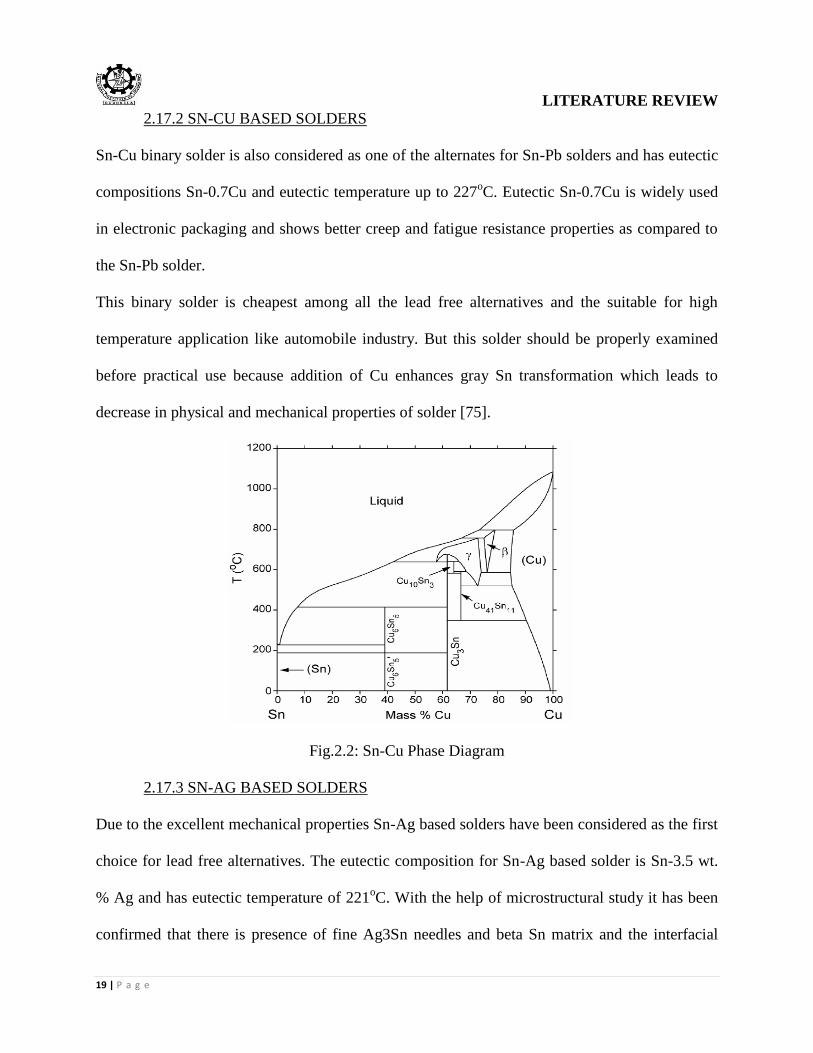
2.17.2 SN-CU BASED SOLDERS
Sn-Cu binary solder is also considered as one of the alternates for Sn-Pb solders and has eutectic
compositions Sn-0.7Cu and eutectic temperature up to 227oC. Eutectic Sn-0.7Cu is widely used
in electronic packaging and shows better creep and fatigue resistance properties as compared to
the Sn-Pb solder.
This binary solder is cheapest among all the lead free alternatives and the suitable for high
temperature application like automobile industry. But this solder should be properly examined
before practical use because addition of Cu enhances gray Sn transformation which leads to
decrease in physical and mechanical properties of solder [75].
Fig.2.2: Sn-Cu Phase Diagram
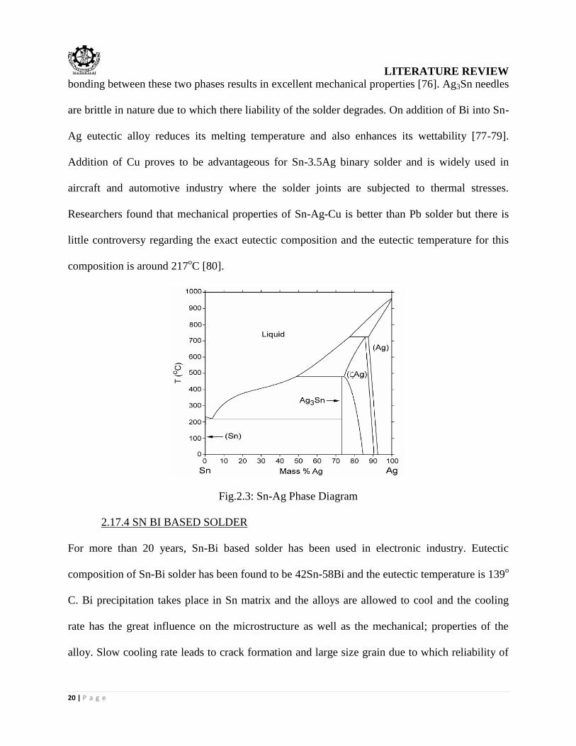
2.17.3 SN-AG BASED SOLDERS
Due to the excellent mechanical properties Sn-Ag based solders have been considered as the first
choice for lead free alternatives. The eutectic composition for Sn-Ag based solder is Sn-3.5 wt.
% Ag and has eutectic temperature of 221oC. With the help of microstructural study it has been
confirmed that there is presence of fine Ag3Sn needles and beta Sn matrix and the interfacial
LITERATURE REVIEW
20 | P a g e
bonding between these two phases results in excellent mechanical properties [76]. Ag3Sn needles
are brittle in nature due to which there liability of the solder degrades. On addition of Bi into Sn-
Ag eutectic alloy reduces its melting temperature and also enhances its wettability [77-79].
Addition of Cu proves to be advantageous for Sn-3.5Ag binary solder and is widely used in
aircraft and automotive industry where the solder joints are subjected to thermal stresses.
Researchers found that mechanical properties of Sn-Ag-Cu is better than Pb solder but there is
little controversy regarding the exact eutectic composition and the eutectic temperature for this
composition is around 217oC [80].
Fig.2.3: Sn-Ag Phase Diagram
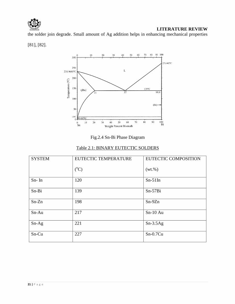
2.17.4 SN BI BASED SOLDER
For more than 20 years, Sn-Bi based solder has been used in electronic industry. Eutectic
composition of Sn-Bi solder has been found to be 42Sn-58Bi and the eutectic temperature is 139o
C. Bi precipitation takes place in Sn matrix and the alloys are allowed to cool and the cooling
rate has the great influence on the microstructure as well as the mechanical; properties of the
alloy. Slow cooling rate leads to crack formation and large size grain due to which reliability of
LITERATURE REVIEW
21 | P a g e
the solder join degrade. Small amount of Ag addition helps in enhancing mechanical properties
[81], [82].
Fig.2.4 Sn-Bi Phase Diagram
Table 2.1: BINARY EUTECTIC SOLDERS
SYSTEM EUTECTIC TEMPERATURE
(oC)
EUTECTIC COMPOSITION
(wt.%)
Sn- In 120 Sn-51In
Sn-Bi 139 Sn-57Bi
Sn-Zn 198 Sn-9Zn
Sn-Au 217 Sn-10 Au
Sn-Ag 221 Sn-3.5Ag
Sn-Cu 227 Sn-0.7Cu
LITERATURE REVIEW
22 | P a g e
2.18 SOLDERABILITY AND WETTABILITY
Solderability is the ability to achieve a clean metallic surface on which a molten solder can wet
properly [34]. In other words solderability is the ability of a surface to be wet by a molten solder
[83]. Solderability depends on several factors such as the type of flux, the type of solder and the
type of surface finish on which soldering will be performed.
The word wettability is basically same as soldering but it is often used as a quantitative measure
of solderability. The parameters such as contact angle, the meniscus rise, the capillary depth etc.
That can be obtained in soldering tests are often used as measures of the wettability of solders
[83]. Success of soldering depends on the wettability of the solder.
In general if wetting angle lies between 0o
to 90o proper wetting of substrate takes place. The
angle should be below 55o
for soldering purpose. Proper wetting will take place if there is net
decrease in total free energy at the interface. Surface tension of a liquid is a property which is
defined as the amount of energy needed to extend the liquid surface area on solid substrate.
Strength, reliability and degree of wetting are decided by this property [84], [85].
2.19 FORMATION OF INTERMETALLICS
Intermetallic compounds are formed when molten solder alloy reacts with a substrate. The most
common substrate used for electronic solders is Cu. Due to excellent conductivity Cu is widely
used in electronics and Sn- based solders readily wet it. Other potential, wettable substrates are
Ni/Fe alloys, Ag and Au, which are commonly coated over Cu contacts. Intermetallic
compounds (IMCs) are created when a molten solder wets either Cu or such alternative
substrates. They form while the solder is in a molten state but continue grow in the solid state at
room temperatures as well as elevated ones via a mechanism which requires diffusion. Strength
and wettability of a solder is determined by the formation and growth of interfacial layers.
LITERATURE REVIEW
23 | P a g e
Formation of intermetallic favor reliability of a solder joint, despite of this there are some
disadvantages. Intermetallic are brittle in nature and poor interfacial bonding is the result of
formation of thicker intermetallic layer. Soldering will not be successful if there is mismatch of
physical properties between substrate and intermetallic. Excessive growth of intermetallic leads
to degradation of solder joint strength, thermal fatigue life and fracture toughness of solder.
Formation of intermetallic depends upon the constituents of solder alloy and the manner in which
they react with the substrate. There can be a number of intermetallic compound formed but those
which are formed first during soldering process plays a vital role in wettability [86].
CHAPTER 3
EXPERIMENTAL
SETUP
&
METHODOLOGY
EXPERIMENTAL SETUP AND METHODOLOGY
24 | P a g e
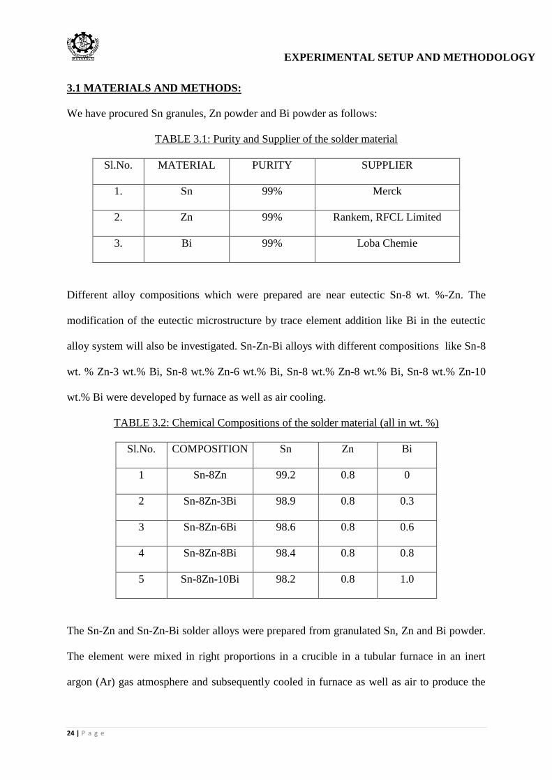
3.1 MATERIALS AND METHODS:
We have procured Sn granules, Zn powder and Bi powder as follows:
TABLE 3.1: Purity and Supplier of the solder material
Sl.No. MATERIAL PURITY SUPPLIER
1. Sn 99% Merck
2. Zn 99% Rankem, RFCL Limited
3. Bi 99% Loba Chemie
Different alloy compositions which were prepared are near eutectic Sn-8 wt. %-Zn. The
modification of the eutectic microstructure by trace element addition like Bi in the eutectic
alloy system will also be investigated. Sn-Zn-Bi alloys with different compositions like Sn-8
wt. % Zn-3 wt.% Bi, Sn-8 wt.% Zn-6 wt.% Bi, Sn-8 wt.% Zn-8 wt.% Bi, Sn-8 wt.% Zn-10
wt.% Bi were developed by furnace as well as air cooling.
TABLE 3.2: Chemical Compositions of the solder material (all in wt. %)
Sl.No. COMPOSITION Sn Zn Bi
1 Sn-8Zn 99.2 0.8 0
2 Sn-8Zn-3Bi 98.9 0.8 0.3
3 Sn-8Zn-6Bi 98.6 0.8 0.6
4 Sn-8Zn-8Bi 98.4 0.8 0.8
5 Sn-8Zn-10Bi 98.2 0.8 1.0
The Sn-Zn and Sn-Zn-Bi solder alloys were prepared from granulated Sn, Zn and Bi powder.
The element were mixed in right proportions in a crucible in a tubular furnace in an inert
argon (Ar) gas atmosphere and subsequently cooled in furnace as well as air to produce the
EXPERIMENTAL SETUP AND METHODOLOGY
25 | P a g e
solders. The furnace is heated to the desired temperature by electrical resistance heating
elements. Sn-Zn and Sn-Zn-Bi solder alloys have casting temperature in the range of 400oC
to 600oC. The molten alloy was held at this temperature for 2 hours. The morphology and
elemental composition of the samples were analysed using a JEOL JSM-6480LV scanning
electron microscope (SEM) equipped with an INCAPentaFET-x3 X-ray microanalysis
system with a high-angle ultra-thin window detector and a 30 mm2 Si(Li) crystal for EDS
(energy dispersive x-ray spectroscopy) analysis. The microstructure and various phases
formed were analysed. The near eutectic composition of Sn-8wt.% Zn was also air cooled
and the microstructures of the alloy was compared with the microstructure of the furnace
cooled sample. Differential scanning calorimetry (DSC) was done in order to determine the
melting point of the alloys. X-ray diffraction (XRD) of the alloys was done to found out if
any new phases were formed during their development. The tensile tests of the alloys were
also performed to find out their mechanical properties.
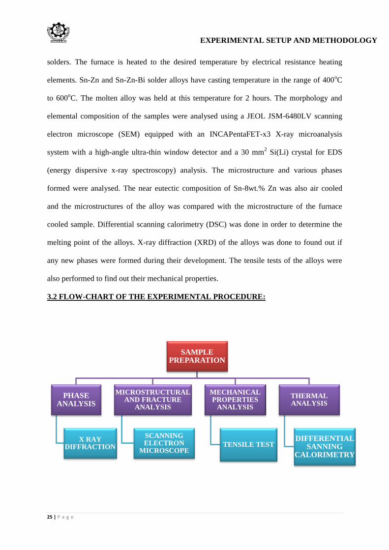
3.2 FLOW-CHART OF THE EXPERIMENTAL PROCEDURE:
SAMPLE PREPARATION
PHASE
ANALYSIS
X RAY DIFFRACTION
MICROSTRUCTURAL AND FRACTURE
ANALYSIS
SCANNING ELECTRON
MICROSCOPE
MECHANICAL PROPERTIES
ANALYSIS
TENSILE TEST
THERMAL ANALYSIS
DIFFERENTIAL SANNING
CALORIMETRY
EXPERIMENTAL SETUP AND METHODOLOGY
26 | P a g e
3.3 METALLOGRAPHY:
For microstructural studies, samples were cut approximately 8mm height. Samples were
ground roughly on a belt grinder. Now, samples were moved slowly up and back on the
surface of a flat belt grinder. After grinding samples were polished with the help of emery
papers. Emery papers contain different type of finer abrasive grains such as 1/0, 2/0, 3/0 and
4/0 grades. During each polishing operation the samples were moved perpendicular directions
to the existing scratches. After completion of polishing with the help of emery papers the
samples were polished by using rotating wheel covered with special cloths. Diamond paste
was used during polishing of samples on the cloths. Polishing operation was continued until
the surface of samples became plane and free from the nicks or inflection etc. Finally the
polished samples were cleaned thoroughly by the soap solution and dried subsequently with
the use of drier.
3.4 EXPERIMENTAL INSTRUMENTS:
3.4.1 TUBULAR FURNACE
Furnace is a device which is used for heating the samples. Source of heat energy to the
furnace is directly supplied by fuel combustion, by electricity in electric arc furnace and
through induction heating in induction furnace. Tubular furnace is electric heating furnace.
Temperature can be controlled via feedback from a thermocouple.
In this experiment work the elements such as Sn, Zn and Bi were in the right proportions.
These elements were heated in a crucible in tubular furnace in the presence of inert Argon
(Ar) gas atmosphere; the casting temperature is in the range of 400oC to 600
oC maintaining
the holding time as 2 h. Some samples were allowed to attain room temperature by air
cooling and some by furnace cooling.
EXPERIMENTAL SETUP AND METHODOLOGY
27 | P a g e
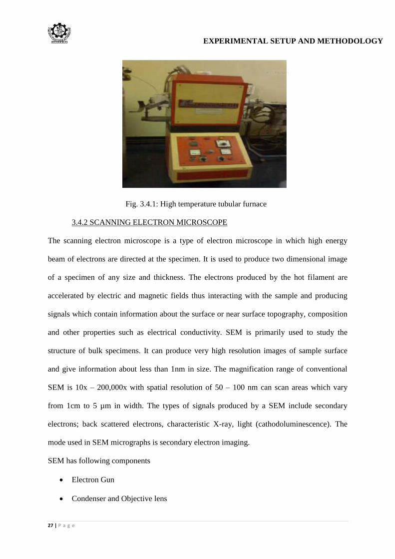
Fig. 3.4.1: High temperature tubular furnace
3.4.2 SCANNING ELECTRON MICROSCOPE
The scanning electron microscope is a type of electron microscope in which high energy
beam of electrons are directed at the specimen. It is used to produce two dimensional image
of a specimen of any size and thickness. The electrons produced by the hot filament are
accelerated by electric and magnetic fields thus interacting with the sample and producing
signals which contain information about the surface or near surface topography, composition
and other properties such as electrical conductivity. SEM is primarily used to study the
structure of bulk specimens. It can produce very high resolution images of sample surface
and give information about less than 1nm in size. The magnification range of conventional
SEM is 10x – 200,000x with spatial resolution of 50 – 100 nm can scan areas which vary
from 1cm to 5 µm in width. The types of signals produced by a SEM include secondary
electrons; back scattered electrons, characteristic X-ray, light (cathodoluminescence). The
mode used in SEM micrographs is secondary electron imaging.
SEM has following components
Electron Gun
Condenser and Objective lens
EXPERIMENTAL SETUP AND METHODOLOGY
28 | P a g e
Scan Coil
Aperture
Detectors and Display/Date Output devices
In the present work the solder samples work mechanically polish using standard
metallography techniques before the examination. The micrographs of the sample were
obtained. The mode used in SEM micrograph is secondary electron imaging.
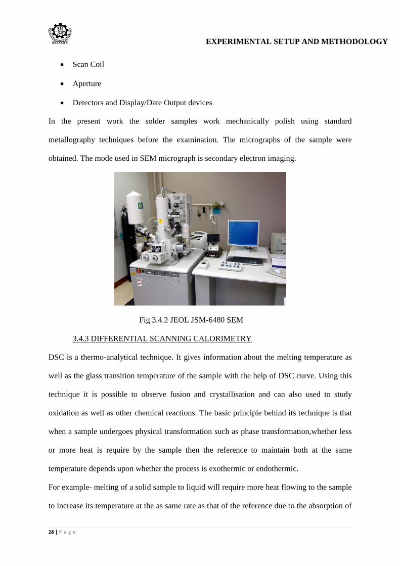
Fig 3.4.2 JEOL JSM‐6480 SEM
3.4.3 DIFFERENTIAL SCANNING CALORIMETRY
DSC is a thermo-analytical technique. It gives information about the melting temperature as
well as the glass transition temperature of the sample with the help of DSC curve. Using this
technique it is possible to observe fusion and crystallisation and can also used to study
oxidation as well as other chemical reactions. The basic principle behind its technique is that
when a sample undergoes physical transformation such as phase transformation,whether less
or more heat is require by the sample then the reference to maintain both at the same
temperature depends upon whether the process is exothermic or endothermic.
For example- melting of a solid sample to liquid will require more heat flowing to the sample
to increase its temperature at the as same rate as that of the reference due to the absorption of
EXPERIMENTAL SETUP AND METHODOLOGY
29 | P a g e
heat by the sample.Andthis undergoes endothermic phase transition from solid to liquid and if
the sample undergoes exothermic, less heat is required to raise the sample temperature such
as crystallisation. In this experimental work , we have taken the mass of solder 15mg ,
temprature range 25 oC to 300
oC and rate of temperature changes 10
oC per minute.
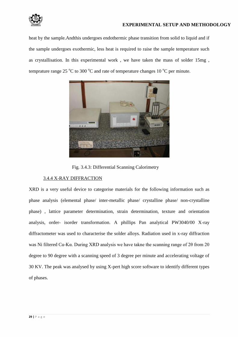
Fig. 3.4.3: Differential Scanning Calorimetry
3.4.4 X-RAY DIFFRACTION
XRD is a very useful device to categorise materials for the following information such as
phase analysis (elemental phase/ inter-metallic phase/ crystalline phase/ non-crystalline
phase) , lattice parameter determination, strain determination, texture and orientation
analysis, order- isorder transformation. A phillips Pan analytical PW3040/00 X-ray
diffractometer was used to characterise the solder alloys. Radiation used in x-ray diffraction
was Ni filtered Cu-Kα. During XRD analysis we have takne the scanning range of 2θ from 20
degree to 90 degree with a scanning speed of 3 degree per minute and accelerating voltage of
30 KV. The peak was analysed by using X-pert high score software to identify different types
of phases.
EXPERIMENTAL SETUP AND METHODOLOGY
30 | P a g e
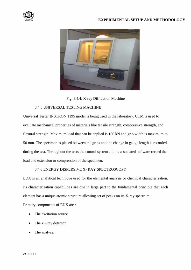
Fig. 3.4.4: X-ray Diffraction Machine
3.4.5 UNIVERSAL TESTING MACHINE
Universal Tester INSTRON 1195 model is being used in the laboratory. UTM is used to
evaluate mechanical properties of materials like tensile strength, compressive strength, and
flexural strength. Maximum load that can be applied is 100 kN and grip width is maximum to
50 mm. The specimen is placed between the grips and the change in gauge length is recorded
during the test. Throughout the tests the control system and its associated software record the
load and extension or compression of the specimen.
3.4.6 ENERGY DISPERSIVE X- RAY SPECTROSCOPY
EDX is an analytical technique used for the elemental analysis or chemical characterization.
Its characterization capabilities are due in large part to the fundamental principle that each
element has a unique atomic structure allowing set of peaks on its X-ray spectrum.
Primary components of EDX are :
The excitation source
The x – ray detector
The analyzer

CHAPTER 4
RESULT
&
DISCUSSION
RESULT AND DISCUSSION
31 | P a g e
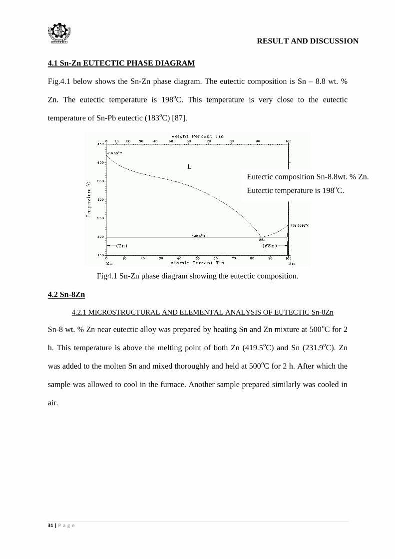
4.1 Sn-Zn EUTECTIC PHASE DIAGRAM
Fig.4.1 below shows the Sn-Zn phase diagram. The eutectic composition is Sn – 8.8 wt. %
Zn. The eutectic temperature is 198oC. This temperature is very close to the eutectic
temperature of Sn-Pb eutectic (183oC) [87].
Fig4.1 Sn-Zn phase diagram showing the eutectic composition.
4.2 Sn-8Zn
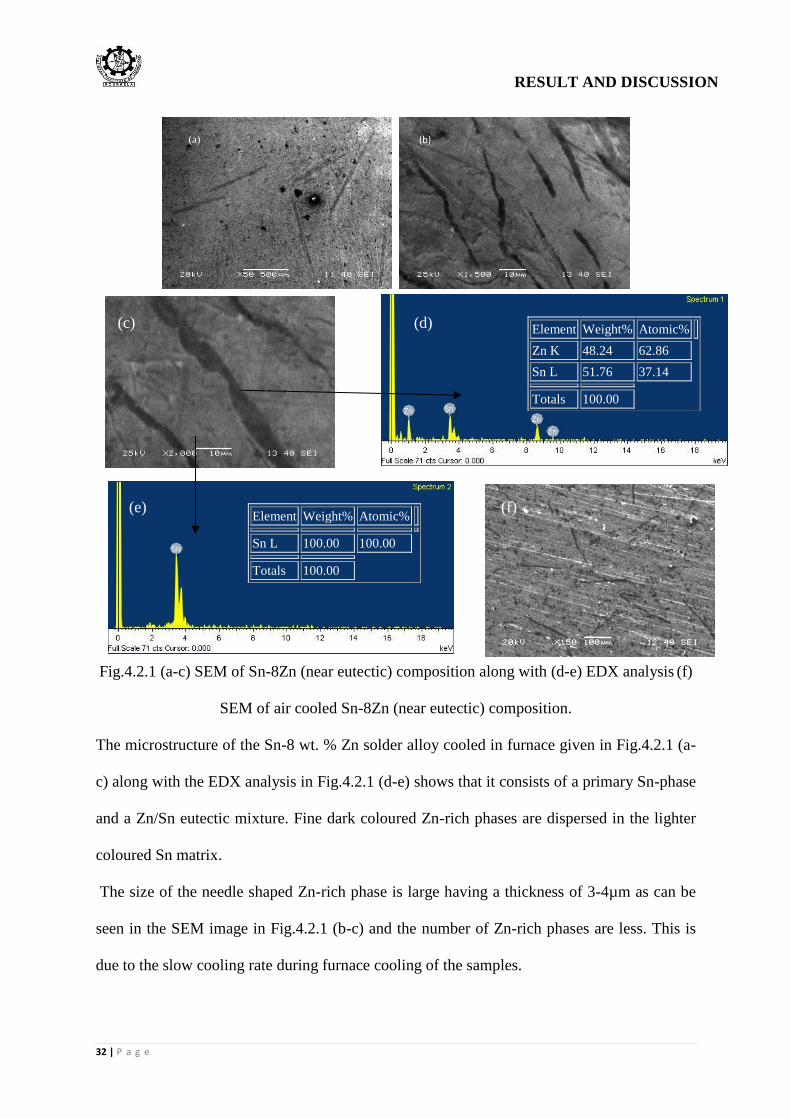
4.2.1 MICROSTRUCTURAL AND ELEMENTAL ANALYSIS OF EUTECTIC Sn-8Zn
Sn-8 wt. % Zn near eutectic alloy was prepared by heating Sn and Zn mixture at 500oC for 2
h. This temperature is above the melting point of both Zn (419.5oC) and Sn (231.9
oC). Zn
was added to the molten Sn and mixed thoroughly and held at 500oC for 2 h. After which the
sample was allowed to cool in the furnace. Another sample prepared similarly was cooled in
air.
Eutectic composition Sn-8.8wt. % Zn.
Eutectic temperature is 198oC.
RESULT AND DISCUSSION
32 | P a g e
Fig.4.2.1 (a-c) SEM of Sn-8Zn (near eutectic) composition along with (d-e) EDX analysis (f)
SEM of air cooled Sn-8Zn (near eutectic) composition.
The microstructure of the Sn-8 wt. % Zn solder alloy cooled in furnace given in Fig.4.2.1 (a-
c) along with the EDX analysis in Fig.4.2.1 (d-e) shows that it consists of a primary Sn-phase
and a Zn/Sn eutectic mixture. Fine dark coloured Zn-rich phases are dispersed in the lighter
coloured Sn matrix.
The size of the needle shaped Zn-rich phase is large having a thickness of 3-4µm as can be
seen in the SEM image in Fig.4.2.1 (b-c) and the number of Zn-rich phases are less. This is
due to the slow cooling rate during furnace cooling of the samples.
Element Weight% Atomic%
Zn K 48.24 62.86
Sn L 51.76 37.14
Totals 100.00
Element Weight% Atomic%
Sn L 100.00 100.00
Totals 100.00
(a) (b)
(c) (d)
(e) (f)
RESULT AND DISCUSSION
33 | P a g e
The lighter coloured Sn matrix is almost 100 % Sn containing no Zn at all whereas the dark
coloured Zn-rich phase contains both Zn and Sn (48.24 wt. % Zn and 51.76 wt. % Sn).
Fig.4.2.1 (f) shows the SEM image of near eutectic Sn-8Zn composition that has been cooled
in air. In this case the numbers of fine dark coloured Zn-rich phases dispersed in the lighter
coloured Sn matrix are large in number and are also finer in size (1-2µm).
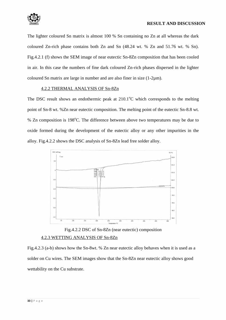
4.2.2 THERMAL ANALYSIS OF Sn-8Zn
The DSC result shows an endothermic peak at 210.1oC which corresponds to the melting
point of Sn-8 wt. %Zn near eutectic composition. The melting point of the eutectic Sn-8.8 wt.
% Zn composition is 198oC. The difference between above two temperatures may be due to
oxide formed during the development of the eutectic alloy or any other impurities in the
alloy. Fig.4.2.2 shows the DSC analysis of Sn-8Zn lead free solder alloy.
Fig.4.2.2 DSC of Sn-8Zn (near eutectic) composition
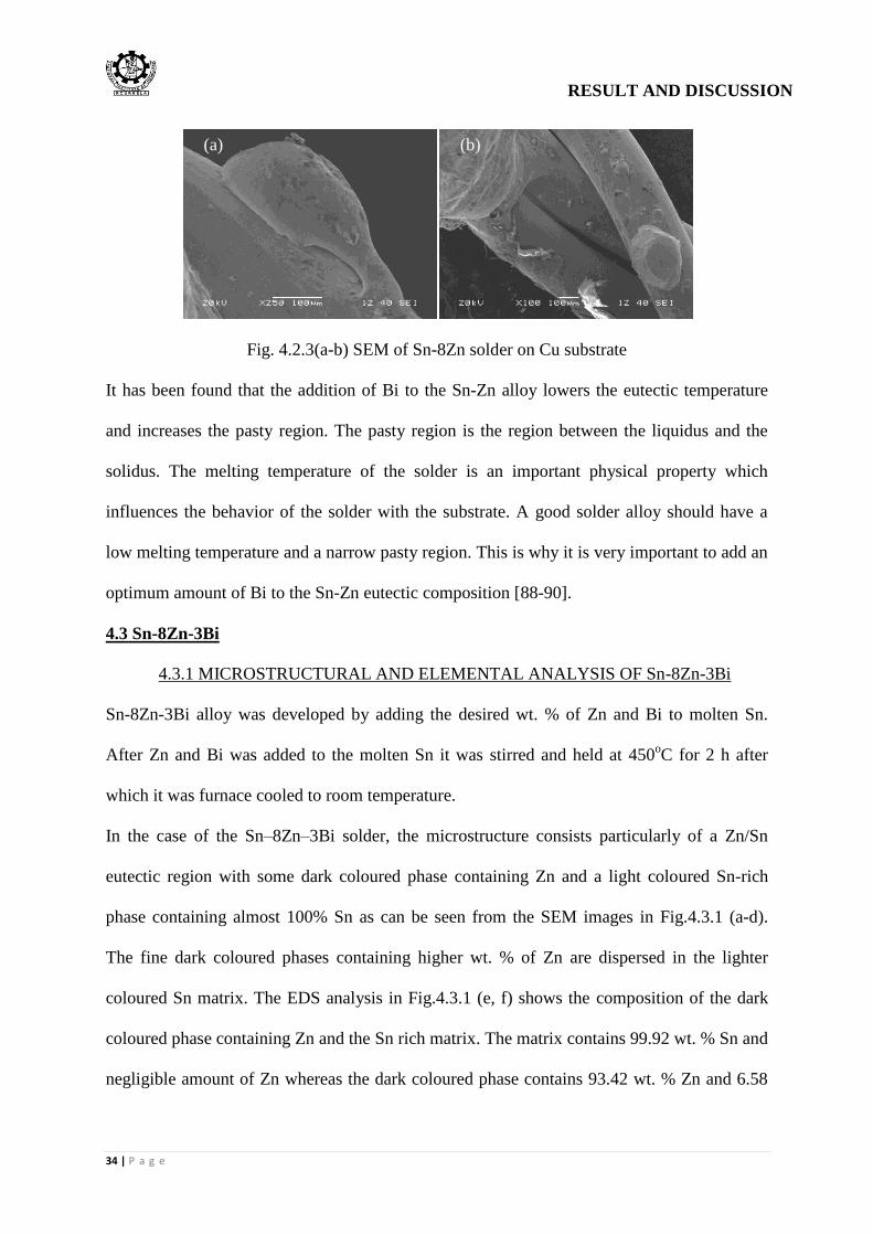
4.2.3 WETTING ANALYSIS OF Sn-8Zn
Fig.4.2.3 (a-b) shows how the Sn-8wt. % Zn near eutectic alloy behaves when it is used as a
solder on Cu wires. The SEM images show that the Sn-8Zn near eutectic alloy shows good
wettability on the Cu substrate.
RESULT AND DISCUSSION
34 | P a g e
Fig. 4.2.3(a-b) SEM of Sn-8Zn solder on Cu substrate
It has been found that the addition of Bi to the Sn-Zn alloy lowers the eutectic temperature
and increases the pasty region. The pasty region is the region between the liquidus and the
solidus. The melting temperature of the solder is an important physical property which
influences the behavior of the solder with the substrate. A good solder alloy should have a
low melting temperature and a narrow pasty region. This is why it is very important to add an
optimum amount of Bi to the Sn-Zn eutectic composition [88-90].
4.3 Sn-8Zn-3Bi
4.3.1 MICROSTRUCTURAL AND ELEMENTAL ANALYSIS OF Sn-8Zn-3Bi
Sn-8Zn-3Bi alloy was developed by adding the desired wt. % of Zn and Bi to molten Sn.
After Zn and Bi was added to the molten Sn it was stirred and held at 450oC for 2 h after
which it was furnace cooled to room temperature.
In the case of the Sn–8Zn–3Bi solder, the microstructure consists particularly of a Zn/Sn
eutectic region with some dark coloured phase containing Zn and a light coloured Sn-rich
phase containing almost 100% Sn as can be seen from the SEM images in Fig.4.3.1 (a-d).
The fine dark coloured phases containing higher wt. % of Zn are dispersed in the lighter
coloured Sn matrix. The EDS analysis in Fig.4.3.1 (e, f) shows the composition of the dark
coloured phase containing Zn and the Sn rich matrix. The matrix contains 99.92 wt. % Sn and
negligible amount of Zn whereas the dark coloured phase contains 93.42 wt. % Zn and 6.58
(a) (b)
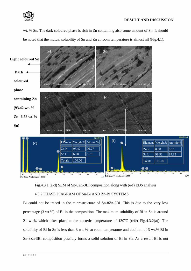
RESULT AND DISCUSSION
35 | P a g e
wt. % Sn. The dark coloured phase is rich in Zn containing also some amount of Sn. It should
be noted that the mutual solubility of Sn and Zn at room temperature is almost nil (Fig.4.1).
Fig.4.3.1 (a-d) SEM of Sn-8Zn-3Bi composition along with (e-f) EDS analysis
4.3.2 PHASE DIAGRAM OF Sn-Bi AND Zn-Bi SYSTEMS
Bi could not be traced in the microstructure of Sn-8Zn-3Bi. This is due to the very low
percentage (3 wt.%) of Bi in the composition. The maximum solubility of Bi in Sn is around
21 wt.% which takes place at the euctetic temperature of 139oC (refer Fig.4.3.2(a)). The
solubility of Bi in Sn is less than 3 wt. % at room temperature and addition of 3 wt.% Bi in
Sn-8Zn-3Bi composition possibly forms a solid solution of Bi in Sn. As a result Bi is not
Element Weight% Atomic%
Zn K 93.42 96.27
Sn L 6.58 3.73
Totals 100.00
Element Weight% Atomic%
Zn K 0.08 0.15
Sn L 99.92 99.85
Totals 100.00
Dark
coloured
phase
containing Zn
(93.42 wt. %
Zn- 6.58 wt.%
Sn)
Light coloured Sn
rich region
(a) (b)
(c) (d)
(e) (f)
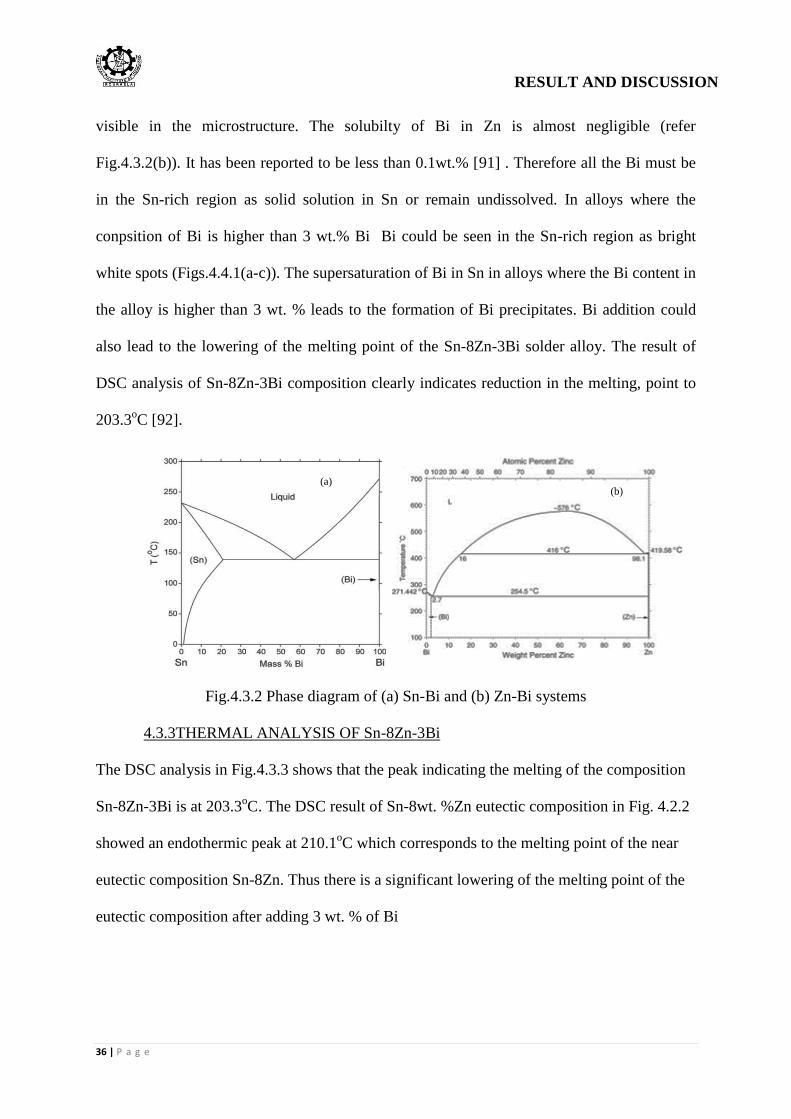
RESULT AND DISCUSSION
36 | P a g e
visible in the microstructure. The solubilty of Bi in Zn is almost negligible (refer
Fig.4.3.2(b)). It has been reported to be less than 0.1wt.% [91] . Therefore all the Bi must be
in the Sn-rich region as solid solution in Sn or remain undissolved. In alloys where the
conpsition of Bi is higher than 3 wt.% Bi Bi could be seen in the Sn-rich region as bright
white spots (Figs.4.4.1(a-c)). The supersaturation of Bi in Sn in alloys where the Bi content in
the alloy is higher than 3 wt. % leads to the formation of Bi precipitates. Bi addition could
also lead to the lowering of the melting point of the Sn-8Zn-3Bi solder alloy. The result of
DSC analysis of Sn-8Zn-3Bi composition clearly indicates reduction in the melting, point to
203.3oC [92].
Fig.4.3.2 Phase diagram of (a) Sn-Bi and (b) Zn-Bi systems
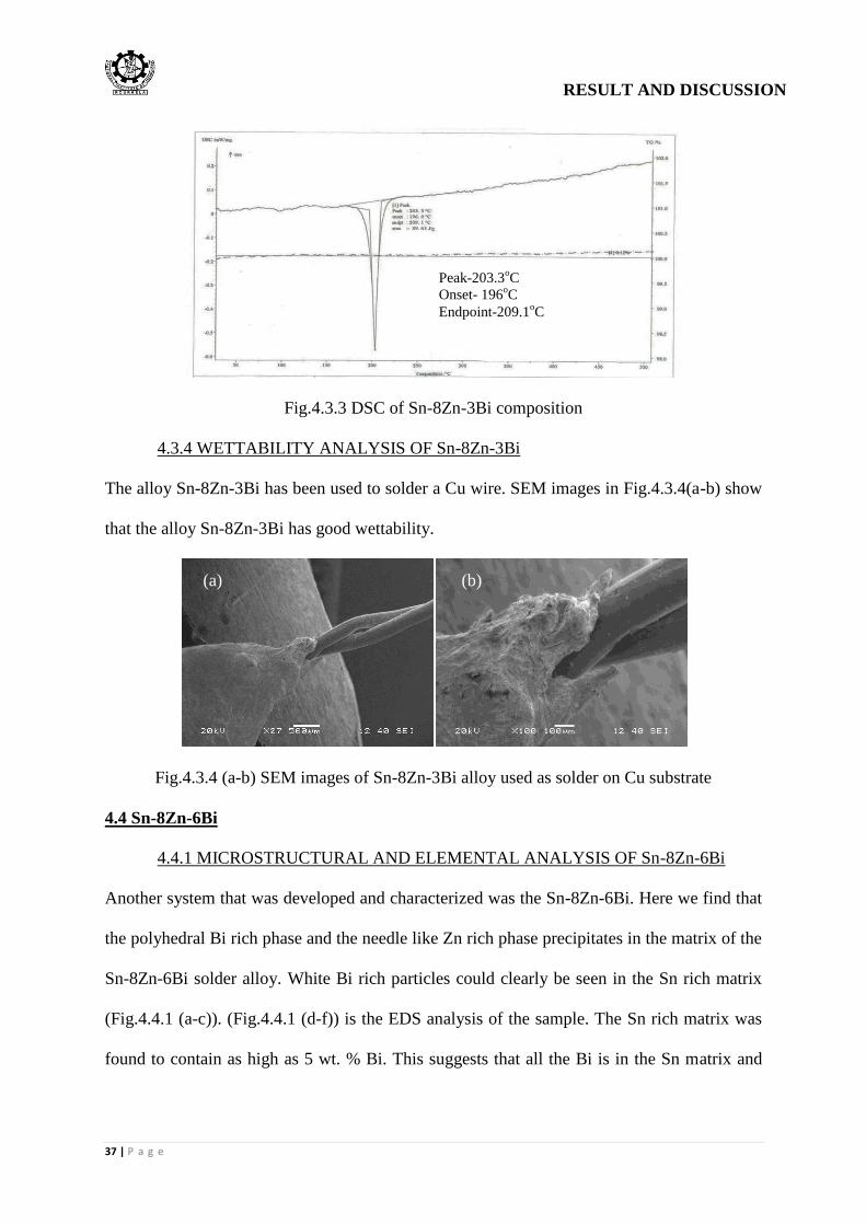
4.3.3THERMAL ANALYSIS OF Sn-8Zn-3Bi
The DSC analysis in Fig.4.3.3 shows that the peak indicating the melting of the composition
Sn-8Zn-3Bi is at 203.3oC. The DSC result of Sn-8wt. %Zn eutectic composition in Fig. 4.2.2
showed an endothermic peak at 210.1oC which corresponds to the melting point of the near
eutectic composition Sn-8Zn. Thus there is a significant lowering of the melting point of the
eutectic composition after adding 3 wt. % of Bi
(a) (b)
RESULT AND DISCUSSION
37 | P a g e
Fig.4.3.3 DSC of Sn-8Zn-3Bi composition
4.3.4 WETTABILITY ANALYSIS OF Sn-8Zn-3Bi
The alloy Sn-8Zn-3Bi has been used to solder a Cu wire. SEM images in Fig.4.3.4(a-b) show
that the alloy Sn-8Zn-3Bi has good wettability.
Fig.4.3.4 (a-b) SEM images of Sn-8Zn-3Bi alloy used as solder on Cu substrate
4.4 Sn-8Zn-6Bi
4.4.1 MICROSTRUCTURAL AND ELEMENTAL ANALYSIS OF Sn-8Zn-6Bi
Another system that was developed and characterized was the Sn-8Zn-6Bi. Here we find that
the polyhedral Bi rich phase and the needle like Zn rich phase precipitates in the matrix of the
Sn-8Zn-6Bi solder alloy. White Bi rich particles could clearly be seen in the Sn rich matrix
(Fig.4.4.1 (a-c)). (Fig.4.4.1 (d-f)) is the EDS analysis of the sample. The Sn rich matrix was
found to contain as high as 5 wt. % Bi. This suggests that all the Bi is in the Sn matrix and
Peak-203.3oC
Onset- 196oC
Endpoint-209.1oC
(a) (b)
RESULT AND DISCUSSION
38 | P a g e
they can be seen as white particles in certain areas of the Sn matrix as the maximum
solubility of Bi in Sn is only 3 wt.% and the alloy contains 6 wt.% Bi.
The Zn containing phases are dark in colour the Sn-rich matrix phase is light coloured and the
Bi containing particles is white in colour. Here Bi could be seen in the microstructure as 6
wt. % is added. Some voids are also observed at the surface of the Sn–8Zn-6Bi solder alloys.
The diffusion of Zn leads to vacancy diffusion in the opposite direction and the accumulation
of vacancies lead to void formation.
Fig.4.4.1 (a-c) SEM images of Sn-8Zn-6Bi alloy (d-f) EDX analysis of various regions in Sn-
8Zn-6Bi alloy
Element Weight% Atomic%
Zn K 0.02 0.04
Sn L 94.96 97.05
Bi M 5.02 2.91
Totals 100.00
Element Weight% Atomic%
Zn K 20.45 32.41
Sn L 74.59 65.13
Bi M 4.96 2.46
Totals 100.00
Element Weight% Atomic%
Zn K 11.42 19.04
Sn L 87.60 80.45
Bi M 0.98 0.51
Totals 100.00
Zn
Sn
(a) (b)
(c) (d)
(e) (f)
Light coloured
Sn-rich matrix Dark coloured
Zn containing
region
Bi-rich particle
RESULT AND DISCUSSION
39 | P a g e
4.4.2 THERMAL ANALYSIS OF Sn-8Zn-6Bi
The DSC analysis of Sn-8Zn-6Bi alloy is given in Fig.4.4.2. The melting point of the alloy
Sn-8Zn-6Bi has been found to be 201.24oC. There is a slight decrease in the melting point
with the increase in the wt.% of Bi in the alloy.
Fig.4.4.2 DSC of Sn-8Zn-6Bi Composition
4.4.3 WETTING ANALYSIS OF Sn-8ZN-6Bi
The SEM images in Fig.4.4.3(a-b) does not show very good wettability between the solder
and the Cu wire.
Fig.4.4.3 (a-b) SEM images of Sn-8Zn-6Bi alloy used as solder on Cu wire
4.5 Sn-8Zn-8Bi
4.5.1 MICROSTUCTURAL AND ELEMENTAL ANALYSIS OF Sn-8Zn-8Bi
Sn-8Zn-8Bi alloys showed a large number of white spots. This is seen in the SEM images in
Fig.4.5.1 (a-c). These are Bi rich particles which have precipitated in the Sn rich matrix and
(a) (b)
RESULT AND DISCUSSION
40 | P a g e
the contained about 7.82 wt. % Bi. The amount of Bi in the light coloured Sn rich matrix is
5.81 wt. %. It is known that the solubility of Bi in Zn is less than 0.1 wt. %. This can be seen
in the phase diagram in Fig. 4.3.2(b). Bi could not be found in the dark coloured Zn
containing region. These regions contain 13.49 wt. % Zn and 86.51 wt. % Sn. The light
coloured matrix is found to contain only 0.02 wt. % Zn.
Fig.4.5.1 (a-c) SEM image of Sn-8Zn-8Bi alloy (d-f) EDX analysis of the various regions in
the sample
Element Weight% Atomic%
Zn K 33.98 49.62
Sn L 58.20 46.81
Bi M 7.82 3.57
Totals 100.00
Element Weight% Atomic%
Zn K 13.49 22.06
Sn L 86.51 77.94
Totals 100.00
Element Weight% Atomic%
Zn K 12.35 20.84
Sn L 81.85 76.09
Bi M 5.81 3.07
Totals 100.00
(a) (b)
(c) (d)
(e) (f)
RESULT AND DISCUSSION
41 | P a g e
4.5.2 THERMAL ANALYSIS OF Sn-8Zn-8Bi
The DSC analysis of Sn-8Zn-8Bi alloy is given in Fig.4.5.2. The melting point of the alloy
Sn-8Zn-8Bi has been found to be 201.42oC. There is a slight increase in the melting point
with the increase in the wt.% of Bi in the alloy. Further addition of Bi to the near eutectic
compsoiton of Sn-8Zn does not decrease the melting point of the alloy
Fig.4.5.2 DSC of Sn-8Zn-8Bi Composition
4.5.3 WETTABILITY ANALYSIS OF Sn-8Zn-8Bi
Sn-8Zn-8Bi alloy was also used to solder Cu wire to find out its wettability. The wettability
of this alloy seems poorer than the Sn-8Zn-6Bi alloy. The Sn-Zn-Bi alloys are definitely
capable to replace Sn-Pb solder due to its low melting temperature and low cost but the
wettability of this alloy is not as good as the Sn-Pb alloy. The compositions of the alloy
containing higher Bi wt. % has poorer wettability.
Fig.4.5.3 (a-b) SEM images of Sn-8Zn-8Bi alloy used as solder on Cu wire
(a) (b)
RESULT AND DISCUSSION
42 | P a g e
4.6 Sn-8Zn-10Bi
4.6.1 MICROSTRUCTURAL AND ELEMENTAL ANALYSIS OF Sn-8Zn-10Bi
The microstructure of Sn-8Zn-10Bi is similar to the Sn-8Zn-8Bi alloys but the white Bi rich
regions contained a higher percentage of Bi. The Bi wt. % is found to be 25.24 in the Bi rich
region. The microstructure is shown is in Fig.4.6.1 (a-c) along with EDS analysis in Fig.4.6.1
(d-f)
.
Fig.4.6.1 (a-c) SEM images of Sn-8Zn-10Bi alloy (d-f) EDX of various regions in the SEM
image
Element Weight% Atomic%
O K 18.80 60.97
Zn L 9.89 7.85
Sn L 71.31 31.17
Totals 100.00
Element Weight% Atomic%
O K 5.15 31.27
Zn L 0.14 0.21
Sn L 69.46 56.80
Bi M 25.24 11.72
Totals 100.00
(a)
(b)
(c)
(d)
(e)
(f)

RESULT AND DISCUSSION
43 | P a g e
The light coloured regions are Sn rich regions having almost no Zn or Bi in it. The dark areas
contain higher wt.% of Zn (9.89 wt.%) although they contain significant amount of Sn(71.31
wt.%). The white spots have been identified to be Bi rich and having significant percentage
of Sn in it. EDS analysis shows that there is also some amount of oxygen. Bi tries to
agglomerate around the Zn-rich phase. The eutectic mixtures are found to be layer type.
4.6.2 WETTA BILITY ANALYSIS OF Sn-8Zn-10Bi
Fig.4.6.2 (a-b) shows the SEM images of soldering of Sn-8Zn-10Bi with Cu wires. There
seem to a less wettability of the alloy on the Cu surface.
Fig. 4.6.2(a-b) SEM images of Sn-8Zn-10Bi alloy used for soldering Cu wires
4.7 X-RAY DIFFRACTION ANALYSIS
The x-ray diffraction plots of the various solder alloys in Fig.4.7 suggest that no new phase
has been formed. The phase diagrams of Sn-Zn in Fig.4.1 and Sn-Bi and Zn-Bi in
Figs.4.3.2(a-b) also suggest that no new phase formation takes place between the three
elements Sn, Zn and Bi.
(b) (a)
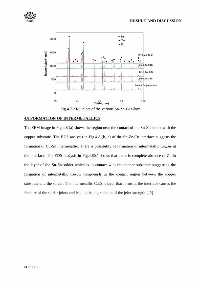
RESULT AND DISCUSSION
44 | P a g e
Fig.4.7 XRD plots of the various Sn-Zn-Bi alloys
4.8 FORMATION OF INTERMETALLICS
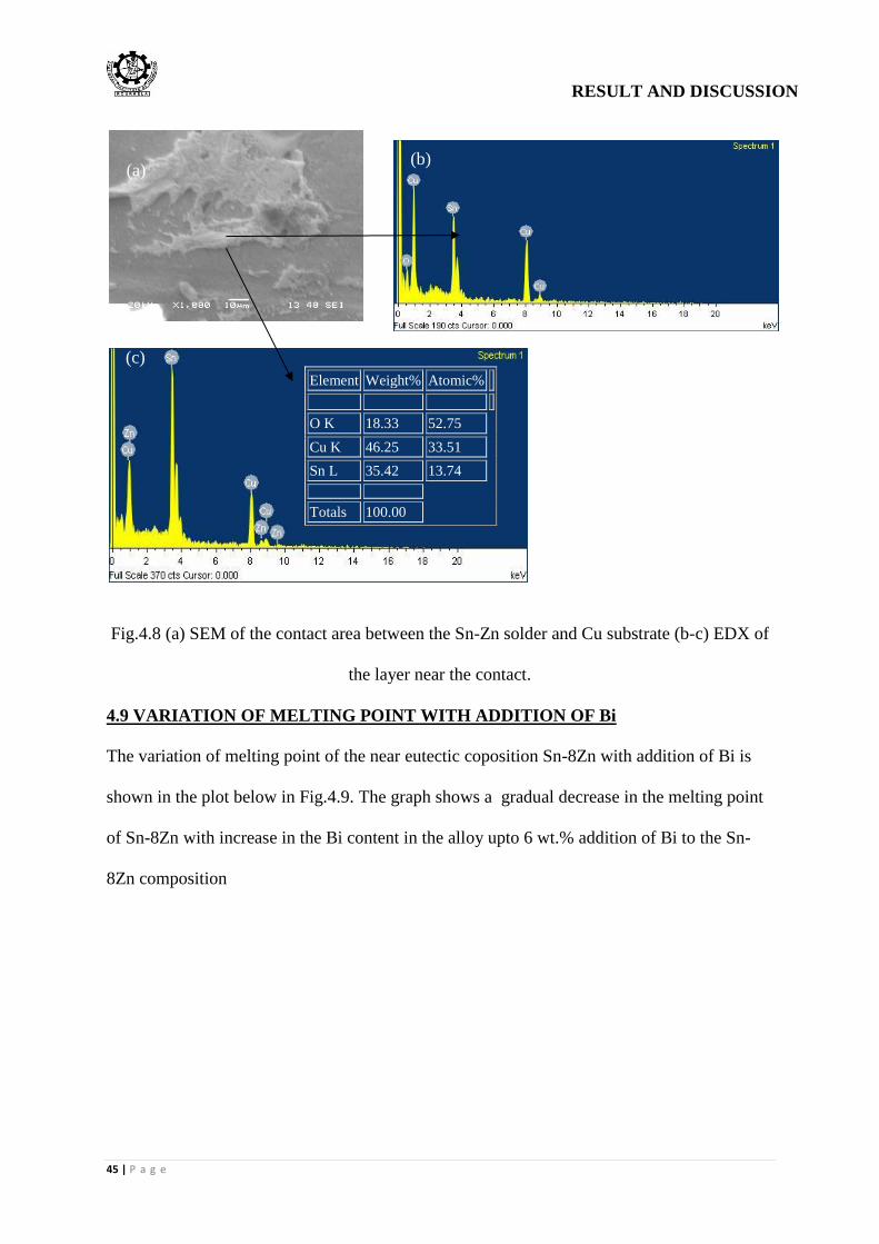
The SEM image in Fig.4.8 (a) shows the region near the contact of the Sn-Zn solder with the
copper substrate. The EDS analysis in Fig.4.8 (b, c) of the Sn-Zn/Cu interface suggests the
formation of Cu-Sn intermetallic. There is possibility of formation of intermetallic Cu6Sn5 at
the interface. The EDS analysis in Fig.4.8(c) shows that there is complete absence of Zn in
the layer of the Sn-Zn solder which is in contact with the copper substrate suggesting the
formation of intermetallic Cu-Sn compounds in the contact region between the copper
substrate and the solder. The intermetallic Cu6Sn5 layer that forms at the interface causes the
fracture of the solder joints and lead to the degradation of the joint strength [12].
RESULT AND DISCUSSION
45 | P a g e
Fig.4.8 (a) SEM of the contact area between the Sn-Zn solder and Cu substrate (b-c) EDX of
the layer near the contact.
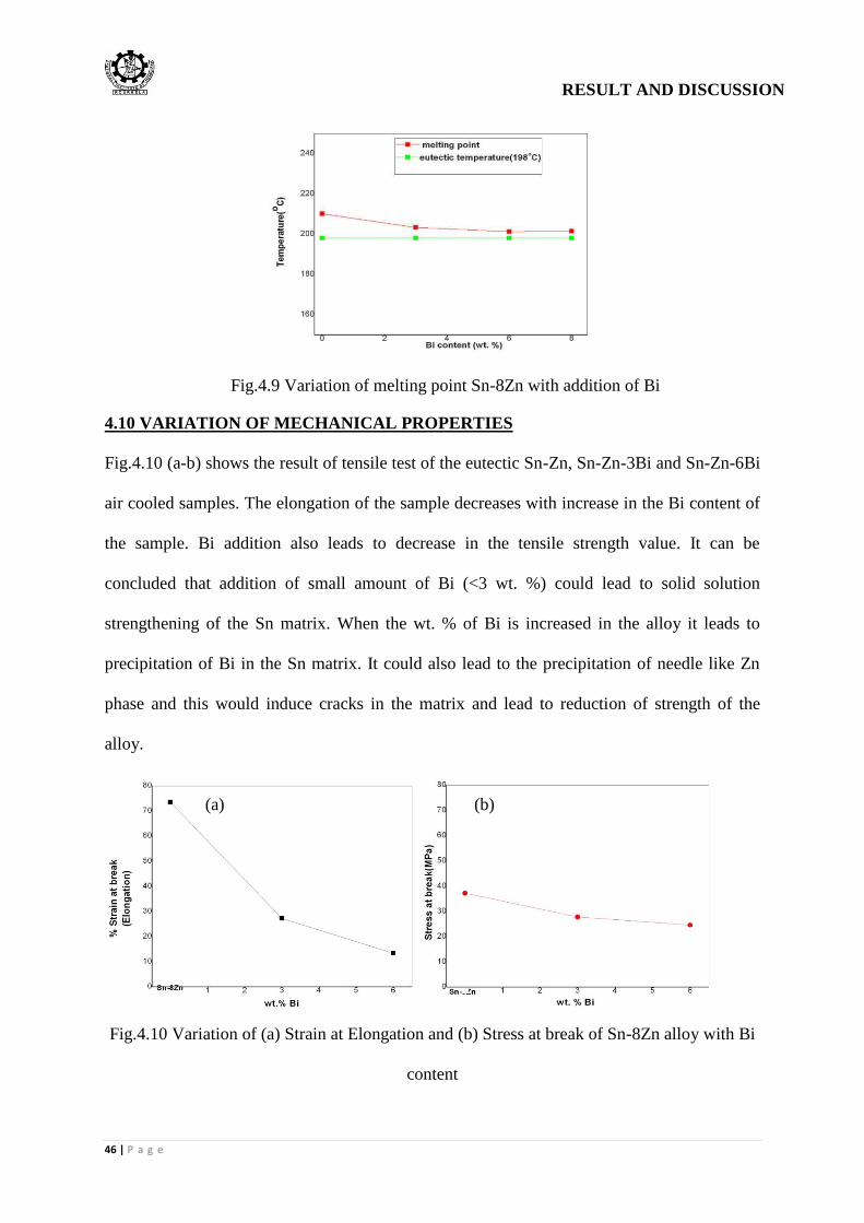
4.9 VARIATION OF MELTING POINT WITH ADDITION OF Bi
The variation of melting point of the near eutectic coposition Sn-8Zn with addition of Bi is
shown in the plot below in Fig.4.9. The graph shows a gradual decrease in the melting point
of Sn-8Zn with increase in the Bi content in the alloy upto 6 wt.% addition of Bi to the Sn-
8Zn composition
Element Weight% Atomic%
O K 18.33 52.75
Cu K 46.25 33.51
Sn L 35.42 13.74
Totals 100.00
(a) (b)
(c)
RESULT AND DISCUSSION
46 | P a g e
Fig.4.9 Variation of melting point Sn-8Zn with addition of Bi
4.10 VARIATION OF MECHANICAL PROPERTIES
Fig.4.10 (a-b) shows the result of tensile test of the eutectic Sn-Zn, Sn-Zn-3Bi and Sn-Zn-6Bi
air cooled samples. The elongation of the sample decreases with increase in the Bi content of
the sample. Bi addition also leads to decrease in the tensile strength value. It can be
concluded that addition of small amount of Bi (<3 wt. %) could lead to solid solution
strengthening of the Sn matrix. When the wt. % of Bi is increased in the alloy it leads to
precipitation of Bi in the Sn matrix. It could also lead to the precipitation of needle like Zn
phase and this would induce cracks in the matrix and lead to reduction of strength of the
alloy.
Fig.4.10 Variation of (a) Strain at Elongation and (b) Stress at break of Sn-8Zn alloy with Bi
content
(a) (b)

RESULT AND DISCUSSION
47 | P a g e
4.11 FRACTOGRAPHY
Fig.4.11 shows the SEM images of the fracture surface of the three Sn-8Zn, Sn-8Zn-3Bi and
Sn-8Zn-6Bi tensile specimens. All the alloys show a ductile fracture with dimples on the
fracture surface. In the case of Sn-8Zn-6Bi (Fig.4.11 (e,f)) the cup and cone fracture size is
found to be larger as compared to the Sn-8Zn (Fig.4.11(a,b)) and Sn-8Zn-3Bi (Fig.4.11(c,d))
alloy. This suggests the lowering of ductility of the alloy with addition of higher wt. % of Bi.
Sn-8Zn and Sn-8Zn-3Bi show smaller cup and cone fracture size. This suggests ductile
failure in these alloys.
Fig.4.11 SEM images of the fracture surfaces of (a,b) Sn-8Zn (c,d) Sn-8Zn-3Bi (e,f) Sn-8Zn-
6Bi alloys
(a) (b)
(c) (d)
(e) (f)
RESULT AND DISCUSSION
48 | P a g e
4.12 Sn-Zn-Ag
. We have procured Sn granules, Zn powder and Ag powder as follows:
TABLE 4.12: Purity and Supplier of the solder material
Sl.No. MATERIAL PURITY SUPPLIER
1. Sn 99% Merck
2. Zn 99% Rankem, RFCL Limited
3. Ag 99% Loba Chemie
Different alloy compositions which were prepared are near eutectic Sn-8 wt. %-Zn. The
modification of the eutectic microstructure by trace element addition like Ag in the eutectic
alloy system will also be investigated. Sn-Zn-Ag alloys with different compositions like Sn-8
wt. % Zn-0.05 wt. %Ag, Sn-8 wt. % Zn-0.1 wt. %Ag and Sn-8 wt. % Zn-0.2 wt. %Ag were
developed by furnace cooling.
TABLE 4.13 : Chemical Compositions of the solder material (all in wt. %)
Sl.No. COMPOSITION Sn Zn Bi
1 Sn-8Zn 99.2 0.8 0
2 Sn-8Zn-0.05Ag 98.9 0.8 0.3
3 Sn-8Zn-0.1Ag 98.6 0.8 0.6
4 Sn-8Zn-0.2Ag 98.4 0.8 0.8
The Sn-Zn and Sn-Zn-Ag solder alloys were prepared from granulated Sn, Zn and Ai powder.
The element were mixed in right proportions in a crucible in a tubular furnace in an inert
argon (Ar) gas atmosphere and subsequently cooled in furnace to produce the solders. The
furnace is heated to the desired temperature by electrical resistance heating elements. Sn-Zn
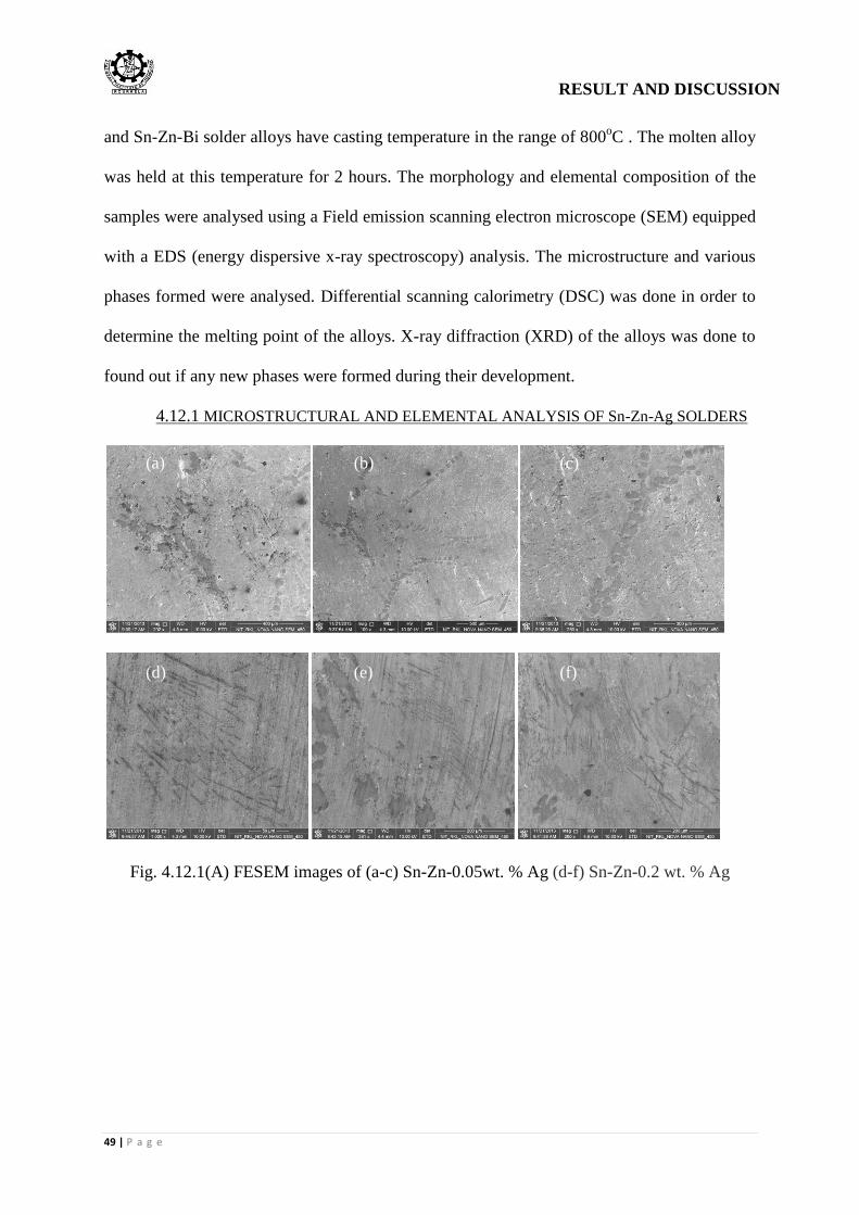
RESULT AND DISCUSSION
49 | P a g e
and Sn-Zn-Bi solder alloys have casting temperature in the range of 800oC . The molten alloy
was held at this temperature for 2 hours. The morphology and elemental composition of the
samples were analysed using a Field emission scanning electron microscope (SEM) equipped
with a EDS (energy dispersive x-ray spectroscopy) analysis. The microstructure and various
phases formed were analysed. Differential scanning calorimetry (DSC) was done in order to
determine the melting point of the alloys. X-ray diffraction (XRD) of the alloys was done to
found out if any new phases were formed during their development.
4.12.1 MICROSTRUCTURAL AND ELEMENTAL ANALYSIS OF Sn-Zn-Ag SOLDERS
Fig. 4.12.1(A) FESEM images of (a-c) Sn-Zn-0.05wt. % Ag (d-f) Sn-Zn-0.2 wt. % Ag
(a) (b) (c)
(f) (e) (d)
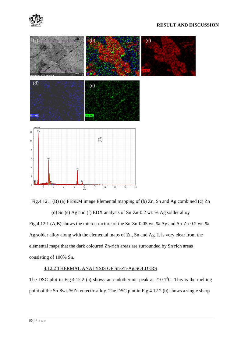
RESULT AND DISCUSSION
50 | P a g e
Fig.4.12.1 (B) (a) FESEM image Elemental mapping of (b) Zn, Sn and Ag combined (c) Zn
(d) Sn (e) Ag and (f) EDX analysis of Sn-Zn-0.2 wt. % Ag solder alloy
Fig.4.12.1 (A,B) shows the microstructure of the Sn-Zn-0.05 wt. % Ag and Sn-Zn-0.2 wt. %
Ag solder alloy along with the elemental maps of Zn, Sn and Ag. It is very clear from the
elemental maps that the dark coloured Zn-rich areas are surrounded by Sn rich areas
consisting of 100% Sn.
4.12.2 THERMAL ANALYSIS OF Sn-Zn-Ag SOLDERS
The DSC plot in Fig.4.12.2 (a) shows an endothermic peak at 210.1oC. This is the melting
point of the Sn-8wt. %Zn eutectic alloy. The DSC plot in Fig.4.12.2 (b) shows a single sharp
(a) (b) (c)
(d) (e)
2 4 6 8 10 12 14 16 18 20
keV
0
2
4
6
8
10
12
cps/eV
Zn
Zn
Zn
Ag
Ag
Ag
Sn
Sn Sn
(f)

RESULT AND DISCUSSION
51 | P a g e
endothermic peak at 215.48oC This corresponds to the melting point the Sn-Zn-0.05Ag. The
melting point the Sn-Zn-0.05Ag is slightly higher than the eutectic point of Sn-Zn system
The DSC of Sn-Zn-0.1Ag solder alloy in Fig.4.12.2(c) shows that the melting point of the
alloy is 198.7oC. Thus there is a reduction in the melting point of the eutectic composition
after addition of 0.1 wt. % Ag but instead of a single sharp peak now can see two peaks. This
is due to the addition of Ag. The liquidus line of the Sn-Zn eutectic alloy rises with the
increase of the Ag content in the alloy. This leads to an increase in the pasty region. It can be
noted that the height of the first peak decreases with an increase in the Ag content in the
alloy. The shoulder was observed at around 220oC in the DSC curves for 0.1 and 0.2 wt. %
Ag alloys (Figs.4.12.2(c) and (d)). This shoulder is not present 0.05 wt. % Ag containing
solders. The addition of a large amount of Ag in the Sn-Zn-0.1Ag and Sn-Zn-0.2Ag alloys
resulted in the formation of larger amount of Ag3Zn intermetallic compound. This reaction
reduced the Zn content of the eutectic Sn-Zn composition which resulted in the formation of
a hypoeutectic β-Sn structure. This is why the DSC plots of the solder alloys Sn-Zn-0.1Ag
and Sn-Zn-0.2Ag showed two endothermic peaks. The first endothermic peak represents the
melting of the eutectic Sn-Zn-Ag ternary system and the other peak is due to the melting of
the hypoeutectic β-Sn [93-95].
Peak-210.1oC
Onset- 199.2oC
Endpoint-216.2oC
(a) (b) (b)
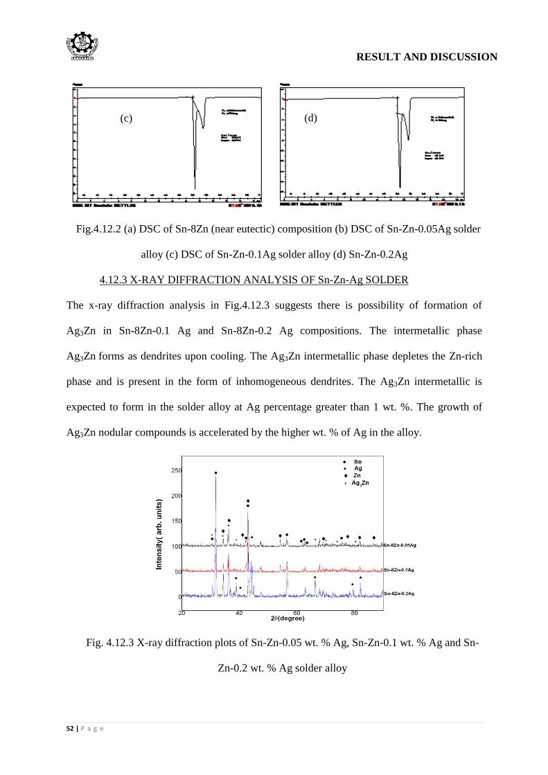
RESULT AND DISCUSSION
52 | P a g e
Fig.4.12.2 (a) DSC of Sn-8Zn (near eutectic) composition (b) DSC of Sn-Zn-0.05Ag solder
alloy (c) DSC of Sn-Zn-0.1Ag solder alloy (d) Sn-Zn-0.2Ag
4.12.3 X-RAY DIFFRACTION ANALYSIS OF Sn-Zn-Ag SOLDER
The x-ray diffraction analysis in Fig.4.12.3 suggests there is possibility of formation of
Ag3Zn in Sn-8Zn-0.1 Ag and Sn-8Zn-0.2 Ag compositions. The intermetallic phase
Ag3Zn forms as dendrites upon cooling. The Ag3Zn intermetallic phase depletes the Zn-rich
phase and is present in the form of inhomogeneous dendrites. The Ag3Zn intermetallic is
expected to form in the solder alloy at Ag percentage greater than 1 wt. %. The growth of
Ag3Zn nodular compounds is accelerated by the higher wt. % of Ag in the alloy.
Fig. 4.12.3 X-ray diffraction plots of Sn-Zn-0.05 wt. % Ag, Sn-Zn-0.1 wt. % Ag and Sn-
Zn-0.2 wt. % Ag solder alloy
(c) (d)
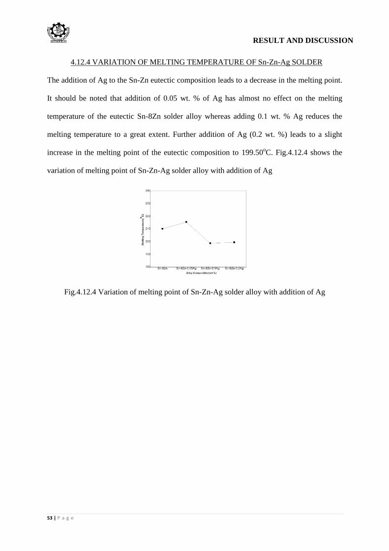
RESULT AND DISCUSSION
53 | P a g e
4.12.4 VARIATION OF MELTING TEMPERATURE OF Sn-Zn-Ag SOLDER
The addition of Ag to the Sn-Zn eutectic composition leads to a decrease in the melting point.
It should be noted that addition of 0.05 wt. % of Ag has almost no effect on the melting
temperature of the eutectic Sn-8Zn solder alloy whereas adding 0.1 wt. % Ag reduces the
melting temperature to a great extent. Further addition of Ag (0.2 wt. %) leads to a slight
increase in the melting point of the eutectic composition to 199.50oC. Fig.4.12.4 shows the
variation of melting point of Sn-Zn-Ag solder alloy with addition of Ag
Fig.4.12.4 Variation of melting point of Sn-Zn-Ag solder alloy with addition of Ag
CONCLUSION

CONCLUSIONS
54 | P a g e
1. There is significant lowering of melting temperature due to addition of Bi (upto 6 wt. %)
to the Sn-8Zn near eutectic composition. Addition of higher wt. % of Bi leads to
increase in the melting point.
2. Sn-Zn-Bi alloys do not form any intermetallic compounds between themselves. No new
compound formation was seen in the alloys.
3. Bi showed no solid solubility in Zn. Bi was seen in Sn rich regions only when the wt. %
of Bi was higher than 3 wt. %.
4. Very high wt. % of Bi in the alloy led to lower wettability of the Sn-Zn-Bi alloy on Cu
Substrate.
5. Addition of Bi leads to the decrease in percentage strain at break of the Sn-8Zn alloy. The
tensile strength of the Sn-8Zn alloy was also found to reduce with addition of Bi.
6. Addition of up to 0.1 wt. %Ag to Sn-Zn eutectic composition leads to a reduction in
melting point but further addition of Ag (0.2 wt.%) leads to slight reduction in meting
point.
7. A shoulder was observed at around 220oC in the DSC curves of Sn-Zn-0.1 wt. % Ag and
Sn-Zn-0.2 wt.% Ag alloys. This shoulder is not present 0.05 wt. % Ag containing solders.
The addition of a large amount of Ag in the Sn-Zn-0.1Ag and Sn-Zn-0.2Ag alloys
resulted in the formation of large amount of Ag3Zn intermetallic compound. This reaction
reduced the Zn content of the eutectic Sn-Zn composition which resulted in the formation
of a hypoeutectic β-Sn structure. This is why the DSC plots of the solder alloys Sn-Zn-
0.1Ag and Sn-Zn-0.2Ag showed two endothermic peaks.

SCOPE AND FUTURE WORK
55 | P a g e
1. It was observed that when Ag was added beyond 0.1% there is a possible rise in the
melting point of eutectic composition and this can be verified by adding higher wt.% of Ag to
the eutectic composition.
2. Electrical resistance of the alloys should be measured to find out their electrical resistivity.
3. Mechanical properties like elongation to failure, hardness, fractographs have to be
analyzed in order to ascertain that these alloys are not very brittle. Brittle solder alloy will
very easily break at the contact due to the formation of intermetallic
4. Elements like Al (Aluminum) can be added to the alloy to prevent oxidation of the alloys
for achieving a good solder.
REFERENCES
REFERENCES
56 | P a g e
1. Hongtao Ma, Jeffrey C. Suhling, “A review of mechanical properties of lead-free solders
for electronic packaging”, Journal of Materials Science, Volume 44(5) (2009), pp 1141-
1158.
2. C.M.L. Wua, D.Q. Yua, C.M.T. Lawa, L. Wang, “Properties of lead-free solder alloys
with rare earth element additions” Materials Science and Engineering, Volume 44(1)(
2004), pp 1–44
3. K.N. Tu, K. Zeng, “Tin–lead (Sn–Pb) solder reaction in flip chip technology”, Mater. Sci.
Eng. R, 34 (1) (2001), pp. 1–58
4. Nathan Barry, “Lead-free Solders for High-Reliability Applications: High-Cycle Fatigue
Studies” Thesis Presented to the University of Birmingham for the degree of Doctor of
Engineering (2008).
5. Directive 2002/95/EC of the European Parliament and of the Council of January 2003 on
the restriction of the use of certain hazardous substances in electrical and electronic
equipment. 2003. p. 19-23.
6. Directive 2002/96/EC of the European Parliament and of the Council of 27 January 2003
on waste electrical and electronic equipment (WEEE). 2003. p. 24-28.
7. E.P. Wood, K.L. Nimmo, “In search of new lead-free electronic solders”, J. Electron.
Mater., 23 (8) (1994), pp. 709–713
8. P. Biocca, “Global update on lead-free solders”, Surf. Mount Technol., 13 (6) (1999), pp.
64–67
9. Prerna Mishra, S.N. Alam, Rajnish Kumar, “Effect of Rare Earth elements on lead free
solder alloys” Int. Journal of Engineering Research and Applications, special issue
(2014) pp.80-86
10. Young-Sun Kima, Keun-Soo Kim, Chi-Won Hwang, Katsuaki Suganuma , “Effect of
composition and cooling rate on microstructure and tensile properties of Sn–Zn–Bi
alloys”, Journal of Alloys and Compounds Volume 352(1–2, 24)(2003), Pages 237–245
11. NCMS Lead-free Solder Project Final Report, NCMS Report 0401 RE 96National Centre
for Manufacturing Sciences, Michigan (1997)
12. A.A. El-Dalya, Y. Swilem, M.H. Makled, M.G. El-Shaarawy, A.M. Abdraboh, “Thermal
and mechanical properties of Sn–Zn–Bi lead-free solder alloys” Journal of Alloys and
Compounds Volume 484(1–2)(2009), Pages 134–142
13. J.M. Song, Z.M. Wu Scripta Mater., 54 (2006), pp. 1479–1483
14. S.C. Cheng, K.L. Lin Mater. Trans., 46 (2005), pp. 42–47
REFERENCES
57 | P a g e
15. Mishra Manas, “ A Study of Intermetallic in Cu-Sn system and Development of Sn-Zn
Based Lead Free Solders” Thesis Presented to the National Institute of Technology,
Rourkela, in partial fulfilments of the requirements for the Degree of Master of
Technology (2013).
16. Y. Chonan, T. Komiyama, J. Onuki, R. Urao, T. Kimura, T. Nagano, Mater. Trans. 43 (8)
(2002) 1887–1890.
17. S.P. Yu, H.J. Lin, M.H. Hon, M.C. Wang, J. Mater. Sci.-Mater. Electron.11 (6) (2000)
461–471.
18. NCMS Lead-free Solder Project Final Report, NCMS Report 0401 RE 96National Centre
for Manufacturing Sciences, Michigan (1997)
19. Q. Yu, H.P. Xie, L. Wang, J. Alloy Compd. 385 (1–2) (2004) 119–125.
20. K. Suganuma, K Niihara, T. Shoutoku, Y. Nakamura, J. Mater. Res.13 (10) (1998) 2859–
2865.
21. K.S. Kim, J.M. Yang, C.H. Yu, I.O. Jung, H.H. Kim, J. Alloy.Compd. 379 (2004) 314–
318.
22. I.E. Anderson, J.C. Foley, B.A. Cook, J. Harringa, R.L. Terpstra, O. Unal, “Alloying
effects in near-eutectic Sn–Ag–Cu solder alloys for improved microstructural stability”, J.
Electron. Mater., 30 (9) (2001), pp. 1050–1059
23. M. McCormack, S. Jin, G.W. Kammlott, H.S. Chen, “New Pb-free solder alloy with
superior mechanical properties” Appl. Phys. Lett., 63 (1) (1993), pp. 15–17
24. A.Z. Miric, A. Grusd, “Lead-free alloys Soldering” Surf. Mount Technol., 10 (1) (1998),
pp.19–
25. Jian Zhou , Yangshan Sun, Feng Xue., “Properties of low melting point Sn–Zn–Bi
solders” Journal of Alloys and Compounds 397 (2005) 260–264.
26. Shohji, C. Gagg, W.J. Plumbridge, J. Electron. Mater. 33 (2004) 923–927.
27. Md. Jahir Rizvi, “Experimental and Modelling Studies of Electronic Packaging
Interconnections formed with Lead-free” ,Thesis Presented to the Materials School of
Computing and Mathematical Sciences University of Greenwich London, UK for the
degree of Doctor of Engineering (2007).
28. J.h. lau , “low cost flip chip technologies for DCA, WLCSP and PGBA assemblies”,
McGraw-Hill, New York, pp.2.
29. http://www.prc.gatech.edu/academics/elpkg/pdf/module1.pdf#search=’electronic%20pac
kaging
REFERENCES
58 | P a g e
30. ASM, Welding, Brazing and Soldering. 10 ed. Metals Handbook. Vol. 6. (1990),
Washington DC: ASM International Press.
31. C.A. Harper, “Electronic Packaging & Interconnecting Handbook”, McGraw-Hill, New
York, 2nd
edition, (1997), pp.xi.
32. ANSI/IPC-T-50E Standard, “Terms and definitions for interconnecting and packaging
electronics circuits”, institute for interconnecting and packaging electronics circuit
(1992).
33. R.J.K. Wassink, “soldering in electronics”, electrochemical publications ltd., 2nd
ed.,
(1989).
34. C.A. Harper, “Electronic materials and processes Handbook”, McGraw-Hill, New York,
3rd
edition, (2003).
35. Frear, D.R., W.B. Jones, and K.R. Kinsman, “Solder Mechanics - A State of the Art
Assessment.”, Pennsylvania: The Minerals, Metals & Materials Society, (1990).
36. T.P. Vianco, Development of alternatives to lead-bearing solders, Proceedings of the
Technical Program on Surface Mount International, (19 August-2 September 1993), San
Jose, CA.
37. R.E. Reed-Hill, Physical Metallurgy Principles, PWS Publishing Company,
Massachusetts, (1994), pp. 306-307.
38. Carapella, L.A. and R. Hultgren, “The ferromagnetic nature of the beta phase in the
copper-manganese-tin system.” Transactions of the American Institute of Mining,
Metallurgical and Petroleum Engineers, 147(1942) pp. 232-242.
39. W.R. Lewis, “Notes on Soldering”, Tin Research Institute, (1961), p. 66.
40. ASM International, Electronic Material Handbook, Vol. 1, Materials Park, OH, (1989),
pp. 1161-1162.
41. Hedges, E.S., “Tin and its alloys”, London: Edward Arnold Publishers Ltd (1960).
42. Smithells, C.J., “Smithells Metals Reference Book” 7 ed, ed. E.A. Brands and G.B.
Brook. (1992), Oxford: Butterworth-Heinemann Ltd.
43. International, A., “Properties and Selection: Nonferrous Alloys and Special-Purpose
Materials” 10 ed. Metals Handbook. Vol. 2.(1990), Washington DC: ASM International
Press.
44. Harrison, M.R., J.H. Vincent, and S. H.A.H., “Lead-free reflow soldering for electronics
assembly”. Soldering & Surface Mount Technology, (2001). 13(3): pp. 21-38.
REFERENCES
59 | P a g e
45. Woolf, AD; Goldman, R; Bellinger, DC "Update on the clinical management of
childhood lead poisoning". Paediatric clinics of North America (2007).
46. Maas, RP; Patch, SC; Morgan, DM; Pandolfo, TJ, “Reducing lead exposure from
drinking water: recent history and current status". Public health reports (Washington,
D.C. 1974) (2005).
47. Mañay, N; Cousillas, AZ; Alvarez, C; Heller, T "Lead contamination in Uruguay: the
LaTeja neighborhood case". Review of environmental contamination and toxicology
(2008).
48. Staudinger KC, Roth VS, "Occupational lead poisoning"(1998).
49. Low Level Lead Exposure Harms Children: A Renewed Call for Primary Prevention".
Centres for Disease Control and Prevention. (2012).
50. Cleveland, LM; Minter, ML; Cobb, KA; Scott, AA; German, VF , "Lead hazards for
pregnant women and children”(2008).
51. Guidotti, TL; Ragain, L, "Protecting children from toxic exposure: three
strategies"(2007).
52. Rossi, E, "Low Level Environmental Lead Exposure – A Continuing Challenge".
Reviews / Australian Association of Clinical Biochemists (2008).
53. Barbosa Jr, F; Tanus-Santos, JE; Gerlach, RF; Parsons, PJ, "A Critical Review of
Biomarkers Used for Monitoring Human Exposure to Lead: Advantages, Limitations, and
Future Needs” (2005).
54. http://www.hc-sc.gc.ca/iyh-vsv/environ/lead-plomb_e.html
55. http://sis.nlm.nih.gov/enviro/lead.html
56. J. Glazer, “Microstructure and mechanical properties of Pb-free solder alloys for low cost
electronic assembly: a review”, J. Electron. Mater. 23 (8) (1994) 693-700.
57. D. Napp, “Lead-free interconnect materials for the electronics industry” in: Proceedings
of the 27th International SAMPE Technical Conference, Albuquerque, NM, 9-12 October
(1995), p. 343.
58. E. Perrot, “Electronic Packaging for the 21st Century”, Advanced Packaging, July-August
(1995).
59. ASM International, Electronic Material Handbook, Vol. 1, Materials Park, OH, (1989),
pp. 965-966.
60. Forstner, U. and Wittman, G.T., “ Metal pollution in aquatic environment” , springer
verlag Berlin, Heidelberg, New York (1979)
REFERENCES
60 | P a g e
61. Kumar, G., Singh, R.P. & Sushila, “Nitrate assimilation and biomass production in
Sesamum indicum L. seedlings in a lead enriched environment.” Water, Air & Soil Pollut.
66:163-171 (1993)
62. Wallace, A., Soufi, S.m., Alexander, C.V. & Cha, J.W., “Comparison of the effect of high
levels of DTPA and EDDHA on microelement uptake in bush bean” Commun. Soil Plant
Annal. 7:111-116 (1976)
63. Degernes, LA, “Waterfowl toxicology: a review". The veterinary clinics of North
America. Exotic animal practice 11 (2) (2008) pp: 283–300.
64. Green, RE; Hunt, WG; Parish, CN; Newton, I; Pizzari, Tom, “Effectiveness of Action to
Reduce Exposure of Free-Ranging California Condors in Arizona and Utah to Lead from
Spent Ammunition” (2008).
65. "China to relocate 15,000 from lead-poisoned area". AFP. 2009-10-16. Archived from the
original on (2009-10-19). Retrieved 2009-10-20.
66. "Aid groups say lead poisoning has killed 400 children in Nigeria". Associated Press.
(2010-10-05).
67. http://www.pb-free.info/
68. Industry Aids Environment, Japan Times, (14 October 1999), p. 10.
69. http://www.smta.org/files/SMTAI04_opening_ceremony_leadfree.pdf#search=’Solder%
20Trends%20and%20Leadfree%20Soldering%20Issues
70. http://www.fu.sav.sk/rq/projects/elfnet/docs/ELFNET_STATUS_REPORT_2004.PDF#
search=’Problems%20for%20leadfree%20implementation.
71. http://www.matrixusa.us/Technical/tech%20Lead%2oFree%20Solder_Chris%20Carabell
o.pdf’
72. J. Bath,C. Handwerker and E. Bradeley, “Research update: Lead-free solder alternatives”,
Circuits Assembly, (2000),pp. 31-40.
73. K. Suganuma, “Advances in lead-free electronics soldering”, Curr. Opin. Solid Mater.
Sci. 5 (2001) 55–64.
74. Ramani Mayappan , Ahmad Badri Ismail , Zainal Arifin Ahmad,Tadashi Ariga, Luay
Bakir Hussain, “Effect of sample perimeter and temperature on Sn–Zn based lead-free
solders”.
75. R.A. Islam, B.Y. Wu, M.O. Alam, Y.C. Chan, W. Jillek, “Investigations on micro
hardness of Sn–Zn based lead-free solder alloys as replacement of Sn–Pb solder” ,
Journal of Alloys and Compounds 392 (2005) 149–158.
REFERENCES
61 | P a g e
76. Satyanarayan, K.N. Prabhu, “Reactive wetting, evolution of interfacial and bulk IMCs
and their effect on mechanical properties of eutectic Sn–Cu solder alloy”, Advances in
Colloid and Interface Science 166 (2011) 87–118.
77. Suganuma K, Nakamura Y. “Microstructure and strength of interface between Sn–Ag
eutectic solder and Cu”, J Jpn Inst Metals 59(1995) pp :1299–305.
78. Massalski TB, Okamoto H, Subramanian PR, Kacprzak L, editors, “Binary alloy phase
diagrams”, 2nd ed, ASM International, (1990).
79. Vianco PT, Rejent JA., “Properties of ternary Sn–Ag–Bi solder alloys Part II. Wettability
and mechanical properties analyses”, J Electron Mater 28(1999) pp: 1138–43.
80. Artaki I, Jackson AM, Vianco PT., “Evaluation of lead-free solder joints in electronic
assemblies”, J Electron Mater 23(1994) pp: 757–63.
81. K.zeng, K.N Tu, “six cases of reliability study of Pb free solder joint in electronic
packaging technology”, materials science and engg, 38 (2002)
82. M.N. Croker, R.S. Fidler, R.W. “Smith The characterization of eutectic structure”, Proc.
R. Soc., London, Ser. A. 335 (1973) 15-17.
83. F.G. Yost, F.M. Hosking and D.R. Frear, “The mechanics of solder alloy wetting and
spreading”, Van Nostrand Reinhold, New York, (1993).
84. H.H. Manko, “Solder and Soldering”, 2nd Edition, McGraw-Hill, New York, (1979).
85. R.J.K. Wassink, “Soldering in Electronics, 2nd Edition, Electrochemical Publications
Ltd.”, (1989), GB-Port Erin, British Isles, pp. 36-37.
86. R.W. Wild, “Properties of Some Low Melting Fusible Alloys”, Technical Report, IBM
Federal Systems Division Laboratory, New York, (1971).
87. Akio Hirose, Hiroto Yanagawa, Eiichi Ide, Kojiro F Kobayashi, “Joint strength and
interfacial microstructure between Sn–Ag–Cu and Sn–Zn–Bi solders and Cu substrate”,
Science and Technology of Advanced Materials, Volume 5(1–2) (2004) 267–276.
88. C. Chih-ming, Yu-min Hung, L. Ching-hsuan, Journal of Alloys and Compounds,
Volume 475(1–2) (2009) 238-244.
89. Jenn-Ming Song Zong-Mou Wu Scripta Materialia Volume 54, Issue 8, (2006) 1479–
1483
90. Jiri Vizdal, Maria Helena Braga, Ales Kroupa, Klaus W. Richter, Delfim Soares,Lu´ıs
Filipe Malheiros, Jorge Ferreira, “Thermodynamic assessment of the Bi–Sn–Zn System”,
Computer Coupling of Phase Diagrams and Thermochemistry 31 (2007) 438– 448.
REFERENCES
62 | P a g e
91. Yangshan Sun, Feng Xue, Jian Zhou, “Lead-free solders based on the Sn8Zn3Bi ternary
alloy with additions of In, Nd or La”, Electronic Packaging Technology, International
Conference on - ICEPT, (2005)
92. Jian Zhou, Peipei Li, Yingying Xiao, Xiaoqing Fu, “Microstructure and Deformability of
Sn-Zn-Bi Alloys” 7th International Conference on Electronics Packaging Technology
IEEE. (2006).
93. Song, J. M. and Lin, K. L., “Behavior of intermetallics in liquid Sn–Zn–Ag solder alloys”
Journal of Materials Research, 18(9) (2003):2060-2067.
94. Chen,K. I. and Lin K. L., “The microstructures and mechanical properties of the Sn-
Zn-Ag-Al-Ga solder alloys—the effect of Ag,” Journal of Electronic Materials, 31(8)
(2002) 861-867.
95. Ahmed M., Fouzder, T., Sharif, A, Gain, A. K., Chan, Y.C., “Influence of Ag micro-
particle additions on the microstructure, hardness and tensile properties of Sn–9Zn binary
eutectic solder alloy” Microelectronics Reliability ,50: (2010) 1134–1141.