Embed Size (px)
Citation preview
Siti Rabiatull Aisha Idris et al., Int. J. Comp. Meth. and Exp. Meas., Vol. 3, No. 4 (2015) 329–339
© 2015 WIT Press, www.witpress.comISSN: 2046-0546 (paper format), ISSN: 2046-0554 (online), http://www.witpress.com/journalsDOI: 10.2495/CMEM-V3-N4-329-339
DEVELOPMENT OF DIFFUSION BARRIER LAYER ON COPPER-PRINTED CIRCUIT BOARD USING
ELECTROLESS PLATING METHOD
SITI RABIATULL AISHA IDRIS1, ALI OURDJINI2, AZMAH HANIM MOHAMAD ARIFF3 & SALIZA AZLINA OSMAN4
1Faculty of Mechanical Engineering, Universiti Malaysia Pahang, Malaysia.2Faculty of Mechanical Engineering, Universiti Teknologi Malaysia, Malaysia.
3Department of Mechanical and Manufacturing, Univerisiti Putra Malaysia, Malaysia.4Faculty of Mechanical and Manufacturing, Universiti Tun Hussein Onn Malaysia, Malaysia.
ABSTRACTIn this paper, the nickel–phosphorus (Ni–P) diffusion barrier layer between Sn–4Ag–0.5Cu solder alloy and copper-printed circuit board was developed. The electroless plating technique was used to develop Ni–P diffusion barrier layer with different percentage of phosphorus content, which are 1–5 wt% (low), 5–8 wt% (medium) and above 8 wt% (high). The results reveal that the high phosphorus content in nickel layer acts as a good diffusion barrier for Sn–4Ag–0.5Cu since it can suppress the intermetallic compound formation. This is because in higher phosphorus content, the grain boundaries were found to be eliminated. Hence, resulted in thinner intermetallic compound thickness. Keywords: diffusion barrier layer; intermetallic compound; nickel–phosphorus.
1 INTRODUCTIONPrinted circuit boards are generally fabricated in a surface-finished condition by board manufacturers and then shipped to an assembly house. There are some parts of the board, which are made of copper, left exposed for subsequent soldering. Hence, it needs protection by applying surface finish to avoid further oxidation and at the same time to maintain its solderability capability [1]. Among all metals, nickel (Ni) layer is one of the most suitable surface finish to be used as a diffusion barrier layer between copper (Cu) and tin (Sn) due to its slower diffusion rate in Sn as compared to Cu [2–4]. This situation results in producing thinner intermetallic compound (IMC) layer.
As reported in [5], nickel has been recognized as a diffusion barrier in the top surface morphology (TSM) system due to its relatively low diffusion rate through Au and Cu. Of all the Ni-plating processes, the most cost-effective option is electroless nickel–phosphorus (Ni–P). However, the phosphorus content in the electroless Ni greatly influences the interfa-cial reactions with solders. During reflow soldering, a new P-rich Ni layer is formed between the interfacial IMC and original electroless Ni–P layer [6, 7]. The formation of this P-rich compound is a new issue to be considered for the solder joint reliability.
In other works mentioned by previous researchers in [8–10], the crystallized Ni3P phase has a polycrystalline columnar structure that appears to contain defects. During reflow soldering, Kirkendall voids would form as a by-product of P-rich layer formation and these voids are claimed to be detrimental on joint reliability by resulting in brittle fracture. Besides, previous work also shows that the nature of deposit such as P content and thickness of electroless Ni–P layer might affect the fracture mode of solder joint by performing shear test [11,12].
Other than that, Kim et al. [13] and Yoon et al. [14] who used Sn–3.5Ag solder alloy mentioned that the thickness of IMC was affected by the P content, whereby lower P content
330 Siti Rabiatull Aisha Idris et al., Int. J. Comp. Meth. and Exp. Meas., Vol. 3, No. 4 (2015)
(7 wt%) produced thicker IMC than higher P content (10 wt%). Laurila and Vuorinen [15] also found that Ni3P IMC formation can be suppressed when the P content reached 30 at%. However, the researchers did not mention the exact reason of what was happening to the surface of the coated copper when different P content was used.
From the above-mentioned studies, it can be concluded that the fundamental understand-ing in the area of solder metallurgy in solder interconnect was still lacking. This is especially important after the industry switch to lead-free solders was implemented in July 2006. There-fore, an experimental investigation was conducted to explore the effect of Ni–P layer, which contained 1–5 wt% (low P), 5–8 wt% (medium P) and above 8 wt% (high P) of the copper circuitry on printed circuit boards when using Sn–3Ag–0.Cu solder alloy. Besides, the micro-structural characteristics of the coating and the thickness of the IMC layer were also analysed and measured to evaluate the Ni–P layer diffusion rate.
2 MATERIALS AND METHODMaterials preparation is divided into two steps, which is explained in the following section:
2.1 Surface finish deposition
The as-received fibre-glass epoxy material (FR-4) with the thickness of 1 mm was cut into 50 mm × 80 mm and used as the substrate material. The substrates were mechanically ground using silicon carbide paper of 1000 grit and 4000 grit since it can give suitable surface rough-ness, which was 0.073 Ra. The substrate materials then had gone through a precleaning step to produce an oxide-free surface and also activate its surface at the same time. After that, the substrates were plated in nickel solution. Three types of electroless nickel were used in this research to produce coatings with three different phosphorus contents. Solution for high P and low P is prepared in laboratory while the nickel containing medium P was a commercial one. The combination for laboratory prepared Ni solutions is shown in Table 1. Thiourea was added as the stabilizer to prevent decomposition of the solutions for low and high P baths. The quantity of thiourea is very important as too much of it would slow down the plating process.
The medium P solution is called NIMUDEN 5X, a high-temperature acidic solution (90–92°C, pH 4.3–4.5). It is usually used in the industry to produce coating with phosphorus content between 5 wt% and 10 wt%. To make-up the solution, four parts of the distilled water are mixed into one part of NIMUDEN 5X. The solution is then placed into the plating bath. Sodium hydroxide and sulphuric acid are used to control the pH value to the required range. If the pH value runs below 4.0, plating speed decreases and if the value runs above 4.6, plat-ing solution sometimes become muddy. For this solution, plating time of 50 min produced ~6.070 μm of Ni thickness.
2.2 Solder bump formation and materials characterization
First, the substrates were coated with a thin layer of no clean flux to improve wetting of molten solder during soldering. Then, the substrates were manually populated with lead-free Sn–3Ag–0.5Cu solder balls with 500 μm in diameter arranged in several rows on top of cop-per substrate. Bonding to form the solder joints was made by reflow in a resistance furnace with the peak reflow temperature set at 250°C for lead-free Sn–Ag–Cu solder for about 6 min. The samples were then subjected to isothermal aging at 150°C for up to 2000 h.

Siti Rabiatull Aisha Idris et al., Int. J. Comp. Meth. and Exp. Meas., Vol. 3, No. 4 (2015) 331
Cross-sections from the samples were prepared and examined by means of optical and electron scanning microscopy. Energy dispersive X-ray (EDX) and X-ray diffraction (XRD) were used to identify the chemical elements in the microstructure. The average thickness of the IMC formed is measured using EDX spot analysis across the intermetallic layer on cross-sections of the solder joints.
3 RESULTS AND DISCUSSION
3.1 Diffusion barrier layer
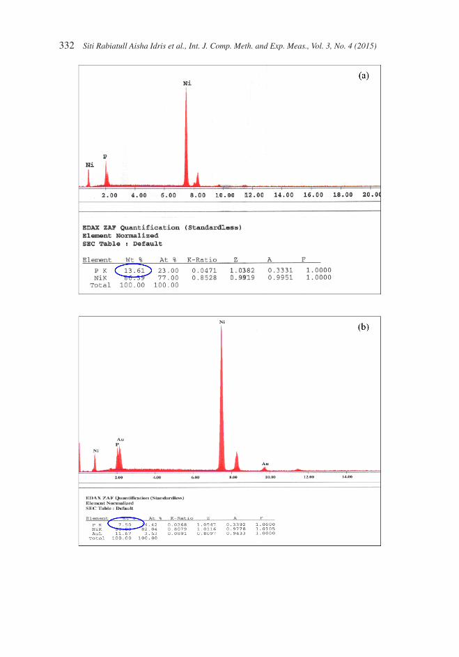
Electroless nickel with phosphorus as reducing agent has been selected as the barrier layer for this research. According to Yli-Pentti [5], electroless Ni–P has been considered as a promis-ing finish due to its many advantages such as excellent selective deposition, good corrosion resistivity, strong adhesion, easy processing and low cost. Furthermore, the IMC growth has been found to be minimized in the case of Ni finish, as the reaction between Ni and Sn is much slower than between Cu and Sn. Electroless nickel coatings are not pure nickel depos-its but rather alloys of nickel and other compounds such as phosphorus or boron, depending on the reducing agent used during deposition. Because of the low solubility of these com-pounds in a nickel matrix, the coatings obtained are supersaturated solutions of either phosphorus or boron in nickel. This low solubility drastically alters the microstructure of the metal coating. In general, the electroless nickel–phosphorus (Ni–P) deposits can be classified as low (1–5 wt% P), medium (5–8 wt% P) and high (9 wt% P and more) phosphorus deposits based on their phosphorus contents. Results showed that the as-deposited, low concentrations of phosphorus in nickel result in a microcrystalline or crystalline coating, whereas medium level of phosphorus yields coatings that contain both crystalline and amorphous nickel phases. High concentrations of phosphorus produce electroless nickel deposits that are com-pletely amorphous, mixtures of amorphous and microcrystalline nickel or those mixtures plus various other intermediate phases like Ni, Ni3P, Ni12P5 and Ni2P.
Figure 1 shows the EDX results of the as-deposited nickel layer containing different phos-phorus contents: low phosphorus, medium phosphorus and high phosphorus. During electroless nickel plating, the atomic ratio of consumed Ni2
+ and H2PO2 is about 1:3.3, so the consumption of H2PO2 is much faster than that of Ni2
+. After a period of deposition, the
Table 1: Chemical components for electroless Ni–P plating.
Chemicals/parametersQuantity
Low p High P
Nickel sulphate (g/L) 33 28
Sodium citrate (g/L) 84 –
Sodium acetate (g/L) – 17
Ammonium chloride (g/L) – 50
Sodium hypophosphite (g/L) 17 24
pH 9.5 4.4
Temperature (°C) 85 88
332 Siti Rabiatull Aisha Idris et al., Int. J. Comp. Meth. and Exp. Meas., Vol. 3, No. 4 (2015)
Siti Rabiatull Aisha Idris et al., Int. J. Comp. Meth. and Exp. Meas., Vol. 3, No. 4 (2015) 333
concentration of H2PO2 will be much lower than that in the fresh solution. Because the phos-phorus in the Ni–P coatings comes from the H2PO2
- in the solution and a low reactant concentration will result in a low reaction rate, the solution after several plating operations will produce Ni–P coatings with lower phosphorus content. It is quite difficult to control the phosphorus content in the Ni–P coating, so there will always be some variation during test-ing. The results were in the same argument with [2, 16, 17]. In this research, we selected to follow the general classification of Ni–P deposits; low (1–5 wt% P), medium (5–8 wt% P) and high (9 wt% P and more).
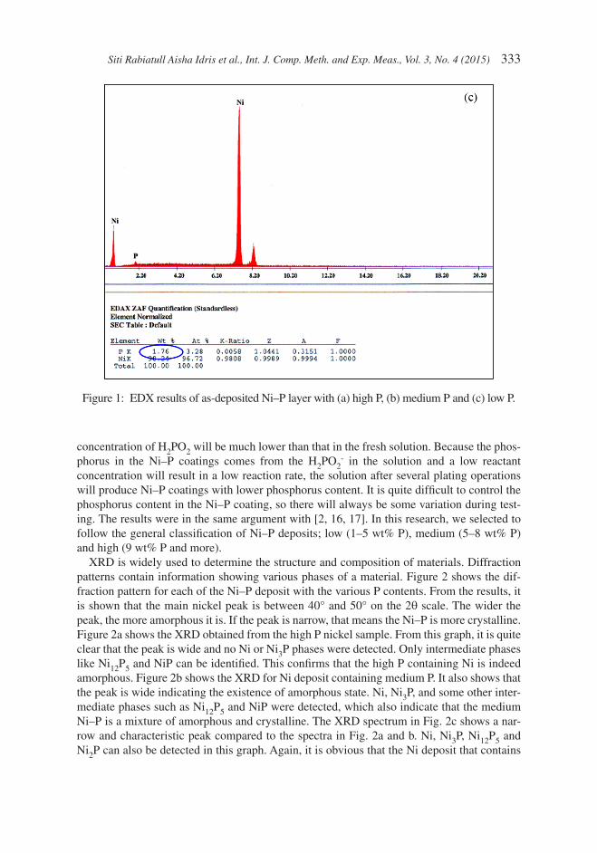
XRD is widely used to determine the structure and composition of materials. Diffraction patterns contain information showing various phases of a material. Figure 2 shows the dif-fraction pattern for each of the Ni–P deposit with the various P contents. From the results, it is shown that the main nickel peak is between 40° and 50° on the 2θ scale. The wider the peak, the more amorphous it is. If the peak is narrow, that means the Ni–P is more crystalline. Figure 2a shows the XRD obtained from the high P nickel sample. From this graph, it is quite clear that the peak is wide and no Ni or Ni3P phases were detected. Only intermediate phases like Ni12P5 and NiP can be identified. This confirms that the high P containing Ni is indeed amorphous. Figure 2b shows the XRD for Ni deposit containing medium P. It also shows that the peak is wide indicating the existence of amorphous state. Ni, Ni3P, and some other inter-mediate phases such as Ni12P5 and NiP were detected, which also indicate that the medium Ni–P is a mixture of amorphous and crystalline. The XRD spectrum in Fig. 2c shows a nar-row and characteristic peak compared to the spectra in Fig. 2a and b. Ni, Ni3P, Ni12P5 and Ni2P can also be detected in this graph. Again, it is obvious that the Ni deposit that contains
Figure 1: EDX results of as-deposited Ni–P layer with (a) high P, (b) medium P and (c) low P.

334 Siti Rabiatull Aisha Idris et al., Int. J. Comp. Meth. and Exp. Meas., Vol. 3, No. 4 (2015)
Figure 2: XRD results of electroless Ni surface finish with different concentrations of P: (a) high P nickel, (b) medium P nickel and (c) low P nickel.
Siti Rabiatull Aisha Idris et al., Int. J. Comp. Meth. and Exp. Meas., Vol. 3, No. 4 (2015) 335
low P content is a mixture of amorphous and crystalline phases, but compared to medium P, low Ni–P sample is more crystalline.
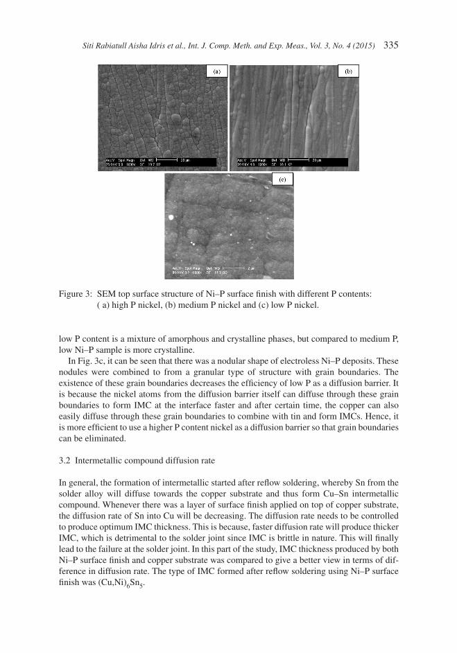
In Fig. 3c, it can be seen that there was a nodular shape of electroless Ni–P deposits. These nodules were combined to from a granular type of structure with grain boundaries. The existence of these grain boundaries decreases the efficiency of low P as a diffusion barrier. It is because the nickel atoms from the diffusion barrier itself can diffuse through these grain boundaries to form IMC at the interface faster and after certain time, the copper can also easily diffuse through these grain boundaries to combine with tin and form IMCs. Hence, it is more efficient to use a higher P content nickel as a diffusion barrier so that grain boundaries can be eliminated.
3.2 Intermetallic compound diffusion rate
In general, the formation of intermetallic started after reflow soldering, whereby Sn from the solder alloy will diffuse towards the copper substrate and thus form Cu–Sn intermetallic compound. Whenever there was a layer of surface finish applied on top of copper substrate, the diffusion rate of Sn into Cu will be decreasing. The diffusion rate needs to be controlled to produce optimum IMC thickness. This is because, faster diffusion rate will produce thicker IMC, which is detrimental to the solder joint since IMC is brittle in nature. This will finally lead to the failure at the solder joint. In this part of the study, IMC thickness produced by both Ni–P surface finish and copper substrate was compared to give a better view in terms of dif-ference in diffusion rate. The type of IMC formed after reflow soldering using Ni–P surface finish was (Cu,Ni)6Sn5.
Figure 3: SEM top surface structure of Ni–P surface finish with different P contents: ( a) high P nickel, (b) medium P nickel and (c) low P nickel.
336 Siti Rabiatull Aisha Idris et al., Int. J. Comp. Meth. and Exp. Meas., Vol. 3, No. 4 (2015)
Generally, the thickness of a reaction layer in the diffusion couples can be expressed by the simple parabolic equation
W=ktn (1)
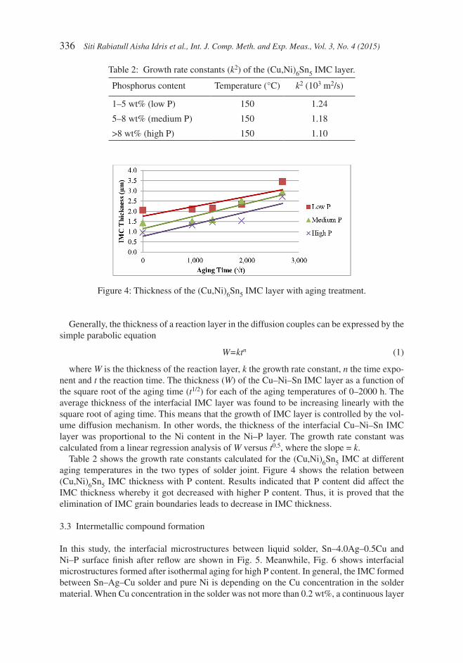
where W is the thickness of the reaction layer, k the growth rate constant, n the time expo-nent and t the reaction time. The thickness (W) of the Cu–Ni–Sn IMC layer as a function of the square root of the aging time (t1/2) for each of the aging temperatures of 0–2000 h. The average thickness of the interfacial IMC layer was found to be increasing linearly with the square root of aging time. This means that the growth of IMC layer is controlled by the vol-ume diffusion mechanism. In other words, the thickness of the interfacial Cu–Ni–Sn IMC layer was proportional to the Ni content in the Ni–P layer. The growth rate constant was calculated from a linear regression analysis of W versus t0.5, where the slope = k.
Table 2 shows the growth rate constants calculated for the (Cu,Ni)6Sn5 IMC at different aging temperatures in the two types of solder joint. Figure 4 shows the relation between (Cu,Ni)6Sn5 IMC thickness with P content. Results indicated that P content did affect the IMC thickness whereby it got decreased with higher P content. Thus, it is proved that the elimination of IMC grain boundaries leads to decrease in IMC thickness.
3.3 Intermetallic compound formation
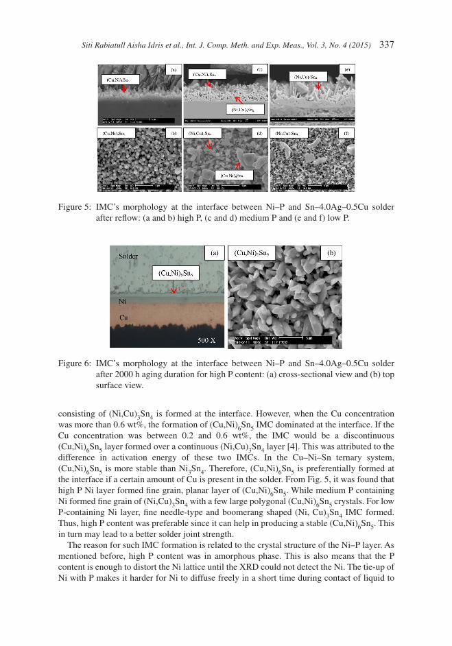
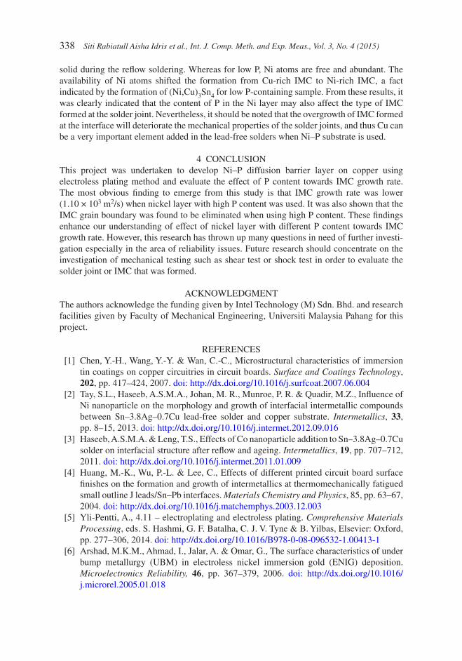
In this study, the interfacial microstructures between liquid solder, Sn–4.0Ag–0.5Cu and Ni–P surface finish after reflow are shown in Fig. 5. Meanwhile, Fig. 6 shows interfacial microstructures formed after isothermal aging for high P content. In general, the IMC formed between Sn–Ag–Cu solder and pure Ni is depending on the Cu concentration in the solder material. When Cu concentration in the solder was not more than 0.2 wt%, a continuous layer
Table 2: Growth rate constants (k2) of the (Cu,Ni)6Sn5 IMC layer.
Phosphorus content Temperature (°C) k2 (103 m2/s)
1–5 wt% (low P) 150 1.24
5–8 wt% (medium P) 150 1.18
>8 wt% (high P) 150 1.10
Figure 4: Thickness of the (Cu,Ni)6Sn5 IMC layer with aging treatment.
Siti Rabiatull Aisha Idris et al., Int. J. Comp. Meth. and Exp. Meas., Vol. 3, No. 4 (2015) 337
Figure 5: IMC’s morphology at the interface between Ni–P and Sn–4.0Ag–0.5Cu solder after reflow: (a and b) high P, (c and d) medium P and (e and f) low P.
Figure 6: IMC’s morphology at the interface between Ni–P and Sn–4.0Ag–0.5Cu solder after 2000 h aging duration for high P content: (a) cross-sectional view and (b) top surface view.
consisting of (Ni,Cu)3Sn4 is formed at the interface. However, when the Cu concentration was more than 0.6 wt%, the formation of (Cu,Ni)6Sn5 IMC dominated at the interface. If the Cu concentration was between 0.2 and 0.6 wt%, the IMC would be a discontinuous (Cu,Ni)6Sn5 layer formed over a continuous (Ni,Cu)3Sn4 layer [4]. This was attributed to the difference in activation energy of these two IMCs. In the Cu–Ni–Sn ternary system, (Cu,Ni)6Sn5 is more stable than Ni3Sn4. Therefore, (Cu,Ni)6Sn5 is preferentially formed at the interface if a certain amount of Cu is present in the solder. From Fig. 5, it was found that high P Ni layer formed fine grain, planar layer of (Cu,Ni)6Sn5. While medium P containing Ni formed fine grain of (Ni,Cu)3Sn4 with a few large polygonal (Cu,Ni)6Sn5 crystals. For low P-containing Ni layer, fine needle-type and boomerang shaped (Ni, Cu)3Sn4 IMC formed. Thus, high P content was preferable since it can help in producing a stable (Cu,Ni)6Sn5. This in turn may lead to a better solder joint strength.
The reason for such IMC formation is related to the crystal structure of the Ni–P layer. As mentioned before, high P content was in amorphous phase. This is also means that the P content is enough to distort the Ni lattice until the XRD could not detect the Ni. The tie-up of Ni with P makes it harder for Ni to diffuse freely in a short time during contact of liquid to
338 Siti Rabiatull Aisha Idris et al., Int. J. Comp. Meth. and Exp. Meas., Vol. 3, No. 4 (2015)
solid during the reflow soldering. Whereas for low P, Ni atoms are free and abundant. The availability of Ni atoms shifted the formation from Cu-rich IMC to Ni-rich IMC, a fact indicated by the formation of (Ni,Cu)3Sn4 for low P-containing sample. From these results, it was clearly indicated that the content of P in the Ni layer may also affect the type of IMC formed at the solder joint. Nevertheless, it should be noted that the overgrowth of IMC formed at the interface will deteriorate the mechanical properties of the solder joints, and thus Cu can be a very important element added in the lead-free solders when Ni–P substrate is used.
4 CONCLUSIONThis project was undertaken to develop Ni–P diffusion barrier layer on copper using electroless plating method and evaluate the effect of P content towards IMC growth rate. The most obvious finding to emerge from this study is that IMC growth rate was lower (1.10 × 10³ m2/s) when nickel layer with high P content was used. It was also shown that the IMC grain boundary was found to be eliminated when using high P content. These findings enhance our understanding of effect of nickel layer with different P content towards IMC growth rate. However, this research has thrown up many questions in need of further investi-gation especially in the area of reliability issues. Future research should concentrate on the investigation of mechanical testing such as shear test or shock test in order to evaluate the solder joint or IMC that was formed.
ACKNOWLEDGMENTThe authors acknowledge the funding given by Intel Technology (M) Sdn. Bhd. and research facilities given by Faculty of Mechanical Engineering, Universiti Malaysia Pahang for this project.
REFERENCES [1] Chen, Y.-H., Wang, Y.-Y. & Wan, C.-C., Microstructural characteristics of immersion
tin coatings on copper circuitries in circuit boards. Surface and Coatings Technology, 202, pp. 417–424, 2007. doi: http://dx.doi.org/10.1016/j.surfcoat.2007.06.004
[2] Tay, S.L., Haseeb, A.S.M.A., Johan, M. R., Munroe, P. R. & Quadir, M.Z., Influence of Ni nanoparticle on the morphology and growth of interfacial intermetallic compounds between Sn–3.8Ag–0.7Cu lead-free solder and copper substrate. Intermetallics, 33, pp. 8–15, 2013. doi: http://dx.doi.org/10.1016/j.intermet.2012.09.016
[3] Haseeb, A.S.M.A. & Leng, T.S., Effects of Co nanoparticle addition to Sn–3.8Ag–0.7Cu solder on interfacial structure after reflow and ageing. Intermetallics, 19, pp. 707–712, 2011. doi: http://dx.doi.org/10.1016/j.intermet.2011.01.009
[4] Huang, M.-K., Wu, P.-L. & Lee, C., Effects of different printed circuit board surface finishes on the formation and growth of intermetallics at thermomechanically fatigued small outline J leads/Sn–Pb interfaces. Materials Chemistry and Physics, 85, pp. 63–67, 2004. doi: http://dx.doi.org/10.1016/j.matchemphys.2003.12.003
[5] Yli-Pentti, A., 4.11 – electroplating and electroless plating. Comprehensive Materials Processing, eds. S. Hashmi, G. F. Batalha, C. J. V. Tyne & B. Yilbas, Elsevier: Oxford, pp. 277–306, 2014. doi: http://dx.doi.org/10.1016/B978-0-08-096532-1.00413-1
[6] Arshad, M.K.M., Ahmad, I., Jalar, A. & Omar, G., The surface characteristics of under bump metallurgy (UBM) in electroless nickel immersion gold (ENIG) deposition. Microelectronics Reliability, 46, pp. 367–379, 2006. doi: http://dx.doi.org/10.1016/ j.microrel.2005.01.018
Siti Rabiatull Aisha Idris et al., Int. J. Comp. Meth. and Exp. Meas., Vol. 3, No. 4 (2015) 339
[7] Aisha, I.S.R., Ourdjini, A., Hanim, M.A. & Azlina, O.S., Effect of reflow profile on intermetallic compound formation. IOP Conference Series: Materials Science and Engi-neering, 46, p. 012037, 2013. doi: http://dx.doi.org/10.1088/1757-899X/46/1/012037
[8] Zeng, K. & Tu, K.N., Six cases of reliability study of Pb-free solder joints in electronic packaging technology. Materials Science and Engineering: R: Reports, 38, pp. 55–105, 2002. doi: http://dx.doi.org/10.1016/S0927-796X(02)00007-4
[9] Farzaneh, A., Mohammadi, M., Ehteshamzadeh, M. & Mohammadi, F., Electro-chemical and structural properties of electroless Ni–P–SiC nanocomposite coatings. Applied Surface Science, 276, pp. 697–704, 2013. doi: http://dx.doi.org/10.1016/ j.apsusc.2013.03.156
[10] Rahmat, M.A., Oskouei, R.H., Ibrahim, R.N. & Singh Raman, R.K., The effect of elec-troless Ni–P coatings on the fatigue life of Al 7075-T6 fastener holes with symmetrical slits. International Journal of Fatigue, 52, pp. 30–38, 2013. doi: http://dx.doi.org/10.1016/j.ijfatigue.2013.02.007
[11] Ramesh, C.S., Keshavamurthy, R., Channabasappa, B.H. & Ahmed, A., Microstructure and mechanical properties of Ni–P-coated Si3N4 reinforced Al6061 composites. Materials Science and Engineering: A, 502, pp. 99–106, 2009. doi: http://dx.doi.org/ 10.1016/j.msea.2008.10.012
[12] Alam, M.O., Chan, Y.C. & Hung, K.C., Reliability study of the electroless Ni–P layer against solder alloy, Microelectronics Reliability, 42, pp. 1065–1073, 2002. doi: http://dx.doi.org/10.1016/S0026-2714(02)00068-9
[13] Kim, J.-M., Jeong, M.-H., Yoo, S., Lee, C.-W. & Park, Y.-B., Effects of surface finishes and loading speeds on shear strength of Sn–3.0Ag–0.5Cu solder joints. Microelectronic Engineering, 89, pp. 55–57, 2012. doi: http://dx.doi.org/10.1016/j.mee.2011.03.148
[14] Yoon, J.-W., Park, J.-H., Shur, C.-C. & Jung, S.-B., Characteristic evaluation of electroless nickel–phosphorus deposits with different phosphorus contents. Micro-electronic Engineering, 84, pp. 2552–2557, 2007. doi: http://dx.doi.org/10.1016/ j.mee.2007.05.057
[15] Laurila, T. & Vuorinen, V., Combined thermodynamic-kinetic analysis of the inter-facial reactions between Ni metallization and various lead-free solders. Materials, 2, pp. 1796–1834, 2009. doi: http://dx.doi.org/10.3390/ma2041796
[16] Saliza Azlina, O., Ourdjini, A. & Siti Rabiatull Aisha, I., Effect of nickel doping on interfacial reaction between lead-free solder and Ni–P substrate. Advanced Materi-als Research, 488–489, pp. 1375–1379, 2012. doi: http://dx.doi.org/10.4028/www. scientific.net/AMR.488-489.1375
[17] Chavali, S., Singh, Y., Subbarayan, G., Bansal, A. & Ahmad, M., Effect of pad surface finish and reflow cooling rate on the microstructure and the mechanical behavior of SnAgCu solder alloys. Microelectronics Reliability, 53, pp. 892–898, 2013. doi: http://dx.doi.org/10.1016/j.microrel.2013.02.006